US11832467B2 - Light-emitting device and electronic apparatus including the same - Google Patents
Light-emitting device and electronic apparatus including the same Download PDFInfo
- Publication number
- US11832467B2 US11832467B2 US17/223,952 US202117223952A US11832467B2 US 11832467 B2 US11832467 B2 US 11832467B2 US 202117223952 A US202117223952 A US 202117223952A US 11832467 B2 US11832467 B2 US 11832467B2
- Authority
- US
- United States
- Prior art keywords
- group
- dopant
- light
- electrode
- emitting device
- Prior art date
- Legal status (The legal status is an assumption and is not a legal conclusion. Google has not performed a legal analysis and makes no representation as to the accuracy of the status listed.)
- Active, expires
Links
Images


Classifications
-
- H—ELECTRICITY
- H10—SEMICONDUCTOR DEVICES; ELECTRIC SOLID-STATE DEVICES NOT OTHERWISE PROVIDED FOR
- H10K—ORGANIC ELECTRIC SOLID-STATE DEVICES
- H10K50/00—Organic light-emitting devices
- H10K50/10—OLEDs or polymer light-emitting diodes [PLED]
- H10K50/11—OLEDs or polymer light-emitting diodes [PLED] characterised by the electroluminescent [EL] layers
- H10K50/12—OLEDs or polymer light-emitting diodes [PLED] characterised by the electroluminescent [EL] layers comprising dopants
- H10K50/121—OLEDs or polymer light-emitting diodes [PLED] characterised by the electroluminescent [EL] layers comprising dopants for assisting energy transfer, e.g. sensitization
-
- H—ELECTRICITY
- H10—SEMICONDUCTOR DEVICES; ELECTRIC SOLID-STATE DEVICES NOT OTHERWISE PROVIDED FOR
- H10K—ORGANIC ELECTRIC SOLID-STATE DEVICES
- H10K50/00—Organic light-emitting devices
- H10K50/10—OLEDs or polymer light-emitting diodes [PLED]
- H10K50/11—OLEDs or polymer light-emitting diodes [PLED] characterised by the electroluminescent [EL] layers
- H10K50/12—OLEDs or polymer light-emitting diodes [PLED] characterised by the electroluminescent [EL] layers comprising dopants
-
- H—ELECTRICITY
- H10—SEMICONDUCTOR DEVICES; ELECTRIC SOLID-STATE DEVICES NOT OTHERWISE PROVIDED FOR
- H10K—ORGANIC ELECTRIC SOLID-STATE DEVICES
- H10K50/00—Organic light-emitting devices
- H10K50/10—OLEDs or polymer light-emitting diodes [PLED]
- H10K50/11—OLEDs or polymer light-emitting diodes [PLED] characterised by the electroluminescent [EL] layers
- H10K50/125—OLEDs or polymer light-emitting diodes [PLED] characterised by the electroluminescent [EL] layers specially adapted for multicolour light emission, e.g. for emitting white light
- H10K50/13—OLEDs or polymer light-emitting diodes [PLED] characterised by the electroluminescent [EL] layers specially adapted for multicolour light emission, e.g. for emitting white light comprising stacked EL layers within one EL unit
-
- H—ELECTRICITY
- H10—SEMICONDUCTOR DEVICES; ELECTRIC SOLID-STATE DEVICES NOT OTHERWISE PROVIDED FOR
- H10K—ORGANIC ELECTRIC SOLID-STATE DEVICES
- H10K59/00—Integrated devices, or assemblies of multiple devices, comprising at least one organic light-emitting element covered by group H10K50/00
- H10K59/10—OLED displays
- H10K59/12—Active-matrix OLED [AMOLED] displays
-
- H—ELECTRICITY
- H10—SEMICONDUCTOR DEVICES; ELECTRIC SOLID-STATE DEVICES NOT OTHERWISE PROVIDED FOR
- H10K—ORGANIC ELECTRIC SOLID-STATE DEVICES
- H10K59/00—Integrated devices, or assemblies of multiple devices, comprising at least one organic light-emitting element covered by group H10K50/00
- H10K59/30—Devices specially adapted for multicolour light emission
- H10K59/38—Devices specially adapted for multicolour light emission comprising colour filters or colour changing media [CCM]
-
- H—ELECTRICITY
- H10—SEMICONDUCTOR DEVICES; ELECTRIC SOLID-STATE DEVICES NOT OTHERWISE PROVIDED FOR
- H10K—ORGANIC ELECTRIC SOLID-STATE DEVICES
- H10K85/00—Organic materials used in the body or electrodes of devices covered by this subclass
- H10K85/30—Coordination compounds
- H10K85/321—Metal complexes comprising a group IIIA element, e.g. Tris (8-hydroxyquinoline) gallium [Gaq3]
- H10K85/322—Metal complexes comprising a group IIIA element, e.g. Tris (8-hydroxyquinoline) gallium [Gaq3] comprising boron
-
- H—ELECTRICITY
- H10—SEMICONDUCTOR DEVICES; ELECTRIC SOLID-STATE DEVICES NOT OTHERWISE PROVIDED FOR
- H10K—ORGANIC ELECTRIC SOLID-STATE DEVICES
- H10K85/00—Organic materials used in the body or electrodes of devices covered by this subclass
- H10K85/30—Coordination compounds
- H10K85/341—Transition metal complexes, e.g. Ru(II)polypyridine complexes
- H10K85/346—Transition metal complexes, e.g. Ru(II)polypyridine complexes comprising platinum
-
- H—ELECTRICITY
- H10—SEMICONDUCTOR DEVICES; ELECTRIC SOLID-STATE DEVICES NOT OTHERWISE PROVIDED FOR
- H10K—ORGANIC ELECTRIC SOLID-STATE DEVICES
- H10K85/00—Organic materials used in the body or electrodes of devices covered by this subclass
- H10K85/60—Organic compounds having low molecular weight
- H10K85/649—Aromatic compounds comprising a hetero atom
- H10K85/657—Polycyclic condensed heteroaromatic hydrocarbons
- H10K85/6572—Polycyclic condensed heteroaromatic hydrocarbons comprising only nitrogen in the heteroaromatic polycondensed ring system, e.g. phenanthroline or carbazole
-
- H—ELECTRICITY
- H10—SEMICONDUCTOR DEVICES; ELECTRIC SOLID-STATE DEVICES NOT OTHERWISE PROVIDED FOR
- H10K—ORGANIC ELECTRIC SOLID-STATE DEVICES
- H10K2101/00—Properties of the organic materials covered by group H10K85/00
-
- H—ELECTRICITY
- H10—SEMICONDUCTOR DEVICES; ELECTRIC SOLID-STATE DEVICES NOT OTHERWISE PROVIDED FOR
- H10K—ORGANIC ELECTRIC SOLID-STATE DEVICES
- H10K2101/00—Properties of the organic materials covered by group H10K85/00
- H10K2101/20—Delayed fluorescence emission
-
- H—ELECTRICITY
- H10—SEMICONDUCTOR DEVICES; ELECTRIC SOLID-STATE DEVICES NOT OTHERWISE PROVIDED FOR
- H10K—ORGANIC ELECTRIC SOLID-STATE DEVICES
- H10K2101/00—Properties of the organic materials covered by group H10K85/00
- H10K2101/30—Highest occupied molecular orbital [HOMO], lowest unoccupied molecular orbital [LUMO] or Fermi energy values
-
- H—ELECTRICITY
- H10—SEMICONDUCTOR DEVICES; ELECTRIC SOLID-STATE DEVICES NOT OTHERWISE PROVIDED FOR
- H10K—ORGANIC ELECTRIC SOLID-STATE DEVICES
- H10K2101/00—Properties of the organic materials covered by group H10K85/00
- H10K2101/80—Composition varying spatially, e.g. having a spatial gradient
-
- H—ELECTRICITY
- H10—SEMICONDUCTOR DEVICES; ELECTRIC SOLID-STATE DEVICES NOT OTHERWISE PROVIDED FOR
- H10K—ORGANIC ELECTRIC SOLID-STATE DEVICES
- H10K85/00—Organic materials used in the body or electrodes of devices covered by this subclass
- H10K85/30—Coordination compounds
- H10K85/341—Transition metal complexes, e.g. Ru(II)polypyridine complexes
- H10K85/342—Transition metal complexes, e.g. Ru(II)polypyridine complexes comprising iridium
-
- H—ELECTRICITY
- H10—SEMICONDUCTOR DEVICES; ELECTRIC SOLID-STATE DEVICES NOT OTHERWISE PROVIDED FOR
- H10K—ORGANIC ELECTRIC SOLID-STATE DEVICES
- H10K85/00—Organic materials used in the body or electrodes of devices covered by this subclass
- H10K85/60—Organic compounds having low molecular weight
- H10K85/649—Aromatic compounds comprising a hetero atom
- H10K85/657—Polycyclic condensed heteroaromatic hydrocarbons
-
- H—ELECTRICITY
- H10—SEMICONDUCTOR DEVICES; ELECTRIC SOLID-STATE DEVICES NOT OTHERWISE PROVIDED FOR
- H10K—ORGANIC ELECTRIC SOLID-STATE DEVICES
- H10K85/00—Organic materials used in the body or electrodes of devices covered by this subclass
- H10K85/60—Organic compounds having low molecular weight
- H10K85/658—Organoboranes
Definitions
- One or more embodiments relate to a light-emitting device and an electronic apparatus including the same.
- Light-emitting devices are self-emission devices that have wide viewing angles, high contrast ratios, short response times, and excellent characteristics in terms of brightness, driving voltage, and response speed, compared to other devices in the art.
- a first electrode is arranged on a substrate, and a hole transport region, an emission layer, an electron transport region, and a second electrode are sequentially formed on the first electrode. Holes provided from the first electrode may move toward the emission layer through the hole transport region, and electrons provided from the second electrode may move toward the emission layer through the electron transport region. Carriers, such as holes and electrons, recombine in the emission layer to produce excitons. These excitons transition from an excited state to a ground state to thereby generate light.
- One or more embodiments include a device of hyper-fluorescence system in which a light-emitting zone is maximized.
- a light-emitting composition includes
- the first emission layer includes a first dopant and a second dopant, where the second dopant is an electron-trapping dopant, and
- an electronic apparatus includes the light-emitting device.
- FIG. 1 is a schematic view of a light-emitting device according to an exemplary embodiment
- FIG. 2 is a cross-sectional view of a light-emitting apparatus according to another exemplary embodiment.
- FIG. 3 is a cross-sectional view of a light-emitting apparatus according to another exemplary embodiment.
- relative terms such as “lower” or “bottom” and “upper” or “top,” may be used herein to describe one element's relationship to another element as illustrated in the Figures It will be understood that relative terms are intended to encompass different orientations of the device in addition to the orientation depicted in the Figures
- the exemplary term “lower,” can therefore, encompasses both an orientation of “lower” and “upper,” depending on the particular orientation of the figure
- elements described as “below” or “beneath” other elements would then be oriented “above” the other elements
- the exemplary terms “below” or “beneath” can, therefore, encompass both an orientation of above and below.
- “About” or “approximately” as used herein is inclusive of the stated value and means within an acceptable range of deviation for the particular value as determined by one of ordinary skill in the art, considering the measurement in question and the error associated with measurement of the particular quantity (i.e., the limitations of the measurement system). For example, “about” can mean within one or more standard deviations, or within ⁇ 30%, 20%, 10% or 5% of the stated value.
- Exemplary embodiments are described herein with reference to cross section illustrations that are schematic illustrations of idealized embodiments As such, variations from the shapes of the illustrations as a result, for example, of manufacturing techniques and/or tolerances, are to be expected Thus, embodiments described herein should not be construed as limited to the particular shapes of regions as illustrated herein but are to include deviations in shapes that result, for example, from manufacturing. For example, a region illustrated or described as flat may, typically, have rough and/or nonlinear features Moreover, sharp angles that are illustrated may be rounded Thus, the regions illustrated in the figures are schematic in nature and their shapes are not intended to illustrate the precise shape of a region and are not intended to limit the scope of the present claims.
- An aspect of the present disclosure provides a light-emitting device including:
- the emission layer includes a first emission layer and a second emission layer
- the first emission layer includes a first dopant and a second dopant, wherein the second dopant is an electron-trapping dopant, and
- the second emission layer includes a third dopant and a fourth dopant, wherein the fourth dopant is a hole-trapping dopant.
- second dopant may be used interchangeably with the term “electron-trapping dopant.”
- fourth dopant may be used interchangeably with the term “hole-trapping dopant.”
- the first electrode may be an anode
- the second electrode may be a cathode
- the interlayer may further include a hole transport region that is arranged between the first electrode and the emission layer and includes a hole injection layer, a hole transport layer, an electron blocking layer, or a combination thereof.
- the first electrode may be an anode
- the second electrode may be a cathode
- the interlayer may further include an electron transport region that is arranged between the emission layer and the second electrode and includes a hole blocking layer, an electron transport layer, an electron injection layer, or a combination thereof.
- the first emission layer of the emission layer may be in contact with the second emission layer. In one or more embodiments, the first emission layer of the emission layer may be in direct contact with the second emission layer.
- the first emission layer may be arranged in the direction of the first electrode, and the second emission layer may be arranged in the direction of the second electrode. It is to be understood that when a first emission layer is arranged in the direction of the first electrode, and a second emission layer is arranged in the direction of the second electrode, the first emission layer is arranged on the side of the interlayer facing to the first electrode, whereas the second emission layer is arranged on the side of the interlayer facing the second electrode.
- the first emission layer may be arranged in the direction of the anode, and the second emission layer may be arranged in the direction of the cathode.
- the first dopant and the third dopant may each independently include a fluorescent dopant.
- the first dopant, the third dopant, or both the first dopant and the third dopant may each independently include a thermally activated delayed fluorescence dopant.
- At least one of the first dopant and the third dopant may be a boron-containing organic compound.
- the first dopant and the third dopant may be the same compounds.
- the first dopant and the third dopant may be the same fluorescent dopants.
- the first dopant and the third dopant may be the same thermally activated delayed fluorescence dopants.
- the first dopant and the third dopant may be the same compounds, and the first dopant may be doped, for example uniformly doped on the first emission layer and second emission layer.
- the first dopant and the third dopant may be the same thermally activated delayed fluorescence dopant compounds, and the thermally activated delayed fluorescence dopant may be doped, for example uniformly doped on the entire emission layer consisting of the first emission layer and the second emission layer.
- the first dopant and the third dopant may emit fluorescence, and the electron-trapping dopant and the hole-trapping dopant may not substantially emit light.
- intersystem crossing occurs actively in the electron-trapping dopant, thereby allowing singlet excitons generated in a host to be transferred to the first dopant.
- ISC occurs actively in the hole-trapping dopant, thereby allowing singlet excitons generated in a host to be transferred to the third dopant.
- the first emission layer including the electron-trapping dopant may be positioned in the direction of the anode, and the second emission layer including the hole-trapping dopant may be positioned in the direction of the cathode, thereby improving efficiency and lifespan of the light-emitting device by maximizing a light-emitting zone.
- the electron-trapping dopant may include: a dopant including a cyano (CN) moiety; a dopant including a triazole moiety; a dopant including an oxadiazole moiety; a dopant including an aromatic imidazole moiety; a dopant including a naphthalene diimide moiety; a dopant including a perylene moiety-containing dopant; a dopant including a triazine moiety; a pyridine moiety; or a dopant including a carbazole moiety.
- CN cyano
- a dopant including an aromatic imidazole moiety refers to a group represented by the following structure (wherein optional substituents are omitted for the sake of convenience):
- a dopant including a naphthalene diimide moiety refers to a group represented by the following structure (wherein optional substituents are omitted for the sake of convenience):
- the electron-trapping dopant may be represented by Formula 1:
- a and b in Formula 1 are not both 0.
- the electron-trapping dopant may be one or more of the following compounds (2-1) to (2-4):
- the hole-trapping dopant may be an iridium-containing phosphorescent dopant or a platinum-containing phosphorescent dopant.
- the hole-trapping dopant may be one or more of the following compounds (4-1) to (4-12):
- the electron-trapping dopant or the hole-trapping dopant may be doped, for example uniformly doped on the first emission layer or the second emission layer, or may be doped to have a concentration gradient.
- the electron-trapping (second) dopant may be doped in a way that the concentration increases from the first emission layer towards the first electrode
- the hole-trapping (fourth) dopant may be doped in a way that the concentration increases from the second emission layer towards the first emission layer.
- the electron-trapping (second) dopant may be doped in a way that the concentration increases from the first emission layer toward the first electrode
- the hole-trapping (fourth) dopant may be doped in a way that the concentration increases from the second emission layer toward the second electrode
- the electron-trapping (second) dopant may be doped in a way that the concentration increases from the first emission layer toward the second emission layer
- the hole-trapping (fourth) dopant may be doped in a way that the concentration increases from the second emission layer toward the first emission layer
- the electron-trapping (second) dopant may be doped in a way that the concentration increases from the first emission layer toward the second emission layer
- the hole-trapping (fourth) dopant may be doped in a way that the concentration increases from the second emission layer toward the second electrode
- the light-emitting device in which the electron-trapping dopant or the hole-trapping dopant is doped to have a concentration gradient may have excellent efficiency and a long lifespan compared to the light-emitting device in which the electron-trapping dopant or the hole-trapping dopant is uniformly doped.
- a first host included in the first emission layer and a second host included in the second emission layer may be the same compounds.
- a lowest unoccupied molecular orbital (LUMO) energy level of the electron-trapping dopant may be lower than a lowest unoccupied molecular orbital (LUMO) energy level of the first host, and a highest occupied molecular orbital (HOMO) energy level of the electron-trapping dopant may be lower than a highest occupied molecular orbital (HOMO) energy level of the first host. That is, it is described in terms of energy that the electron-trapping (second) dopant has electron-trapping properties.
- a LUMO energy level of the hole-trapping dopant when the second emission layer includes the second host, a LUMO energy level of the hole-trapping dopant may be higher than a LUMO energy level of the second host, and a HOMO energy level of the hole-trapping dopant may be higher than a HOMO energy level of the second host. That is, it is described in terms of energy that the hole-trapping dopant has hole-trapping properties.
- Another aspect of the present disclosure provides one or more exemplary embodiments of an electronic apparatus including the light-emitting device.
- the electronic apparatus may further include a thin-film transistor (TFT), wherein the thin-film transistor may include a source electrode and a drain electrode, and the first electrode of the light-emitting device may be electrically connected to at least one of the source electrode and the drain electrode of the thin-film transistor.
- TFT thin-film transistor
- the electronic apparatus may further include a color filter, a color conversion layer, a touch screen layer, a polarizing layer, or a combination thereof.
- interlayer refers to a single layer and/or all of a plurality of layers arranged between a first electrode and a second electrode of a light-emitting device.
- FIG. 1 is a schematic cross-sectional view of a light-emitting device 10 according to one or more embodiments.
- the light-emitting device 10 includes a first electrode 110 , an interlayer 130 , and a second electrode 150 .
- a substrate may be additionally arranged under the first electrode 110 or above the second electrode 150 .
- the substrate may be a glass substrate or a plastic substrate.
- the substrate may be a flexible substrate.
- the substrate may include one or more thermoplastics with excellent heat resistance and durability, such as polyimide, polyethylene terephthalate (PET), polycarbonate, polyethylene naphthalate, polyarylate (PAR), polyetherimide, or a combination thereof.
- the first electrode 110 may be formed by, for exam pie, depositing or sputtering a material for forming the first electrode 110 on the substrate.
- a high work function material that can inject holes may be used as the material for forming the first electrode 110 .
- the first electrode 110 may be a reflective electrode, a semi-transmissive electrode, or a transmissive electrode.
- the material for forming the first electrode 110 may include indium tin oxide (ITO), indium zinc oxide (IZO), tin oxide (SnO 2 ), zinc oxide (ZnO), or a combination thereof.
- the material for forming the first electrode 110 may include magnesium (Mg), silver (Ag), aluminum (Al), aluminum-lithium (Al—Li), calcium (Ca), magnesium-indium (Mg-ln), magnesium-silver (Mg—Ag), or a combination thereof.
- the first electrode 110 may have a single-layered structure consisting of a single layer or a multi-layered structure including a plurality of layers.
- the first electrode 110 may have a three-layered structure of ITO/Ag/ITO.
- the interlayer 130 may be arranged on the first electrode 110 .
- the interlayer 130 includes an emission layer.
- the interlayer 130 may further include a hole transport region arranged between the first electrode 110 and the emission layer and an electron transport region arranged between the emission layer and the second electrode 150 .
- the interlayer 130 may further include metal-containing compounds such as organometallic compounds, inorganic materials such as quantum dots, and the like, in addition to various organic materials.
- metal-containing compounds such as organometallic compounds, inorganic materials such as quantum dots, and the like, in addition to various organic materials.
- the interlayer 130 may include, i) two or more emission layers sequentially stacked between the first electrode 110 and the second electrode 150 and ii) a charge generation layer arranged between the two emission layers.
- the light-emitting device 10 may be a tandem light-emitting device.
- the hole transport region may have: i) a single-layered structure consisting of a single layer consisting of a single material, ii) a single-layered structure consisting of a single layer consisting of a plurality of different materials, or iii) a multi-layered structure including a plurality of layers including different materials.
- the hole transport region may include a hole injection layer, a hole transport layer, an emission auxiliary layer, an electron blocking layer, or a combination thereof.
- the hole transport region may have a multi-layered structure including a hole injection layer/hole transport layer structure, a hole injection layer/hole transport layer/emission auxiliary layer structure, a hole injection layer/emission auxiliary layer structure, a hole transport layer/emission auxiliary layer structure, or a hole injection layer/hole transport layer/electron blocking layer structure, wherein, in each structure, the layers are stacked sequentially in the stated order on the first electrode 110 .
- the hole transport region may include a compound represented by Formula 201, a compound represented by Formula 202, or a combination thereof:
- Formulae 201 and 202 may each include at least one of the groups represented by Formulae CY201 to CY217:
- R 10b and R 10c may each be the same as described in connection with R 10a
- ring CY 201 to ring CY 204 may each independently be a C 3 -C 20 carbocyclic group or a C 1 -C 20 heterocyclic group
- at least one hydrogen in Formula CY201 to CY217 may be unsubstituted or substituted with at least one R 10a as described herein.
- ring CY 201 to ring CY 204 in Formulae CY201 to CY217 may each independently be a benzene group, a naphthalene group, a phenanthrene group, or an anthracene group.
- Formulae 201 and 202 may each include at least one of the groups represented by Formulae CY201 to CY203.
- Formula 201 may include at least one of the groups represented by Formulae CY201 to CY203 and at least one of the groups represented by Formulae CY204 to CY217.
- xa1 may be 1
- R 201 may be a group represented by one of Formulae CY201 to CY203
- xa2 may be 0
- R 202 may be a group represented by one of Formulae CY204 to CY207.
- each of Formulae 201 and 202 may not include (exclude) a group represented by any one of Formulae CY201 to CY203.
- each of Formulae 201 and 202 may not include a group represented by any one of Formulae CY201 to CY203, and may include at least one of the groups represented by any one Formulae CY204 to CY217.
- each of Formulae 201 and 202 may not include a group represented by any one of Formulae CY201 to CY217.
- the hole transport region may include one of Compounds HT1 to HT44, m-MTDATA, TDATA, 2-TNATA, NPB(NPD), ⁇ -NPB, TPD, Spiro-TPD, Spiro-NPB, methylated-NPB, TAPC, HMTPD, 4,4′,4′′-tris(N-carbazolyl)triphenylamine (TCTA), polyaniline/dodecylbenzenesulfonic acid (PANI/DBSA), poly(3,4-ethylenedioxythiophene)/poly(4-styrenesulfonate) (PEDOT/PSS), polyaniline/camphor sulfonic acid (PANI/CSA), polyaniline/poly(4-styrenesulfonate) (PANI/PSS), or a combination thereof:
- a thickness of the hole transport region may be in a range of about 50 Angstroms ( ⁇ ) to about 10,000 ⁇ , for example, about 100 ⁇ to about 4,000 ⁇ .
- a thickness of the hole injection layer may be in a range of about 100 ⁇ to about 9,000 ⁇ , for example, about 100 ⁇ to about 1,000 ⁇
- a thickness of the hole transport layer may be in a range of about 50 ⁇ to about 2,000 ⁇ , for example, about 100 ⁇ to about 1,500 ⁇ .
- the emission auxiliary layer may increase light-emission efficiency by compensating for an optical resonance distance according to the wavelength of light emitted by the emission layer, and the electron blocking layer may block the flow of electrons from the electron transport region.
- the emission auxiliary layer and the electron blocking layer may include the materials as described above.
- the hole transport region may further include, in addition to the materials described herein, a charge-generation material for the improvement of conductive properties.
- the charge-generation material may be uniformly or non-uniformly dispersed in the hole transport region (for example, in the form of a single layer consisting of a charge-generation material).
- the charge-generation material may be, for example, a p-dopant.
- the LUMO energy level (or work function) of the p-dopant may be equal to or less than about ⁇ 3.5 electron volts (eV).
- the p-dopant may include a quinone derivative, a cyano group-containing compound, a compound containing element EL1 and element EL2, or a combination thereof.
- Examples of the quinone derivative include TCNQ and F4-TCNQ.
- Examples of the cyano group-containing compound include HAT-CN and a compound represented by Formula 221:
- element EL1 may be metal, metalloid, or a combination thereof
- element EL2 may be a non-metal, metalloid, or a combination thereof.
- the metal examples include: an alkali metal, for example, lithium (Li), sodium (Na), potassium (K), rubidium (Rb), cesium (Cs), or the like; an alkaline earth metal, for example, beryllium (Be), magnesium (Mg), calcium (Ca), strontium (Sr), barium (Ba), or the like; a transition metal, for example, titanium (Ti), zirconium (Zr), hafnium (Hf), vanadium (V), niobium (Nb), tantalum (Ta), chromium (Cr), molybdenum (Mo), tungsten (W), manganese (Mn), technetium (To), rhenium (Re), iron (Fe), ruthenium (Ru), osmium (Os), cobalt (Co), rhodium (Rh), iridium (Ir), nickel (Ni), palladium (Pd), platinum (Pt), copper (Cu), silver (Ag), gold
- metalloid examples include silicon (Si), antimony (Sb), and tellurium (Te).
- non-metal examples include oxygen (O) and halogen (for example, F, Cl, Br, I, or the like).
- Examples of the compound containing element EL1 and element EL2 are metal oxide, metal halide (for example, metal fluoride, metal chloride, metal bromide, or metal iodide), metalloid halide (for example, metalloid fluoride, metalloid chloride, metalloid bromide, or metalloid iodide), metal telluride, or a combination thereof.
- metal halide for example, metal fluoride, metal chloride, metal bromide, or metal iodide
- metalloid halide for example, metalloid fluoride, metalloid chloride, metalloid bromide, or metalloid iodide
- metal telluride or a combination thereof.
- metal oxide examples include tungsten oxide, for example, WO, W 2 O 3 , WO 2 , WO 3 , or W 2 O 5 ; vanadium oxide, for example, VO, V 2 O 3 , VO 2 , or V 2 O 5 ; molybdenum oxide, for example, MoO, Mo 2 O 3 , MoO 2 , MoO 3 , or Mo 2 O 5 ; and rhenium oxide, for example, ReO 3 .
- metal halide examples include alkali metal halide, alkaline earth metal halide, transition metal halide, post-transition metal halide, and lanthanide metal halide.
- alkali metal halide examples include LiF, NaF, KF, RbF, CsF, LiCl, NaCl, KCl, RbCl, CsCl, LiBr, NaBr, KBr, RbBr, CsBr, LiI, NaI, KI, RbI, and CsI.
- alkaline earth metal halide examples include BeF 2 , MgF 2 , CaF 2 , SrF 2 , BaF 2 , BeCl 2 , MgCl 2 , CaCl 2 , SrCl 2 , BaCl 2 , BeBr 2 , MgBr 2 , CaBr 2 , SrBr 2 , BaBr 2 , BeI 2 , MgI 2 , CaI 2 , SrI 2 , and BaI 2 .
- transition metal halide examples include titanium halide (for example, TiF 4 , TiCl 4 , TiBr 4 , or TiI 4 ), zirconium halide (for example, ZrF 4 , ZrCl 4 , ZrBr 4 , or ZrI 4 ), hafnium halide (for example, HfF 4 , HfCl 4 , HfBr 4 , or HfI 4 ), vanadium halide (for example, VF 3 , VCl 3 , VBr 3 , or VI 3 ), niobium halide (for example, NbF 3 , NbCl 3 , NbBr 3 , or NbI 3 ), tantalum halide (for example, TaF 3 , TaCl 3 , TaBr 3 , or TaI 3 ), chromium halide (for example, CrF 3 , CrCl 3 , CrBr 3 , or CrI 3 ), mo
- post-transition metal halide examples include zinc halide (for example, ZnF 2 , ZnCl 2 , ZnBr 2 , or ZnI 2 ), indium halide (for example, InI 3 ), and tin halide (for example, SnI 2 ).
- Examples of the lanthanide metal halide are YbF, YbF 2 , YbF 3 , SmF 3 , YbCl, YbCl 2 , YbCl 3 , SmCl 3 , YbBr, YbBr 2 , YbBr 3 SmBr 3 , YbI, YbI 2 , YbI 3 , and SmI 3 .
- metalloid halide is antimony halide (for example, SbCl 5 ).
- the metal telluride examples include an alkali metal telluride (for example, Li 2 Te, Na 2 Te, K 2 Te, Rb 2 Te, or Cs 2 Te), alkaline earth metal telluride (for example, BeTe, MgTe, CaTe, SrTe, or BaTe), transition metal telluride (for example, TiTe 2 , ZrTe 2 , HfTe 2 , V 2 Te 3 , Nb 2 Te 3 , Ta 2 Te 3 , Cr 2 Te 3 , Mo 2 Te 3 , W 2 Te 3 , MnTe, TcTe, ReTe, FeTe, RuTe, OsTe, CoTe, RhTe, IrTe, NiTe, PdTe, PtTe, Cu 2 Te, CuTe, Ag 2 Te, AgTe, or Au 2 Te), post-transition metal telluride (for example, or ZnTe), and lanthanide metal telluride (for example, LaTe, Ce
- the emission layer when the light-emitting device 10 is a full-color light-emitting device, the emission layer may be patterned into a red emission layer, a green emission layer, and/or a blue emission layer, according to a subpixel. In one or more embodiments, the emission layer may have a stacked structure of two or more layers of a red emission layer, a green emission layer, and a blue emission layer, in which the two or more layers are in contact with each other or are separated from each other.
- the emission layer may include two or more materials of a red light-emitting material, a green light-emitting material, and a blue light-emitting material, in which the two or more materials are combined or mixed with each other in a single layer to emit white light.
- the emission layer may include a first emission layer and a second emission layer.
- the emission layer may include a host and a dopant.
- the dopant may include a phosphorescent dopant, a fluorescent dopant, or a combination thereof.
- An amount of the dopant in the emission layer may be in a range of about 0.01 parts by weight to about 15 parts by weight based on 100 parts by weight of the host.
- the dopant can be included in the emission layer in an amount of about 0.01 parts by weight to about 10 parts by weight based on 100 parts by weight of the host.
- the emission layer may include a quantum dot, such as a plurality of quantum dots that are each the same or different from each other.
- the emission layer may include a delayed fluorescence material.
- the delayed fluorescence material may act as a host or a dopant in the emission layer.
- a thickness of the emission layer may be in a range of about 100 ⁇ to about 1,000 ⁇ , for example, about 200 ⁇ to about 600 ⁇ . When the thickness of the emission layer is within these ranges, excellent luminescence characteristics may be exhibited without a substantial increase in driving voltage.
- the host may include a compound represented by Formula 301: [Ar 301 ] xb11 -[(L 301 ) xb1 -R 301 ] xb21 Formula 301 wherein, in Formula 301,
- xb11 in Formula 301 when xb11 in Formula 301 is 2 or more, two or more of Ar 301 (s) may be linked to each other via a single bond.
- the host may include a compound represented by Formula 301-1, a compound represented by Formula 301-2, or a combination embodiment:
- the host may include an alkaline earth metal complex.
- the host may be a Be complex (for example, Compound H55), a Mg complex, a Zn complex, or a combination thereof.
- the host may include one or more of Compounds H1 to H124, 9,10-di(2-naphthyl)anthracene (ADN), 2-methyl-9,10-bis(naphthalen-2-yl)anthracene (MADN), 9,10-di-(2-naphthyl)-2-t-butyl-anthracene (TBADN), 4,4′-bis(N-carbazolyl)-1,1′-biphenyl (CBP), 1,3-di-9-carbazolylbenzene (mCP), 1,3,5-tri(carbazol-9-yl)benzene (TCP), or a combination thereof:
- the hole-trapping dopant may include a phosphorescent dopant.
- the phosphorescent dopant may include at least one transition metal as a central metal.
- the phosphorescent dopant may include a monodentate ligand, a bidentate ligand, a tridentate ligand, a tetradentate ligand, a pentadentate ligand, a hexadentate ligand, or a combination thereof.
- the phosphorescent dopant may be electrically neutral.
- the phosphorescent dopant may include an organometallic compound represented by Formula 401:
- X 401 may be nitrogen
- X 402 may be carbon
- each of X 401 and X 402 may be nitrogen.
- two ring A 401 (S) in two or more of L 401 (s) may optionally be linked to each other via T 402 , which is a linking group, or two ring A 402 (s) in two or more of L 401 (s) may optionally be linked to each other via T 403 , which is a linking group (for example, see Compounds PD1 to PD4 and PD7).
- T 402 and T 403 may each be the same as described in connection with T 4 OI.
- L 402 may be an organic ligand.
- L 402 may be a halogen group, a diketone group (for example, an acetylacetonate group), a carboxylic acid group (for example, a picolinate group), —C( ⁇ O), an isonitrile group, a —CN group, a phosphorus group (for example, a phosphine group or a phosphite group), or a combination thereof.
- the phosphorescent dopant may include, for example, one of Compounds PD1 to PD26, or a combination thereof:
- the electron-trapping dopant may be the same as described above.
- the first dopant and/or the third dopant may be a fluorescent dopant.
- the fluorescent dopant may include an amine group-containing compound, a styryl group-containing compound, or a combination thereof.
- the fluorescent dopant may include a compound represented by Formula 501:
- Ar 501 in Formula 501 may be a condensed cyclic group (for example, an anthracene group, a chrysene group, or a pyrene group) in which three or more monocyclic groups are condensed together.
- a condensed cyclic group for example, an anthracene group, a chrysene group, or a pyrene group
- xd4 in Formula 501 may be 2.
- the fluorescent dopant may include one of Compounds FD1 to FD36, DPVBi, DPAVBi, or a combination thereof:
- the first dopant may be a thermally activated delayed fluorescence (TADF) material (dopant)
- the third dopant may be a thermally activated delayed fluorescence material
- both the first dopant and the third dopant may be a thermally activated delayed fluorescence material.
- TADF thermally activated delayed fluorescence
- the delayed fluorescence material used herein may be any compound that is capable of emitting delayed fluorescence based on a delayed fluorescence emission mechanism.
- the delayed fluorescent material included in the emission layer may act as a host or a dopant depending on the type of other materials included in the emission layer.
- a difference between a triplet energy level (eV) of the delayed fluorescence material and a singlet energy level (in electron volts, eV) of the delayed fluorescence material may be equal to or greater than about 0 eV or equal to or less than about 0.5 eV.
- the difference between the triplet energy level (in eV) of the delayed fluorescence material and the singlet energy level (in eV) of the delayed fluorescence material satisfies the above-described range, up-conversion in which the delayed fluorescence materials transfer from the triplet state to the singlet state may effectively occur, thereby improving the luminescence efficiency of the light-emitting device 10 .
- the delayed fluorescence material may include i) a material that includes at least one electron donor (for example, a ⁇ electron-rich C 3 -C 60 cyclic group, such as a carbazole group) and at least one electron acceptor (for example, a sulfoxide group, a cyano group, or a ⁇ electron-deficient nitrogen-containing C 1 -C 60 cyclic group), or ii) a material including a C 5 -C 60 polycyclic group in which two or more cyclic groups share boron (B) and are condensed with each other.
- a material that includes at least one electron donor for example, a ⁇ electron-rich C 3 -C 60 cyclic group, such as a carbazole group
- at least one electron acceptor for example, a sulfoxide group, a cyano group, or a ⁇ electron-deficient nitrogen-containing C 1 -C 60 cyclic group
- the delayed fluorescence material may include at least one of Compounds DF1 to DF9:
- the emission layer may include a quantum dot, for example a plurality of quantum dots.
- the quantum dot used herein refers to the crystal of a semiconductor compound, and may include any material that is capable of emitting light of various emission wavelengths depending on the size of the crystal.
- a diameter of the quantum dot may be, for example, in a range of about 1 nanometer (nm) to about 10 nm.
- the quantum dot may be synthesized by a wet chemical process, an organometallic chemical vapor deposition process, a molecular beam epitaxy process, or a process that is similar to these processes.
- the wet chemical process refers to a method in which an organic solvent and a precursor material are mixed, and then, a quantum dot particle crystal is grown.
- the organic solvent acts as a dispersant naturally coordinated on the surface of the quantum dot crystal and controls the growth of the crystal.
- the growth of quantum dot particles may be controlled.
- a process that is easily performed at low costs compared to a vapor deposition process such as a metal organic chemical vapor deposition (MOCVD) process and a molecular beam epitaxy (MBE) process
- MOCVD metal organic chemical vapor deposition
- MBE molecular beam epitaxy
- the quantum dot may include Groups III-VI semiconductor compound; Groups II-VI semiconductor compound; Groups III-V semiconductor compound; Group I-III-VI semiconductor compound; Groups IV-VI semiconductor compound; Group IV element or compound, or a combination thereof.
- Examples of the Groups III-VI semiconductor compound are: a binary compound, such as In 2 S 3 , GaS, GaSe, Ga 2 Se 3 , GaTe, InS, InSe, In 2 Se 3 , or InTe; a ternary compound, such as AgInS, AgInS 2 , CuInS, CuInS 2 , InGaS 3 , or InGaSe 3 ; or a combination thereof.
- a binary compound such as In 2 S 3 , GaS, GaSe, Ga 2 Se 3 , GaTe, InS, InSe, In 2 Se 3 , or InTe
- a ternary compound such as AgInS, AgInS 2 , CuInS, CuInS 2 , InGaS 3 , or InGaSe 3 ; or a combination thereof.
- Examples of the Groups II-VI semiconductor compound are: a binary compound, such as CdSe, CdTe, ZnS, ZnSe, ZnTe, ZnO, HgS, HgSe, HgTe, MgSe, or MgS; a ternary compound, such as CdSeS, CdSeTe, CdSTe, ZnSeS, ZnSeTe, ZnSTe, HgSeS, HgSeTe, HgSTe, CdZnS, CdZnSe, CdZnTe, CdHgS, CdHgSe, CdHgTe, HgZnS, HgZnSe, HgZnTe, MgZnSe, or MgZnS; a quaternary compound, such as CdZnSeS, CdZnSeTe, CdZnSTe, CdHgSeS, CdHg
- Groups III-V semiconductor compounds are: a binary compound, such as GaN, GaP, GaAs, GaSb, AlN, AlP, AlAs, AlSb, InN, InP, InAs, or InSb; a ternary compound, such as GaNP, GaNAs, GaNSb, GaPAs, GaPSb, AlNP, AlNAs, AlNSb, AlPAs, AlPSb, InGaP, InNP, InAlP, InNAs, InNSb, InPAs, InPSb, or GaAlNP; a quaternary compound, such as GaAlNAs, GaAlNSb, GaAlPAs, GaAlPSb, GaInNP, GaInNAs, GaInNSb, GaInPAs, GaInPSb, InAlNP, InAlNAs, InAlNSb, InAlPAs, or InAlPSb; or a combination thereof.
- the Groups III-V semiconductor compounds may further include a Group II element.
- Groups i-III-VI semiconductor compounds are: a ternary compound, such as AgInS, AgInS 2 , CuInS, CuInS 2 , CuGaO 2 , AgGaO 2 , or AgAlO 2 ; or a combination thereof.
- Group IV-VI semiconductor compounds are: a binary compound, such as SnS, SnSe, SnTe, PbS, PbSe, or PbTe; a ternary compound, such as SnSeS, SnSeTe, SnSTe, PbSeS, PbSeTe, PbSTe, SnPbS, SnPbSe, or SnPbTe; a quaternary compound, such as SnPbSSe, SnPbSeTe, or SnPbSTe; or a combination thereof.
- Group IV element or compound examples include: a single element, such as Si or Ge; a binary compound, such as SiC or SiGe; or a combination thereof.
- Each element included in the multi-element compound such as the binary compound, a ternary compound, and a quaternary compound may be present, in a particle, at a uniform concentration or a non-uniform concentration.
- the quantum dot may have a single structure having a uniform concentration of each element included in the corresponding quantum dot or a dual structure of a core-shell.
- the material included in the core may be different from the material included in the shell.
- the shell of the quantum dot may function as a protective layer for maintaining semiconductor characteristics by preventing chemical degeneration of the core and/or may function as a charging layer for imparting electrophoretic characteristics to the quantum dot.
- the shell may be a single layer or a multilayer.
- An interface between the core and the shell may have a concentration gradient in which the concentration of elements existing in the shell decreases toward the center.
- Examples of the shell of the quantum dot are a metal or non-metal oxide, a semiconductor compound, or a combination thereof.
- Examples of the oxide of metal or non-metal are: a binary compound, such as SiO 2 , Al 2 O 3 , TiO 2 , ZnO, MnO, Mn 2 O 3 , Mn 3 O 4 , CuO, FeO, Fe 2 O 3 , Fe 3 O 4 , CoO, Co 3 O 4 , or NiO; a ternary compound, such as MgAl 2 O 4 , CoFe 2 O 4 , NiFe 2 O 4 , or CoMn 2 O 4 ; or a combination thereof.
- the semiconductor compound examples include CdS, CdSe, CdTe, ZnS, ZnSe, ZnTe, ZnSeS, ZnTeS, GaAs, GaP, GaSb, HgS, HgSe, HgTe, InAs, InP, InGaP, InSb, AlAs, AlP, AlSb, or a combination thereof.
- a full width at half maximum (FWHM) of an emission wavelength spectrum of the quantum dot may be equal to or less than about 45 nm, for example, equal to or less than about 40 nm, and for example, equal to or less than about 30 nm.
- FWHM of the emission wavelength spectrum of the quantum dot is within these ranges, color purity or color reproduction may be improved.
- light emitted through such quantum dots is irradiated in omnidirection. Accordingly, a wide viewing angle may be increased.
- the quantum dot may be a spherical, pyramidal, multi-arm, or cubic nanoparticle; a nanotube; a nanowire; a nanofiber; or a nanoplate particle.
- the energy band gap may also be adjusted, thereby obtaining light of various wavelengths in the quantum dot emission layer. Therefore, by using quantum dots of different sizes, a light-emitting device that emits light of various wavelengths may be implemented.
- the size of the quantum dots may be selected to emit red, green, and/or blue light.
- the size of the quantum dots may be adjusted such that light of diverse colors are combined to emit white light.
- the electron transport region may have: i) a single-layered structure consisting of a single layer including a single material, ii) a single-layered structure consisting of a single layer including a plurality of different materials, or iii) a multi-layered structure including a plurality of layers including different materials.
- the electron transport region may include a hole blocking layer, an electron transport layer, an electron injection layer, or a combination thereof.
- the electron transport region may have an electron transport layer/electron injection layer structure or a hole blocking layer/electron transport layer/electron injection layer structure, wherein, in each structure, layers are sequentially stacked in the stated order on the emission layer.
- the electron transport region (for example, the hole blocking layer or the electron transport layer in the electron transport region) may include a metal-free compound including at least one ⁇ electron-deficient nitrogen-containing C 1 -C 60 cyclic group.
- the electron transport region may include a compound represented by Formula 601: [Ar 601 ] xe11 -[(L 601 ) xe1 -R 601 ] xe21 Formula 601 wherein, in Formula 601,
- xe11 in Formula 601 when xe11 in Formula 601 is 2 or more, two or more of Ar 601 (s) may be linked to each other via a single bond.
- Ar 601 in Formula 601 may be a substituted or unsubstituted anthracene group.
- the electron transport region may include a compound represented by Formula 601-1:
- xe1 and xe611 to xe613 in Formulae 601 and 601-1 may each independently be 0, 1, or 2.
- the electron transport region may include one of Compounds ET1 to ET45, 2,9-dimethyl-4,7-diphenyl-1,10-phenanthroline (BCP), 4,7-diphenyl-1,10-phenanthroline (Bphen), Alq 3 , BAlq, TAZ, NTAZ, or a combination thereof:
- a thickness of the electron transport region may be in a range of about 160 ⁇ to about 5,000 ⁇ , for example, about 100 ⁇ to about 4,000 ⁇ .
- a thickness of the hole blocking layer or the electron transport layer may each independently be in a range of about 20 ⁇ to about 1,000 ⁇ , for example, about 30 ⁇ to about 300 ⁇ , and a thickness of the electron transport layer may be in a range of about 100 ⁇ to about 1,000 ⁇ , for example, about 150 ⁇ to about 500 ⁇ .
- the thickness of the hole blocking layer and/or the electron transport layer is within these ranges, satisfactory electron transport characteristics may be obtained without a substantial increase in driving voltage.
- the electron transport region (for example, the electron transport layer in the electron transport region) may further include, in addition to the materials described above, a metal-containing material.
- the metal-containing material may include an alkali metal complex, an alkaline earth-metal complex, or a combination thereof.
- a metal ion of the alkali metal complex may be a Li ion, a Na ion, a K ion, a Rb ion, or a Cs ion
- a metal ion of the alkaline earth-metal complex may be a Be ion, a Mg ion, a Ca ion, a Sr ion, or a Ba ion.
- a ligand coordinated with the metal ion of the alkali metal complex or the alkaline earth-metal complex may be a hydroxy quinoline, a hydroxy isoquinoline, a hydroxy benzoquinoline, a hydroxy acridine, a hydroxy phenanthridine, a hydroxy phenyloxazole, a hydroxy phenylthiazole, a hydroxy diphenyloxadiazole, a hydroxy diphenylthiadiazole, a hydroxy phenylpyridine, a hydroxy phenylbenzimidazole, a hydroxy phenylbenzothiazole, a bipyridine, a phenanthroline, a cyclopentadiene, or a combination thereof.
- the metal-containing material may include a Li complex.
- the Li complex may include, for example, Compound ET-D1 (LiQ) or ET-D2:
- the electron transport region may include an electron injection layer that facilitates the injection of electrons from the second electrode 150 .
- the electron injection layer may be in direct contact with the second electrode 150 .
- the electron injection layer may have: i) a single-layered structure consisting of a single layer consisting of a single material, ii) a single-layered structure consisting of a single layer consisting of a plurality of different materials, or iii) a multi-layered structure including a plurality of layers including different materials.
- the electron injection layer may include an alkali metal, an alkaline earth metal, a rare earth metal, an alkali metal-containing compound, an alkaline earth metal-containing compound, a rare earth metal-containing compound, an alkali metal complex, an alkaline earth-metal complex, a rare earth metal complex, or a combination thereof.
- the alkali metal may include Li, Na, K, Rb, Cs, or a combination thereof.
- the alkaline earth metal may include Mg, Ca, Sr, Ba, or a combination thereof.
- the rare earth metal may include Sc, Y, Ce, Tb, Yb, Gd, or a combination thereof.
- the alkali metal-containing compound, the alkaline earth metal-containing compound, and the rare earth metal-containing compound may include oxides and halides (for example, fluorides, chlorides, bromides, or iodides) of the alkali metal, the alkaline earth metal, and the rare earth metal, telluride, or a combination thereof.
- oxides and halides for example, fluorides, chlorides, bromides, or iodides
- the alkali metal-containing compound may include alkali metal oxides, such as Li 2 O, Cs 2 O, or K 2 O, and alkali metal halides, such as LiF, NaF, CsF, KF, LiI, NaI, CsI, or KI, or a combination thereof.
- the alkaline earth metal-containing compound may include an alkaline earth metal compound, such as BaO, SrO, CaO, Ba x Sr 1-x O (x is a real number that satisfies the condition of 0 ⁇ x ⁇ 1), or Ba x Ca 1-x O (x is a real number that satisfies the condition of 0 ⁇ x ⁇ 1).
- the rare earth metal-containing compound may include YbF 3 , ScF 3 , Sc 2 O 3 , Y 2 O 3 , Ce 2 O 3 , GdF 3 , TbF 3 , YbI 3 , ScI 3 , TbI 3 , or a combination thereof.
- the rare earth metal-containing compound may include lanthanide metal telluride.
- Examples of the lanthanide metal telluride are LaTe, CeTe, PrTe, NdTe, PmTe, SmTe, EuTe, GdTe, TbTe, DyTe, HoTe, ErTe, TmTe, YbTe, LuTe, La 2 Te 3 , Ce 2 Te 3 , Pr 2 Te 3 , Nd 2 Te 3 , Pm 2 Te 3 , Sm 2 Te 3 , Eu 2 Te 3 , Gd 2 Te 3 , Tb 2 Te 3 , Dy 2 Te 3 , HO 2 Te 3 , Er 2 Te 3 , Tm 2 Te 3 , Yb 2 Te 3 , and Lu 2 Te 3 .
- the alkali metal complex, the alkaline earth-metal complex, and the rare earth metal complex may include i) one of ions of the alkali metal, the alkaline earth metal, and the rare earth metal and ii), as a ligand linked to the metal ion, for example, hydroxyquinoline, hydroxyisoquinoline, hydroxybenzoquinoline, hydroxyacridine, hydroxyphenanthridine, hydroxyphenyloxazole, hydroxyphenylthiazole, hydroxydiphenyloxadiazole, hydroxydiphenylthiadiazole, hydroxyphenylpyridine, hydroxyphenyl benzimidazole, hydroxyphenylbenzothiazole, bipyridine, phenanthroline, cyclopentadiene, or a combination thereof.
- the electron injection layer may consist of an alkali metal, an alkaline earth metal, a rare earth metal, an alkali metal-containing compound, an alkaline earth metal-containing compound, a rare earth metal-containing compound, an alkali metal complex, an alkaline earth-metal complex, a rare earth metal complex, or a combination thereof, or may further include an organic material (for example, a compound represented by Formula 601).
- the electron injection layer may consist of i) an alkali metal-containing compound (for example, an alkali metal halide), or ii) a) an alkali metal-containing compound (for example, an alkali metal halide); and b) alkali metal, alkaline earth metal, rare earth metal, or a combination thereof.
- the electron injection layer may be a KI:Yb co-deposited layer or a RbI:Yb co-deposited layer.
- an alkali metal, an alkaline earth metal, a rare earth metal, an alkali metal-containing compound, an alkaline earth metal-containing compound, a rare earth metal-containing compound, an alkali metal complex, an alkaline earth-metal complex, a rare earth metal complex, or a combination thereof may be homogeneously or non-homogeneously dispersed in a matrix including the organic material.
- a thickness of the electron injection layer may be in a range of about 1 ⁇ to about 100 ⁇ , for example, about 3 ⁇ to about 90 ⁇ . When a thickness of the electron injection layer is within these ranges, satisfactory electron injection characteristics may be obtained without a substantial increase in driving voltage.
- the second electrode 150 is arranged on the interlayer 130 having such a structure.
- the second electrode 150 may be a cathode, which is an electron injection electrode, and as a material for forming the second electrode 150 , a metal, an alloy, an electrically conductive compound, or a combination thereof, each having a low work function, may be used.
- the second electrode 150 may include at least one of lithium (Li), silver (Ag), magnesium (Mg), aluminum (Al), aluminum-lithium (Al—Li), calcium (Ca), magnesium-indium (Mg-ln), magnesium-silver (Mg—Ag), ytterbium (Yb), silver-ytterbium (Ag—Yb), ITO, IZO, or a combination thereof.
- the second electrode 150 may be a transmissive electrode, a semi-transmissive electrode, or a reflective electrode.
- the second electrode 150 may have a single-layered structure or a multi-layered structure including two or more layers.
- a first capping layer may be arranged outside the first electrode 110 and/or a second capping layer may be arranged outside the second electrode 150 .
- the light-emitting device 10 may have a structure in which the first capping layer, the first electrode 110 , the interlayer 130 , and the second electrode 150 are sequentially stacked in this stated order, a structure in which the first electrode 110 , the interlayer 130 , the second electrode 150 , and the second capping layer are sequentially stacked in this stated order, or a structure in which the first capping layer, the first electrode 110 , the interlayer 130 , the second electrode 150 , and the second capping layer are sequentially stacked in this stated order.
- Light generated in an emission layer of the interlayer 130 of the light-emitting device 10 may be extracted toward the outside through the first electrode 110 , which is a semi-transmissive electrode or a transmissive electrode, and the first capping layer, and light generated in an emission layer of the interlayer 130 of the light-emitting device 10 may be extracted toward the outside through the second electrode 150 , which is a semi-transmissive electrode or a transmissive electrode, and the second capping layer.
- the first capping layer and the second capping layer may increase external luminescence efficiency according to the principle of constructive interference.
- the light extraction efficiency of the light-emitting device 10 is increased, so that the luminescence efficiency of the light-emitting device 10 may be improved.
- Each of the first capping layer and the second capping layer may include a material having a refractive index of equal to or greater than 1.6 (at 589 nm).
- the first capping layer and the second capping layer may each independently be an organic capping layer including an organic material, an inorganic capping layer including an inorganic material, or a composite capping layer including an organic material and an inorganic material.
- At least one of the first capping layer and the second capping layer may each independently include a carbocyclic compound, a heterocyclic compound, an amine group-containing compound, a porphyrin derivative, a phthalocyanine derivative, a naphthalocyanine derivative, an alkali metal complex, an alkaline earth-metal complex, or a combination thereof.
- the carbocyclic compound, the heterocyclic compound, and the amine group-containing compound may be optionally substituted with a substituent containing O, N, S, Se, Si, F, Cl, Br, I, or a combination thereof.
- at least one of the first capping layer and the second capping layer may each independently include an amine group-containing compound.
- At least one of the first capping layer and second capping layer may each independently include a compound represented by Formula 201, a compound represented by Formula 202, or a combination thereof.
- At least one of the first capping layer and the second capping layer may each independently include one of Compounds HT28 to HT33, one of Compounds CP1 to CP6, ⁇ -NPB, or a combination thereof:
- the light-emitting device may be included in various electronic apparatuses.
- the electronic apparatus including the light-emitting device may be a light-emitting apparatus, an authentication apparatus, or the like.
- the electronic apparatus may further include, in addition to the light-emitting device, i) a color filter, ii) a color conversion layer, or iii) a color filter and a color conversion layer.
- the color filter and/or the color conversion layer may be arranged in at least one traveling direction of light emitted from the light-emitting device.
- light emitted from the light-emitting device may be a blue light.
- the light-emitting device may be the same as described above.
- the color conversion layer may include quantum dots.
- the quantum dot may be, for example, a quantum dot as described herein.
- the electronic apparatus may include a first substrate.
- the first substrate may include a plurality of subpixel areas
- the color filter may include a plurality of color filter areas respectively corresponding to the plurality of subpixel areas
- the color conversion layer may include a plurality of color conversion areas respectively corresponding to the subpixel areas.
- a pixel-defining film may be arranged between the plurality of subpixel areas to define each of the subpixel areas.
- the color filter may further include the color filter areas and a light-blocking pattern arranged between adjacent color filter areas of the color filter areas
- the color conversion layer may further include the color conversion areas and a light-blocking pattern arranged between adjacent color conversion areas of the color conversion areas.
- the color filter areas includes: a first area emitting first-color light; a second area emitting second-color light; and/or a third area emitting third-color light, and the first-color light, the second-color light and/or the third-color light may have different maximum luminescence wavelengths.
- the first color light may be red light
- the second color light may be green light
- the third color light may be blue light.
- the color filter areas or the color conversion areas may include quantum dots.
- the first area may include a red quantum dot
- the second area may include a green quantum dot
- the third area may not include a quantum dot.
- Each of the first area, the second area and/or the third area may further include a scattering body.
- the light-emitting device may emit first light
- the first area may absorb the first light to emit first first-color light
- the second area may absorb the first light to emit second first-color light
- the third area may absorb the first light to emit third first-color light.
- the first first-color light, the second first-color light, and the third first-color light may have different maximum emission wavelengths from one another.
- the first light may be blue light
- the first first-color light may be red light
- the second first-color light may be green light
- the third first-color light may be blue light.
- the electronic apparatus may further include a thin-film transistor in addition to the light-emitting device 10 as described above.
- the thin-film transistor may include a source electrode, a drain electrode, and an activation layer, wherein any one of the source electrode and the drain electrode may be eclectically connected to any one of the first electrode and the second electrode of the light-emitting device.
- the thin-film transistor may further include a gate electrode, a gate insulation layer, or the like.
- the active layer may include crystalline silicon, amorphous silicon, organic semiconductor, oxide semiconductor, or the like.
- the electronic apparatus may further include a sealing portion for sealing the light-emitting device.
- the sealing portion may be arranged between the color filter and/or the color conversion layer and the light-emitting device.
- the sealing portion allows light from the light-emitting device 10 to be extracted to the outside, while simultaneously preventing ambient air and moisture from penetrating into the light-emitting device 10 .
- the sealing portion may be a sealing substrate including a transparent glass substrate or a plastic substrate.
- the sealing portion may be a thin film encapsulation layer including at least one layer of an organic layer and/or an inorganic layer. When the sealing portion is a thin film encapsulation layer, the electronic apparatus may be flexible.
- the functional layers may include a touch screen layer, a polarizing layer, and the like.
- the touch screen layer may be a pressure-sensitive touch screen layer, a capacitive touch screen layer, or an infrared touch screen layer.
- the authentication apparatus may be, for example, a biometric authentication apparatus for authenticating an individual by using biometric information of a biometric body, for example, a fingertip, a pupil, or the like.
- the authentication apparatus may further include, in addition to the light-emitting device, a biometric information collector.
- the electronic apparatus may be applied to various displays, light sources, lighting, personal computers (for example, a mobile personal computer), mobile phones, digital cameras, electronic organizers, electronic dictionaries, electronic game machines, medical instruments (for example, electronic thermometers, sphygmomanometers, blood glucose meters, pulse measurement apparatuses, pulse wave measurement apparatuses, electrocardiogram displays, ultrasonic diagnostic apparatuses, or endoscope displays), fish finders, various measuring instruments, meters (for example, meters for a vehicle, an aircraft, and a vessel), projectors, and the like.
- medical instruments for example, electronic thermometers, sphygmomanometers, blood glucose meters, pulse measurement apparatuses, pulse wave measurement apparatuses, electrocardiogram displays, ultrasonic diagnostic apparatuses, or endoscope displays
- fish finders for example, meters for a vehicle, an aircraft, and a vessel
- meters for example, meters for a vehicle, an aircraft, and a vessel
- projectors and the like.
- FIG. 2 is a cross-sectional view of a light-emitting apparatus according to one or more exemplary embodiments of the present disclosure.
- the light-emitting apparatus depicted in FIG. 2 includes a substrate 100 , a thin-film transistor (TFT), a light-emitting device, and an encapsulation portion 300 that seals light-emitting device.
- TFT thin-film transistor
- the substrate 100 may be a flexible substrate, a glass substrate, or a metal substrate.
- a buffer layer 210 may be arranged on the substrate 100 .
- the buffer layer 210 may prevent the penetration of impurities through the substrate 100 , and may provide a flat surface on the substrate 100 .
- a TFT may be arranged on the buffer layer 210 .
- the TFT may include an activation layer 220 , a gate electrode 240 , a source electrode 260 , and a drain electrode 270 .
- the activation layer 220 may include an inorganic semiconductor such as silicon or polysilicon, an organic semiconductor, or an oxide semiconductor, and may include a source region, a drain region, and a channel region.
- a gate insulating film 230 for insulating the activation layer 220 from the gate electrode 240 may be arranged on the activation layer 220 , and the gate electrode 240 may be arranged on the gate insulating film 230 .
- An interlayer insulating film 250 may be arranged on the gate electrode 240 .
- the interlayer insulating film 250 may be arranged between the gate electrode 240 and the source electrode 260 to insulate the gate electrode 240 from the source electrode 260 and between the gate electrode 240 and the drain electrode 270 to insulate the gate electrode 240 from the drain electrode 270 .
- the source electrode 260 and the drain electrode 270 may be arranged on the interlayer insulating film 250 .
- the interlayer insulating film 250 and the gate insulating film 230 may be formed to expose the source region and the drain region of the activation layer 220 , and the source electrode 260 and the drain electrode 270 may be arranged to be in contact with the exposed portions of the source region and the drain region of the activation layer 220 .
- the TFT may be electrically connected to a light-emitting device to drive the light-emitting device, and may be covered by a passivation layer 280 .
- the passivation layer 280 may include an inorganic insulating film, an organic insulating film, or a combination thereof.
- a light-emitting device may be provided on the passivation layer 280 .
- the light-emitting device includes the first electrode 110 , the interlayer 130 , and the second electrode 150 .
- the first electrode 110 may be arranged on the passivation layer 280 .
- the passivation layer 280 does not completely cover the drain electrode 270 and exposes a portion of the drain electrode 270 , and the first electrode 110 may be connected to the exposed portion of the drain electrode 270 .
- a pixel defining layer 290 including an insulating material may be arranged on the first electrode 110 .
- the pixel defining layer 290 may expose a certain region of the first electrode 110 , and the interlayer 130 may be formed in the exposed region of the first electrode 110 .
- the pixel defining layer 290 may be a polyimide or polyacryl-containing organic film.
- at least some layers of the interlayer 130 may extend beyond the upper portion of the pixel defining layer 290 and may thus be arranged in the form of a common layer.
- the second electrode 150 may be arranged on the interlayer 130 , and a capping layer 170 may be additionally formed on the second electrode 150 .
- the capping layer 170 may be formed to cover the second electrode 150 .
- the encapsulation portion 300 may be arranged on the capping layer 170 .
- the encapsulation portion 300 may be arranged on a light-emitting device and protects the light-emitting device from moisture or oxygen.
- the encapsulation portion 300 may include: an inorganic film including silicon nitride (SiN x ), silicon oxide (SiO x ), indium tin oxide, indium zinc oxide, or a combination thereof; an organic film including polyethylene terephthalate, polyethylene naphthalate, polycarbonate, polyimide, polyethylene sulfonate, polyoxymethylene, polyarylate, hexamethyldisiloxane, an acrylic resin (for example, polymethyl methacrylate or polyacrylic acid), an epoxy-based resin (for example, aliphatic glycidyl ether (AGE), or a combination thereof; or a combination of an inorganic film and an organic film.
- an inorganic film including silicon nitride (
- FIG. 3 is a cross-sectional view of a light-emitting apparatus according to one or more embodiments of the present disclosure.
- the light-emitting apparatus of FIG. 3 is the same as the light-emitting apparatus described in conjunction to FIG. 2 , except that a light-blocking pattern 500 and a functional region 400 are additionally arranged on the encapsulation portion 300 .
- the functional region 400 may be i) a color filter area, ii) a color conversion area, or iii) a combination of the color filter area and the color conversion area.
- the light-emitting device included in the light-emitting apparatus of FIG. 3 may be a tandem light-emitting device.
- Layers constituting the hole transport region, an emission layer, and layers constituting the electron transport region may be formed in a certain region by using one or more suitable methods including vacuum deposition, spin coating, casting, Langmuir-Blodgett (LB) deposition, ink-jet printing, laser-printing, and laser-induced thermal imaging.
- suitable methods including vacuum deposition, spin coating, casting, Langmuir-Blodgett (LB) deposition, ink-jet printing, laser-printing, and laser-induced thermal imaging.
- the deposition may be performed at a deposition temperature of about 100° C. to about 500° C., a vacuum degree of about 10 ⁇ 8 torr to about 10 ⁇ 3 torr, and a deposition speed of about 0.01 ⁇ /sec to about 100 ⁇ /sec by taking into account a material to be included in a layer to be formed and the structure of a layer to be formed.
- the spin coating may be performed at a coating speed of about 2,000 revolutions per minute (rpm) to about 5,000 rpm and at a heat treatment temperature of about 80° C. to about 200° C. by taking into account a material to be included in a layer to be formed and the structure of a layer to be formed.
- C 3 -C 60 carbocyclic group refers to a cyclic group that includes only carbon as ring atoms and has three to sixty carbon atoms
- C 1 -C 60 heterocyclic group refers to a cyclic group that has one to sixty carbon atoms and further includes, in addition to carbon, a heteroatom as a ring atom.
- the C 3 -C 60 carbocyclic group and the C 1 -C 60 heterocyclic group may each be a monocyclic group that consists of one ring or a polycyclic group in which two or more rings are condensed with each other.
- the number of ring-forming atoms of the C 1 -C 60 heterocyclic group may be from 3 to 61.
- cyclic group as used herein includes the C 3 -C 60 carbocyclic group and the C 1 -C 60 heterocyclic group.
- ⁇ electron-rich C 3 -C 60 cyclic group refers to a cyclic group that has three to sixty carbon atoms and does not include *—N ⁇ *′ as a ring-forming moiety
- ⁇ electron-deficient nitrogen-containing C 1 -C 60 cyclic group refers to a heterocyclic group that has one to sixty carbon atoms and includes *—N ⁇ *′ as a ring-forming moiety.
- the terms “the cyclic group, the C 3 -C 60 carbocyclic group, the C 1 -C 60 heterocyclic group, the ⁇ electron-rich C 3 -C 60 cyclic group, or the ⁇ electron-deficient nitrogen-containing C 1 -C 60 cyclic group” as used herein refer to a group that is condensed with a cyclic group, a monovalent group, or a polyvalent group (for example, a divalent group, a trivalent group, a tetravalent group, or the like), according to the structure of a formula described with corresponding terms.
- a benzene group may be a benzo group, a phenyl group, a phenylene group, or the like, which may be easily understand by one of ordinary skill in the art according to the structure of a formula including the “benzene group”.
- Examples of the monovalent C 3 -C 60 carbocyclic group and the monovalent C 1 -C 60 heterocyclic group are a C 3 -C 10 cycloalkyl group, a C 1 -C 10 heterocycloalkyl group, a C 3 -C 10 cycloalkenyl group, a C 1 -C 10 heterocycloalkenyl group, a C 6 -C 60 aryl group, a C 1 -C 60 heteroaryl group, a monovalent non-aromatic condensed polycyclic group, and a monovalent non-aromatic condensed heteropolycyclic group
- examples of the divalent C 3 -C 60 carbocyclic group and the monovalent C 1 -C 60 heterocyclic group are a C 3 -C 10 cycloalkylene group, a C 1 -C 10 heterocycloalkylene group, a C 3 -C 10 cycloalkenylene group, a C 1 -C 10 heterocycloalken
- C 1 -C 60 alkyl group refers to a linear or branched aliphatic hydrocarbon monovalent group having 1 to 60 carbon atoms, and examples thereof are a methyl group, an ethyl group, an n-propyl group, an isopropyl group, an n-butyl group, a sec-butyl group, an isobutyl group, a tert-butyl group, an n-pentyl group, a tert-pentyl group, a neopentyl group, an isopentyl group, a sec-pentyl group, a 3-pentyl group, a sec-isopentyl group, an n-hexyl group, an isohexyl group, a sec-hexyl group, a tert-hexyl group, an n-heptyl group, an isoheptyl group, a sec-heptyl group,
- C 2 -C 60 alkenyl group refers to a monovalent hydrocarbon group having at least one carbon-carbon double bond in the middle or at the terminus of a C 2 -C 60 alkyl group, and examples thereof include an ethenyl group, a propenyl group, and a butenyl group.
- C 2 -C 60 alkenylene group refers to a divalent group having the same structure as the C 2 -C 60 alkenyl group.
- C 2 -C 60 alkynyl group refers to a monovalent hydrocarbon group having at least one carbon-carbon triple bond in the middle or at the terminus of a C 2 -C 60 alkyl group, and examples thereof include an ethynyl group, and a propynyl group.
- C 2 -C 60 alkynylene group refers to a divalent group having the same structure as the C 2 -C 60 alkynyl group.
- C 1 -C 60 alkoxy group refers to a monovalent group represented by —OA 101 (wherein A 101 is the C 1 -C 60 alkyl group), and examples thereof include a methoxy group, an ethoxy group, and an isopropyloxy group.
- C 3 -C 10 cycloalkyl group refers to a monovalent saturated hydrocarbon cyclic group having 3 to 10 carbon atoms, and examples thereof are a cyclopropyl group, a cyclobutyl group, a cyclopentyl group, a cyclohexyl group, a cycloheptyl group, a cyclooctyl group, an adamantanyl group, a norbornanyl group (or a bicyclo[2.2.1]heptyl group), a bicyclo[1.1.1]pentyl group, a bicyclo[2.1.1]hexyl group, and a bicyclo[2.2.2]octyl group.
- C 3 -C 10 cycloalkylene group refers to a divalent group having the same structure as the C 3 -C 10 cycloalkyl group.
- C 1 -C 10 heterocycloalkyl group refers to a monovalent cyclic group that further includes, in addition to a carbon atom, at least one heteroatom as a ring-forming atom and has 1 to 10 carbon atoms, and examples thereof are a 1,2,3,4-oxatriazolidinyl group, a tetrahydrofuranyl group, and a tetrahydrothiophenyl group.
- C 1 -C 10 heterocycloalkylene group refers to a divalent group having the same structure as the C 1 -C 10 heterocycloalkyl group.
- C 3 -C 10 cycloalkenyl group refers to a monovalent cyclic group that has 3 to 10 carbon atoms and at least one carbon-carbon double bond in the ring thereof and no aromaticity, and non-limiting examples thereof include a cyclopentenyl group, a cyclohexenyl group, and a cycloheptenyl group.
- C 3 -C 10 cycloalkenylene group refers to a divalent group having the same structure as the C 3 -C 10 cycloalkenyl group.
- C 1 -C 10 heterocycloalkenyl group refers to a monovalent cyclic group that has, in addition to a carbon atom, at least one heteroatom as a ring-forming atom, 1 to 10 carbon atoms, and at least one carbon-carbon double bond in the cyclic structure thereof.
- Examples of the C 1 -C 10 heterocycloalkenyl group include a 4,5-dihydro-1,2,3,4-oxatriazolyl group, a 2,3-dihydrofuranyl group, and a 2,3-dihydrothiophenyl group.
- C 1 -C 10 heterocycloalkenylene group refers to a divalent group having the same structure as the C 1 -C 10 heterocycloalkenyl group.
- C 6 -C 60 aryl group refers to a monovalent group having a carbocyclic aromatic system having 6 to 60 carbon atoms
- C 6 -C 60 arylene group refers to a divalent group having a carbocyclic aromatic system having 6 to 60 carbon atoms.
- Examples of the C 6 -C 60 aryl group are a phenyl group, a pentalenyl group, a naphthyl group, an azulenyl group, an indacenyl group, an acenaphthyl group, a phenalenyl group, a phenanthrenyl group, an anthracenyl group, a fluoranthenyl group, a triphenylenyl group, a pyrenyl group, a chrysenyl group, a perylenyl group, a pentaphenyl group, a heptalenyl group, a naphthacenyl group, a picenyl group, a hexacenyl group, a pentacenyl group, a rubicenyl group, a coronenyl group, and an ovalenyl group.
- C 1 -C 60 heteroaryl group refers to a monovalent group having a heterocyclic aromatic system that has, in addition to a carbon atom, at least one heteroatom as a ring-forming atom, and 1 to 60 carbon atoms.
- C 1 -C 60 heteroarylene group refers to a divalent group having a heterocyclic aromatic system that has, in addition to a carbon atom, at least one heteroatom as a ring-forming atom, and 1 to 60 carbon atoms.
- Examples of the C 1 -C 60 heteroaryl group are a pyridinyl group, a pyrimidinyl group, a pyrazinyl group, a pyridazinyl group, a triazinyl group, a quinolinyl group, a benzoquinolinyl group, an isoquinolinyl group, a benzoisoquinolinyl group, a quinoxalinyl group, a benzoquinoxalinyl group, a quinazolinyl group, a benzoquinazolinyl group, a cinnolinyl group, a phenanthrolinyl group, a phthalazinyl group, and a naphthyridinyl group.
- the C 1 -C 60 heteroaryl group and the C 1 -C 60 heteroarylene group each include two or more rings, the two or more rings may be condensed with each other.
- the term “monovalent non-aromatic condensed polycyclic group” as used herein refers to a monovalent group (for example, having 8 to 60 carbon atoms) having two or more rings condensed with each other, only carbon atoms as ring-forming atoms, and no aromaticity in its entire molecular structure.
- Examples of the monovalent non-aromatic condensed polycyclic group are an indenyl group, a fluorenyl group, a spiro-bifluorenyl group, a benzofluorenyl group, an indenophenanthrenyl group, and an indenoanthracenyl group.
- divalent non-aromatic condensed polycyclic group refers to a divalent group having the same structure as the monovalent non-aromatic condensed polycyclic group.
- monovalent non-aromatic condensed heteropolycyclic group refers to a monovalent group (for example, having 1 to 60 carbon atoms) having two or more rings condensed to each other, at least one heteroatom other than carbon atoms, as a ring-forming atom, and no aromaticity in its entire molecular structure.
- Examples of the monovalent non-aromatic condensed heteropolycyclic group are a pyrrolyl group, a thiophenyl group, a furanyl group, an indolyl group, a benzoindolyl group, a naphthoindolyl group, an isoindolyl group, a benzisoindolyl group, a naphthoisoindolyl group, a benzosilolyl group, a benzothiophenyl group, a benzofuranyl group, a carbazolyl group, a dibenzosilolyl group, a dibenzothiophenyl group, a dibenzofuranyl group, an azacarbazolyl group, an azafluorenyl group, an azadibenzosilolyl group, an azadibenzothiophenyl group, an azadibenzofuranyl group, a pyrazo
- C 6 -C 60 aryloxy group refers to —OA 102 (wherein A 102 is the C 6 -C 60 aryl group), and the term “C 6 -C 60 arylthio group” as used herein refers to —SA 103 (wherein A 103 is the C 6 -C 60 aryl group).
- R 10a may be:
- Q 1 to Q 3 , Q 11 to Q 13 , Q 21 to Q 23 , and Q 31 to Q 33 may each independently be: hydrogen; deuterium; —F; —Cl; —Br; —I; a hydroxyl group; a cyano group; a nitro group; a C 1 -C 60 alkyl group; a C 2 -C 60 alkenyl group; a C 2 -C 60 alkynyl group; a C 1 -C 60 alkoxy group; or a C 3 -C 60 carbocyclic group or a C 1 -C 60 heterocyclic group, each unsubstituted or substituted with deuterium, —F, a cyano group, a C 1 -C 60 alkyl group, a C 1 -C 60 alkoxy group, a phenyl group, a biphenyl group, or a combination thereof.
- heteroatom refers to any atom other than a carbon atom.
- examples of the heteroatom include O, S, N, P, Si, B, Ge, Se, or a combination thereof.
- Ph refers to a phenyl group
- Me refers to a methyl group
- Et refers to an ethyl group
- ter-Bu refers to a tert-butyl group
- OMe refers to a methoxy group
- biphenyl group refers to “a phenyl group substituted with a phenyl group”. In otherwords, the “biphenyl group” is a substituted phenyl group having a C 6 -C 60 aryl group as a substituent.
- terphenyl group refers to “a phenyl group substituted with a biphenyl group”.
- the “terphenyl group” is a substituted phenyl group having, as a substituent, a C 6 -C 60 aryl group substituted with a C 6 -C 60 aryl group.
- An ITO 300 ⁇ /Ag 50 ⁇ /ITO 300 ⁇ glass substrate (anode) was cut to a size of 50 millimeter (mm) ⁇ 50 mm ⁇ 0.7 mm, sonicated with isopropyl alcohol and deionized water each for 5 minutes, and then cleaned by exposure to ultraviolet rays and ozone for 30 minutes. Then, the ITO glass substrate was provided to a vacuum deposition apparatus.
- DNTPD was vacuum-deposited on the substrate to form a hole injection layer having a thickness of 150 ⁇ .
- NPB which is a hole transport compound was vacuum-deposited on the hole injection layer to form a hole transport layer having a thickness of 600 ⁇ .
- TCTA host
- DF10 first dopant
- Compound 2-4 electron-trapping dopant
- TPM-TAZ and LiQ were deposited on the emission layer at a weight ratio of 5:5 to form an electron transport layer having a thickness of 300 ⁇ .
- Yb was vacuum-deposited on the electron transport layer to a thickness of 10 ⁇
- AgMg was subsequently vacuum-deposited thereon to form a cathode having a thickness of 100 ⁇
- CP6 was deposited on the cathode to form a capping layer having a thickness of 700 ⁇ , thereby completing the manufacture of a comparative light-emitting device.
- a light-emitting device was manufactured in the same manner as in Comparative Example 1, except that Compound 4-12 was used instead of Compound 2-4 in forming an emission layer.
- a light-emitting device was manufactured in the same manner as in Comparative Example 2, except that Compound 4-12 was doped to have a concentration gradient in forming an emission layer (wherein the doping concentration of Compound 4-12 in the emission layer was made to decrease from the anode toward the cathode).
- a light-emitting device was manufactured in the same manner as in Comparative Example 1, except that TCTA (host), DF10 (first dopant), and Compound 2-4 (electron-trapping dopant) were deposited on the hole transport layer to form a first emission layer having a thickness of 50 ⁇ (wherein the amount of each of the first dopant and the electron-trapping dopant was 5 wt % based on 100 wt % of the host), and
- TCTA host
- DF10 third dopant
- Compound 4-12 hole-trapping dopant
- a light-emitting device was manufactured in the same manner as in Example 1, except that Compound 2-4 was doped to have a concentration gradient in forming a first emission layer and that Compound 4-12 was doped to have a concentration gradient in forming a second emission layer (wherein the doping concentration of Compound 2-4 in the first emission layer was made to decrease from the anode toward the cathode and the doping concentration of Compound 4-12 in the second emission layer was made to increase from the anode toward the cathode).
- a comparative light-emitting device was manufactured in the same manner as in Example 1, except that DF10 was used as a first dopant, Compound 2-4 was used as an electron-trapping (second) dopant, DABNA-2 was used as a third dopant, and Compound 2-4 was used as a hole-trapping (fourth) dopant.
- a comparative light-emitting device was manufactured in the same manner as in Comparative Example 4, except that Compound 4-12 was used as the electron-trapping (second) dopant and Compound 4-12 was used as the hole-trapping (fourth) dopant.
- a comparative light-emitting device was manufactured in the same manner as in Example 1, except that TCTA as a host and DF10 as a dopant were deposited on the first emission layer to form a second emission layer having a thickness of 50 ⁇ (wherein the amount of the dopant was 5 wt % based on 100 wt % of the host).
- a comparative light-emitting device was manufactured in the same manner as in Example 1, except that TCTA was used as a host, DF10 was used as a first dopant, Compound 4-12 was used as an electron-trapping (second) dopant to form a first emission layer, and that TCTA as a host and DF10 as a dopant were deposited on the first emission layer to form a second emission layer (wherein the amount of the dopant was 5 wt % based on 100 wt % of the host).
- the efficiency of the light-emitting device was measured by using a measuring apparatus C9920-2-12 (manufactured by Hamamatsu Photonics).
- EQE refers to the external quantum efficiency and is measured at 1,000 candela per square meter (cd/m 2 or nits).
- the T95 is the lifespan and is the time (hours, hr) taken for which the luminance of the device is reduced to 95% of its initial value (100%) when the device is operated at 1,000 cd/m 2 .
- a light-emitting device shows a result of improved efficiency and long lifespan compared to the devices in the art.
Landscapes
- Chemical & Material Sciences (AREA)
- Physics & Mathematics (AREA)
- Optics & Photonics (AREA)
- Engineering & Computer Science (AREA)
- Materials Engineering (AREA)
- Inorganic Chemistry (AREA)
- Crystallography & Structural Chemistry (AREA)
- Spectroscopy & Molecular Physics (AREA)
- Microelectronics & Electronic Packaging (AREA)
- Electroluminescent Light Sources (AREA)
Abstract
Description
-
- a first electrode,
- a second electrode facing the first electrode, and
- an interlayer arranged between the first electrode and the second electrode and including an emission layer,
- wherein the emission layer includes a first emission layer and a second emission layer,
-
- the second emission layer includes a third dopant and a fourth dopant, wherein the fourth dopant is a hole-trapping dopant.


-
- A may be a C3-C60 carbocyclic group unsubstituted or substituted with at least one R10a or a C1-C60 heterocyclic group unsubstituted or substituted with at least one R10a,
- B may be —F, —Cl, —Br, —I, or a cyano group,
- a may be 0, 1, or 2,
- b may be an integer from 0 to 5,
- when a is 2 or more, each A may be different from each other or the same as each other,
- when b is 2 or more, each B may be different from each other or the same as each other,
- Z1 and Z2 may each independently be a carbazole group unsubstituted or substituted with at least one R10a,
- R1, R2, and R3 may each independently be hydrogen, deuterium, —F, —Cl, —Br, —I, a hydroxyl group, a cyano group, a nitro group, a C1-C60 alkyl group unsubstituted or substituted with at least one R10a, a C2-C60 alkenyl group unsubstituted or substituted with at least one R10a, a C2-C60 alkynyl group unsubstituted or substituted with at least one R10a, a C1-C60 alkoxy group unsubstituted or substituted with at least one R10a, a C3-C60 carbocyclic group unsubstituted or substituted with at least one R10a, a C1-C60 heterocyclic group unsubstituted or substituted with at least one R10a, —Si(Q1)(Q2)(Q3), —N(Q1)Q2), —B(Q1)(Q2), —C(═O)(Q1), —S(═O)2(Q1), or —P(═O)(Q1)(Q2),
- each R10a may independently be:
- deuterium, —F, —Cl, —Br, —I, a hydroxyl group, a cyano group, or a nitro group;
- a C1-C60 alkyl group, a C2-C60 alkenyl group, a C2-C60 alkynyl group, or a C1-C60 alkoxy group, each unsubstituted or substituted with deuterium, —F, —Cl, —Br, —I, a hydroxyl group, a cyano group, a nitro group, a C3-C60 carbocyclic group, a C1-C60 heterocyclic group, a C6-C60 aryloxy group, a C6-C60 arylthio group, —Si(Q11)(Q12)(Q13), —N(Q11)(Q12), —B(Q11)(Q12), —C(═O)(Q11), —S(═O)2(Q11), —P(═O)(Q11)(Q12), or a combination thereof;
- a C3-C60 carbocyclic group, a C1-C60 heterocyclic group, a C6-C60 aryloxy group, or a C6-C60 arylthio group, each unsubstituted or substituted with deuterium, —F, —Cl, —Br, —I, a hydroxyl group, a cyano group, a nitro group, a C1-C60 alkyl group, a C2-C60 alkenyl group, a C2-C60 alkynyl group, a C1-C60 alkoxy group, a C3-C60 carbocyclic group, a C1-C60 heterocyclic group, a C6-C60 aryloxy group, a C6-C60 arylthio group, —Si(Q21)(Q22)(Q23), —N(Q21)(Q22), —B(Q21)(Q22), —C(═O)(Q21), —S(═O)2(Q21), —P(═O)(Q21)(Q22), or a combination thereof; or
- —Si(Q31)(Q32)(Q33), —N(Q31)(Q32), —B(Q31)(Q32), —C(═O)(Q31), —S(═O)2(Q31), or —P(═O)(Q31)(Q32), and
- Q1 to Q3, Q11 to Q13, Q21 to Q23, and Q31 to Q33 may each independently be: hydrogen; deuterium; —F; —Cl; —Br; —I; a hydroxyl group; a cyano group; a nitro group; a C1-C60 alkyl group; a C2-C60 alkenyl group; a C2-C60 alkynyl group; a C1-C60 alkoxy group; or a C3-C60 carbocyclic group or a C1-C60 heterocyclic group, each unsubstituted or substituted with deuterium, —F, a cyano group, a C1-C60 alkyl group, a C1-C60 alkoxy group, a phenyl group, a biphenyl group, or a combination thereof.


wherein, in Formulae 201 and 202,
-
- L201 to L204 may each independently be a C3-C60 carbocyclic group unsubstituted or substituted with at least one R10a or a C1-C60 heterocyclic group unsubstituted or substituted with at least one R10a,
- L205 may be *—O—*′, *—S—*′, *—N(Q201)-*′, a C1-C20 alkylene group unsubstituted or substituted with at least one R10a, a C2-C20 alkenylene group unsubstituted or substituted with at least one R10a, a C3-C60 carbocyclic group unsubstituted or substituted with at least one R10a, or a C1-C60 heterocyclic group unsubstituted or substituted with at least one R10a,
- xa1 to xa4 may each independently be an integer from 0 to 5,
- xa5 may be an integer from 1 to 10,
- R201 to R204 and Q201 may each independently be a C3-C60 carbocyclic group unsubstituted or substituted with at least one R10a or a C1-C60 heterocyclic group unsubstituted or substituted with at least one R10a,
- R201 and R202 may optionally be linked to each other via a single bond, a C1-C5 alkylene group unsubstituted or substituted with at least one R10a, or a C2-C5 alkenylene group unsubstituted or substituted with at least one R10a, to form a C5-C60 polycyclic group unsubstituted or substituted with at least one R10a (for example, a carbazole group or the like) (for example, see Compound HT16),
- R203 and R204 may optionally be linked to each other via a single bond, a C1-C5 alkylene group unsubstituted or substituted with at least one R10a, or a C2-C5 alkenylene group unsubstituted or substituted with at least one R10a, to form a C5-C60 polycyclic group unsubstituted or substituted with at least one R10a, and
- na1 may be an integer from 1 to 4.


wherein, in Formula 221,
-
- R221 to R223 may each independently be a C3-C60 carbocyclic group unsubstituted or substituted with at least one R10a or a C1-C60 heterocyclic group unsubstituted or substituted with at least one R10a, and
- at least one of R221 to R223 may each independently be a C3-C60 carbocyclic group or a C1-C60 heterocyclic group, each substituted with: a cyano group; —F; —Cl; —Br; —I; a C1-C20 alkyl group substituted with a cyano group, —F, —Cl, —Br, —I, or a combination thereof; or a combination thereof.
[Ar301]xb11-[(L301)xb1-R301]xb21 Formula 301
wherein, in Formula 301,
-
- Ar301 and L301 may each independently be a C3-C60 carbocyclic group unsubstituted or substituted with at least one R10a or a C1-C60 heterocyclic group unsubstituted or substituted with at least one R10a,
- xb11 may be 1, 2, or 3,
- xb1 may be an integer from 0 to 5,
- R301 may be hydrogen, deuterium, —F, —Cl, —Br, —I, a hydroxyl group, a cyano group, a nitro group, a C1-C60 alkyl group unsubstituted or substituted with at least one R10a, a C2-C60 alkenyl group unsubstituted or substituted with at least one R10a, a C2-C60 alkynyl group unsubstituted or substituted with at least one R10a, a C1-C60 alkoxy group unsubstituted or substituted with at least one R10a, a C3-C60 carbocyclic group unsubstituted or substituted with at least one R10a, a C1-C60 heterocyclic group unsubstituted or substituted with at least one R10a, —Si(Q301)(Q302)(Q303), —N(Q301)(Q302), —B(Q301)(Q302), —C(═O)(Q301), —S(═O)2(Q301), or —P(═O)(Q301)(Q302),
- xb21 may be an integer from 1 to 5, and
- Q301 to Q303 may each be the same as described in connection with Q1.

wherein, in Formulae 301-1 and 301-2,
-
- ring A301 to ring A304 may each independently be a C3-C60 carbocyclic group unsubstituted or substituted with at least one R10a or a C1-C60 heterocyclic group unsubstituted or substituted with at least one R10a,
- X301 may be O, S, N-[(L304)xb4-R304], C(R304)(R305), or Si(R304)(R305),
- xb22 and xb23 may each independently be 0, 1, or 2,
- L301, xb1, and R301 may each be the same as described above,
- L302 to L304 may each independently be the same as described in connection with L301,
- xb2 to xb4 may each independently be the same as described in connection with xb1, and
- R302 to R305 and R311 to R314 may each be the same as described in connection with R301.


Phosphorescent Dopant]

wherein, in Formulae 401 and 402,
-
- M may be transition metal, for example, iridium (Ir), platinum (Pt), palladium (Pd), osmium (Os), titanium (Ti), gold (Au), hafnium (Hf), europium (Eu), terbium (Tb), rhodium (Rh), rhenium (Re), or thulium (Tm),
- L401 may be a ligand represented by Formula 402, and xc1 may be 1, 2, or 3, wherein, when xc1 is 2 or more, two or more of L401(s) may be the same as or different from each other,
- L402 may be an organic ligand, xc2 may be 0, 1, 2, 3, or 4, and when xc2 is 2 or more, two or more of L402(s) may be the same as or different from each other,
- X401 and X402 may each independently be nitrogen or carbon,
- ring A401 and ring A402 may each independently be a C3-C60 carbocyclic group or a C1-C60 heterocyclic group,
- T401 may be a single bond, —O—, —S—, —C(═O)—, —N(Q411)-, —C(Q411)(Q412)-, —C(Q411)=C(Q412)-, or —C(Q411)=,
- X403 and X404 may each independently be a chemical bond (for example, a covalent bond or a coordinate bond), O, S, N(Q413), B(Q413), P(Q413), C(Q413)(Q414), or Si(Q413)(Q414),
- Q411 to Q414 may each be the same as described in connection with Q1,
- R401 and R402 may each independently be hydrogen, deuterium, —F, —Cl, —Br, —I, a hydroxyl group, a cyano group, a nitro group, a C1-C20 alkyl group unsubstituted or substituted with at least one R10a, a C1-C20 alkoxy group unsubstituted or substituted with at least one R10a, a C3-C60 carbocyclic group unsubstituted or substituted with at least one R10a, a C1-C60 heterocyclic group unsubstituted or substituted with at least one R10a, —Si(Q401)(Q402)(Q403), —N(Q401)(Q402), —B(Q401)(Q402), —C(═O)(Q401), —S(═O)2(Q401), or —P(═O)(Q401)(Q402),
- Q401 to Q403 may each be the same as described in connection with Q1,
- xc11 and xc12 may each independently be an integer from 0 to 10, and
- and *′ in Formula 402 each indicate a binding site to M in Formula 401.


Fluorescent Dopant

wherein, in Formula 501,
-
- Ar501, L501 to L503, R501, and R502 may each independently be a C3-C60 carbocyclic group unsubstituted or substituted with at least one R10a or a C1-C60 heterocyclic group unsubstituted or substituted with at least one R10a,
- xd1 to xd3 may each independently be 0, 1, 2, or 3, and
- xd4 may be 1, 2, 3, 4, 5, or 6.


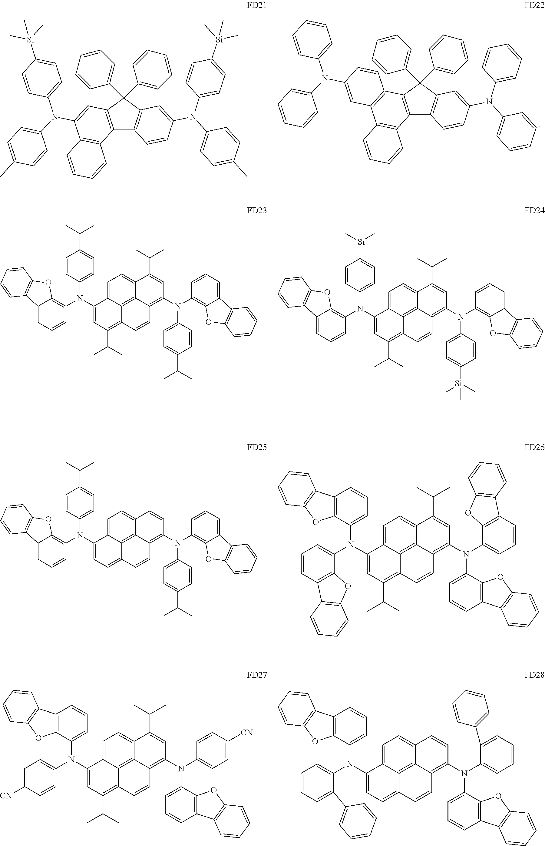


Delayed Fluorescence Material


[Ar601]xe11-[(L601)xe1-R601]xe21 Formula 601
wherein, in Formula 601,
-
- Ar601 and L601 may each independently be a C3-C60 carbocyclic group unsubstituted or substituted with at least one R10a or a C1-C60 heterocyclic group unsubstituted or substituted with at least one R10a,
- xe11 may be 1, 2, or 3,
- xe1 may be 0, 1, 2, 3, 4, or 5,
- R601 may be a C3-C60 carbocyclic group unsubstituted or substituted with at least one R10a, a C1-C60 heterocyclic group unsubstituted or substituted with at least one R10a, —Si(Q601)(Q602)(Q603), —C(═O)(Q601), —S(═O)2(Q601), or —P(═O)(Q601)(Q602), Q601 to Q603 may each be the same as described in connection with Q1,
- xe21 may be 1, 2, 3, 4, or 5, and
- at least one of Ar601, L601, and R601 may each independently be a π electron-deficient nitrogen-containing C1-C60 cyclic group unsubstituted or substituted with at least one R10a.

wherein, in Formula 601-1,
-
- X614 may be N or C(R614), X615 may be N or C(R615), X616 may be N or C(R616), and at least one of X614 to X616 may be N,
- L611 to L613 may each be the same as described in connection with L601,
- xe611 to xe613 may each be the same as described in connection with xe1,
- R611 to R613 may each be the same as described in connection with R601, and
- R614 to R116 may each independently be hydrogen, deuterium, —F, —Cl, —Br, —I, a hydroxyl group, a cyano group, a nitro group, a C1-C20 alkyl group, a C1-C20 alkoxy group, a C3-C60 carbocyclic group unsubstituted or substituted with at least one R10a, or a C1-C60 heterocyclic group unsubstituted or substituted with at least one R10a.


Electronic Apparatus
-
- the C3-C60 carbocyclic group may be i) a group T1, or ii) a condensed cyclic group in which two or more groups T1 are condensed with each other, for example, a cyclopentadiene group, an adamantane group, a norbornane group, a benzene group, a pentalene group, a naphthalene group, an azulene group, an indacene group, acenaphthylene group, a phenalene group, a phenanthrene group, an anthracene group, a fluoranthene group, a triphenylene group, a pyrene group, a chrysene group, a perylene group, a pentaphene group, a heptalene group, a naphthacene group, a picene group, a hexacene group, a pentacene group, a rubicene group, a coronene group, an ovalene group, an indene group, a fluorene group, a spiro-bifluorene group, a benzofluorene group, an indenophenanthrene group, or an indenoanthracene group, the C1-C60 heterocyclic group may be i) a group T2, ii) a condensed cyclic group in which two or more groups T2 are condensed with each other, or iii) a condensed cyclic group in which at least one group T2 and at least one group T1 are condensed with each other, for example, a pyrrole group, a thiophene group, a furan group, an indole group, a benzoindole group, a naphthoindole group, an isoindole group, a benzoisoindole group, a naphthoisoindole group, a benzosilole group, a benzothiophene group, a benzofuran group, a carbazole group, a dibenzosilole group, a dibenzothiophene group, a dibenzofuran group, an indenocarbazole group, an indolocarbazole group, a benzofurocarbazole group, a benzothienocarbazole group, a benzosilolocarbazole group, a benzoindolocarbazole group, a benzocarbazole group, a benzonaphthofuran group, a benzonaphthothiophene group, a benzonaphthosilole group, a benzofurodibenzofuran group, a benzofurodibenzothiophene group, a benzothienodibenzothiophene group, a pyrazole group, an imidazole group, a triazole group, an oxazole group, an isoxazole group, an oxadiazole group, a thiazole group, an isothiazole group, a thiadiazole group, a benzopyrazole group, a benzimidazole group, a benzoxazole group, a benzisoxazole group, a benzothiazole group, a benzisothiazole group, a pyridine group, a pyrimidine group, a pyrazine group, a pyridazine group, a triazine group, a quinoline group, an isoquinoline group, a benzoquinoline group, a benzoisoquinoline group, a quinoxaline group, a benzoquinoxaline group, a quinazoline group, a benzoquinazoline group, a phenanthroline group, a cinnoline group, a phthalazine group, a naphthyridine group, an imidazopyridine group, an imidazopyrimidine group, an imidazotriazine group, an imidazopyrazine group, an imidazopyridazine group, an azacarbazole group, an azafluorene group, an azadibenzosilole group, an azadibenzothiophene group, or an azadibenzofuran group,
- the π electron-rich C3-C60 cyclic group may be i) a group T1, ii) a condensed cyclic group in which two or more groups T1 are condensed with each other, iii) a group T3, iv) a condensed cyclic group in which two or more groups T3 are condensed with each other, or v) a condensed cyclic group in which at least one group T3 and at least one group T1 are condensed with each other, for example, a C3-C60 carbocyclic group, a pyrrole group, a thiophene group, a furan group, an indole group, a benzoindole group, a naphthoindole group, an isoindole group, a benzoisoindole group, a naphthoisoindole group, a benzosilole group, a benzothiophene group, a benzofuran group, a carbazole group, a dibenzosilole group, a dibenzothiophene group, a dibenzofuran group, an indenocarbazole group, an indolocarbazole group, a benzofurocarbazole group, a benzothienocarbazole group, a benzosilolocarbazole group, a benzoindolocarbazole group, a benzocarbazole group, a benzonaphthofuran group, a benzonaphthothiophene group, a benzonaphthosilole group, a benzofurodibenzofuran group, a benzofurodibenzothiophene group, or a benzothienodibenzothiophene group,
- the π electron-deficient nitrogen-containing C1-C60 cyclic group may be i) a group T4, ii) a condensed cyclic group in which two or more groups T4 are condensed with each other, iii) a condensed cyclic group in which at least one group T4 and at least one group T1 are condensed with each other, iv) a condensed cyclic group in which at least one group T4 and at least one group T3 are condensed with each other, or v) a condensed cyclic group in which at least one group T4, at least one group T1, and at least one group T3 are condensed with each other, for example, a pyrazole group, an imidazole group, a triazole group, an oxazole group, an isoxazole group, an oxadiazole group, a thiazole group, an isothiazole group, a thiadiazole group, a benzopyrazole group, a benzimidazole group, a benzoxazole group, a benzisoxazole group, a benzothiazole group, a benzisothiazole group, a pyridine group, a pyrimidine group, a pyrazine group, a pyridazine group, a triazine group, a quinoline group, an isoquinoline group, a benzoquinoline group, a benzoisoquinoline group, a quinoxaline group, a benzoquinoxaline group, a quinazoline group, a benzoquinazoline group, a phenanthroline group, a cinnoline group, a phthalazine group, a naphthyridine group, an imidazopyridine group, an imidazopyrimidine group, an imidazotriazine group, an imidazopyrazine group, an imidazopyridazine group, an azacarbazole group, an azafluorene group, an azadibenzosilole group, an azadibenzothiophene group, or an azadibenzofuran group,
- the group T1 may be a cyclopropane group, a cyclobutane group, a cyclopentane group, a cyclohexane group, a cycloheptane group, a cyclooctane group, a cyclobutene group, a cyclopentene group, a cyclopentadiene group, a cyclohexene group, a cyclohexadiene group, a cycloheptene group, an adamantane group, a norbornane group (or, a bicyclo[2.2.1]heptane group), a norbornene group, a bicyclo[1.1.1]pentane group, a bicyclo[2.1.1]hexane group, a bicyclo[2.2.2]octane group, or a benzene group,
- the group T2 may be a furan group, a thiophene group, a 1H-pyrrole group, a silole group, a borole group, a 2H-pyrrole group, a 3H-pyrrole group, an imidazole group, a pyrazole group, a triazole group, a tetrazole group, an oxazole group, an isoxazole group, an oxadiazole group, a thiazole group, an isothiazole group, a thiadiazole group, an azasilole group, an azaborole group, a pyridine group, a pyrimidine group, a pyrazine group, a pyridazine group, a triazine group, or a tetrazine group,
- the group T3 may be a furan group, a thiophene group, a 1H-pyrrole group, a silole group, or a borole group, and
- the group T4 may be a 2H-pyrrole group, a 3H-pyrrole group, an imidazole group, a pyrazole group, a triazole group, a tetrazole group, an oxazole group, an isoxazole group, an oxadiazole group, a thiazole group, an isothiazole group, a thiadiazole group, an azasilole group, an azaborole group, a pyridine group, a pyrimidine group, a pyrazine group, a pyridazine group, a triazine group, or a tetrazine group.
-
- deuterium, —F, —Cl, —Br, —I, a hydroxyl group, a cyano group, or a nitro group;
- a C1-C60 alkyl group, a C2-C60 alkenyl group, a C2-C60 alkynyl group, or a C1-C60 alkoxy group, each unsubstituted or substituted with deuterium, —F, —Cl, —Br, —I, a hydroxyl group, a cyano group, a nitro group, a C3-C60 carbocyclic group, a C1-C60 heterocyclic group, a C6-C60 aryloxy group, a C6-C60 arylthio group, —Si(Q11)(Q12)(Q13), —N(Q11)(Q12), —B(Q11)(Q12), —C(═O)(Q11), —S(═O)2(Q11), —P(═O)(Q11)(Q12), or a combination thereof;
- a C3-C60 carbocyclic group, a C1-C60 heterocyclic group, a C6-C60 aryloxy group, or a C6-C60 arylthio group, each unsubstituted or substituted with deuterium, —F, —Cl, —Br, —I, a hydroxyl group, a cyano group, a nitro group, a C1-C60 alkyl group, a C2-C60 alkenyl group, a C2-C60 alkynyl group, a C1-C60 alkoxy group, a C3-C60 carbocyclic group, a C1-C60 heterocyclic group, a C6-C60 aryloxy group, a C6-C60 arylthio group, —Si(Q21)(Q22)(Q23), —N(Q21)(Q22), —B(Q21)(Q22), —C(═O)(Q21), —S(═O)2(Q21), —P(═O)(Q21)(Q22), or a combination thereof; or
- —Si(Q31)(Q32)(Q33), —N(Q31)(Q32), —B(Q31)(Q32), —C(═O)(Q31), —S(═O)2(Q31), or —P(═O)(Q31)(Q32).

| TABLE 1 | ||
| EQE (%) | T95 (hr) | |
| Comparative Example 1 | 18.0 | 40 | |
| Comparative Example 2 | 19.8 | 55 | |
| Comparative Example 3 | 19.8 | 70 | |
| Example 1 | 19.5 | 80 | |
| Example 2 | 18.9 | 95 | |
| Comparative Example 4 | 18.2 | 45 | |
| Comparative Example 5 | 18.5 | 55 | |
| Comparative Example 6 | 17.5 | 48 | |
| Comparative Example 7 | 16.5 | 60 | |
| TABLE 2 | ||
| HOMO (eV) | LUMO (eV) | |
| TCTA | −5.69 | −2.40 | |
| Compound 2-4 | −5.70 | −2.63 | |
| Compound 4-12 | −5.09 | −1.97 | |
| DF10 | −5.17 | −2.17 | |
Claims (20)

Applications Claiming Priority (2)
| Application Number | Priority Date | Filing Date | Title |
|---|---|---|---|
| KR1020200114861A KR102822919B1 (en) | 2020-09-08 | 2020-09-08 | Light emitting device and electronic apparatus comprising same |
| KR10-2020-0114861 | 2020-09-08 |
Publications (2)
| Publication Number | Publication Date |
|---|---|
| US20220077416A1 US20220077416A1 (en) | 2022-03-10 |
| US11832467B2 true US11832467B2 (en) | 2023-11-28 |
Family
ID=80461739
Family Applications (1)
| Application Number | Title | Priority Date | Filing Date |
|---|---|---|---|
| US17/223,952 Active 2042-02-22 US11832467B2 (en) | 2020-09-08 | 2021-04-06 | Light-emitting device and electronic apparatus including the same |
Country Status (3)
| Country | Link |
|---|---|
| US (1) | US11832467B2 (en) |
| KR (1) | KR102822919B1 (en) |
| CN (1) | CN114156417A (en) |
Cited By (2)
| Publication number | Priority date | Publication date | Assignee | Title |
|---|---|---|---|---|
| US12141659B2 (en) | 2022-03-16 | 2024-11-12 | Yeda Research And Development Co. Ltd. | Resource for quantum computing |
| US12159200B2 (en) | 2021-04-27 | 2024-12-03 | Yeda Research And Development Co. Ltd. | Photonic quantum computation with dirty photons |
Citations (5)
| Publication number | Priority date | Publication date | Assignee | Title |
|---|---|---|---|---|
| US20060158102A1 (en) * | 2004-12-01 | 2006-07-20 | Idemitsu Kosan Co., Ltd. | Organic electroluminescent device |
| US9142791B2 (en) | 2011-05-27 | 2015-09-22 | Universal Display Corporation | OLED having multi-component emissive layer |
| CN109817818A (en) | 2019-01-31 | 2019-05-28 | 云谷(固安)科技有限公司 | A kind of organic electroluminescence device and display device |
| KR20190143282A (en) | 2018-06-20 | 2019-12-30 | 삼성전자주식회사 | Organic light emitting device |
| US20200052226A1 (en) | 2018-08-07 | 2020-02-13 | Lg Display Co., Ltd. | Organic Light Emitting Diode and Organic Light Emitting Device Having the Same |
Family Cites Families (6)
| Publication number | Priority date | Publication date | Assignee | Title |
|---|---|---|---|---|
| JP4753758B2 (en) * | 1998-05-01 | 2011-08-24 | Tdk株式会社 | Compound for organic EL device and organic EL device |
| JP2008270557A (en) * | 2007-04-20 | 2008-11-06 | Idemitsu Kosan Co Ltd | Organic EL device |
| JP6080415B2 (en) * | 2012-07-19 | 2017-02-15 | キヤノン株式会社 | White organic EL element, lighting device and display device using the same |
| KR102354847B1 (en) * | 2014-12-16 | 2022-01-24 | 엘지디스플레이 주식회사 | Organic light emitting display device |
| KR20190067694A (en) * | 2017-12-07 | 2019-06-17 | 삼성전자주식회사 | Organic light emitting device |
| CN109411633B (en) * | 2018-08-31 | 2020-12-15 | 昆山国显光电有限公司 | An organic electroluminescent device and its preparation method and display device |
-
2020
- 2020-09-08 KR KR1020200114861A patent/KR102822919B1/en active Active
-
2021
- 2021-04-06 US US17/223,952 patent/US11832467B2/en active Active
- 2021-06-29 CN CN202110724924.6A patent/CN114156417A/en active Pending
Patent Citations (8)
| Publication number | Priority date | Publication date | Assignee | Title |
|---|---|---|---|---|
| US20060158102A1 (en) * | 2004-12-01 | 2006-07-20 | Idemitsu Kosan Co., Ltd. | Organic electroluminescent device |
| US9142791B2 (en) | 2011-05-27 | 2015-09-22 | Universal Display Corporation | OLED having multi-component emissive layer |
| KR101699583B1 (en) | 2011-05-27 | 2017-02-13 | 유니버셜 디스플레이 코포레이션 | Oled having multi-component emissivie layer |
| KR20190143282A (en) | 2018-06-20 | 2019-12-30 | 삼성전자주식회사 | Organic light emitting device |
| US20200006676A1 (en) | 2018-06-20 | 2020-01-02 | Samsung Electronics Co., Ltd. | Organic light-emitting device |
| US20200052226A1 (en) | 2018-08-07 | 2020-02-13 | Lg Display Co., Ltd. | Organic Light Emitting Diode and Organic Light Emitting Device Having the Same |
| KR20200016538A (en) | 2018-08-07 | 2020-02-17 | 엘지디스플레이 주식회사 | Organic light emitting diode and organic light emitting device having the diode |
| CN109817818A (en) | 2019-01-31 | 2019-05-28 | 云谷(固安)科技有限公司 | A kind of organic electroluminescence device and display device |
Non-Patent Citations (2)
| Title |
|---|
| Si Hyun Han et al., "Spatial separation of sensitizer and fluorescent emitter for high quantum efficiency in hyperfluorescent organic light-emitting diodes," Journal of Materials Chemistry C, Jan. 11, 2018, pp. 1-21, DOI: 10.1039/C7TC05283A. |
| Yifan Zhang et al., "Tenfold increase in the lifetime of blue phosphorescent organic light-emitting diodes," Nature Communications, Sep. 25, 2014, pp. 1-7, DOI: 10.1038/ncomms6008. |
Cited By (6)
| Publication number | Priority date | Publication date | Assignee | Title |
|---|---|---|---|---|
| US12159200B2 (en) | 2021-04-27 | 2024-12-03 | Yeda Research And Development Co. Ltd. | Photonic quantum computation with dirty photons |
| US12190205B2 (en) | 2021-04-27 | 2025-01-07 | Yeda Research And Development Co. Ltd. | Heralding-free connections in quantum computing |
| US12198012B2 (en) | 2021-04-27 | 2025-01-14 | Yeda Research And Development Co. Ltd. | N-configuration resonator-coupled quantum emitter |
| US12555020B2 (en) * | 2021-04-27 | 2026-02-17 | Quantum Source Labs Ltd. | Entangling photonic graphs |
| US12141659B2 (en) | 2022-03-16 | 2024-11-12 | Yeda Research And Development Co. Ltd. | Resource for quantum computing |
| US12190206B2 (en) | 2022-03-16 | 2025-01-07 | Yeda Research And Development Co. Ltd. | Detectors, optical switches, and waveguides |
Also Published As
| Publication number | Publication date |
|---|---|
| KR20220033610A (en) | 2022-03-17 |
| CN114156417A (en) | 2022-03-08 |
| US20220077416A1 (en) | 2022-03-10 |
| KR102822919B1 (en) | 2025-06-20 |
Similar Documents
| Publication | Publication Date | Title |
|---|---|---|
| US20230329103A1 (en) | Light-emitting device and electronic apparatus including the same | |
| US20220246856A1 (en) | Light-emitting diode and electronic device including the same | |
| US12035621B2 (en) | Light-emitting device and electronic apparatus including the same | |
| US20220045293A1 (en) | Light-emitting device and electronic apparatus including the same | |
| US20260040816A1 (en) | Heterocyclic compound, light-emitting device including the same, and electronic apparatus including the light-emitting device | |
| US20230268467A1 (en) | Light-emitting device and electronic apparatus including light-emitting device | |
| US11832467B2 (en) | Light-emitting device and electronic apparatus including the same | |
| US12358883B2 (en) | Light-emitting device and electronic apparatus including the same | |
| US11950499B2 (en) | Light-emitting device comprising first and second capping layers and electronic apparatus including the same | |
| US20220037606A1 (en) | Light-emitting device and electronic apparatus including the same | |
| US20210408387A1 (en) | Light-emitting device and electronic apparatus including same | |
| US20220052276A1 (en) | Light-emitting device and electronic apparatus including the same | |
| US20230165022A1 (en) | Light-emitting device and electronic apparatus including the same | |
| US12559477B2 (en) | Light-emitting device including heterocyclic compound and electronic apparatus including the light-emitting device | |
| US12410130B2 (en) | Light-emitting device and electronic apparatus including the same | |
| US20220006028A1 (en) | Light-emitting device and electronic apparatus including the light-emitting device | |
| US20220149293A1 (en) | Organic light-emitting device and electronic apparatus including the same | |
| US20220059793A1 (en) | Light-emitting device and electronic apparatus including the same | |
| US12356792B2 (en) | Light-emitting device and electronic apparatus including the same | |
| US12484372B2 (en) | Light-emitting device and electronic apparatus including the same | |
| US12317742B2 (en) | Light-emitting device and electronic apparatus including the same | |
| US12514112B2 (en) | Light-emitting device and electronic apparatus including the same | |
| US12486421B2 (en) | Ink composition for light-emitting device and light emitting device manufactured using same | |
| US20220320436A1 (en) | Light-emitting device and electronic apparatus including the same | |
| US20230171984A1 (en) | Light-emitting device and electronic apparatus including the same |
Legal Events
| Date | Code | Title | Description |
|---|---|---|---|
| FEPP | Fee payment procedure |
Free format text: ENTITY STATUS SET TO UNDISCOUNTED (ORIGINAL EVENT CODE: BIG.); ENTITY STATUS OF PATENT OWNER: LARGE ENTITY |
|
| AS | Assignment |
Owner name: SAMSUNG DISPLAY CO., LTD., KOREA, REPUBLIC OF Free format text: ASSIGNMENT OF ASSIGNORS INTEREST;ASSIGNORS:SHIN, HYOSUP;NAIJO, TSUYOSHI;KIM, HYUNYOUNG;AND OTHERS;REEL/FRAME:055852/0259 Effective date: 20210330 |
|
| STPP | Information on status: patent application and granting procedure in general |
Free format text: DOCKETED NEW CASE - READY FOR EXAMINATION |
|
| STPP | Information on status: patent application and granting procedure in general |
Free format text: RESPONSE TO NON-FINAL OFFICE ACTION ENTERED AND FORWARDED TO EXAMINER |
|
| STPP | Information on status: patent application and granting procedure in general |
Free format text: NOTICE OF ALLOWANCE MAILED -- APPLICATION RECEIVED IN OFFICE OF PUBLICATIONS |
|
| STPP | Information on status: patent application and granting procedure in general |
Free format text: PUBLICATIONS -- ISSUE FEE PAYMENT VERIFIED |
|
| STCF | Information on status: patent grant |
Free format text: PATENTED CASE |