US11817841B2 - Adaptive capacitive filter circuit - Google Patents
Adaptive capacitive filter circuit Download PDFInfo
- Publication number
- US11817841B2 US11817841B2 US17/573,579 US202217573579A US11817841B2 US 11817841 B2 US11817841 B2 US 11817841B2 US 202217573579 A US202217573579 A US 202217573579A US 11817841 B2 US11817841 B2 US 11817841B2
- Authority
- US
- United States
- Prior art keywords
- switch
- filter circuit
- capacitive filter
- coupled
- circuit
- Prior art date
- Legal status (The legal status is an assumption and is not a legal conclusion. Google has not performed a legal analysis and makes no representation as to the accuracy of the status listed.)
- Active, expires
Links
Images

Classifications
-
- H—ELECTRICITY
- H03—ELECTRONIC CIRCUITRY
- H03H—IMPEDANCE NETWORKS, e.g. RESONANT CIRCUITS; RESONATORS
- H03H19/00—Networks using time-varying elements, e.g. N-path filters
- H03H19/004—Switched capacitor networks
-
- G—PHYSICS
- G01—MEASURING; TESTING
- G01R—MEASURING ELECTRIC VARIABLES; MEASURING MAGNETIC VARIABLES
- G01R19/00—Arrangements for measuring currents or voltages or for indicating presence or sign thereof
- G01R19/165—Indicating that current or voltage is either above or below a predetermined value or within or outside a predetermined range of values
- G01R19/16533—Indicating that current or voltage is either above or below a predetermined value or within or outside a predetermined range of values characterised by the application
- G01R19/16538—Indicating that current or voltage is either above or below a predetermined value or within or outside a predetermined range of values characterised by the application in AC or DC supplies
-
- H—ELECTRICITY
- H02—GENERATION; CONVERSION OR DISTRIBUTION OF ELECTRIC POWER
- H02M—APPARATUS FOR CONVERSION BETWEEN AC AND AC, BETWEEN AC AND DC, OR BETWEEN DC AND DC, AND FOR USE WITH MAINS OR SIMILAR POWER SUPPLY SYSTEMS; CONVERSION OF DC OR AC INPUT POWER INTO SURGE OUTPUT POWER; CONTROL OR REGULATION THEREOF
- H02M1/00—Details of apparatus for conversion
- H02M1/10—Arrangements incorporating converting means for enabling loads to be operated at will from different kinds of power supplies, e.g. from AC or DC
-
- H—ELECTRICITY
- H02—GENERATION; CONVERSION OR DISTRIBUTION OF ELECTRIC POWER
- H02M—APPARATUS FOR CONVERSION BETWEEN AC AND AC, BETWEEN AC AND DC, OR BETWEEN DC AND DC, AND FOR USE WITH MAINS OR SIMILAR POWER SUPPLY SYSTEMS; CONVERSION OF DC OR AC INPUT POWER INTO SURGE OUTPUT POWER; CONTROL OR REGULATION THEREOF
- H02M1/00—Details of apparatus for conversion
- H02M1/14—Arrangements for reducing ripples from DC input or output
- H02M1/15—Arrangements for reducing ripples from DC input or output using active elements
-
- H—ELECTRICITY
- H02—GENERATION; CONVERSION OR DISTRIBUTION OF ELECTRIC POWER
- H02M—APPARATUS FOR CONVERSION BETWEEN AC AND AC, BETWEEN AC AND DC, OR BETWEEN DC AND DC, AND FOR USE WITH MAINS OR SIMILAR POWER SUPPLY SYSTEMS; CONVERSION OF DC OR AC INPUT POWER INTO SURGE OUTPUT POWER; CONTROL OR REGULATION THEREOF
- H02M1/00—Details of apparatus for conversion
- H02M1/32—Means for protecting converters other than automatic disconnection
-
- H—ELECTRICITY
- H02—GENERATION; CONVERSION OR DISTRIBUTION OF ELECTRIC POWER
- H02M—APPARATUS FOR CONVERSION BETWEEN AC AND AC, BETWEEN AC AND DC, OR BETWEEN DC AND DC, AND FOR USE WITH MAINS OR SIMILAR POWER SUPPLY SYSTEMS; CONVERSION OF DC OR AC INPUT POWER INTO SURGE OUTPUT POWER; CONTROL OR REGULATION THEREOF
- H02M3/00—Conversion of DC power input into DC power output
- H02M3/02—Conversion of DC power input into DC power output without intermediate conversion into AC
- H02M3/04—Conversion of DC power input into DC power output without intermediate conversion into AC by static converters
- H02M3/10—Conversion of DC power input into DC power output without intermediate conversion into AC by static converters using discharge tubes with control electrode or semiconductor devices with control electrode
- H02M3/145—Conversion of DC power input into DC power output without intermediate conversion into AC by static converters using discharge tubes with control electrode or semiconductor devices with control electrode using devices of a triode or transistor type requiring continuous application of a control signal
- H02M3/155—Conversion of DC power input into DC power output without intermediate conversion into AC by static converters using discharge tubes with control electrode or semiconductor devices with control electrode using devices of a triode or transistor type requiring continuous application of a control signal using semiconductor devices only
- H02M3/156—Conversion of DC power input into DC power output without intermediate conversion into AC by static converters using discharge tubes with control electrode or semiconductor devices with control electrode using devices of a triode or transistor type requiring continuous application of a control signal using semiconductor devices only with automatic control of output voltage or current, e.g. switching regulators
-
- H—ELECTRICITY
- H02—GENERATION; CONVERSION OR DISTRIBUTION OF ELECTRIC POWER
- H02M—APPARATUS FOR CONVERSION BETWEEN AC AND AC, BETWEEN AC AND DC, OR BETWEEN DC AND DC, AND FOR USE WITH MAINS OR SIMILAR POWER SUPPLY SYSTEMS; CONVERSION OF DC OR AC INPUT POWER INTO SURGE OUTPUT POWER; CONTROL OR REGULATION THEREOF
- H02M7/00—Conversion of AC power input into DC power output; Conversion of DC power input into AC power output
- H02M7/02—Conversion of AC power input into DC power output without possibility of reversal
- H02M7/04—Conversion of AC power input into DC power output without possibility of reversal by static converters
-
- H—ELECTRICITY
- H03—ELECTRONIC CIRCUITRY
- H03H—IMPEDANCE NETWORKS, e.g. RESONANT CIRCUITS; RESONATORS
- H03H11/00—Networks using active elements
- H03H11/02—Multiple-port networks
- H03H11/04—Frequency selective two-port networks
-
- H—ELECTRICITY
- H03—ELECTRONIC CIRCUITRY
- H03H—IMPEDANCE NETWORKS, e.g. RESONANT CIRCUITS; RESONATORS
- H03H19/00—Networks using time-varying elements, e.g. N-path filters
- H03H19/002—N-path filters
-
- H—ELECTRICITY
- H03—ELECTRONIC CIRCUITRY
- H03K—PULSE TECHNIQUE
- H03K5/00—Manipulating of pulses not covered by one of the other main groups of this subclass
- H03K5/22—Circuits having more than one input and one output for comparing pulses or pulse trains with each other according to input signal characteristics, e.g. slope, integral
- H03K5/24—Circuits having more than one input and one output for comparing pulses or pulse trains with each other according to input signal characteristics, e.g. slope, integral the characteristic being amplitude
-
- H—ELECTRICITY
- H02—GENERATION; CONVERSION OR DISTRIBUTION OF ELECTRIC POWER
- H02M—APPARATUS FOR CONVERSION BETWEEN AC AND AC, BETWEEN AC AND DC, OR BETWEEN DC AND DC, AND FOR USE WITH MAINS OR SIMILAR POWER SUPPLY SYSTEMS; CONVERSION OF DC OR AC INPUT POWER INTO SURGE OUTPUT POWER; CONTROL OR REGULATION THEREOF
- H02M1/00—Details of apparatus for conversion
- H02M1/14—Arrangements for reducing ripples from DC input or output
Definitions
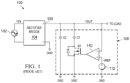
- FIG. 1 is a diagram of a conventional power management system 100 having an alternating-current (AC) source 102 , a rectifier bridge 104 , and a capacitive filter 108 .
- the rectifier bridge 104 is coupled to the AC source 102 and includes a rectifier bridge output 106 .
- the rectifier bridge 104 is configured to rectify an input voltage (VIN) from the AC source 102 , resulting in an output voltage (VOUT) at the rectifier bridge output 106 .
- VOUT is provided to a load (not shown).
- the capacitive filter 108 is configured to support two different VIN levels (e.g., 120V and 240V). As shown, the capacitive filter 108 includes a first capacitor (C 1 ) and a second capacitor (C 2 ). C 2 has a first electrode coupled to the rectifier bridge output 106 and a second electrode coupled to ground. C 1 has a first electrode coupled to the rectifier bridge output 106 and a second electrode coupled to ground via a switch (Q 1 ). Q 1 is controlled by the output of a comparator 110 , which is configured to compare VOUT (proportional to VIN) with a reference voltage (VREF) provided by a voltage source 112 .
- VOUT proportional to VIN
- VREF reference voltage
- VOUT When VOUT is greater than VREF (e.g., above 190V), Q 1 is open, C 1 is disconnected, and C 2 (e.g., rated for 400V) is the only filter capacitor connected.
- VOUT When VOUT is not greater than VREF (e.g., not greater than 190V), Q 1 is closed, and C 1 (e.g., rated for 200V) is connected in parallel with C 2 .
- the power management system 100 has various shortcomings. Firstly, a short to Q 1 results in a hazardous overvoltage condition on C 1 . Secondly, Q 1 needs to withstand the peak VIN. Also, the minimum value of C 2 may be limited by the root r mean square (RMS) current rating rather than the energy storage requirements.
- RMS root r mean square
- an adaptive capacitive filter circuit includes: a first adaptive capacitive filter circuit terminal adapted to be coupled to a rectifier bridge output; a second adaptive capacitive filter circuit terminal adapted to be coupled to ground; a first capacitor having a first electrode and a second electrode, the first electrode of the first capacitor coupled to the first adaptive capacitive filter circuit terminal; a second capacitor having a first electrode and a second electrode, the second electrode of the second capacitor coupled to the second adaptive capacitive filter circuit terminal; a first switch coupled between the second electrode of the first capacitor and the second adaptive capacitive filter circuit terminal; a second switch coupled between the first adaptive capacitive filter circuit terminal and the first electrode of the second capacitor; and a third switch coupled between the second electrode of the first capacitor and the first electrode of the second capacitor.
- an integrated circuit includes control circuitry for an adaptive capacitive filter circuit.
- the control circuitry is configured to: detect whether an output voltage at a rectifier bridge output is greater than a threshold; responsive to detecting that the output voltage is greater than the threshold, provide a first set of switch drive signals for switches of the adaptive capacitive filter circuit to couple capacitors of the adaptive capacitive filter circuit in series; and responsive to detecting that the output voltage is not greater than the threshold, provide a second set of switch drive signals for switches of the adaptive capacitive filter circuit to couple the capacitors of the adaptive capacitive filter circuit in parallel.
- a system in yet another example embodiment, includes an adaptive capacitive filter circuit having: a set of capacitors; a first adaptive capacitive filter circuit terminal adapted to be coupled to a rectifier bridge output; and a second adaptive capacitive filter circuit terminal adapted to be coupled to ground.
- the adaptive capacitive filter circuit is configured to connect capacitors of the set of capacitors in series or in parallel between the first adaptive capacitive filter circuit terminal and the second adaptive capacitive filter circuit terminal responsive to a control signal.
- FIG. 1 is a diagram of a conventional power management system having a capacitive filter.
- FIG. 2 is a diagram of a power management system having an adaptive capacitive filter circuit in accordance with an example embodiment.
- FIG. 3 is a diagram of another power management system having an adaptive capacitive filter circuit in accordance with an example embodiment.
- FIG. 4 is a diagram of a system having an adaptive capacitive filter circuit in accordance with an example embodiment.
- FIG. 5 is a flowchart of an adaptive capacitive filter circuit method in accordance with an example embodiment.
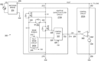
- FIG. 2 is a diagram of a power management system 200 having an adaptive capacitive filter circuit 210 in accordance with an example embodiment.
- the power management system 200 includes an alternating-current (AC) source 202 coupled to a rectifier bridge 204 having a rectifier bridge output 206 .
- the rectifier bridge 204 is configured to rectify an input voltage (VIN) from the AC source 202 , resulting in an output voltage (VOUT) at the rectifier bridge output 206 , where VOUT is smoothed by the adaptive capacitive filter circuit 210 .
- VIN input voltage
- VOUT output voltage
- the rectifier bridge output 206 is adapted to be coupled to a load, the adaptive capacitive filter circuit 210 , and a control circuit 250 for the adaptive capacitive filter circuit 210 .
- the adaptive capacitive filter circuit 210 and the control circuit 250 are configured to adjust a capacitive filter value at the rectifier bridge output 206 to account for two or more possible VIN levels (e.g., 120V and 240V) from the AC source 202 while protecting against possible fault conditions.
- the control circuit 250 is part of the adaptive capacitive filter circuit 210 rather than separate from and coupled to the adaptive capacitive filter circuit 210 .
- the adaptive capacitive filter circuit 210 includes a first adaptive capacitive filter circuit terminal 212 , a second adaptive capacitive filter circuit terminal 214 , and a third adaptive capacitive filter circuit terminal 216 .
- the first adaptive capacitive filter circuit terminal 212 is coupled to the rectifier bridge output 206 and is configured to receive VOUT.
- the second adaptive capacitive filter circuit terminal 214 is coupled to a control circuit output 254 of the control circuit 250 and is configured to receive a control signal (CS 1 ) that indicates whether VOUT is greater than a threshold.
- the third adaptive capacitive filter circuit terminal 216 is coupled to ground.
- the control circuit 250 includes a control circuit input 252 , the control circuit output 254 , and a control circuit terminal 256 .
- the control circuit input 252 is coupled to the rectifier bridge output 206 and is configured to receive VOUT.
- the control circuit terminal 256 is coupled to ground.
- the control circuit 250 is configured to provide CS 1 at the control circuit output 254 responsive to a comparison of VOUT with a threshold (e.g., the value of CS 1 varies depending on whether VOUT is greater than the threshold).
- the adaptive capacitive filter circuit 210 includes a set of capacitors 218 having a first set of capacitors terminal 220 and a second set of capacitors terminal 222 .
- the first set of capacitors terminal 220 is coupled to the first adaptive capacitive filter circuit terminal 212 .
- the second set of capacitors terminal 222 is coupled to the switch arrangement 224 .
- the switch arrangement 224 includes a first switch arrangement terminal 226 , a second switch arrangement terminal 228 , a third switch arrangement terminal 230 , and a fourth switch arrangement terminal 232 .
- the first switch arrangement terminal 226 is coupled to the second set of capacitors terminal 222 .
- the second switch arrangement terminal 228 is coupled to the control circuit output 254 .
- the third switch arrangement terminal 230 is coupled to ground via the third adaptive capacitive filter circuit terminal 216 .
- the fourth switch arrangement terminal 232 is coupled to a fault sense circuit 240 .
- the fault sense circuit 240 includes a first fault sense circuit input 242 , a second fault sense circuit input 244 , and a fault sense circuit output 246 .
- the first fault sense circuit input 242 is coupled to the first set of capacitors terminal 220 .
- the second fault sense circuit input 244 is coupled to the second set of capacitors terminal 222 .
- the fault sense circuit output 246 is coupled to the fourth switch arrangement terminal 232 .
- the fault sense circuit 240 is configured to provide a control signal (CS 2 ) at the fault sense circuit output 246 responsive to sense signals received at the first fault sense circuit input 242 and the second fault sense circuit input 244 .
- the fault sense circuit 240 may include respective inputs to sense faults for any capacitor of the set of capacitors 218 and/or any switch of the switch arrangement 224 .
- the control circuit 250 is configured to provide CS 1 at the control circuit output 254 based on a comparison of VOUT with a threshold.
- the switch arrangement 224 is configured to provide a parallel connection option 234 for capacitors of the set of capacitors 218 or a series connection option 236 for capacitors of the set of capacitors 218 .
- CS 1 directs the switch arrangement 224 to use the series connection option 236 for capacitors of the set of capacitors 218 .
- VOUT is not above the threshold
- CS 1 directs the switch arrangement 224 to use the parallel connection option 234 for capacitors of the set of capacitors 218 .
- the set of capacitors 212 includes a first capacitor and a second capacitors that are coupled in series or in parallel based on the switch arrangement 214 and responsive to CS 1 .
- a fault condition (e.g., a capacitor fault and/or a switch fault) related to the adaptive capacitive filter circuit 210 may be detected. Responsive to a detected fault condition, the fault sense circuit 240 is configured to provide CS 2 to the fourth switch arrangement terminal 232 of the switch arrangement 224 . Responsive to CS 2 , the switch arrangement 224 is configured to use a fault option 238 for switches of the switch arrangement 224 . In some example embodiments, the fault option 238 assumes switches of the switch arrangement 224 will fault to a short circuit rather than an open circuit.
- the fault option 238 provides a path to ground (e.g., by connecting the first adaptive capacitive filter circuit terminal 212 to the third adaptive capacitive filter circuit 216 via switches of the switch arrangement 224 ) so that a fuse will trigger responsive to the detected fault condition.
- the fuse (not shown) may be between the AC source 202 and the rectifier bridge 204 .
- the switch arrangement 224 includes control logic (e.g., the control logic 320 in FIGS. 3 and 4 ) configured to receive CS 1 and CS 2 and provide switch control signals responsive to CS 1 and CS 2 . When CS 2 indicates a fault condition, CS 2 has priority over CS 1 .
- control circuit 250 the fault sense circuit 240 , and such control logic form the control circuitry for the adaptive capacitive filter circuit 210 .
- control circuitry for the adaptive capacitive filter circuit 210 may be part of one integrated circuit (IC) or multiple ICs.
- the switch arrangement 224 may be included with the same IC as the control circuitry.
- the set of capacitors 218 may be separate from the IC or ICs having the control circuitry and the switch arrangement 224 .
- adaptive capacitive filter circuit 210 With the adaptive capacitive filter circuit 210 and the control circuit 250 , different VIN levels from the AC source 202 are supported while reducing the shortcomings of the conventional approach of FIG. 1 .
- Some benefits of the adaptive capacitive filter circuit 210 relative to the conventional approach of FIG. 1 include accounting for fault conditions and using capacitors with smaller ratings. Compared to Q 1 in FIG. 1 , the switches of the switch arrangement 224 have smaller ratings and are physically smaller.
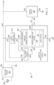
- FIG. 3 is a diagram of another power management system 300 having an adaptive capacitive filter circuit 210 A (an example of the adaptive capacitive filter circuit 210 in FIG. 2 ) in accordance with an example embodiment.
- the power management system 300 includes the AC source 202 coupled to the rectifier bridge 204 .
- the rectifier bridge output 206 of the rectifier bridge 204 is coupled to the adaptive capacitive filter circuit 210 A and a control circuit 250 A (an example of the control circuit 250 in FIG. 1 ).
- the rectifier bridge output 206 is adapted to be coupled to load (not shown).
- the rectifier bridge 204 is configured to rectify VIN from the AC source 202 , resulting in VOUT at the rectifier bridge output 206 , where VOUT is a smoothed by the adaptive capacitive filter circuit 210 A.
- the adaptive capacitive filter circuit 210 A and the control circuit 250 A are configured to adjust a capacitive filter value at the rectifier bridge output 206 to account for two VIN levels (e.g., 120V and 240V) while protecting against possible fault conditions.
- the control circuit 250 A is part of the adaptive capacitive filter circuit 210 A rather than coupled to the adaptive capacitive filter circuit 210 A.
- the adaptive capacitive filter circuit 210 A includes the first adaptive capacitive filter circuit terminal 212 , the second adaptive capacitive filter circuit terminal 214 , and the third adaptive capacitive filter circuit terminal 216 .
- the first adaptive capacitive filter circuit terminal 212 is coupled to the rectifier bridge output 206 and is configured to receive VOUT.
- the second adaptive capacitive filter circuit terminal 214 is coupled to the control circuit output 254 of the control circuit 250 A and is configured to receive CS 1 .
- the third adaptive capacitive filter circuit terminal 216 is coupled to ground.
- the adaptive capacitive filter circuit 210 A includes capacitors C 3 and C 4 (an example of the set of capacitors 218 in FIG. 2 ).
- the adaptive capacitive filter circuit 210 A also includes transistors Q 2 , Q 3 , and Q 4 (e.g., switches of the switch arrangement 224 in FIG. 2 ).
- the adaptive capacitive filter circuit 210 A also includes a fault sense circuit 240 A (an example of the fault sense circuit 240 in FIG. 2 ) and control logic 320 .
- a first electrode of C 3 is coupled to the first adaptive capacitive filter circuit terminal 212 .
- a second electrode of C 3 is coupled to ground via Q 2 .
- a first current terminal of Q 2 is coupled to the second electrode of C 3
- a second current terminal of Q 2 is coupled to ground.
- a first electrode of C 4 is coupled to the first adaptive capacitive filter circuit terminal 212 via Q 3 .
- a first current terminal of Q 3 is coupled to the first adaptive capacitive filter circuit terminal 212
- a second current terminal of Q 3 is coupled to the first electrode of C 4 .
- a second electrode of C 4 is coupled to ground.
- the first electrode of C 4 is also coupled to the second electrode of C 3 via Q 4 .
- a first current terminal of Q 4 is coupled to the second electrode of C 3
- the second current terminal of Q 4 is coupled to the first electrode of C 4 .
- the control of Q 2 , Q 3 , and Q 4 is based on the operations of the control circuit 250 A, the fault sense circuit 240 A, and the control logic 320 .
- the control circuit 250 A includes a comparator 302 having an inverting input, a non-inverting input, and a comparator output 304 .
- the inverting input of the comparator 302 is coupled to the control circuit input 252 and is configured to receive VOUT (proportional to VIN).
- the non-inverting input of the comparator 302 is coupled to a voltage source 308 and is configured to receive reference voltage (VREF) from the voltage source 308 (i.e., VREF is a threshold).
- VREF reference voltage
- a first side of the voltage source 308 is coupled to the non-inverting input of the comparator 302 , and a second side of the voltage source 308 is coupled to ground via the control circuit terminal 256 .
- the comparator 302 is configured to adjust CS 1 at the comparator output 304 based on a comparison of VOUT with VREF.
- the fault sense circuit 240 A includes fault sense circuit inputs 310 configured to receive sense signals.
- the sense signals indicate, for example, the voltage across C 3 , the voltage across C 4 , the voltage across Q 3 , the voltage across Q 4 , the voltage across Q 5 , and/or other sense signals.
- current sense signals could indicate a fault condition.
- the faults sense circuit 240 A is configured to adjust CS 2 at the fault sense circuit output 246 to indicate whether there are any faults.
- CS 1 and CS 2 are provided to the control logic 320 as inputs. More specifically, the control logic 320 includes a first control logic input 322 , a second control logic input 324 , a first control logic output 326 , and a second control logic output 328 .
- the first control logic input 322 is configured to receive CS 1 .
- the second control logic input 324 is configured to receive CS 2 .
- the first control logic output 326 is coupled to the control terminals of Q 2 and Q 3 .
- the second control logic output 328 is coupled to the control terminal of Q 4 .
- the control logic 320 is configured to provide switch control signals for Q 2 , Q 3 , and Q 4 response to CS 1 and CS 2 .
- the control logic 320 is configured to provide switch control signals so that C 3 and C 4 are in series (i.e., Q 2 and Q 3 off, and Q 4 on) between the first adaptive capacitive filter circuit terminal 212 and ground. If CS 1 is a second value (indicating VOUT is not greater than VREF), the control logic 320 is configured to provide switch control signals so that C 3 and C 4 are in parallel (i.e., Q 2 and Q 3 on, and Q 4 off) between the first adaptive capacitive filter circuit terminal 212 and ground.
- the control logic 320 is configured to provide switch control signals so that C 3 and C 4 are bypassed such that the first adaptive capacitive filter circuit terminal 212 is coupled to ground via Q 2 , Q 3 , and Q 4 (i.e., Q 2 , Q 3 , and Q 4 on or shorted).
- CS 2 indicates a fault condition
- CS 2 has priority over CS 1 .
- the number of voltage levels supported, the number of capacitors, and the number of switches may vary from the example of FIG. 3
- control circuit 250 A, the fault sense circuit 240 A, and the control logic 320 form the control circuitry for the adaptive capacitive filter circuit 210 A.
- the control circuitry for the adaptive capacitive filter circuit 210 A may be part of one IC or multiple ICs.
- Q 2 , Q 3 , and Q 4 may be included with the same IC as the control circuitry.
- C 3 and C 4 may be separate from the IC or ICs having the control circuitry and Q 2 , Q 3 , and Q 4 .
- the adaptive capacitive filter circuit 210 A includes a first terminal 330 and a second terminal 332 .
- the first terminal 330 is between the second current terminal of Q 3 , the second current terminal of Q 4 , and the first electrode of C 4 .
- the second terminal 332 is between the second electrode of C 3 , the first current terminal of Q 2 and the first current terminal of Q 4 .
- the IC may include external terminals or pins related to the first terminal 330 and the second terminal 332 of the adaptive capacitive filter circuit 210 A to facilitate coupling C 3 and C 4 to the other components as shown in FIG. 3 .
- the IC may also include external terminals or pins related to the first adaptive capacitive filter circuit terminal 212 , and the third adaptive capacitive filter circuit terminal 216 .
- the control circuit 250 A is internal to the IC having the control logic 320 .
- the second adaptive capacitive filter circuit terminal 214 is an internal terminal of the IC rather than an external terminal or pin.
- all switches may be initially off (i.e., a cold start).
- an input voltage e.g., VIN from the AC source 202
- C 3 and C 4 charge in series through the body diode of Q 4 to a voltage that is approximately equal to one half the peak input voltage. Consequently, all the switches are exposed to a voltage not higher than half the input voltage.
- transistor e.g., Q 1
- the transistors of the adaptive capacitive filter circuit e.g., Q 2 , Q 3 , and Q 4
- the transistors of the adaptive capacitive filter circuit will be rated to a voltage that is half that of Q 1 .
- the result is a substantial decrease in the specific on-resistance (Rsp) and relative size of Q 2 , Q 3 , and Q 4 relative to Q 1 .
- C 3 and C 4 are rated for half the peak input voltage. With a lower rating for C 3 and C 4 , a substantially higher root mean square (RMS) current capability exists relative to C 1 and C 2 in the conventional approach. Also, capacitance of the adaptive capacitive filter circuit is constrained by energy storage requirements rather than RMS current.
- RMS root mean square
- failure of either Q 2 or Q 3 results in overvoltage on capacitors C 3 or C 4 .
- Capacitor failure of C 3 or C 4 may result in a fault current that may not be high enough to clear the input fuse resulting in catastrophic venting/fire risk.
- the voltage across C 1 and C 2 may be sensed. If the sense voltage exceeds a particular value, all switches (e.g., Q 2 , Q 3 , and Q 4 in FIG. 3 ) are turned on simultaneously, thereby “crowbarring” the output of the bridge rectifier and creating a fault current sufficient to clear the input fuse.
- the voltage across Q 2 , Q 3 , or Q 4 may be sensed to detect a fault condition.
- adaptive capacitive filter circuit 210 A and the control circuit 250 A With the adaptive capacitive filter circuit 210 A and the control circuit 250 A, different VIN levels from the AC source 202 are supported while reducing the shortcomings of the conventional approach of FIG. 1 .
- Some benefits of the adaptive capacitive filter circuit 210 A relative to the conventional approach of FIG. 1 include accounting for fault conditions and using capacitors with smaller ratings. Compared to Q 1 in FIG. 1 , Q 2 , Q 3 , and Q 4 in FIG. 3 have smaller ratings and are physically smaller.
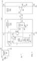
- FIG. 4 is a diagram of a system 400 having an adaptive capacitive filter circuit 210 B in accordance with an example embodiment.
- the system 400 represents any electrical device having a load 430 and power management circuitry including: a power supply 401 ; the adaptive capacitive filter circuit 210 B; a power stage 410 ; and switching converter controller components for the power stage 410 .
- the control circuitry e.g., the control circuit 250 , the control logic 320 , and the fault sense circuit 240 A
- the switch arrangement 224 of the adaptive capacitive filter circuit 210 B are part of an IC 402 .
- the set of capacitors 218 of the adaptive capacitive filter circuit 210 B are external to the IC 402 .
- control circuitry and the switch arrangement 224 of the adaptive capacitive filter circuit 2106 may be part of multiple ICs.
- the power supply 401 includes the AC source 202 coupled to the rectifier bridge 204 .
- the rectifier bridge output 206 of the rectifier bridge 204 is coupled to: an IC input 404 of the IC 402 ; and a power stage input 416 of a power stage 410 .
- the rectifier bridge 204 is configured to rectify VIN from the AC source 202 , resulting in an output voltage (VOUT 1 ) at the rectifier bridge output 206 , where VOUT 1 is a smoothed by the adaptive capacitive filter circuit 2106 .
- the IC 402 includes a switching converter controller components to control power switches 414 of the power stage 410 .
- Example switching converter controller components that may be included with the IC 402 include a control loop 406 and a driver circuit 408 .
- the control loop 406 and the driver circuit 408 are configured to power switch drive signals, such as a high-side control signal (HS_CS) and a low-side control signal (LS_CS), to the power stage 410 .
- the power stage 410 includes the power stage input 416 , a first drive signal input 418 , a second drive signal input 420 , a power stage output 422 , an inductor 412 , and the power switches 414 .
- the IC 402 is configured to provide power switch drive signals (e.g., HS_CS and LS_CS) to the power switches 414 via the first drive signal input 418 and the second drive signal input 420 .
- the power switch drive signals control the on/off state of the power switches 414 to regulate current in the inductor 412 and maintain a target output voltage (VOUT 2 ) while powering the load 430 . Over time, the demand of the load 430 may change.
- Example control options managed by the control loop 406 to adjust the power switch drive signals include determining feedback error between VOUT 2 and a reference voltage, performing pulse-width modulation (PWM) responsive to the feedback error, performing pulse-frequency modulation (PFM) responsive to the feedback error, performing zero crossing detection, performing multi-phase control, and/or other control options.
- PWM pulse-width modulation
- PFM pulse-frequency modulation
- the IC 402 is configured to controls whether the capacitors of the set of capacitors 218 are coupled in series, in parallel, or bypassed as described herein.
- the IC 402 also include external terminals or pins 330 and 332 (corresponding to first and second terminals 330 and 332 in FIG. 3 ).
- the IC 402 is configured to: connect the capacitors of the set of capacitors 218 in series using the switch arrangement 224 (e.g., responsive to CS 1 indicating VOUT 1 is greater than the threshold); connect the capacitors of the set of capacitors 218 in parallel using the switch arrangement 224 (e.g., responsive to CS 1 indicating VOUT 1 is not greater than the threshold); or bypass the capacitors of the set of capacitors 218 using the switch arrangement 224 (e.g., connect the first adaptive capacitive filter circuit terminal 212 to ground responsive to CS 2 indicating a fault condition).
- the adaptive capacitive filter circuit 210 B and related components of the IC 402 With the adaptive capacitive filter circuit 210 B and related components of the IC 402 , different VIN levels from the AC source 202 (e.g., 120V and 240V) are supported while reducing the shortcomings of the conventional approach of FIG. 1 .
- Some benefits of the adaptive capacitive filter circuit 210 B relative to the conventional approach of FIG. 1 include accounting for fault conditions and using capacitors having smaller ratings. Compared to Q 1 in FIG. 1 , switches of the switch arrangement 224 in FIG. 4 have smaller ratings and are physically smaller.
- the overall cost of a system that includes an adaptive capacitive filter circuit and a switching converter controller can be reduced relative to using multiple ICs for switching converter controller components and adaptive capacitive filter circuit components.
- FIG. 5 is a flowchart of an adaptive capacitive filter circuit method 500 in accordance with an example embodiment.
- the method 500 is performed, for example, by the adaptive capacitive filter circuit 210 of FIG. 2 , the adaptive capacitive filter circuit 210 A of FIG. 3 , or the adaptive capacitive filter circuit 210 B of FIG. 4 .
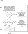
- the method 500 includes monitoring an output voltage (e.g., VOUT in FIGS. 2 and 3 , or VOUT 1 in FIG. 4 ) from a rectifier bridge and adaptive capacitive filter circuit faults at block 502 . If a fault is detected (determination block 504 ), a fault option for a switch arrangement (e.g., the switch arrangement 224 in FIGS.
- the method 500 determines if the output voltage is greater than a threshold (determination block 508 ). If the output voltage is greater than the threshold (determination block 508 ), a serial connection option for the switch arrangement is used at block 510 . If the output voltage is not greater than the threshold (determination block 508 ), a parallel connection option for the switch arrangement is used at block 512 . The method 500 may be repeated as needed.
- an adaptive capacitive filter circuit (e.g., adaptive capacitive filter circuit 210 in FIG. 2 , the adaptive capacitive filter circuit 210 A in FIG. 3 , or the adaptive capacitive filter circuit 210 B in FIG. 4 ) includes: a first adaptive capacitive filter circuit terminal (e.g., the first adaptive capacitive filter circuit terminals 212 in FIGS. 2 - 4 ) adapted to be coupled to a rectifier bridge output (e.g., the rectifier bridge output 206 in FIGS. 2 - 4 ); a second adaptive capacitive filter circuit terminal (e.g., the third rectifier bridge output terminal 216 in FIGS.
- a first adaptive capacitive filter circuit terminal e.g., the first adaptive capacitive filter circuit terminals 212 in FIGS. 2 - 4
- a rectifier bridge output e.g., the rectifier bridge output 206 in FIGS. 2 - 4
- a second adaptive capacitive filter circuit terminal e.g., the third rectifier bridge
- a first capacitor e.g., a first capacitor of set of capacitors 218 in FIGS. 2 and 4 , or C 3 in FIG. 3
- a second capacitor e.g., a second capacitor of set of capacitors 218 in FIGS. 2 and 4 , or C 4 in FIG. 3
- a first switch e.g., a first switch of the switch arrangement 224 in FIGS. 2 and 4 , or Q 2 in FIG.
- a second switch e.g., a first second of the switch arrangement 224 in FIGS. 2 and 4 , or Q 3 in FIG. 3
- a third switch e.g., a first third of the switch arrangement 224 in FIGS. 2 and 4 , or Q 4 in FIG. 3
- the adaptive capacitive filter circuit includes a control circuit (e.g., the control circuit 250 in FIGS. 2 and 4 , or the control circuit 250 A in FIG. 3 ) having a control circuit input (e.g., the control circuit input 252 in FIGS. 2 - 4 ) and a control circuit output (e.g., the control circuit output 254 in FIGS. 2 - 4 ), the control circuit input is adapted to be coupled to the first adaptive capacitive filter circuit terminal.
- the control circuit is configured to: receive an output voltage from the rectifier bridge output at the control circuit input; compare the output voltage with a threshold; and provide a control signal (e.g., CS 1 in FIGS.
- the adaptable capacitive filter circuit includes a fault sense circuit (e.g., the fault sense circuit 240 in FIGS. 2 and 4 , or the fault sense circuit 240 A in FIG. 3 ) having a fault sense circuit input (e.g., the fault sense circuit inputs 242 and 244 in FIG. 2 , or the fault sense circuit inputs 310 in FIG. 3 ) and a fault sense circuit output (e.g., the fault sense circuit output 246 in FIG. 2 ).
- the fault sense circuit input is configured to receive a sense signal.
- the fault sense circuit is configured to provide a second control signal (e.g., CS 2 in FIGS. 2 - 4 ) at the fault sense circuit output responsive to the sense signal.
- the second control signal indicates whether a fault condition exists for the adaptive capacitive filter circuit.
- the sense signal indicates a voltage across the first capacitor or the second capacitor
- the fault sense circuit is configured to: compare the voltage across the first capacitor or the second capacitor with a threshold; and provide the second control signal at the fault sense circuit output responsive to the comparison.
- the adaptive capacitive filter circuit includes control logic (e.g., the control logic 320 in FIGS. 3 and 4 ) having a first control logic input (e.g., the first control logic input 322 in FIG. 3 ), a second control logic input (e.g., the second control logic input 324 in FIG. 3 ), and control logic outputs (e.g., the first and second control logic outputs 326 and 328 in FIG. 3 ).
- the first control logic input is coupled to the control circuit output.
- the second control logic input is coupled to the fault sense circuit output.
- the control logic outputs are coupled to control terminals of the first switch, the second switch, and the third switch.
- the control logic of an adaptive capacitive filter circuit is configured to provide a set of switch drive signals at the control logic outputs responsive to the first control signal indicating the output voltage is greater than the threshold and the second control signal indicating absence of a fault condition.
- the set of switch drive signals includes a first switch drive signal to turn off the first switch, a second switch drive signal to turn off the second switch, and a third switch drive signal to turn on the third switch.
- the control logic is configured to provide a set of switch drive signals at the control logic outputs responsive to the first control signal indicating the output voltage is not greater than the threshold and the second control signal indicating absence of a fault condition.
- the set of switch drive signals includes a first switch drive signal to turn on the first switch, a second switch drive signal to turn on the second switch, and a third switch drive signal to turn off the third switch.
- the control logic is configured to provide a set of switch drive signals at the control logic outputs responsive to the second control signal indicating a fault condition exists.
- the set of switch drive signals including a first switch drive signal to turn on the first switch, a second switch drive signal to turn on the second switch, and a third switch drive signal to turn on the third switch.
- the adaptive capacitive filter circuit includes control circuitry configured to: operate the first switch, the second switch, and the third switch to couple the first capacitor and the second capacitor in series between the first adaptive capacitive filter circuit terminal and the second adaptive capacitive filter circuit terminal responsive to an output voltage of the rectifier bridge output being greater than a threshold; and operate the first switch, the second switch, and the third switch to couple the first capacitor and the second capacitor in parallel between the first adaptive capacitive filter circuit terminal and the second adaptive capacitive filter circuit terminal responsive to the output voltage of the rectifier bridge output not being greater than the threshold.
- control circuitry is configured to operate the first switch, the second switch, and the third switch to bypass the first capacitor and the second capacitor resulting in the first adaptive capacitive filter circuit terminal being coupled to ground responsive to a detected fault condition for the adaptive capacitive filter circuit.
- an integrated circuit (e.g., the integrated circuit 402 in FIG. 4 ) includes control circuitry (e.g., the control circuit 250 in FIGS. 2 and 4 , the control circuit 250 A in FIG. 3 , the fault sense circuit 240 in FIGS. 2 and 4 , the fault sense circuit 240 A in FIG. 3 , and the control logic 320 in FIGS. 3 and 4 ) for an adaptive capacitive filter circuit.
- the control circuitry is configured to: detect whether an output voltage (e.g., VOUT in FIGS. 2 and 3 , or VOUT 1 in FIG. 4 ) at a rectifier bridge output is greater than a threshold (e.g., VREF in FIG.
- control circuitry is further configured to: detect whether a fault condition exists for the adaptive capacitive filter circuit; and responsive to detecting a fault condition, provide a third set of switch drive signals for switches of the adaptive capacitive filter circuit to bypass the capacitors of the adaptive capacitive filter circuit.
- the switches of the adaptive capacitive filter circuit are part of the integrated circuit, and the capacitors of the adaptive capacitive filter circuit are external to the integrated circuit.
- the switches include a first switch (e.g., a first switch of the switch arrangement 224 in FIGS. 2 and 4 , or Q 2 in FIG. 3 ), a second switch (e.g., a second switch of the switch arrangement 224 in FIGS. 2 and 4 , or Q 3 in FIG. 3 ) and a third switch (e.g., a third switch of the switch arrangement 224 in FIGS. 2 and 4 , or Q 4 in FIG. 3 ),
- the capacitors include a first capacitor (e.g., a first capacitor of the set of capacitors 218 in FIGS. 2 and 4 , or C 3 in FIG.
- the integrated circuit includes: a first terminal (e.g., the first adaptive capacitive filter circuit terminal 212 in FIGS. 2 - 4 ) adapted to be coupled to the rectifier bridge output; a second terminal (e.g., the third adaptive capacitive filter circuit terminal 216 in FIGS. 2 - 4 ) adapted to be coupled to ground; a third terminal (e.g., the second terminal 332 in FIGS.
- the integrated circuit includes switching converter controller components configured to control power switches (e.g., the power switch 414 in FIG. 4 ) of a power stage (e.g., the power stage 410 in FIG.
- the switching converter controller components including a control loop (e.g., the control loop 406 in FIG. 4 ) and a driver circuit (e.g., the driver circuit 408 in FIG. 4 ).
- a system (e.g., the power management system 200 in FIG. 2 , the power management system 300 in FIG. 3 , or the system 400 in FIG. 4 ) includes an adaptive capacitive filter circuit having: a set of capacitors (e.g., the set of capacitors 218 FIGS. 2 and 4 , or C 3 and C 4 in FIG. 3 ); a first adaptive capacitive filter circuit terminal (e.g., the first adaptive capacitive filter circuit terminal 212 in FIGS. 2 - 4 ) adapted to be coupled to a rectifier bridge output (e.g., the rectifier bridge output 206 in FIGS.
- a set of capacitors e.g., the set of capacitors 218 FIGS. 2 and 4 , or C 3 and C 4 in FIG. 3
- a first adaptive capacitive filter circuit terminal e.g., the first adaptive capacitive filter circuit terminal 212 in FIGS. 2 - 4
- a rectifier bridge output e.g., the rectifier bridge output 206 in
- the adaptive capacitive filter circuit is configured to connect capacitors of the set of capacitors in series or in parallel between the first adaptive capacitive filter circuit terminal and the second adaptive capacitive filter circuit terminal responsive to a control signal (e.g., CS 1 in FIGS. 2 - 4 ).
- the adaptive capacitive filter circuit includes control circuitry (e.g., the control circuit 250 in FIGS. 2 and 4 , the control circuit 250 A in FIG. 3 , the fault sense circuit 240 in FIGS. 2 and 4 , the fault sense circuit 240 A in FIG. 3 , and the control logic 320 in FIGS. 3 and 4 ) and a switch arrangement (e.g., the switch arrangement 224 in FIGS. 2 and 4 , or Q 2 , Q 3 , and Q 4 in FIG. 3 ) controlled by the control circuitry.
- the control circuitry is configured to: provide the control signal responsive to a comparison of an output voltage (e.g., VOUT in FIGS. 2 and 3 , or VOUT 1 in FIG.
- a threshold e.g., VREF in FIG. 3
- a threshold e.g., VREF in FIG. 3
- responsive to the control signal indicating that the output voltage is greater than the threshold provide a first set of switch drive signals to the switch arrangement to couple capacitors of the set of capacitors in series; and responsive to the control signal indicating that the output voltage is not greater than the threshold, provide a second set of switch drive signals to the switch arrangement to couple the capacitors of the set of capacitors in parallel.
- control signal is a first control signal
- control circuitry is configured to: provide a second control signal (e.g., CS 2 in FIGS. 2 - 4 ) responsive to a comparison of a sense signal related to a capacitor of the set of capacitors with a threshold; and responsive to the second control signal indicating a fault condition, provide a third set of switch drive signals for switches of the adaptive capacitive filter circuit to bypass the capacitors of the adaptive capacitive filter circuit.
- a second control signal e.g., CS 2 in FIGS. 2 - 4
- the switch arrangement includes: a first switch (e.g., a first switch of the switch arrangement 224 in FIGS. 2 and 4 , or Q 2 in FIG. 3 ) coupled between a first capacitor (e.g., C 3 in FIG. 3 ) of the set of capacitors and ground; a second switch (e.g., a second switch of the switch arrangement 224 in FIGS. 2 and 4 , or Q 3 in FIG. 3 ) coupled between the first adaptive capacitive filter circuit terminal and a second capacitor (e.g., C 4 in FIG. 3 ) of the set of capacitors; and a third switch (e.g., a third switch of the switch arrangement 224 in FIGS. 2 and 4 , or Q 4 in FIG.
- a first switch e.g., a first switch of the switch arrangement 224 in FIGS. 2 and 4 , or Q 2 in FIG. 3
- a third switch e.g., a third switch of the switch arrangement 224 in FIGS. 2 and 4 , or Q
- the system includes: a power stage (e.g., the power stage 410 in FIG. 4 ) adapted to be coupled to the rectifier bridge output; and a switching converter controller (e.g., the control loop 406 and the driver circuit 408 in FIG. 4 ) coupled to the power stage and configured to provide power switch drive signals (e.g., HS_CS and LS_CS in FIG. 4 ) to the power stage, wherein the switching converter controller, the control circuitry, and the switch arrangement are part of an IC (e.g., the IC 402 in FIG. 4 ).
- a power stage e.g., the power stage 410 in FIG. 4
- a switching converter controller e.g., the control loop 406 and the driver circuit 408 in FIG. 4
- power switch drive signals e.g., HS_CS and LS_CS in FIG. 4
- the term “couple” may cover connections, communications, or signal paths that enable a functional relationship consistent with this description. For example, if device A generates a signal to control device B to perform an action: (a) in a first example, device A is coupled to device B by direct connection; or (b) in a second example, device A is coupled to device B through intervening component C if intervening component C does not alter the functional relationship between device A and device B, such that device B is controlled by device A via the control signal generated by device A.
- terminal As used herein, the terms “terminal,” “electrode,” “node,” “interconnection,” “pin,” “contact,” and “connection” are used interchangeably. Unless specifically stated to the contrary, these terms are generally used to mean an interconnection between or a terminus of a device element, a circuit element, an IC, a device or other electronics or semiconductor component.
- NFETs n-type metal-oxide semiconductor field-effect transistors
- PFETs p-type metal-oxide semiconductor field-effect transistors
- Other example embodiments may utilize NPN bipolar junction transistors (BJTs), PNP BJTs, or any other type of transistor. Accordingly, when referring to a current electrode, such electrode may be an emitter, collector, source or drain. Also, the control electrode may be a base or a gate.
- a device that is “configured to” perform a task or function may be configured (e.g., programmed and/or hardwired) at a time of manufacturing by a manufacturer to perform the function and/or may be configurable (or reconfigurable) by a user after manufacturing to perform the function and/or other additional or alternative functions.
- the configuring may be through firmware and/or software programming of the device, through a construction and/or layout of hardware components and interconnections of the device, or a combination thereof.
- a circuit or device that is described herein as including certain components may instead be adapted to be coupled to those components to form the described circuitry or device.
- a structure described as including one or more semiconductor elements such as transistors), one or more passive elements (such as resistors, capacitors, and/or inductors), and/or one or more sources (such as voltage and/or current sources) may instead include only the semiconductor elements within a single physical device (e.g., a semiconductor die and/or IC package) and may be adapted to be coupled to at least some of the passive elements and/or the sources to form the described structure either at a time of manufacture or after a time of manufacture, for example, by an end-user and/or a third-party.
- semiconductor elements such as transistors
- passive elements such as resistors, capacitors, and/or inductors
- sources such as voltage and/or current sources
- Circuits described herein are reconfigurable to include the replaced components to provide functionality at least partially similar to functionality available before the component replacement.
- Components shown as resistors are generally representative of any one or more elements coupled in series and/or parallel to provide an amount of impedance represented by the shown resistor.
- a resistor or capacitor shown and described herein as a single component may instead be multiple resistors or capacitors, respectively, coupled in parallel between the same nodes.
- a resistor or capacitor shown and described herein as a single component may instead be multiple resistors or capacitors, respectively, coupled in series between the same two nodes as the single resistor or capacitor.
- ground in this description include a chassis ground, an Earth ground, a floating ground, a virtual ground, a digital ground, a common ground, and/or any other form of ground connection applicable to, or suitable for, the teachings of this description. Unless otherwise stated, “about,” “approximately,” or “substantially” preceding a value means+/ ⁇ 10 percent of the stated value.
Landscapes
- Engineering & Computer Science (AREA)
- Power Engineering (AREA)
- Physics & Mathematics (AREA)
- Nonlinear Science (AREA)
- General Physics & Mathematics (AREA)
- Power Conversion In General (AREA)
- Networks Using Active Elements (AREA)
Abstract
Description
Claims (18)
Priority Applications (1)
| Application Number | Priority Date | Filing Date | Title |
|---|---|---|---|
| US17/573,579 US11817841B2 (en) | 2021-01-12 | 2022-01-11 | Adaptive capacitive filter circuit |
Applications Claiming Priority (2)
| Application Number | Priority Date | Filing Date | Title |
|---|---|---|---|
| US202163136267P | 2021-01-12 | 2021-01-12 | |
| US17/573,579 US11817841B2 (en) | 2021-01-12 | 2022-01-11 | Adaptive capacitive filter circuit |
Publications (2)
| Publication Number | Publication Date |
|---|---|
| US20220224314A1 US20220224314A1 (en) | 2022-07-14 |
| US11817841B2 true US11817841B2 (en) | 2023-11-14 |
Family
ID=82322337
Family Applications (1)
| Application Number | Title | Priority Date | Filing Date |
|---|---|---|---|
| US17/573,579 Active 2042-01-11 US11817841B2 (en) | 2021-01-12 | 2022-01-11 | Adaptive capacitive filter circuit |
Country Status (1)
| Country | Link |
|---|---|
| US (1) | US11817841B2 (en) |
Citations (6)
| Publication number | Priority date | Publication date | Assignee | Title |
|---|---|---|---|---|
| US9583174B1 (en) * | 2015-09-10 | 2017-02-28 | SK Hynix Inc. | Semiconductor devices and semiconductor systems |
| US20170294831A1 (en) * | 2016-04-11 | 2017-10-12 | Futurewei Technologies, Inc. | Method and Apparatus for Filtering a Rectified Voltage |
| US10033269B2 (en) * | 2016-04-29 | 2018-07-24 | Infineon Technologies Austria Ag | Voltage doubler with capacitor module for increasing capacitance |
| US20200136494A1 (en) * | 2018-10-30 | 2020-04-30 | Texas Instruments Incorporated | Dc-dc converter having a switch on-time control loop with a switched-capacitor circuit for error-based adjustment |
| US20210234471A1 (en) * | 2019-12-11 | 2021-07-29 | Gan Systems Inc. | Hybrid bulk capacitance circuit for ac input ac/dc switching mode power supplies |
| US20220311331A1 (en) * | 2021-03-29 | 2022-09-29 | Monolithic Power Systems, Inc. | Adaptive energy storage circuit |
-
2022
- 2022-01-11 US US17/573,579 patent/US11817841B2/en active Active
Patent Citations (6)
| Publication number | Priority date | Publication date | Assignee | Title |
|---|---|---|---|---|
| US9583174B1 (en) * | 2015-09-10 | 2017-02-28 | SK Hynix Inc. | Semiconductor devices and semiconductor systems |
| US20170294831A1 (en) * | 2016-04-11 | 2017-10-12 | Futurewei Technologies, Inc. | Method and Apparatus for Filtering a Rectified Voltage |
| US10033269B2 (en) * | 2016-04-29 | 2018-07-24 | Infineon Technologies Austria Ag | Voltage doubler with capacitor module for increasing capacitance |
| US20200136494A1 (en) * | 2018-10-30 | 2020-04-30 | Texas Instruments Incorporated | Dc-dc converter having a switch on-time control loop with a switched-capacitor circuit for error-based adjustment |
| US20210234471A1 (en) * | 2019-12-11 | 2021-07-29 | Gan Systems Inc. | Hybrid bulk capacitance circuit for ac input ac/dc switching mode power supplies |
| US20220311331A1 (en) * | 2021-03-29 | 2022-09-29 | Monolithic Power Systems, Inc. | Adaptive energy storage circuit |
Also Published As
| Publication number | Publication date |
|---|---|
| US20220224314A1 (en) | 2022-07-14 |
Similar Documents
| Publication | Publication Date | Title |
|---|---|---|
| US10033281B2 (en) | Integrated circuit with configurable control and power switches | |
| KR102416267B1 (en) | Protection of switched capacitor power converter | |
| US9679885B2 (en) | Integrated protection devices with monitoring of electrical characteristics | |
| CN101189795A (en) | Power Controllers and Semiconductor Devices | |
| JP2016163533A (en) | Isolated dc/dc converter and feedback circuit for the same, power supply device, power supply adapter, and electronic apparatus using the same | |
| CN111327024A (en) | Protection circuit with disconnect switch for power system | |
| US20110110121A1 (en) | Power supply circuit | |
| US20250293602A1 (en) | Peak current limit management for high frequency buck converter | |
| US20250116728A1 (en) | Open fault detection for power converters | |
| EP4635083A1 (en) | Driver discharge circuit | |
| KR102033548B1 (en) | Apparatus and method for protection of bi-directional dc-dc converter | |
| US11114941B2 (en) | Reduced voltage ratings for power transistors in a buck converter | |
| US20250330095A1 (en) | Dc-dc converter and power supply semiconductor integrated circuit | |
| JPH11149320A (en) | Power circuit protection measures | |
| US11817841B2 (en) | Adaptive capacitive filter circuit | |
| US20250192545A1 (en) | Short detection circuit | |
| US20220329168A1 (en) | Self-powered solid state relay using digital isolators | |
| US12301102B2 (en) | Power factor correction | |
| US12261429B2 (en) | Short detection circuit | |
| US20250181090A1 (en) | Supply-dependent threshold for over-curent protection | |
| US12401272B2 (en) | Totem pole power factor correction circuit | |
| US20240364337A1 (en) | Excessive current protection for bootstrap capacitor charging | |
| US20250273948A1 (en) | Methods and apparatus to disconnect circuitry responsive to a fault condition | |
| KR102877538B1 (en) | Power apparatus and control method thereof | |
| US20250088093A1 (en) | Circuit with output terminal and selective clamping |
Legal Events
| Date | Code | Title | Description |
|---|---|---|---|
| FEPP | Fee payment procedure |
Free format text: ENTITY STATUS SET TO UNDISCOUNTED (ORIGINAL EVENT CODE: BIG.); ENTITY STATUS OF PATENT OWNER: LARGE ENTITY |
|
| STPP | Information on status: patent application and granting procedure in general |
Free format text: SENT TO CLASSIFICATION CONTRACTOR |
|
| STPP | Information on status: patent application and granting procedure in general |
Free format text: DOCKETED NEW CASE - READY FOR EXAMINATION |
|
| AS | Assignment |
Owner name: TEXAS INSTRUMENTS INCORPORATED, TEXAS Free format text: ASSIGNMENT OF ASSIGNORS INTEREST;ASSIGNOR:COHEN, ISAAC;REEL/FRAME:061887/0578 Effective date: 20221126 |
|
| STPP | Information on status: patent application and granting procedure in general |
Free format text: NON FINAL ACTION MAILED |
|
| STPP | Information on status: patent application and granting procedure in general |
Free format text: NOTICE OF ALLOWANCE MAILED -- APPLICATION RECEIVED IN OFFICE OF PUBLICATIONS |
|
| STPP | Information on status: patent application and granting procedure in general |
Free format text: PUBLICATIONS -- ISSUE FEE PAYMENT VERIFIED Free format text: AWAITING TC RESP, ISSUE FEE PAYMENT VERIFIED |
|
| STCF | Information on status: patent grant |
Free format text: PATENTED CASE |