US11796747B2 - Diffractive optical waveguide and display device - Google Patents
Diffractive optical waveguide and display device Download PDFInfo
- Publication number
- US11796747B2 US11796747B2 US18/153,515 US202318153515A US11796747B2 US 11796747 B2 US11796747 B2 US 11796747B2 US 202318153515 A US202318153515 A US 202318153515A US 11796747 B2 US11796747 B2 US 11796747B2
- Authority
- US
- United States
- Prior art keywords
- grating
- coupling
- light
- return
- diffractive optical
- Prior art date
- Legal status (The legal status is an assumption and is not a legal conclusion. Google has not performed a legal analysis and makes no representation as to the accuracy of the status listed.)
- Active
Links
- 230000003287 optical effect Effects 0.000 title claims abstract description 142
- 239000000758 substrate Substances 0.000 claims abstract description 108
- 230000001902 propagating effect Effects 0.000 claims abstract description 17
- 239000013598 vector Substances 0.000 claims description 92
- 238000010168 coupling process Methods 0.000 abstract description 12
- 238000005859 coupling reaction Methods 0.000 abstract description 12
- 230000008878 coupling Effects 0.000 abstract description 11
- 238000010586 diagram Methods 0.000 description 16
- 230000003190 augmentative effect Effects 0.000 description 5
- 230000000694 effects Effects 0.000 description 3
- 238000005516 engineering process Methods 0.000 description 3
- 230000006872 improvement Effects 0.000 description 3
- 239000013589 supplement Substances 0.000 description 3
- 230000009286 beneficial effect Effects 0.000 description 2
- 238000004364 calculation method Methods 0.000 description 2
- 230000007812 deficiency Effects 0.000 description 2
- 238000001514 detection method Methods 0.000 description 2
- 210000001747 pupil Anatomy 0.000 description 2
- 241000282412 Homo Species 0.000 description 1
- 241000282414 Homo sapiens Species 0.000 description 1
- 239000011521 glass Substances 0.000 description 1
- 230000003993 interaction Effects 0.000 description 1
- 238000004519 manufacturing process Methods 0.000 description 1
- 230000007246 mechanism Effects 0.000 description 1
- 238000000034 method Methods 0.000 description 1
- 230000000737 periodic effect Effects 0.000 description 1
- 230000008569 process Effects 0.000 description 1
- 239000004065 semiconductor Substances 0.000 description 1
- 238000004088 simulation Methods 0.000 description 1
Images


Classifications
-
- G—PHYSICS
- G02—OPTICS
- G02B—OPTICAL ELEMENTS, SYSTEMS OR APPARATUS
- G02B27/00—Optical systems or apparatus not provided for by any of the groups G02B1/00 - G02B26/00, G02B30/00
- G02B27/01—Head-up displays
- G02B27/017—Head mounted
- G02B27/0172—Head mounted characterised by optical features
-
- G—PHYSICS
- G02—OPTICS
- G02B—OPTICAL ELEMENTS, SYSTEMS OR APPARATUS
- G02B6/00—Light guides; Structural details of arrangements comprising light guides and other optical elements, e.g. couplings
- G02B6/10—Light guides; Structural details of arrangements comprising light guides and other optical elements, e.g. couplings of the optical waveguide type
-
- G—PHYSICS
- G02—OPTICS
- G02B—OPTICAL ELEMENTS, SYSTEMS OR APPARATUS
- G02B6/00—Light guides; Structural details of arrangements comprising light guides and other optical elements, e.g. couplings
- G02B6/24—Coupling light guides
- G02B6/42—Coupling light guides with opto-electronic elements
- G02B6/4201—Packages, e.g. shape, construction, internal or external details
- G02B6/4204—Packages, e.g. shape, construction, internal or external details the coupling comprising intermediate optical elements, e.g. lenses, holograms
-
- G—PHYSICS
- G02—OPTICS
- G02B—OPTICAL ELEMENTS, SYSTEMS OR APPARATUS
- G02B27/00—Optical systems or apparatus not provided for by any of the groups G02B1/00 - G02B26/00, G02B30/00
- G02B27/0081—Optical systems or apparatus not provided for by any of the groups G02B1/00 - G02B26/00, G02B30/00 with means for altering, e.g. enlarging, the entrance or exit pupil
-
- G—PHYSICS
- G02—OPTICS
- G02B—OPTICAL ELEMENTS, SYSTEMS OR APPARATUS
- G02B27/00—Optical systems or apparatus not provided for by any of the groups G02B1/00 - G02B26/00, G02B30/00
- G02B27/42—Diffraction optics, i.e. systems including a diffractive element being designed for providing a diffractive effect
- G02B27/4205—Diffraction optics, i.e. systems including a diffractive element being designed for providing a diffractive effect having a diffractive optical element [DOE] contributing to image formation, e.g. whereby modulation transfer function MTF or optical aberrations are relevant
-
- G—PHYSICS
- G02—OPTICS
- G02B—OPTICAL ELEMENTS, SYSTEMS OR APPARATUS
- G02B27/00—Optical systems or apparatus not provided for by any of the groups G02B1/00 - G02B26/00, G02B30/00
- G02B27/42—Diffraction optics, i.e. systems including a diffractive element being designed for providing a diffractive effect
- G02B27/4272—Diffraction optics, i.e. systems including a diffractive element being designed for providing a diffractive effect having plural diffractive elements positioned sequentially along the optical path
-
- G—PHYSICS
- G02—OPTICS
- G02B—OPTICAL ELEMENTS, SYSTEMS OR APPARATUS
- G02B5/00—Optical elements other than lenses
- G02B5/18—Diffraction gratings
- G02B5/1814—Diffraction gratings structurally combined with one or more further optical elements, e.g. lenses, mirrors, prisms or other diffraction gratings
- G02B5/1819—Plural gratings positioned on the same surface, e.g. array of gratings
-
- G—PHYSICS
- G02—OPTICS
- G02B—OPTICAL ELEMENTS, SYSTEMS OR APPARATUS
- G02B27/00—Optical systems or apparatus not provided for by any of the groups G02B1/00 - G02B26/00, G02B30/00
- G02B27/01—Head-up displays
- G02B27/017—Head mounted
- G02B2027/0178—Eyeglass type
Definitions
- the invention relates to display technology based on diffraction, in particular to a diffractive optical waveguide and a display device comprising the same, which can be used for augmented reality display.
- Augmented Reality (AR) display can provide human beings with more dimensional information, and has attracted widespread attention.
- AR glasses are one of the important mediums in the field of augmented reality display.
- Diffractive optical waveguide has the advantages of strong mass production, thinness, etc. It has gradually been recognized in the field of AR display and is expected to become the mainstream technology development direction in the field of AR in the future.
- the coupling-in grating a couples incident light carrying image information into the waveguide substrate.
- the coupling-out grating b expands the light carrying image information in a plane where the waveguide substrate is located, and at the same time couples the light out of the waveguide substrate.
- the light-return grating c is arranged around the end of the coupling-out grating b away from the coupling-in grating a, and is used to return the light that leaves the coupling-out grating b and continues to propagate in the waveguide substrate to the coupling-out grating b.
- the improvement of the overall optical coupling efficiency of the diffractive optical waveguide by the design shown in FIG. 13 is still very limited.
- the optical output field of the coupling-out grating b tends to be in a non-uniform state where the central area (as shown by the dotted line box in FIG. 13 ) is dark and the surrounding area is bright, resulting in a poor display effect.
- the invention aims to provide a diffractive optical waveguide and a display device comprising the diffractive optical waveguide, so as to at least partly address the deficiencies in the prior art.
- a diffractive optical waveguide comprising a waveguide substrate, the waveguide substrate being formed with a coupling-in grating and a coupling-out grating, the coupling-in grating being configured to couple an input beam into the waveguide substrate so that the input beam propagates in the waveguide substrate through total reflection and forms a first beam of light propagating toward the coupling-out grating and a second beam of light not propagating toward the coupling-out grating, and the coupling-out grating being configured to couple at least a part of the light propagating therein out of the waveguide substrate by diffraction, wherein the waveguide substrate is further formed with a coupling-in end light-return grating, and the coupling-in end light-return grating is configured to diffract the second beam of light, so as to make it propagate towards the coupling-out grating.
- the coupling-in end light-return grating is configured to diffract the second beam of light to form a third beam of light, and the third beam of light propagates in the waveguide substrate at the same total reflection angle as that of the first beam of light.
- the coupling-in grating has a grating period d 1 along a direction
- the coupling-in grating and the coupling-in end light-return grating are respectively formed on two opposite surfaces of the waveguide substrate, and in a projection perpendicular to the two surfaces, the coupling-in end light-return grating partially overlaps the coupling-in grating.
- the coupling-in grating has a first grating vector
- the coupling-in end light-return grating is a one-dimensional grating
- the coupling-in end light-return grating has a grating vector which is parallel to the first grating vector.
- the coupling-in end light-return grating has a trapezoidal shape, two parallel sides of the trapezoidal shape are perpendicular to the first grating vector, and the width of the coupling-in end light-return grating increases along a propagation direction of the second beam of light.
- the coupling-in grating is a two-dimensional grating.
- the coupling-in grating is a one-dimensional grating and has a first grating vector
- the coupling-in end light-return grating is a one-dimensional grating
- the coupling-in end light-return grating has a grating vector which is at a predetermined angle with respect to the first grating vector.
- the coupling-in grating has a first grating vector
- the coupling-in end light-return grating comprises a first one-dimensional grating and a second one-dimensional grating
- the first one-dimensional grating has a grating vector which forms a first angle with respect to the first grating vector
- the second one-dimensional grating has a grating vector which forms a second angle with respect to the first grating vector.
- the first angle and the second angle are angles with opposite directions and are both 60°.
- the waveguide substrate is further formed with a deflection grating, and the deflection grating is configured to deflect the light from the coupling-in end light-return grating toward the coupling-out grating.
- the width of the coupling-in end light-return grating in the direction perpendicular to the first grating vector is greater than or equal to the width of the coupling-in grating in the direction.
- the waveguide substrate is further formed with a coupling-out end light-return grating, and the coupling-out end light-return grating is configured to receive light from the coupling-out grating and diffract the light back to the coupling-out grating; and the coupling-out grating and the coupling-out end light-return grating are respectively formed on two opposite surfaces of the waveguide substrate, and in a projection perpendicular to the two surfaces, the coupling-out end light-return grating partially overlaps the coupling-out grating.
- the coupling-out grating has a first side for receiving light from the coupling-in grating, a second side opposite to the first side and a third side and a fourth side between the first side and the second side, and in the projection, the coupling-out end light-return grating lies across the second side.
- the coupling-out end light-return grating lies across the second side, the third side, and the fourth side.
- the coupling-out end light-return grating is formed in a U shape.
- the coupling-out end light-return grating comprises a grating region formed with a grating structure and several grating-free regions distributed in the grating region.
- the coupling-in grating is a one-dimensional grating
- the waveguide substrate is further formed with a turning grating, and the light from the coupling-in grating is expanded in one dimension and deflected by the turning grating so as to propagate toward the coupling-out grating
- the waveguide substrate is also formed with an intermediate light-return grating which is configured to receive light from the turning grating and diffract it back to the turning grating
- the turning grating and the intermediate light-return grating are respectively formed on the two surfaces of the waveguide substrate, and in the projection, the intermediate light-return grating partially overlaps the turning grating.
- the turning grating has a first edge opposite to the coupling-in grating and a second edge opposite to the coupling-out grating, and in the projection, the intermediate light-return grating lies across the first edge and the second edge.
- a display device comprising the diffractive optical waveguide.
- the display device is a near-eye display device and comprises a lens and a frame for keeping the lens close to the eye, the lens comprising the diffractive optical waveguide.
- the frame comprises a holder abutting against the lens to hold the lens, and the coupling-in end light-return grating of the diffractive optical waveguide is located in an area where the lens abuts the holder.
- the display device further comprises an optical machine for projecting light with image information onto the coupling-in grating of the diffractive optical waveguide, the optical machine is mounted on the holder and faces the coupling-in grating.
- the display device is an augmented reality display device or a virtual reality display device.
- the optical coupling efficiency of the diffractive optical waveguide is improved, and the optical energy distribution uniformity of the optical output field of the diffractive optical waveguide is advantageously improved.
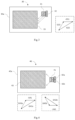
- FIG. 1 is a schematic diagram of Example 1 of a diffractive optical waveguide according to Embodiment 1 of the invention.
- FIG. 2 is a schematic diagram of Example 2 of a diffractive optical waveguide according to Embodiment 1 of the invention.
- FIG. 3 is a schematic diagram of Example 1 of a diffractive optical waveguide according to Embodiment 2 of the invention.
- FIG. 4 is a schematic diagram of Example 2 of a diffractive optical waveguide according to Embodiment 2 of the invention.
- FIG. 5 is a schematic diagram of Example 3 of a diffractive optical waveguide according to Embodiment 2 of the invention.
- FIG. 6 is a schematic diagram of Example 1 of a diffractive optical waveguide according to Embodiment 3 of the invention.
- FIG. 7 is a schematic diagram of Example 2 of a diffractive optical waveguide according to Embodiment 3 of the invention.
- FIG. 8 is a schematic diagram of Example 1 of a diffractive optical waveguide according to Embodiment 4 of the invention.
- FIG. 9 is a schematic diagram of Example 2 of a diffractive optical waveguide according to Embodiment 4 of the invention.
- FIG. 10 is a schematic diagram of an example of a diffractive optical waveguide according to Embodiment 5 of the invention.
- FIG. 11 is a schematic diagram of an example of a display device according to an embodiment of the invention.
- FIG. 12 is a schematic diagram of lens/diffractive optical waveguide used in the display device shown in FIG. 11 ;
- FIG. 13 is a schematic diagram of a diffractive optical waveguide for display in the prior art.
- Embodiment 1 of the invention a diffractive optical waveguide according to Embodiment 1 of the invention will be introduced with reference to FIG. 1 and FIG. 2 .
- FIG. 1 shows Example 1 of the diffractive optical waveguide according to Embodiment 1, that is, diffractive optical waveguide 10 .
- the diffractive optical waveguide 10 comprises a waveguide substrate 10 a , and the waveguide substrate 10 a is formed with a coupling-in grating 11 , a coupling-in end light-return grating 12 , and a coupling-out grating 13 .
- the coupling-in grating 11 is a one-dimensional grating, which is configured to couple an input beam irradiated on the coupling-in grating 11 into the waveguide substrate 10 a so that it propagates in the waveguide substrate 10 a through total reflection and forms a first beam of light propagating toward the coupling-out grating 13 (for example, as shown by a leftward arrow in FIG. 1 ) and a second beam of light not propagating toward the coupling-out grating 13 (for example, as shown by a rightward arrow in FIG. 1 ).
- the coupling-in end light-return grating 12 is configured to diffract the second beam of light, so as to make it propagate towards the coupling-out grating 13 .
- the coupling-out grating 13 is a two-dimensional grating configured to couple at least a part of the light propagating therein out of the waveguide substrate 10 a by diffraction.
- the coupling-in grating 11 has a plurality of linear grooves periodically arranged along the direction indicated by the arrow in FIG. 1 (see the figure in the lower left corner of FIG. 1 ). That is, the extension direction of the linear grooves of the coupling-in grating 11 is perpendicular to the direction shown by the arrow.
- the input beam (such as light carrying image information) irradiated on the coupling-in grating 11 from the outside of the waveguide substrate 10 a is diffracted by the coupling-in grating 11 to form positive first-order diffracted light and negative first-order diffracted light.
- the positive first-order diffracted light propagates in the waveguide substrate 10 a through total reflection (total internal reflection) along the leftward arrow in FIG. 1 to form the first beam of light;
- the negative first-order diffracted light propagates in the waveguide substrate 10 a through total reflection along the rightward arrow in FIG. 1 to form the second beam of light.
- the coupling-in grating 11 has a grating vector G 11 as shown in the figure in the lower left corner of FIG. 1 .
- “grating vector” is used to describe the periodic characteristics of the grating structure, wherein the direction of the “grating vector” is parallel to the direction along which the structure of the grating is periodically changed/arranged (for example, perpendicular to the grating lines/grooves direction) and is consistent with the propagation direction of the positive first-order diffracted light of the grating; the magnitude of the “grating vector” is 2 ⁇ /d, where d is the period of the grating structure in the direction of the “grating vector”, also known as “grating period”.
- the coupling-in end light-return grating 12 is arranged on the opposite side of the coupling-in grating 11 to the coupling-out grating 13 .
- the coupling-in end light-return grating 12 is configured to diffract the second beam of light to form a third beam of light.
- the third beam of light propagates along the same direction as the first beam of light (for example, along the leftward arrow in FIG. 1 ), so as to enter the coupling-out grating 13 .
- the coupling-in end light-return grating 12 is configured so that the third beam of light propagates in the waveguide substrate at the same total reflection angle as the first beam of light.
- the coupling-in end light-return grating 12 can have a grating vector G 12 as shown in the figure in the lower right corner of FIG. 1 , the grating vector G 12 has a direction that is the same as the direction of G 11 , and a magnitude that is twice of that of the grating vector G 11 .
- Light diffracted by grating has complicated angle changes, which is difficult to introduce here concisely and clearly.
- the negative first-order diffracted light (the second beam of light) of the coupling-in grating 11 is equivalent to that obtained by applying the influence of a grating vector ⁇ G 11 opposite to the direction of the grating vector G 11 on the input beam;
- the second beam of light diffracted by the coupling-in end light-return grating 12 is equivalent to superimposing the influence of the coupling-in end light-return grating 12 on the influence of the grating vector ⁇ G 11 , such that the third beam of light is obtained.
- the negative first-order diffracted light (the second beam of light) of the coupling-in grating 11 is equivalent to that obtained by applying the influence of a grating vector ⁇ G 11 opposite to the direction of the grating vector G 11 on the input beam
- the second beam of light diffracted by the coupling-in end light-return grating 12 is equivalent to superimposing the influence of the coupling-in end light-return grating 12 on the influence of the grating
- the overall effect of the grating vectors ⁇ G 11 and G 12 on the third beam of light is equivalent to the influence of the grating vector G 11 on the input beam, which is the same as the first beam of light. This is consistent with the result of calculating the light angle based on the refraction, diffraction, and reflection of the input beam incident on the diffractive optical waveguide 10 .
- the coupling-in end light-return grating 12 has a trapezoidal shape, and two sides parallel to each other of the trapezoidal shape are perpendicular to the first grating vector G 11 of the coupling-in grating 11 ; the width of the coupling-in end light-return grating 12 increases along the propagation direction of the second beam of light.
- the received input beam is not completely perpendicular to the surface of the waveguide substrate 10 a , but has a certain field of view (FOV), which results in that each of the first beam of light and the second beam of light obtained through the diffraction of the coupling-in grating 11 propagates through total reflection in the waveguide substrate 10 a with a certain expanding angle with respect to the direction shown by the arrow in FIG. 1 .
- the coupling-in end light-return grating 12 preferably has the trapezoidal shape.
- the coupling-in end light-return grating 12 can also have any other suitable shape whose width in the direction perpendicular to the grating vector G 11 of the coupling-in grating is greater than or equal to the width of the coupling-in grating 11 . This is applicable to any coupling-in end light-return grating in diffractive optical waveguides of each embodiment described below, and will not be repeated in the following.
- FIG. 2 shows Example 2 of the diffractive optical waveguide according to Embodiment 1, that is, diffractive optical waveguide 20 .
- the diffractive optical waveguide 20 comprises a waveguide substrate 20 a , and the waveguide substrate 20 a is formed with a coupling-in grating 21 , a coupling-in end light-return grating 22 , a coupling-out grating 23 and a turning grating 25 .
- the coupling-in grating 21 is a one-dimensional grating, which has a grating vector G 21 as shown in the lower left corner of FIG. 2 .
- the coupling-in end light-return grating 22 has a grating vector G 22 , and the direction of the grating vector G 22 is the same as that of the grating vector G 21 , and its magnitude is twice of that of the latter.
- the coupling-in grating 21 and the coupling-in end light-return grating 22 can have the same structure and function as the coupling-in grating 11 and the coupling-in end light-return grating 12 in the diffractive optical waveguide 10 introduced above with reference to FIG. 1 , and will not be repeated here.
- the coupling-in end light-return grating 22 can have a rectangular shape with a width greater than the coupling-in grating 21 in the direction perpendicular to the grating vector G 21 .
- the coupling-out grating 23 and the turning grating 25 are one-dimensional gratings, and the light from the coupling-in grating 21 propagates towards the coupling-out grating 23 after deflection and one-dimensional expansion of the turning grating 25 in one direction (such as the left and right directions in FIG. 2 ).
- the coupling-out grating 23 expands the received light in another direction (such as the up and down directions in FIG. 2 ) and gradually couples the light out of the waveguide substrate 20 a during the expansion process. In applications for image display, this can provide image display after two-dimensional pupil expansion.
- the refractive index of the waveguide substrate is 1.816
- the coupling-in end light-return grating is a rectangular grating with a grating period of 210 nm, a duty cycle of 26%, and a depth of 210 nm;
- the wavelength of the input beam is 532 nm, and the angle of the input beam (FOV) changes within the range of ⁇ 15° ⁇ 15° in the plane perpendicular to the x-axis shown in FIG. 2 and remains in the plane perpendicular to the y-axis as 0°; and
- the detection surface D of the photodetector is configured to receive at least part of the light coupled out from the coupling-in grating 23 .
- the optical energy detected by the photodetector with or without the coupling-in end light-return grating 22 is calculated respectively with a certain input beam angle, and the following results are obtained:
- the optical energy of the input beam is fixed.
- the coupling-in end light-return grating helps to improve the optical coupling efficiency of the diffractive optical waveguide, and corresponding to a certain range of field of view, it can greatly improve the optical coupling efficiency. This advantageously improves the brightness of image displays based on diffractive optical waveguide.
- both the coupling-in gratings 11 and 21 are one-dimensional gratings. It should be understood that the invention is not limited to this, and in other embodiments, a two-dimensional grating can also be used as the coupling-in grating.
- the coupling-in grating has more than one grating vector, and the grating vector of the coupling-in end light-return grating can be in the same/parallel direction as one of the grating vectors of the coupling-in grating, as long as the diffraction through the coupling-in end light-return grating can make the second beam of light from the coupling-in grating propagate toward the coupling-out grating.
- FIGS. 3 to 5 show different examples of diffractive optical waveguide according to Embodiment 2 of the invention, wherein a direction of a grating vector of coupling-in end light-return grating is at a predetermined angle with respect to a direction of a grating vector of a coupling-in grating.
- a diffractive optical waveguide 30 comprises a waveguide substrate 30 a and a coupling-in grating 31 , a coupling-in end light-return grating 32 , and a coupling-out grating 33 formed on the waveguide substrate 30 a .
- the coupling-in grating 31 is a one-dimensional grating and has a grating vector G 31 (the figure on the right of FIG. 3 shows a grating vector ⁇ G 31 which is opposite to the grating vector G 31 and has the same magnitude).
- the coupling-in end light-return grating 32 is a one-dimensional grating and has a grating vector G 32 . As shown in FIG. 3 , the direction of the grating vector G 32 is at an angle to the direction of the grating vector G 31 .
- the coupling-out grating 33 is a two-dimensional grating, and one of the grating vectors of the two-dimensional grating is G 33 .
- the coupling-in end light-return grating 32 is configured so that the vector sum of the grating vector G 32 , the grating vector ⁇ G 31 and the grating vector G 33 is zero.
- the input beam is diffracted by the coupling-in grating 31 to form positive first-order diffracted light (a first beam of light) propagating toward the coupling-out grating 33 and negative first-order diffracted light (a second beam of light) not propagating toward the coupling-out grating 33 ;
- the second beam of light passes through the diffraction of the coupling-in end light-return grating 32 , propagates toward the coupling-out grating 33 , and finally couples out from the waveguide substrate 30 a through the diffraction of the coupling-out grating 33 , and the light coupled out from the waveguide substrate 30 a remains the same angle as the input beam, so that the image information carried by the input beam can be restored.
- the coupling-in end light-return grating 32 can be arranged so that the light follows, for example, the direction shown by the parallel arrow in the figure on the right of FIG. 3 to propagate toward the coupling-out grating 33 to supplement the insufficient brightness of the lower half of the coupling-out grating 33 caused by the upward bias of the coupling-in grating 31 .
- the diffractive optical waveguide 40 comprises a waveguide substrate 40 a and a coupling-in grating 41 , a coupling-in end light-return grating 42 , and a coupling-out grating 43 formed on the waveguide substrate 40 a .
- the coupling-in grating 41 is a one-dimensional grating and has a grating vector G 41 (the figure on the right of FIG. 4 shows a grating vector ⁇ G 41 which is opposite to the grating vector G 41 and has the same magnitude).
- the coupling-in end light-return grating 42 comprises a first one-dimensional grating 42 a and a second one-dimensional grating 42 b , a grating vector G 42 a of the first one-dimensional grating 42 a forms a first angle with respect to the grating vector G 41 and a grating vector G 42 b of the second one-dimensional grating 42 b forms a second angle with respect to the grating vector G 41 .
- a grating vector G 42 a of the first one-dimensional grating 42 a forms a first angle with respect to the grating vector G 41
- a grating vector G 42 b of the second one-dimensional grating 42 b forms a second angle with respect to the grating vector G 41 .
- the light diffracted by the first one-dimensional grating 42 a and the second one-dimensional grating 42 b converges toward the coupling-out grating 43 ;
- the diffracted light can also diverge toward the coupling-out grating 43 .
- the first angle and the second angle are in opposite directions, and both are 60°.
- the coupling-out grating 43 is a two-dimensional grating, and the two grating vectors of the two-dimensional grating are G 43 a and G 43 b .
- the coupling-in end light-return grating 42 is configured so that the vector sum of the grating vector G 42 a , the grating vector ⁇ G 41 , and the grating vector G 43 a is zero (as shown in the figure in the lower left corner of FIG. 4 ), and the vector sum of the grating vector G 42 b , the grating vector ⁇ G 41 and the grating vector G 43 b is zero (as shown in the figure in the lower right corner of FIG. 4 ).
- negative first-order diffracted light (a second beam of light) formed by the input beam through the diffraction of the coupling-in grating 41 is coupled out from the waveguide substrate 40 a through the diffraction of the coupling-in end light-return grating 42 and the coupling-out grating 43 , and the light coupled out from the waveguide substrate 40 a maintains the same angle as the input beam, so that the image information carried by the input beam can be restored.
- the design of the diffractive optical waveguide 40 helps to supplement the insufficient light intensity at the two corners of the coupling-out grating 43 near the coupling-in grating 41 , thereby improving the uniformity of the optical output field of the diffractive optical waveguide.
- the diffractive optical waveguide 50 comprises a waveguide substrate 50 a and a coupling-in grating 51 , a coupling-in end light-return grating 52 , and a coupling-out grating 53 formed on the waveguide substrate 50 a .
- the coupling-in grating 51 is a one-dimensional grating and has a grating vector G 51 (the figure on the right of FIG. 5 shows a grating vector ⁇ G 51 which is opposite to the grating vector G 51 and has the same magnitude).
- the coupling-in end light-return grating 52 comprises a first one-dimensional grating 52 a and a second one-dimensional grating 52 b , a grating vector G 52 a of the first one-dimensional grating 52 a forms a first angle with respect to the grating vector G 51 and a grating vector G 52 b of the second one-dimensional grating 52 b forms a second angle with respect to the grating vector G 51 .
- a grating vector G 52 a of the first one-dimensional grating 52 a forms a first angle with respect to the grating vector G 51
- a grating vector G 52 b of the second one-dimensional grating 52 b forms a second angle with respect to the grating vector G 51 .
- a deflection grating 57 is formed on the waveguide substrate 50 a , comprising a grating 57 a and a grating 57 b , which is configured to deflect light from the coupling-in end light-return grating toward the coupling-out grating 53 .
- the first angle and the second angle are in opposite directions, and both are 60°.
- the coupling-out grating 53 is a two-dimensional grating, and two grating vectors of the two-dimensional grating are G 53 a and G 53 b .
- the deflection gratings 57 a and 57 b have grating vectors G 57 a and G 57 b respectively.
- the coupling-in end light-return grating and the deflection grating are configured so that the vector sum of the grating vector G 52 a , the grating vector ⁇ G 51 , the grating vector 57 a , and the grating vector G 53 a is zero (as shown in the figure in the lower left corner of FIG.
- the vector sum of the grating vector G 52 b , the grating vector ⁇ G 51 , the grating vector 57 b and the grating vector G 53 b is zero (as shown in the figure in the lower right corner of FIG. 5 ).
- negative first-order diffracted light (a second beam of light) formed by the input beam through the diffraction of the coupling-in grating 51 is coupled out from the waveguide substrate 50 a through the diffraction of the coupling-in end light-return grating 52 , the deflection grating 57 , and the coupling-out grating 53 , and the light coupled out from the waveguide substrate 50 a maintains the same angle as the input beam so that the image information carried by the input beam can be restored.
- the design of the diffraction waveguide 50 helps to supplement the insufficient light intensity at the two corners of the coupling-out grating 53 near the coupling-in grating 51 , thereby improving the uniformity of the optical output field of the diffractive optical waveguide.
- the arrangement of the deflection gratings 57 a and 57 b helps to make the light from the coupling-in end light-return grating 52 propagate a longer distance in the coupling-out grating 53 , thereby being coupled out more fully by the out-coupling grating 53 to the outside of the waveguide substrate 60 a , thereby improving the optical coupling efficiency.
- a deflection grating can also be provided near the lower right corner of the coupling-out grating 33 .
- FIGS. 6 and 7 show different examples of diffractive optical waveguide according to Embodiment 3 of the invention, wherein a coupling-in grating and a coupling-in end light-return grating are respectively formed on two opposite surfaces of the waveguide substrate.
- a diffractive optical waveguide 60 according to Embodiment 3 of the invention shown in FIG. 6 comprises a waveguide substrate 60 a and a coupling-in grating 61 , a coupling-in end light-return grating 62 , and a coupling-out grating 63 formed on the waveguide substrate 60 a .
- the coupling-in grating 61 , the coupling-in end light-return grating 62 , and the coupling-out grating 63 of the diffractive optical waveguide 60 have the same configuration as the coupling-in grating 11 , the coupling-in end light-return grating 12 and the coupling-out grating 13 of the diffractive optical waveguide 10 shown in FIG.
- the coupling-in grating 61 and the coupling-in end light-return grating 62 are respectively formed on two opposite surfaces A and B of the waveguide substrate 60 a .
- the coupling-in grating 61 and the coupling-out grating 63 are formed on the surface A of the waveguide substrate 60 a
- the coupling-in end light-return grating 62 is formed on the surface B of the waveguide substrate 60 a .
- the coupling-out grating 63 and the coupling-in end light-return grating 62 can also be formed on the same surface.
- a diffractive optical waveguide 70 according to Embodiment 3 of the invention comprises a waveguide substrate 70 a and a coupling-in grating 71 , a coupling-in end light-return grating 72 , a coupling-out grating 73 and a turning grating 75 formed on the waveguide substrate 70 a .
- the coupling-in grating 71 , the coupling-in end light-return grating 72 , the coupling-out grating 73 , and the turning grating 75 of the diffractive optical waveguide 70 have the same configuration as the coupling-in grating 21 , the coupling-in end light-return grating 22 , the coupling-out grating 23 and the turning grating 25 of the diffractive optical waveguide 20 shown in FIG. 2 , and will not be repeated here.
- the coupling-in grating 71 and the coupling-in end light-return grating 72 are respectively formed on two opposite surfaces A and B of the waveguide substrate 70 a .
- the coupling-in grating 71 , the coupling-out grating 73 , and the turning grating 75 are formed on the surface A of the waveguide substrate 70 a
- the coupling-in end light-return grating 72 is formed on the surface B of the waveguide substrate 70 a
- the coupling-out grating 73 and the turning grating 75 can also be formed on the same surface as the coupling-in end light-return grating 72 , or be formed on different surfaces, respectively.
- the structure on the surface A is shown with dotted lines in the figure of the surface B of the waveguide substrate of the diffractive optical waveguide, and the structure on the surface B is not shown in the figure of the surface A.
- the coupling-in end light-return grating 62 partially overlaps the coupling-in grating 61
- the coupling-in end light-return grating 72 partially overlaps the coupling-in grating 71 .
- the longer the length of the coupling-in end light-return grating in the propagation direction of the second beam of light is, the more conducive it is to fully diffract the second beam of light back to the coupling-out grating.
- diffractive optical waveguides usually have size limitations in specific applications, and for a diffractive optical waveguide of a certain size, people usually hope to provide the largest possible exit pupil (corresponding to the largest possible coupling-out grating), so the area of diffractive optical waveguides that can be used for optical coupling-in is limited, which leads to the area that can be used for coupling-in grating and coupling-in end light-return grating is very limited.
- the coupling-in end light-return grating is arranged on the surface of the waveguide opposite to the surface where the coupling-in grating is located, it is allowed to increase the length of the coupling-in end light-return grating along the propagation direction of the second beam of light without increasing the overall area occupied by the coupling-in grating and the coupling-in end light-return grating, or reduce the overall area of the coupling-in grating and the coupling-in end light-return grating without reducing the length of the coupling-in end light-return grating. This is very advantageous for AR head-mounted display devices, for example.
- the inventive concept that the coupling-in grating and the coupling-in end light-return grating are respectively arranged on two surfaces of the waveguide substrate in Embodiment 3 and overlap in the projection perpendicular to the surface can also be applied to, for example, referring to Embodiment 2 introduced in FIGS. 4 to 6 and other embodiments comprising the coupling-in grating and the coupling-in end light-return grating.
- FIG. 8 and FIG. 9 show different examples of a diffractive optical waveguide according to Embodiment 4 of the invention, wherein the diffractive optical waveguide further comprises a coupling-out end light-return grating, and the coupling-out end light-return grating and a coupling-out grating are formed on two opposite surfaces of the waveguide substrate.
- the diffractive optical waveguide 80 according to Embodiment 4 of the invention shown in FIG. 8 comprises a waveguide substrate 80 a and a coupling-in grating 81 , a coupling-in end light-return grating 82 , a coupling-out grating 83 , and a coupling-out end light-return grating 84 formed on the waveguide substrate 80 a .
- the coupling-out end light-return grating 84 is configured to receive light from the coupling-out grating 83 and diffract the light back to the coupling-out grating 83 .
- the coupling-out end light-return grating 84 can be a one-dimensional grating or a two-dimensional grating, or can comprise different gratings in different regions. The invention is not limited in this respect.
- the coupling-in grating 81 , the coupling-in end light-return grating 82 , and the coupling-out grating 83 of the diffractive optical waveguide 80 can have the same configuration as the coupling-in grating 11 , the coupling-in end light-return grating 12 , and the coupling-out grating 13 of the diffractive optical waveguide 10 shown in FIG. 1 , and will not be repeated here.
- the coupling-out grating 83 and the coupling-out end light-return grating 84 are respectively formed on two opposite surfaces A and B of the waveguide substrate 80 a .
- the coupling-in grating 81 and the coupling-out grating 83 are formed on the surface A of the waveguide substrate 80 a
- the coupling-out end light-return grating 84 is formed on the surface B of the waveguide substrate 80 a .
- the coupling-out end light-return grating 84 can also be located on the same surface as the coupling-in grating 81 , for example, on the surface A.
- the coupling-in grating 81 and the coupling-in end light-return grating 82 can be respectively formed on two opposite surfaces of the waveguide substrate, but the diffractive optical waveguide according to Embodiment 4 is not limited to such an arrangement.
- the coupling-out end light-return grating 84 partially overlaps the coupling-out grating 83 but does not cover the entire coupling-out grating 83 .
- the structure on the surface A is shown with dotted lines only in the figure of the surface B of the waveguide substrate of the diffractive optical waveguide 80 .
- the coupling-out grating 83 has a first side L 1 for receiving light from the coupling-in grating 81 , a second side L 2 opposite to the first side L 1 , and a third side L 3 and a fourth side L 4 between the first side L 1 and the second side L 2 .
- the coupling-out end light-return grating is formed in a U shape and lies across the second side L 2 , the third side L 3 , and the fourth side L 4 in the projection perpendicular to the surfaces A and B.
- the coupling-out end light-return grating 84 can comprise three separate grating parts that are respectively lying across the second side L 2 , the third side L 3 and the fourth side L 4 of the coupling-out grating 83 in the projection; In some other examples, the coupling-out end light-return grating 84 can lie across the second side L 2 , the third side L 3 and the fourth side L 4 in the projection; In further examples, the coupling-out end light-return grating 84 can only lie across the second side L 2 of the coupling-out grating 83 in the projection.
- the diffractive optical waveguide 80 shown in FIG. 8 is particularly beneficial to overcome the problem that the central area (as shown by the dotted line box in FIG. 13 ) is dark and the surrounding area is bright in the prior art diffractive optical waveguide shown in FIG. 13 . This is because the overlapping part of the coupling-out end light-return grating 84 and the coupling-out grating 83 in the projection perpendicular to the surfaces A and B is closer to the central area of the coupling-out grating 83 .
- the light is gradually diffracted back when it is transmitted and coupled out in the area of the coupling-out grating, so that the light can return to the central area of the coupling-out grating 83 , thus increasing the brightness of the central area of the optical output field and improving the uniformity of the light field.
- Different positions of the coupling-out end light-return grating 84 can have different light-return efficiencies. Preferably, the further out, the higher the light-return efficiency, so as to improve the uniformity of the overall optical output field.
- the coupling-out end light-return grating 84 have different light-return efficiencies at different positions, which can be achieved by changing the grating structure within a period, including shape and depth, at different positions.
- FIG. 9 shows another example according to Embodiment 4 of the invention.
- a diffractive optical waveguide 90 comprises a waveguide substrate 90 a and a coupling-in grating 91 , a coupling-out grating 93 , and a coupling-out end light-return grating 94 formed on the waveguide substrate 90 a .
- the diffractive optical waveguide 90 can further comprise a coupling-in end light-return grating 92 formed on the waveguide substrate 90 a , but it is not limited to this.
- the coupling-out end light-return grating 94 is configured to receive light from the coupling-out grating 93 and diffract the light back to the outcoupling grating 93 .
- the coupling-out end light-return grating 94 can be a one-dimensional grating or a two-dimensional grating, or can comprise different gratings in different regions. The invention is not limited in this respect.
- the coupling-out grating 93 and the coupling-out end light-return grating 94 are respectively formed on two opposite surfaces A and B of the waveguide substrate 90 a , as shown in FIG. 9 .
- the coupling-out end light-return grating 94 partially overlaps the coupling-out grating 93 and does not cover the entire coupling-out grating 93 .
- FIG. 9 in the example shown in FIG.
- the coupling-out end light-return grating 94 comprises a grating region 94 a formed with a grating structure and several grating-free regions 94 b distributed in the grating region 94 a .
- the structure on the surface A is shown with dotted lines only in the figure of the surface B of the waveguide substrate of the diffractive optical waveguide 90 .
- the diffractive optical waveguide 90 shown in FIG. 9 by setting “blank” regions (i.e., grating-free regions 94 b ), it is convenient and beneficial to adjust the light-return efficiency from different positions of the coupling-out end light-return grating 94 , thereby improving the uniformity of the optical output field of the coupling-out grating 93 .
- different positions in the grating region 94 a of the coupling-out end light-return grating 94 can also have different grating structures, comprising shape and depth of the grating, so as to adjust the light-return efficiency at different positions and help to further improve the uniformity of the overall optical output field.
- FIG. 10 is a schematic diagram of an example of a diffractive optical waveguide according to Embodiment 5 of the invention.
- the diffractive optical waveguide 100 comprises a waveguide substrate 100 a and a coupling-in grating 101 , a coupling-in end light-return grating 102 , a coupling-out grating 103 , a coupling-out end light-return grating 104 , a turning grating 105 and an intermediate light-return grating 106 formed on the waveguide substrate 100 a .
- the intermediate light-return grating 106 is configured to receive light from the turning grating 105 and diffract it back to the turning grating 105 .
- the coupling-in grating 101 , the coupling-in end light-return grating 102 , the coupling-out grating 103 , and the turning grating 105 can be configured in the same or similar way as the coupling-in grating 71 , the coupling-in end light-return grating 72 , the coupling-out grating 73 and the turning grating 75 in the diffractive optical waveguide 70 introduced with reference to FIG. 7 , and will not be repeated here. As shown in FIG.
- the coupling-in grating 101 and the coupling-in end light-return grating 102 can be respectively formed on two opposite surfaces of the waveguide substrate, and/or the coupling-out grating 103 and the coupling-out end light-return grating 104 can be respectively formed on two opposite surfaces of the waveguide substrate, but the diffractive optical waveguide according to Embodiment 5 is not limited to such an arrangement.
- the turning grating 105 and the intermediate light-return grating 106 are respectively formed on the two surfaces A and B of the waveguide substrate 100 a , and in the projection perpendicular to the surfaces A and B, the intermediate light-return grating 106 partially overlaps the turning grating 105 .
- the turning grating 105 has a first edge E 1 opposite to the coupling-in grating 101 and a second edge E 2 opposite to the coupling-out grating 103 ;
- the intermediate light-return grating 106 comprises a first grating 106 a and a second grating 106 b , in the projection perpendicular to the surfaces A and B, the first grating 106 a and the second grating 106 b lie across the first edge E 1 and the second edge E 2 of the turning grating 105 , respectively.
- FIG. 11 is a schematic diagram of a display device 200 according to an embodiment of the invention
- FIG. 12 is a schematic diagram of lens/diffractive optical waveguide in the display device 200 .
- a display device 200 can be a near-eye display device, comprising a lens 210 and a frame 220 for keeping the lens 210 close to the eye, wherein the lens 210 comprises the diffractive optical waveguide according to an embodiment of the invention.
- the diffractive optical waveguide according to the embodiment of the invention is marked with reference numeral “ 211 ”.
- the lens 210 can consist of the diffractive optical waveguide 211 as a whole; in other cases, the lens 210 can comprise a carrier sheet, and the diffractive optical waveguide 211 is attached or otherwise fixed on the carrier sheet.
- the frame 220 can comprise a holder 221 abutting against the lens 210 to hold the lens 210 (for example, the leg form formed into a spectacle frame), and the coupling-in end light-return grating 2 of the diffractive optical waveguide 211 is located in a region r (see FIG. 11 ) where the lens 210 abuts against the holder 221 .
- the display device 200 can further comprise an optical machine 230 for projecting light with image information onto the coupling-in grating 1 of the diffractive optical waveguide 211 , as shown in FIGS. 11 and 12 , the optical mechanism 230 can be mounted on the holder 221 and face the coupling-in grating 1 .
- the display device 200 can be an augmented reality display device or a virtual reality display device.
Applications Claiming Priority (2)
| Application Number | Priority Date | Filing Date | Title |
|---|---|---|---|
| CN202210039248.3A CN115166897B (zh) | 2022-01-13 | 2022-01-13 | 衍射光波导及显示设备 |
| CN202210039248.3 | 2022-01-13 |
Publications (2)
| Publication Number | Publication Date |
|---|---|
| US20230221503A1 US20230221503A1 (en) | 2023-07-13 |
| US11796747B2 true US11796747B2 (en) | 2023-10-24 |
Family
ID=83475629
Family Applications (1)
| Application Number | Title | Priority Date | Filing Date |
|---|---|---|---|
| US18/153,515 Active US11796747B2 (en) | 2022-01-13 | 2023-01-12 | Diffractive optical waveguide and display device |
Country Status (3)
| Country | Link |
|---|---|
| US (1) | US11796747B2 (zh) |
| EP (1) | EP4212947A1 (zh) |
| CN (1) | CN115166897B (zh) |
Citations (4)
| Publication number | Priority date | Publication date | Assignee | Title |
|---|---|---|---|---|
| US20180210205A1 (en) * | 2014-08-03 | 2018-07-26 | Wave Optics Ltd | Exit pupil expanding diffractive optical waveguiding device |
| US20190121027A1 (en) * | 2016-03-24 | 2019-04-25 | Digilens, Inc. | Method and Apparatus for Providing a Polarization Selective Holographic Waveguide Device |
| US20200209630A1 (en) * | 2017-06-13 | 2020-07-02 | Vuzix Corporation | Image light guide with expanded light distribution overlapping gratings |
| CN111679362A (zh) | 2020-07-14 | 2020-09-18 | 深圳珑璟光电技术有限公司 | 一种光波导及近眼显示系统 |
Family Cites Families (10)
| Publication number | Priority date | Publication date | Assignee | Title |
|---|---|---|---|---|
| FI128413B (en) * | 2017-06-02 | 2020-04-30 | Dispelix Oy | Diffractive element with double period lattices |
| DE102017130344A1 (de) * | 2017-12-18 | 2019-06-19 | Carl Zeiss Ag | Optisches System zum Übertragen eines Quellbildes |
| FI129084B (en) * | 2018-02-06 | 2021-06-30 | Dispelix Oy | Diffractive display element with lattice mirror |
| CN109656026B (zh) * | 2019-02-25 | 2021-08-17 | 京东方科技集团股份有限公司 | 一种大视场角的全息光波导显示装置及方法 |
| CN109901298A (zh) * | 2019-02-28 | 2019-06-18 | 京东方科技集团股份有限公司 | 光波导及显示设备 |
| CN210401839U (zh) * | 2019-07-31 | 2020-04-24 | 苏州苏大维格科技集团股份有限公司 | 彩色波导镜片及ar显示装置 |
| CN113325506A (zh) * | 2020-02-28 | 2021-08-31 | 苏州苏大维格科技集团股份有限公司 | 一种全息光波导镜片及增强现实显示装置 |
| EP3933259A1 (en) * | 2020-07-01 | 2022-01-05 | Wave Optics Ltd | Optical device for augmented reality display |
| CN111830715A (zh) * | 2020-07-28 | 2020-10-27 | 谷东科技有限公司 | 二维扩瞳的波导显示装置和增强现实显示设备 |
| CN115166896B (zh) * | 2022-01-13 | 2023-04-18 | 北京驭光科技发展有限公司 | 显示设备、显示用衍射光波导及其设计方法 |
-
2022
- 2022-01-13 CN CN202210039248.3A patent/CN115166897B/zh active Active
-
2023
- 2023-01-12 US US18/153,515 patent/US11796747B2/en active Active
- 2023-01-13 EP EP23151579.2A patent/EP4212947A1/en active Pending
Patent Citations (4)
| Publication number | Priority date | Publication date | Assignee | Title |
|---|---|---|---|---|
| US20180210205A1 (en) * | 2014-08-03 | 2018-07-26 | Wave Optics Ltd | Exit pupil expanding diffractive optical waveguiding device |
| US20190121027A1 (en) * | 2016-03-24 | 2019-04-25 | Digilens, Inc. | Method and Apparatus for Providing a Polarization Selective Holographic Waveguide Device |
| US20200209630A1 (en) * | 2017-06-13 | 2020-07-02 | Vuzix Corporation | Image light guide with expanded light distribution overlapping gratings |
| CN111679362A (zh) | 2020-07-14 | 2020-09-18 | 深圳珑璟光电技术有限公司 | 一种光波导及近眼显示系统 |
Also Published As
| Publication number | Publication date |
|---|---|
| US20230221503A1 (en) | 2023-07-13 |
| CN115166897B (zh) | 2023-04-07 |
| EP4212947A1 (en) | 2023-07-19 |
| CN115166897A (zh) | 2022-10-11 |
Similar Documents
| Publication | Publication Date | Title |
|---|---|---|
| CN109073884B (zh) | 具有改进的强度分布的波导出射光瞳扩展器 | |
| US20240094545A1 (en) | Diffractive waveguide apparatus, near-eye display device, and manufacturing method for diffractive waveguide apparatus | |
| CN108351089B (zh) | 用于改进强度分布的波导涂层或基板 | |
| WO2023040491A1 (zh) | 光学结构和光学装置 | |
| KR100669162B1 (ko) | 회절효율 밸런싱용 회절격자 요소 | |
| JP2021512357A (ja) | 格子ミラーを有する回折ディスプレイ要素 | |
| WO2021218453A1 (zh) | 镜片单元和包括镜片单元的ar设备 | |
| CN114355502B (zh) | 衍射光栅波导和ar显示设备 | |
| US11874488B1 (en) | Diffractive optical waveguide and display apparatus having same | |
| CN110036235B (zh) | 具有用于再循环光的外围侧面几何形状的波导 | |
| US20230296901A1 (en) | Diffractive optical waveguide and display device | |
| US20220107501A1 (en) | Near-eye display device, augented reality glasses including same, and operating method therefor | |
| CN113534328A (zh) | 一种增强现实衍射光波导和增强现实显示装置 | |
| CN218675519U (zh) | 导光器件以及可穿戴设备 | |
| CN114910991A (zh) | 衍射光波导及显示设备 | |
| CN112965157A (zh) | 一种二维光栅、光波导和ar眼镜 | |
| CN212433446U (zh) | 一种光波导及近眼显示系统 | |
| CN115113323A (zh) | 衍射光波导及显示设备 | |
| WO2021218454A1 (zh) | 镜片单元和包括镜片单元的ar设备 | |
| US11796747B2 (en) | Diffractive optical waveguide and display device | |
| CN218567743U (zh) | 光学装置和近眼显示设备 | |
| CN220730537U (zh) | 一种增强现实显示装置 | |
| US11940653B2 (en) | Diffractive optical waveguide and display device having the same | |
| CN218782427U (zh) | 导光器件以及可穿戴设备 | |
| CN216144979U (zh) | 一种增强现实衍射光波导和增强现实显示装置 |
Legal Events
| Date | Code | Title | Description |
|---|---|---|---|
| AS | Assignment |
Owner name: BEIJING UPHOTON OPTOELECTRONICS DEVELOPMENT CO., LTD., CHINA Free format text: ASSIGNMENT OF ASSIGNORS INTEREST;ASSIGNORS:FAN, ZHENTAO;ZHAO, XINGMING;TIAN, KEHAN;REEL/FRAME:063619/0585 Effective date: 20230109 |
|
| FEPP | Fee payment procedure |
Free format text: ENTITY STATUS SET TO UNDISCOUNTED (ORIGINAL EVENT CODE: BIG.); ENTITY STATUS OF PATENT OWNER: SMALL ENTITY |
|
| STPP | Information on status: patent application and granting procedure in general |
Free format text: NON FINAL ACTION MAILED |
|
| AS | Assignment |
Owner name: JIAXING UPHOTON OPTOELECTRONICS TECHNOLOGY CO., LTD., CHINA Free format text: ASSIGNMENT OF ASSIGNORS INTEREST;ASSIGNOR:BEIJING UPHOTON OPTOELECTRONICS DEVELOPMENT CO., LTD.;REEL/FRAME:064614/0449 Effective date: 20230630 |
|
| STPP | Information on status: patent application and granting procedure in general |
Free format text: RESPONSE TO NON-FINAL OFFICE ACTION ENTERED AND FORWARDED TO EXAMINER |
|
| STPP | Information on status: patent application and granting procedure in general |
Free format text: NOTICE OF ALLOWANCE MAILED -- APPLICATION RECEIVED IN OFFICE OF PUBLICATIONS |
|
| FEPP | Fee payment procedure |
Free format text: ENTITY STATUS SET TO SMALL (ORIGINAL EVENT CODE: SMAL); ENTITY STATUS OF PATENT OWNER: SMALL ENTITY |
|
| STPP | Information on status: patent application and granting procedure in general |
Free format text: PUBLICATIONS -- ISSUE FEE PAYMENT VERIFIED |
|
| STCF | Information on status: patent grant |
Free format text: PATENTED CASE |