US11763733B2 - Display device, sub-pixel repair circuit and repair method therefor - Google Patents

Display device, sub-pixel repair circuit and repair method therefor Download PDF

Info

Publication number
US11763733B2
US11763733B2 US17/725,862 US202217725862A US11763733B2 US 11763733 B2 US11763733 B2 US 11763733B2 US 202217725862 A US202217725862 A US 202217725862A US 11763733 B2 US11763733 B2 US 11763733B2
Authority
US
United States
Prior art keywords
repair
circuit
emitting device
light
module
Prior art date
Legal status (The legal status is an assumption and is not a legal conclusion. Google has not performed a legal analysis and makes no representation as to the accuracy of the status listed.)
Active
Application number
US17/725,862
Other versions
US20220246091A1 (en
Inventor
Chaowei YIN
Zhongshan FENG
Current Assignee (The listed assignees may be inaccurate. Google has not performed a legal analysis and makes no representation or warranty as to the accuracy of the list.)
Chongqing Konka Photoelectric Technology Research Institute Co Ltd
Original Assignee
Chongqing Konka Photoelectric Technology Research Institute Co Ltd
Priority date (The priority date is an assumption and is not a legal conclusion. Google has not performed a legal analysis and makes no representation as to the accuracy of the date listed.)
Filing date
Publication date
Application filed by Chongqing Konka Photoelectric Technology Research Institute Co Ltd filed Critical Chongqing Konka Photoelectric Technology Research Institute Co Ltd
Assigned to CHONGQING KONKA PHOTOELECTRIC TECHNOLOGY RESEARCH INSTITUTE CO., LTD. reassignment CHONGQING KONKA PHOTOELECTRIC TECHNOLOGY RESEARCH INSTITUTE CO., LTD. ASSIGNMENT OF ASSIGNORS INTEREST (SEE DOCUMENT FOR DETAILS). Assignors: FENG, ZHONGSHAN, YIN, Chaowei
Publication of US20220246091A1 publication Critical patent/US20220246091A1/en
Application granted granted Critical
Publication of US11763733B2 publication Critical patent/US11763733B2/en
Active legal-status Critical Current
Anticipated expiration legal-status Critical

Links

Images

Classifications

    • GPHYSICS
    • G09EDUCATION; CRYPTOGRAPHY; DISPLAY; ADVERTISING; SEALS
    • G09GARRANGEMENTS OR CIRCUITS FOR CONTROL OF INDICATING DEVICES USING STATIC MEANS TO PRESENT VARIABLE INFORMATION
    • G09G3/00Control arrangements or circuits, of interest only in connection with visual indicators other than cathode-ray tubes
    • G09G3/20Control arrangements or circuits, of interest only in connection with visual indicators other than cathode-ray tubes for presentation of an assembly of a number of characters, e.g. a page, by composing the assembly by combination of individual elements arranged in a matrix no fixed position being assigned to or needed to be assigned to the individual characters or partial characters
    • G09G3/22Control arrangements or circuits, of interest only in connection with visual indicators other than cathode-ray tubes for presentation of an assembly of a number of characters, e.g. a page, by composing the assembly by combination of individual elements arranged in a matrix no fixed position being assigned to or needed to be assigned to the individual characters or partial characters using controlled light sources
    • G09G3/30Control arrangements or circuits, of interest only in connection with visual indicators other than cathode-ray tubes for presentation of an assembly of a number of characters, e.g. a page, by composing the assembly by combination of individual elements arranged in a matrix no fixed position being assigned to or needed to be assigned to the individual characters or partial characters using controlled light sources using electroluminescent panels
    • G09G3/32Control arrangements or circuits, of interest only in connection with visual indicators other than cathode-ray tubes for presentation of an assembly of a number of characters, e.g. a page, by composing the assembly by combination of individual elements arranged in a matrix no fixed position being assigned to or needed to be assigned to the individual characters or partial characters using controlled light sources using electroluminescent panels semiconductive, e.g. using light-emitting diodes [LED]
    • G09G3/3208Control arrangements or circuits, of interest only in connection with visual indicators other than cathode-ray tubes for presentation of an assembly of a number of characters, e.g. a page, by composing the assembly by combination of individual elements arranged in a matrix no fixed position being assigned to or needed to be assigned to the individual characters or partial characters using controlled light sources using electroluminescent panels semiconductive, e.g. using light-emitting diodes [LED] organic, e.g. using organic light-emitting diodes [OLED]
    • G09G3/3225Control arrangements or circuits, of interest only in connection with visual indicators other than cathode-ray tubes for presentation of an assembly of a number of characters, e.g. a page, by composing the assembly by combination of individual elements arranged in a matrix no fixed position being assigned to or needed to be assigned to the individual characters or partial characters using controlled light sources using electroluminescent panels semiconductive, e.g. using light-emitting diodes [LED] organic, e.g. using organic light-emitting diodes [OLED] using an active matrix
    • G09G3/3233Control arrangements or circuits, of interest only in connection with visual indicators other than cathode-ray tubes for presentation of an assembly of a number of characters, e.g. a page, by composing the assembly by combination of individual elements arranged in a matrix no fixed position being assigned to or needed to be assigned to the individual characters or partial characters using controlled light sources using electroluminescent panels semiconductive, e.g. using light-emitting diodes [LED] organic, e.g. using organic light-emitting diodes [OLED] using an active matrix with pixel circuitry controlling the current through the light-emitting element
    • GPHYSICS
    • G09EDUCATION; CRYPTOGRAPHY; DISPLAY; ADVERTISING; SEALS
    • G09GARRANGEMENTS OR CIRCUITS FOR CONTROL OF INDICATING DEVICES USING STATIC MEANS TO PRESENT VARIABLE INFORMATION
    • G09G2300/00Aspects of the constitution of display devices
    • G09G2300/08Active matrix structure, i.e. with use of active elements, inclusive of non-linear two terminal elements, in the pixels together with light emitting or modulating elements
    • G09G2300/0804Sub-multiplexed active matrix panel, i.e. wherein one active driving circuit is used at pixel level for multiple image producing elements
    • GPHYSICS
    • G09EDUCATION; CRYPTOGRAPHY; DISPLAY; ADVERTISING; SEALS
    • G09GARRANGEMENTS OR CIRCUITS FOR CONTROL OF INDICATING DEVICES USING STATIC MEANS TO PRESENT VARIABLE INFORMATION
    • G09G2300/00Aspects of the constitution of display devices
    • G09G2300/08Active matrix structure, i.e. with use of active elements, inclusive of non-linear two terminal elements, in the pixels together with light emitting or modulating elements
    • G09G2300/0809Several active elements per pixel in active matrix panels
    • G09G2300/0842Several active elements per pixel in active matrix panels forming a memory circuit, e.g. a dynamic memory with one capacitor
    • GPHYSICS
    • G09EDUCATION; CRYPTOGRAPHY; DISPLAY; ADVERTISING; SEALS
    • G09GARRANGEMENTS OR CIRCUITS FOR CONTROL OF INDICATING DEVICES USING STATIC MEANS TO PRESENT VARIABLE INFORMATION
    • G09G2330/00Aspects of power supply; Aspects of display protection and defect management
    • G09G2330/08Fault-tolerant or redundant circuits, or circuits in which repair of defects is prepared

Definitions

  • the present disclosure relates to the field of display technology, and particularly to a display device, a sub-pixel repair circuit and a repair method thereof.
  • a micro light-emitting diode is a light-emitting device using inorganic materials as light-emitting materials.
  • Display devices using the Micro LEDs as the light-emitting devices have advantages of high brightness, a fast response speed, and a high stability.
  • a Micro LED display device when a Micro LED display device is manufactured, thin film transistors arranged in an array are generally first formed on a circuit substrate, that is, a backplane is manufactured; and then a plurality of Micro LEDs arranged in an array are formed on another substrate; the material of the substrate can be an inorganic material such as monocrystalline silicon or gallium arsenide; finally, the plurality of Micro LEDs formed on the substrate are assembled in batches on the circuit substrate formed with the thin film transistors.
  • the Micro LEDs may fail for two reasons: one is short circuit, for example, when the Micro LED is assembled on the backplane, the two electrodes of the Micro LED are shorted, or the Micro LED is broken down and thus the Micro LED is shorted, etc.; the other is that the light-emitting diode is turned off, i.e., OFF, for example, the soldering causes disconnection of the electrodes during the assembly process, or both ends of the light-emitting diode are in the OFF state due to a overhigh voltage, etc.
  • the short circuit and disconnection of the Micro LED both make the Micro LED fail to illuminate, which may affect the display effect of the display device.
  • the purpose of the present disclosure is to provide a display device, a sub-pixel repair circuit and a repair method thereof, which can effectively solve the problem of reduced display quality of the display device because the light-emitting device is not lit up when the fault occurs, thereby implementing the fault repair of the light-emitting device and improving the display quality of the display device.
  • a sub-pixel repair circuit which includes a circuit driver module, a circuit detection module, a circuit repair module, a light-emitting device and a backup light-emitting device; the circuit driver module being connected to a scan wire, a data wire, a first power supply terminal, the circuit detection module and the circuit repair module respectively; the circuit repair module being connected to the first power supply terminal, a positive electrode of the backup light-emitting device, and the circuit detection module; the circuit detection module being connected to a positive electrode of the light-emitting device; a negative electrode of the backup light-emitting device and a negative electrode of the light-emitting device being both connected to a second power supply terminal;
  • the circuit repair module includes a repair driver unit, a first repair unit and a second repair unit; the repair driver unit is connected to the first power supply terminal, the first repair unit, the second repair unit and the circuit driver module; the first repair unit is connected to the positive electrode of the backup light-emitting device and the circuit detection module; the second repair unit is connected to the positive electrode of the backup light-emitting device and the circuit detection module;
  • the circuit detection module includes a detection resistor; one end of the detection resistor is connected to the circuit driver module and the first repair unit, and the other end of the detection resistor is connected to the second repair unit and the positive electrode of the light-emitting device.
  • the first repair unit includes a first switch transistor; a short-circuit signal input terminal of the first switch transistor is connected to one end of the detection resistor, and a driving current input terminal of the first switch transistor is connected to the repair driver unit, and a driving current output terminal of the first switch transistor is connected to a positive electrode of a backup light-emitting device.
  • the second repair unit includes a second switch transistor; a driving current input terminal of the second switch transistor is connected to the repair driver unit, a turn-off signal input terminal of the second switch transistor is connected to the other end of the detection resistor, and a driving current output terminal of the second switch transistor is connected to the positive electrode of the backup light-emitting device.
  • the repair driver unit includes a first drive transistor; a data signal input terminal of the first drive transistor is connected to the circuit driver module, a driving current input terminal of the first drive transistor is connected to the first power supply terminal, and a driving current output terminal of the first drive transistor is connected to the first repair unit and the second repair unit.
  • the first switch transistor is a P-type transistor.
  • the second switch transistor is an N-type transistor.
  • the first drive transistor is an N-type transistor.
  • the circuit repair module includes a second drive transistor, a third switch transistor and an energy storage capacitor; a driving current input terminal of the second drive transistor is connected to the first power supply terminal, a data signal input terminal of the second driving transistor is connected to a data signal output terminal of the third switch transistor, a driving current output terminal of the second drive transistor is connected to the circuit detection module, a data signal input terminal of the third switch transistor is connected to the data wire, a scan signal input terminal of the third switch transistor is connected to the scan wire, a data signal output terminal of the third switch transistor is connected to the circuit repair module, one end of the energy storage capacitor is connected to the first power supply terminal, and the other end of the energy storage capacitor is connected to the data signal output terminal of the third switch transistor and the data signal input terminal of the second drive transistor.
  • the third switch transistor is an N-type transistor.
  • the second drive transistor is an N-type transistor.
  • a repair method for the above-mentioned sub-pixel repair circuit including:
  • the driving, by the circuit repair module, the backup light-emitting device to illuminate includes:
  • a display device including a pixel array, the pixel array includes at least one pixel circuit, and the pixel circuit comprises three the above-mentioned sub-pixel repair circuits.
  • the sub-pixel repair circuit includes a circuit driver module, a circuit detection module, a circuit repair module, a light-emitting device and a backup light-emitting device;
  • the circuit driver module is connected to a scan wire, a data wire, a first power supply terminal, the circuit detection module and the circuit repair module respectively;
  • the circuit repair module is connected to the first power supply terminal, a positive electrode of the backup light-emitting device, and the circuit detection module;
  • the circuit detection module is connected to a positive electrode of the light-emitting device; a negative electrode of the backup light-emitting device and a negative electrode of the light-emitting device are both connected to a second power supply terminal;
  • the circuit driver module is configured to provide a driving current to the light-emitting device in response to a data signal of the data wire and a scan signal of the scan wire;
  • the circuit repair module is configured to provide a driving current to the backup light-emitting device in response to a data signal provided by the circuit driver
  • FIG. 1 is a structure block diagram of a sub-pixel repair circuit according to the present disclosure.
  • FIG. 2 is a schematic diagram of a circuit principle of a sub-pixel repair circuit according to the present disclosure.
  • FIG. 3 is a schematic diagram of a circuit principle of an equivalent circuit of a sub-pixel repair circuit when a light-emitting device operate normally according to an embodiment I of the present disclosure.
  • FIG. 4 is a schematic diagram of a circuit principle of an equivalent circuit of the sub-pixel repair circuit when the light-emitting device is shorted according to the embodiment I of the present disclosure.
  • FIG. 5 is a schematic diagram of a circuit principle of an equivalent circuit of the sub-pixel repair circuit when the light-emitting device is turned off according to the embodiment I of the present disclosure.
  • FIG. 6 is a schematic diagram of a circuit principle of a sub-pixel repair circuit according to an embodiment II of the present disclosure.
  • FIG. 7 is a flow chart showing a repair method for a sub-pixel repair circuit according to the present disclosure.
  • FIG. 8 is a flow chart of a step S 200 in a repair method for a sub-pixel repair circuit according to the present disclosure.
  • the present disclosure provides a display device, a sub-pixel repair circuit and a repair method thereof, which can effectively solve the problem that the display quality of the display device is reduced because the light-emitting device does not illuminate when failing, thereby implementing the failure report of the light-emitting device and improving the display quality of the display device.
  • the sub-pixel repair circuit includes a circuit driver module 100 , a circuit detection module 200 , a circuit repair module 300 , a light-emitting device and a backup light-emitting device L 2 .
  • the circuit driver module 100 is connected to a scan wire, a data wire, a first power supply terminal VDD, the circuit detection module 200 and the circuit repair module 300 respectively.
  • the circuit repair module 300 is connected to the first power supply terminal VDD, a positive electrode of the backup light-emitting device L 2 , and the circuit detection module 300 .
  • the circuit detection module 200 is connected to a positive electrode of the light-emitting device L 1 .
  • a negative electrode of the backup light-emitting device L 2 and a negative electrode of the light-emitting device L 1 are both connected to a second power supply terminal VSS.
  • the circuit driver module 100 is configured to provide a driving current to the light-emitting device L 1 in response to a data signal of the data wire and a scan signal of the scan wire.
  • the circuit repair module 300 is configured to provide a driving current to the backup light-emitting device L 2 in response to a data signal provided by the circuit driver module 100 and a short-circuit signal or a turn-off signal provided by the circuit detection module 200 .
  • the data signal on the data wire is written into the circuit driver module 100 is stored in the circuit driver module 100 .
  • the circuit driver module 100 responds to the data signal, and the current inputted from the first power supply terminal VDD passes through the circuit driver module 100 to the circuit detection module 200 , and passes through the light-emitting device L 1 to the second power supply terminal VSS, accordingly a path is formed, and the light-emitting device L 1 is normally lit.
  • the light-emitting device L 1 fails, the light-emitting device does not emit light; and after detecting a corresponding fault signal, that is, the short-circuit signal or the turn-off signal, the circuit detection module 200 outputs the fault signal to the circuit repair module 300 , so that the circuit repair module 300 responds to the fault signal and the data signal provided by the circuit driver module 100 , such that the current inputted from the first power supply terminal VDD passes through the circuit repair module 300 , and passes through the backup light-emitting device L 2 to the second power supply terminal VSS, and accordingly a path is formed, and the backup light-emitting device L 2 is lit. Accordingly, the fault repairing of the light-emitting device is implemented and the display quality of the display device is improved.
  • a corresponding fault signal that is, the short-circuit signal or the turn-off signal
  • the circuit repair module 300 includes a repair driver unit 310 , a first repair unit 320 and a second repair unit 330 .
  • a driving current input terminal of the repair driver unit 310 is connected to the first power supply terminal VDD.
  • the data signal input terminal of the repair driver unit 310 is connected to the circuit driver module 100 ; the driving current output terminal of the repair driver unit 310 is connected to the driving current input terminal of the first repair unit 320 and the driving current input terminal of the second repair unit 330 .
  • the short-circuit signal input terminal of the first repair unit 320 is connected to an input terminal of the circuit detection module 200 ; the driving current output terminal of the first repair unit 320 is connected to the positive electrode of the backup light-emitting device L 2 ; the turn-off signal input terminal of the second repair unit 330 is connected to an output terminal of the circuit detection module 200 ; and the driving current output terminal of the second repair unit 330 is connected to the positive electrode of the backup light-emitting device L 2 .
  • the repair driver unit 310 outputs the driving current to the first repair unit 320 or the second repair unit 330 in response to the data signal.
  • the first repair unit 320 outputs the driving current to the backup light-emitting device L 2 in response to the short-circuit signal.
  • the second repair unit 330 outputs the driving current to the backup light-emitting device L 2 in response to the turn-off signal.
  • the repair driver unit 310 is still turned on according to the data signal outputted by the circuit driver module 100 .
  • the first repair unit 320 is turned on after receiving the short-circuit signal from the circuit detection module 200 ; at this moment, the current of the first power supply terminal VDD passes through the repair driver unit 310 to the first repair unit 320 , and passes through the backup light-emitting device L 2 to the second power supply terminal VSS, accordingly a pat is formed and the backup light-emitting device L 2 is lit and emits light, thereby implementing the repair of the short circuit fault of the light-emitting device L 1 .
  • the repair driver unit 310 When the light-emitting device L 1 is turned off, the repair driver unit 310 is still turned on according to the data signal outputted by the circuit driver module 100 , and the second repair unit 330 is turned on after receiving a turn-off signal of the circuit detection module 200 at this moment; this time, the current of the first power supply terminal VDD passes through the repair driver unit 310 to the second repair unit 330 , and then passes through the backup light-emitting device L 2 to the second power supply terminal VSS to form a path, then the backup light-emitting device L 2 is lit and emits light, thereby implementing the repair of the turn off fault of the light-emitting device.
  • the backup light-emitting device L 2 in the present disclosure may be a newly added light-emitting device, or a light-emitting device connected in parallel with and adjacent to the light-emitting device L 1 .
  • the backup light-emitting device L 2 is taken as a newly added light-emitting device as an example to illustrate.
  • the circuit detection module 200 includes a detection resistor R 1 .
  • One end of the detection resistor R 1 is connected to the driving current output terminal of the circuit driver module 100 and the short-circuit signal input terminal of the first repair unit 320 .
  • the other end of the circuit detection module 200 is connected to the positive electrode of the light-emitting device L 1 and the turn-off signal input terminal of the second repair unit 330 .
  • the current of the first power supply terminal VDD passes through the circuit driver module 100 to the detection resistor R 1 , and passes through the light-emitting device L 1 to the second power supply terminal VSS to form a path.
  • a voltage at the node M 1 is equal to V1+V L1 +V R1 ;
  • V L1 is a voltage difference between both ends of the light-emitting device L 1 ;
  • V R1 is a voltage across the detection resistor R 1 ;
  • V1 is a voltage at the second power supply terminal VSS.
  • a voltage corresponding to the short-circuit signal input terminal of the first repair unit 320 is equal to V1+V L1 +V R1 ; and the first repair unit 320 is turned off; a voltage at the node M 3 is equal to V1+V L1 , that is, a voltage at the turn-off signal input terminal of the second repair unit 330 is equal to V1+V L1 , and the second repair unit 330 is turned off.
  • the current of the first power supply terminal VDD passes through the circuit driver module 100 to the detection resistor R 1 , and then passes through the detection resistor R 1 to the second power supply terminals VSS to form a path; the voltage at the node M 1 changes to V1+V R1 ; the short-circuit signal input terminal of the first repair unit 320 is turned on after receiving the corresponding short-circuit signal; and the voltage at the node M 2 is equal to V1, so that the second repair unit 330 is turned off. As shown in FIG.
  • a short-circuit signal can be effectively provided for the first repair unit 320 , or a turn-off signal can be effectively provided for the second repair unit 330 to facilitate the subsequent fault repairing.
  • the first repair unit 320 includes a first switch transistor T 1 .
  • a short-circuit signal input terminal of the first switch transistor T 1 is connected to one end of the detection resistor R 1 and the driving circuit output terminal of the circuit driver module 100 .
  • a driving current input terminal of the first switch transistor T 1 is connected to the driving current output terminal of the repair driver unit 310 ; and a driving current output terminal of the first switch transistor T 1 is connected to the negative electrode of the backup light-emitting device L 2 .
  • the first switch transistor T 1 is a P-type transistor; and the P-type transistor is triggered and turned on by a low-level signal; a short-circuit signal input terminal of the first switch transistor T 1 is a gate terminal; the driving current input terminal of the first switch transistor T 1 is a source terminal; and the driving current output terminal of the first switch transistor T 1 is a drain terminal.
  • V gs represents a voltage difference between a base and a source of a transistor; V th represents a threshold voltage of the transistor, and
  • the voltage at the node M 1 is equal to V1+V L1 +V R1 , and the first switch transistor T 1 satisfies
  • the voltage at the node M 1 changes to V1+V R1 , and the first switch transistor satisfies V gs and the first switch transistor T 1 is turned on.
  • the light-emitting device L 1 is turned off, as shown in FIG.
  • the voltage at the node M 1 changes to V2
  • the first switch transistor T 1 satisfies
  • the first switch transistor T 1 is arranged to turn on or off according to different connection states of the light-emitting device L 1 , to implement the subsequent fault repairing.
  • the second repair unit 330 includes a second switch transistor T.
  • a driving current input terminal of the second switch transistor T 2 is connected to the driving current output terminal of the repair driver unit 310 ; a turn-off signal input terminal of the second switch transistor T 2 is connected to the other end of the detection resistor R 1 ; and a driving current output terminal of the second switch transistor T 2 is connected to the positive electrode of the backup light-emitting device L 2 .
  • the second switch transistor T 2 is an N-type transistor which is triggered and turned on by a high-level signal; the driving current input terminal of the second switch transistor T 2 is a drain terminal; the turn-off signal input terminal of the second switch transistor T 2 is a gate terminal; the driving current output terminal of the second switch transistor T 2 is a source terminal.
  • the voltage at the node M 2 is equal to V1+V L1 , and the second switch transistor T 2 satisfies
  • the light-emitting device L 1 is shorted, as shown in FIG.
  • the voltage at the node M 2 is VSS, and this moment the second switch transistor T 2 satisfies
  • the voltage at the node M 2 changes to V2, and this moment the second switch transistor T 2 satisfies
  • the second switch transistor T 2 is arranged to turn on or off according to different connection states of the light-emitting device L 1 , to implement the subsequent fault repairing.
  • the repair driver unit 310 includes a first drive transistor D 1 .
  • the repair driver unit 310 includes a first drive transistor D 1 ; a data signal input terminal of the first drive transistor D 1 is connected to the circuit driver module 100 ; a driving current input terminal of the first drive transistor D 1 is connected to the first power supply terminal VDD; a driving current output terminal of the first drive transistor D 1 is connected to the driving current input terminal of the first switch transistor T 1 and the driving current input terminal of the second switch transistor T 2 .
  • the first drive transistor D 1 is turned on when receiving the data signal outputted from the circuit driver module 100 ; accordingly, the current inputted by the first power supply terminal VDD passes through the first switch transistor T 1 or the second switch transistor T 2 to provide the driving current to the standby light-emitting deice L 2 , in order to implement the fault repairing.
  • the circuit driver module 100 includes a second drive transistor D 2 , a third switch transistor T 3 and an energy storage capacitor C 1 .
  • a driving current input terminal of the second drive transistor D 2 is connected to the first power supply terminal VDD; a data signal input terminal of the second drive transistor D 2 is connected to the data signal output terminal of the third switch transistor T 3 ; a driving current output terminal of the second drive transistor D 2 is connected to one end of the detection resistor R 1 ;
  • the data signal input terminal of the third switch transistor T 3 is connected to the data wire;
  • the scan signal input terminal of the third switch transistor T 3 is connected to the scan wire; and the data signal output terminal of the third switch transistor T 3 is also connected to the data signal input terminal of the first drive transistor D 1 .
  • One end of the energy storage capacitor C 1 is connected to the first power supply terminal VDD; and the other end of the energy storage capacitor C 1 is connected to the data signal output terminal of the third switch transistor T 3 and the data signal input terminal of the second drive transistor D 2 .
  • the other end of the energy storage capacitor C 1 , the data signal output terminal of the third switch transistor T 3 and the data signal input terminal of the second drive transistor D 2 intersect at a point M 3 .
  • the second drive transistor D 2 is an N-type transistor.
  • the third switch transistor T 3 When the scan wire inputs a high-level signal, i.e., a scan signal, the third switch transistor T 3 is turned on; and this moment the data wire writes the data signal through the third switch transistor T 3 , i.e., a data voltage, so that the first drive transistor D 1 and the second drive transistor D 2 are turned on, in order to provide driving current for the light-emitting device L 1 and the backup light-emitting device L 2 .
  • the energy storage capacitor C 1 stores the data voltage to maintain a potential difference between the first power supply terminal VDD and the node M 3 and ensure the normal drive operation of the first drive transistor D 1 and the second drive transistor D 2 .
  • the backup light-emitting device L 2 can be a light-emitting device connected in parallel with and adjacent to the light-emitting device L 1 .
  • the first switch transistor T 1 is turned on, the second switch transistor T 2 is turned off, and the current of the first power supply terminal VDD passes through the first drive transistor D 1 to the first switch transistor T 1 , and then passes through the first switch transistor T 1 to the adjacent light-emitting device, in order to provide the driving current to the adjacent light-emitting device, so that the adjacent light-emitting device is lit with the driving current in the sub-pixel repair circuit on the basis of the original driving current, accordingly the adjacent light-emitting device can emit stronger light, the brightness value is improved, to replace the original light of the light-emitting device L 1 , thereby implementing the short circuit repair.
  • the first switch transistor T 1 When the light-emitting device L 1 is turned off, the first switch transistor T 1 is turned off, the second switch transistor T 2 is turned on; and the current of the first power supply terminal VDD passes through the first drive transistor D 1 to the second switch transistor T 2 , and then passes through the second switch transistor T 2 to the adjacent light-emitting device, to provide the driving current to the adjacent light-emitting device, so that the adjacent light-emitting device is lit with the driving current in the sub-pixel repair circuit on the basis of the original driving current, accordingly the adjacent light-emitting device can emit stronger light, the brightness value is improved, to replace the original light of the light-emitting device L 1 , thereby implementing the repair of the disconnection and improving the display quality of the display device.
  • the present disclosure further provides a repair method based on the sub-pixel repair circuit.
  • the repair method based on the sub-pixel repair circuit includes the following steps:
  • the circuit repair module drives the backup light-emitting device to illuminate.
  • step S 200 specifically includes:
  • the repair driver unit outputs a driving current to the first repair unit or the second repair unit in response to a data signal
  • the present disclosure further provides a display device, the display device includes a pixel array, and the pixel array includes at least one pixel circuit, in which the pixel circuit includes three sub-pixel repair circuits as described above.
  • the sub-pixel repair circuit is described in detail in the text, and will not be repeated here.
  • the present disclosure provides a display device, a sub-pixel repair circuit and a repair method thereof.
  • the sub-pixel repair circuit includes a circuit driver module, a circuit detection module, a circuit repair module, a light-emitting device and a backup light-emitting device.
  • the circuit driver module is connected to the scan wire, the data wire, the first power supply terminal, the circuit detection module and the circuit repair module respectively; and the circuit repair module is connected to the first power supply terminal, the positive electrode of the backup light-emitting device, and the circuit detection module; the circuit detection module is connected to the positive electrode of the light-emitting device; the negative electrode of the backup light-emitting device and the negative electrode of the light-emitting device are both connected to the second power supply terminal.
  • the circuit driver module is configured to provide the driving current to the light-emitting device in response to the data signal of the data wire and the scan signal of the scan wire;
  • the circuit repair module is configured to provide the driving current to the backup light-emitting device in response to the data signal provided by the circuit driver module and the short-circuit signal or the turn-off signal provided by the circuit detection module, thereby implementing the fault repairing of the light-emitting device and improving the display quality of the display device.

Landscapes

  • Engineering & Computer Science (AREA)
  • Physics & Mathematics (AREA)
  • Computer Hardware Design (AREA)
  • General Physics & Mathematics (AREA)
  • Theoretical Computer Science (AREA)
  • Control Of Indicators Other Than Cathode Ray Tubes (AREA)
  • Control Of El Displays (AREA)

Abstract

A display device, a sub-pixel repair circuit and a repair method therefor. The sub-pixel repair circuit comprises a drive circuit module, a detection circuit module, a repair circuit module, a light-emitting device, and a standby light-emitting device; the drive circuit module is used for providing a drive current to the light-emitting device in response to a data signal of a data line and a scan signal of a scan line; the repair circuit module provides a drive current to the standby light-emitting device in response to a data signal provided by the drive circuit module and a short circuit signal or an open circuit signal provided by the detection circuit module. Thus, fault repair of the light-emitting device is implemented, and the display quality of a display device is improved.

Description

CROSS-REFERENCE TO RELATED APPLICATIONS
This application is a “bypass” Continuation application under 35 U.S.C. § 111(a), which claims priority to Patent Cooperation Treaty Application No. PCT/CN2020/097702, filed Jun. 23, 2020, entitled DISPLAY DEVICE, SUB-PIXEL REPAIR CIRCUIT AND REPAIR METHOD THEREFOR, the content of which is hereby incorporated by reference in its entirety.
TECHNICAL FIELD
The present disclosure relates to the field of display technology, and particularly to a display device, a sub-pixel repair circuit and a repair method thereof.
BACKGROUND
A micro light-emitting diode (Micro LED) is a light-emitting device using inorganic materials as light-emitting materials. Display devices using the Micro LEDs as the light-emitting devices have advantages of high brightness, a fast response speed, and a high stability.
In the related art, when a Micro LED display device is manufactured, thin film transistors arranged in an array are generally first formed on a circuit substrate, that is, a backplane is manufactured; and then a plurality of Micro LEDs arranged in an array are formed on another substrate; the material of the substrate can be an inorganic material such as monocrystalline silicon or gallium arsenide; finally, the plurality of Micro LEDs formed on the substrate are assembled in batches on the circuit substrate formed with the thin film transistors.
However, in the process of assembling the Micro LEDs in batches, due to the large number and small size of the Micro LEDs, some Micro LEDs may fail to be assembled. The Micro LEDs may fail for two reasons: one is short circuit, for example, when the Micro LED is assembled on the backplane, the two electrodes of the Micro LED are shorted, or the Micro LED is broken down and thus the Micro LED is shorted, etc.; the other is that the light-emitting diode is turned off, i.e., OFF, for example, the soldering causes disconnection of the electrodes during the assembly process, or both ends of the light-emitting diode are in the OFF state due to a overhigh voltage, etc. The short circuit and disconnection of the Micro LED both make the Micro LED fail to illuminate, which may affect the display effect of the display device.
Therefore, the conventional technology still needs to be improved.
SUMMARY
In view of the above-mentioned deficiencies of the prior art, the purpose of the present disclosure is to provide a display device, a sub-pixel repair circuit and a repair method thereof, which can effectively solve the problem of reduced display quality of the display device because the light-emitting device is not lit up when the fault occurs, thereby implementing the fault repair of the light-emitting device and improving the display quality of the display device.
In order to achieve the above purpose, the present disclosure provides the following technical solution.
A sub-pixel repair circuit is provided, which includes a circuit driver module, a circuit detection module, a circuit repair module, a light-emitting device and a backup light-emitting device; the circuit driver module being connected to a scan wire, a data wire, a first power supply terminal, the circuit detection module and the circuit repair module respectively; the circuit repair module being connected to the first power supply terminal, a positive electrode of the backup light-emitting device, and the circuit detection module; the circuit detection module being connected to a positive electrode of the light-emitting device; a negative electrode of the backup light-emitting device and a negative electrode of the light-emitting device being both connected to a second power supply terminal;
    • the circuit driver module is configured to provide a driving current to the light-emitting device in response to a data signal of the data wire and a scan signal of the scan wire;
    • the circuit repair module is configured to provide a driving current to the backup light-emitting device in response to a data signal provided by the circuit driver module and a short-circuit signal or a turn-off signal provided by the circuit detection module.
In the sub-pixel repair circuit, the circuit repair module includes a repair driver unit, a first repair unit and a second repair unit; the repair driver unit is connected to the first power supply terminal, the first repair unit, the second repair unit and the circuit driver module; the first repair unit is connected to the positive electrode of the backup light-emitting device and the circuit detection module; the second repair unit is connected to the positive electrode of the backup light-emitting device and the circuit detection module;
    • the repair driver unit is configured to output a driving current to the first repair unit or the second repair unit in response to the data signal;
    • the first repair unit is configured to output the driving current to the backup light-emitting device in response to the short-circuit signal;
    • the second repair unit is configured to output the driving current to the backup light-emitting device in response to the turn-off signal.
In the sub-pixel repair circuit, the circuit detection module includes a detection resistor; one end of the detection resistor is connected to the circuit driver module and the first repair unit, and the other end of the detection resistor is connected to the second repair unit and the positive electrode of the light-emitting device.
In the sub-pixel repair circuit, the first repair unit includes a first switch transistor; a short-circuit signal input terminal of the first switch transistor is connected to one end of the detection resistor, and a driving current input terminal of the first switch transistor is connected to the repair driver unit, and a driving current output terminal of the first switch transistor is connected to a positive electrode of a backup light-emitting device.
In the sub-pixel repair circuit, the second repair unit includes a second switch transistor; a driving current input terminal of the second switch transistor is connected to the repair driver unit, a turn-off signal input terminal of the second switch transistor is connected to the other end of the detection resistor, and a driving current output terminal of the second switch transistor is connected to the positive electrode of the backup light-emitting device.
In the sub-pixel repair circuit, the repair driver unit includes a first drive transistor; a data signal input terminal of the first drive transistor is connected to the circuit driver module, a driving current input terminal of the first drive transistor is connected to the first power supply terminal, and a driving current output terminal of the first drive transistor is connected to the first repair unit and the second repair unit.
In the sub-pixel repair circuit, the first switch transistor is a P-type transistor.
In the sub-pixel repair circuit, the second switch transistor is an N-type transistor.
In the sub-pixel repair circuit, the first drive transistor is an N-type transistor.
In the sub-pixel repair circuit, the circuit repair module includes a second drive transistor, a third switch transistor and an energy storage capacitor; a driving current input terminal of the second drive transistor is connected to the first power supply terminal, a data signal input terminal of the second driving transistor is connected to a data signal output terminal of the third switch transistor, a driving current output terminal of the second drive transistor is connected to the circuit detection module, a data signal input terminal of the third switch transistor is connected to the data wire, a scan signal input terminal of the third switch transistor is connected to the scan wire, a data signal output terminal of the third switch transistor is connected to the circuit repair module, one end of the energy storage capacitor is connected to the first power supply terminal, and the other end of the energy storage capacitor is connected to the data signal output terminal of the third switch transistor and the data signal input terminal of the second drive transistor.
In the sub-pixel repair circuit, the third switch transistor is an N-type transistor.
In the sub-pixel repair circuit, the second drive transistor is an N-type transistor.
A repair method for the above-mentioned sub-pixel repair circuit is provided, including:
    • when the light-emitting device is turned on, driving, by the circuit driver module, the light-emitting device to illuminate;
    • when the light-emitting device is shorted or turned off, driving, by the circuit repair module, the backup light-emitting device to illuminate.
In the repair method for the sub-pixel repair circuit, the driving, by the circuit repair module, the backup light-emitting device to illuminate includes:
    • outputting, by a repair driver unit, a driving current to a first repair unit or a second repair unit in response to a data signal;
    • outputting, by a first repair unit, a driving current to the backup light-emitting device in response to a short-circuit signal; or,
    • outputting, by a second repair unit, the driving current to the backup light-emitting device in response to a turn-off signal.
A display device is provided, including a pixel array, the pixel array includes at least one pixel circuit, and the pixel circuit comprises three the above-mentioned sub-pixel repair circuits.
Compared to the conventional technology, the present disclosure provides that the sub-pixel repair circuit includes a circuit driver module, a circuit detection module, a circuit repair module, a light-emitting device and a backup light-emitting device; the circuit driver module is connected to a scan wire, a data wire, a first power supply terminal, the circuit detection module and the circuit repair module respectively; the circuit repair module is connected to the first power supply terminal, a positive electrode of the backup light-emitting device, and the circuit detection module; the circuit detection module is connected to a positive electrode of the light-emitting device; a negative electrode of the backup light-emitting device and a negative electrode of the light-emitting device are both connected to a second power supply terminal; the circuit driver module is configured to provide a driving current to the light-emitting device in response to a data signal of the data wire and a scan signal of the scan wire; the circuit repair module is configured to provide a driving current to the backup light-emitting device in response to a data signal provided by the circuit driver module and a short-circuit signal or a turn-off signal provided by the circuit detection module. Accordingly, the fault repair of the light-emitting device is implemented, and the display quality of the display device is improved.
BRIEF DESCRIPTION OF THE DRAWINGS
FIG. 1 is a structure block diagram of a sub-pixel repair circuit according to the present disclosure.
FIG. 2 is a schematic diagram of a circuit principle of a sub-pixel repair circuit according to the present disclosure.
FIG. 3 is a schematic diagram of a circuit principle of an equivalent circuit of a sub-pixel repair circuit when a light-emitting device operate normally according to an embodiment I of the present disclosure.
FIG. 4 is a schematic diagram of a circuit principle of an equivalent circuit of the sub-pixel repair circuit when the light-emitting device is shorted according to the embodiment I of the present disclosure.
FIG. 5 is a schematic diagram of a circuit principle of an equivalent circuit of the sub-pixel repair circuit when the light-emitting device is turned off according to the embodiment I of the present disclosure.
FIG. 6 is a schematic diagram of a circuit principle of a sub-pixel repair circuit according to an embodiment II of the present disclosure.
FIG. 7 is a flow chart showing a repair method for a sub-pixel repair circuit according to the present disclosure.
FIG. 8 is a flow chart of a step S200 in a repair method for a sub-pixel repair circuit according to the present disclosure.
DETAILED DESCRIPTION
The present disclosure provides a display device, a sub-pixel repair circuit and a repair method thereof, which can effectively solve the problem that the display quality of the display device is reduced because the light-emitting device does not illuminate when failing, thereby implementing the failure report of the light-emitting device and improving the display quality of the display device.
In order to make the purpose, technical solution and the effects of the present disclosure clearer and more specific, the present disclosure will be further described in detail below with reference to accompanying drawings and embodiments. It should be understood that the specific embodiments described herein are merely used for explaining the present disclosure, rather than limiting the present disclosure.
Referring to FIG. 1 , the sub-pixel repair circuit provided by the present disclosure includes a circuit driver module 100, a circuit detection module 200, a circuit repair module 300, a light-emitting device and a backup light-emitting device L2. The circuit driver module 100 is connected to a scan wire, a data wire, a first power supply terminal VDD, the circuit detection module 200 and the circuit repair module 300 respectively. The circuit repair module 300 is connected to the first power supply terminal VDD, a positive electrode of the backup light-emitting device L2, and the circuit detection module 300. The circuit detection module 200 is connected to a positive electrode of the light-emitting device L1. A negative electrode of the backup light-emitting device L2 and a negative electrode of the light-emitting device L1 are both connected to a second power supply terminal VSS.
The circuit driver module 100 is configured to provide a driving current to the light-emitting device L1 in response to a data signal of the data wire and a scan signal of the scan wire. The circuit repair module 300 is configured to provide a driving current to the backup light-emitting device L2 in response to a data signal provided by the circuit driver module 100 and a short-circuit signal or a turn-off signal provided by the circuit detection module 200.
Specifically, in a data writing stage, in response to the scan signal of the scan wire, the data signal on the data wire is written into the circuit driver module 100 is stored in the circuit driver module 100.
In a light-emitting stage, when the light-emitting device L1 does not fail, the circuit driver module 100 responds to the data signal, and the current inputted from the first power supply terminal VDD passes through the circuit driver module 100 to the circuit detection module 200, and passes through the light-emitting device L1 to the second power supply terminal VSS, accordingly a path is formed, and the light-emitting device L1 is normally lit. When the light-emitting device L1 fails, the light-emitting device does not emit light; and after detecting a corresponding fault signal, that is, the short-circuit signal or the turn-off signal, the circuit detection module 200 outputs the fault signal to the circuit repair module 300, so that the circuit repair module 300 responds to the fault signal and the data signal provided by the circuit driver module 100, such that the current inputted from the first power supply terminal VDD passes through the circuit repair module 300, and passes through the backup light-emitting device L2 to the second power supply terminal VSS, and accordingly a path is formed, and the backup light-emitting device L2 is lit. Accordingly, the fault repairing of the light-emitting device is implemented and the display quality of the display device is improved.
Further, referring to FIG. 2 , the circuit repair module 300 includes a repair driver unit 310, a first repair unit 320 and a second repair unit 330. A driving current input terminal of the repair driver unit 310 is connected to the first power supply terminal VDD. The data signal input terminal of the repair driver unit 310 is connected to the circuit driver module 100; the driving current output terminal of the repair driver unit 310 is connected to the driving current input terminal of the first repair unit 320 and the driving current input terminal of the second repair unit 330. The short-circuit signal input terminal of the first repair unit 320 is connected to an input terminal of the circuit detection module 200; the driving current output terminal of the first repair unit 320 is connected to the positive electrode of the backup light-emitting device L2; the turn-off signal input terminal of the second repair unit 330 is connected to an output terminal of the circuit detection module 200; and the driving current output terminal of the second repair unit 330 is connected to the positive electrode of the backup light-emitting device L2.
Specifically, the repair driver unit 310 outputs the driving current to the first repair unit 320 or the second repair unit 330 in response to the data signal. The first repair unit 320 outputs the driving current to the backup light-emitting device L2 in response to the short-circuit signal. The second repair unit 330 outputs the driving current to the backup light-emitting device L2 in response to the turn-off signal. When the light-emitting device L1 is shorted, the repair driver unit 310 is still turned on according to the data signal outputted by the circuit driver module 100. The first repair unit 320 is turned on after receiving the short-circuit signal from the circuit detection module 200; at this moment, the current of the first power supply terminal VDD passes through the repair driver unit 310 to the first repair unit 320, and passes through the backup light-emitting device L2 to the second power supply terminal VSS, accordingly a pat is formed and the backup light-emitting device L2 is lit and emits light, thereby implementing the repair of the short circuit fault of the light-emitting device L1.
When the light-emitting device L1 is turned off, the repair driver unit 310 is still turned on according to the data signal outputted by the circuit driver module 100, and the second repair unit 330 is turned on after receiving a turn-off signal of the circuit detection module 200 at this moment; this time, the current of the first power supply terminal VDD passes through the repair driver unit 310 to the second repair unit 330, and then passes through the backup light-emitting device L2 to the second power supply terminal VSS to form a path, then the backup light-emitting device L2 is lit and emits light, thereby implementing the repair of the turn off fault of the light-emitting device.
It should be noted that the backup light-emitting device L2 in the present disclosure may be a newly added light-emitting device, or a light-emitting device connected in parallel with and adjacent to the light-emitting device L1. In the embodiment I of the present disclosure, the backup light-emitting device L2 is taken as a newly added light-emitting device as an example to illustrate.
Specifically, the circuit detection module 200 includes a detection resistor R1. One end of the detection resistor R1 is connected to the driving current output terminal of the circuit driver module 100 and the short-circuit signal input terminal of the first repair unit 320. The other end of the circuit detection module 200 is connected to the positive electrode of the light-emitting device L1 and the turn-off signal input terminal of the second repair unit 330. One end of the detection resistor R1, the driving current output terminal of the circuit driver module 100 and the short-circuit signal input terminal of the first repair unit 320 intersect at a point M1; the other end of the detection resistor R1, the turn-off signal input terminal of the second repair module and the positive electrode of the light-emitting device L1 intersect at a point M2.
When the light-emitting device L1 does not fail, as shown in FIG. 3 , the current of the first power supply terminal VDD passes through the circuit driver module 100 to the detection resistor R1, and passes through the light-emitting device L1 to the second power supply terminal VSS to form a path. At this time, a voltage at the node M1 is equal to V1+VL1+VR1; VL1 is a voltage difference between both ends of the light-emitting device L1; VR1 is a voltage across the detection resistor R1; and V1 is a voltage at the second power supply terminal VSS. A voltage corresponding to the short-circuit signal input terminal of the first repair unit 320 is equal to V1+VL1+VR1; and the first repair unit 320 is turned off; a voltage at the node M3 is equal to V1+VL1, that is, a voltage at the turn-off signal input terminal of the second repair unit 330 is equal to V1+VL1, and the second repair unit 330 is turned off.
When the light-emitting device L1 is shorted, as shown in FIG. 4 , the current of the first power supply terminal VDD passes through the circuit driver module 100 to the detection resistor R1, and then passes through the detection resistor R1 to the second power supply terminals VSS to form a path; the voltage at the node M1 changes to V1+VR1; the short-circuit signal input terminal of the first repair unit 320 is turned on after receiving the corresponding short-circuit signal; and the voltage at the node M2 is equal to V1, so that the second repair unit 330 is turned off. As shown in FIG. 5 , when the light-emitting device L1 is turned off, the path of the detection resistor R1 is disconnected, and the voltages at the node M1 and the node M2 are both equal to V2, in which V2 is equal to the voltage at the first power supply terminal VDD. The voltages at the short-circuit signal input terminal of the first repair unit 320 and the turn-off signal input terminal of the second repair unit 330 are both equal to V2, and the corresponding first repair unit 320 is turned off, the second repair unit 330 is turned on. Thus, by providing the detection resistor R1, when the light-emitting device L1 is shorted or turned off, a short-circuit signal can be effectively provided for the first repair unit 320, or a turn-off signal can be effectively provided for the second repair unit 330 to facilitate the subsequent fault repairing.
Further, please continue to refer to FIG. 2 , the first repair unit 320 includes a first switch transistor T1. A short-circuit signal input terminal of the first switch transistor T1 is connected to one end of the detection resistor R1 and the driving circuit output terminal of the circuit driver module 100. A driving current input terminal of the first switch transistor T1 is connected to the driving current output terminal of the repair driver unit 310; and a driving current output terminal of the first switch transistor T1 is connected to the negative electrode of the backup light-emitting device L2. In this embodiment, the first switch transistor T1 is a P-type transistor; and the P-type transistor is triggered and turned on by a low-level signal; a short-circuit signal input terminal of the first switch transistor T1 is a gate terminal; the driving current input terminal of the first switch transistor T1 is a source terminal; and the driving current output terminal of the first switch transistor T1 is a drain terminal. In the following embodiments, Vgs represents a voltage difference between a base and a source of a transistor; Vth represents a threshold voltage of the transistor, and |VL1|>|Vth|. Specifically, when the light-emitting device L1 operates normally, as shown in FIG. 3 , the voltage at the node M1 is equal to V1+VL1+VR1, and the first switch transistor T1 satisfies |Vgs|>|Vth|, and the first switch transistor T1 is turned off. When the light-emitting device L1 is shorted, as shown in FIG. 4 , the voltage at the node M1 changes to V1+VR1, and the first switch transistor satisfies Vgs and the first switch transistor T1 is turned on. When the light-emitting device L1 is turned off, as shown in FIG. 5 , the voltage at the node M1 changes to V2, the first switch transistor T1 satisfies |Vgs|>|Vth|, and the first switch transistor T1 is turned off. Thus, the first switch transistor T1 is arranged to turn on or off according to different connection states of the light-emitting device L1, to implement the subsequent fault repairing.
Further, please continue by referring to FIG. 2 , the second repair unit 330 includes a second switch transistor T. A driving current input terminal of the second switch transistor T2 is connected to the driving current output terminal of the repair driver unit 310; a turn-off signal input terminal of the second switch transistor T2 is connected to the other end of the detection resistor R1; and a driving current output terminal of the second switch transistor T2 is connected to the positive electrode of the backup light-emitting device L2. In this embodiment, the second switch transistor T2 is an N-type transistor which is triggered and turned on by a high-level signal; the driving current input terminal of the second switch transistor T2 is a drain terminal; the turn-off signal input terminal of the second switch transistor T2 is a gate terminal; the driving current output terminal of the second switch transistor T2 is a source terminal. Specifically, when the light-emitting device L1 operates normally, as shown in FIG. 3 , the voltage at the node M2 is equal to V1+VL1, and the second switch transistor T2 satisfies |Vgs|<|Vth|, and the second switch transistor T2 is turned off. When the light-emitting device L1 is shorted, as shown in FIG. 4 , the voltage at the node M2 is VSS, and this moment the second switch transistor T2 satisfies |Vgs|<|Vth|, and the second switch transistor T2 is turned off. When the light-emitting device L1 is turned off, as shown in FIG. 5 , the voltage at the node M2 changes to V2, and this moment the second switch transistor T2 satisfies |Vgs|>|Vth|, and the second switch transistor T2 is turned on. Thus, the second switch transistor T2 is arranged to turn on or off according to different connection states of the light-emitting device L1, to implement the subsequent fault repairing.
Further, please continue by referring to FIG. 2 , the repair driver unit 310 includes a first drive transistor D1. The repair driver unit 310 includes a first drive transistor D1; a data signal input terminal of the first drive transistor D1 is connected to the circuit driver module 100; a driving current input terminal of the first drive transistor D1 is connected to the first power supply terminal VDD; a driving current output terminal of the first drive transistor D1 is connected to the driving current input terminal of the first switch transistor T1 and the driving current input terminal of the second switch transistor T2. The first drive transistor D1 is turned on when receiving the data signal outputted from the circuit driver module 100; accordingly, the current inputted by the first power supply terminal VDD passes through the first switch transistor T1 or the second switch transistor T2 to provide the driving current to the standby light-emitting deice L2, in order to implement the fault repairing.
Further, the circuit driver module 100 includes a second drive transistor D2, a third switch transistor T3 and an energy storage capacitor C1. A driving current input terminal of the second drive transistor D2 is connected to the first power supply terminal VDD; a data signal input terminal of the second drive transistor D2 is connected to the data signal output terminal of the third switch transistor T3; a driving current output terminal of the second drive transistor D2 is connected to one end of the detection resistor R1; the data signal input terminal of the third switch transistor T3 is connected to the data wire; the scan signal input terminal of the third switch transistor T3 is connected to the scan wire; and the data signal output terminal of the third switch transistor T3 is also connected to the data signal input terminal of the first drive transistor D1. One end of the energy storage capacitor C1 is connected to the first power supply terminal VDD; and the other end of the energy storage capacitor C1 is connected to the data signal output terminal of the third switch transistor T3 and the data signal input terminal of the second drive transistor D2. The other end of the energy storage capacitor C1, the data signal output terminal of the third switch transistor T3 and the data signal input terminal of the second drive transistor D2 intersect at a point M3.
In this embodiment, the second drive transistor D2 is an N-type transistor. When the scan wire inputs a high-level signal, i.e., a scan signal, the third switch transistor T3 is turned on; and this moment the data wire writes the data signal through the third switch transistor T3, i.e., a data voltage, so that the first drive transistor D1 and the second drive transistor D2 are turned on, in order to provide driving current for the light-emitting device L1 and the backup light-emitting device L2. Meanwhile, the energy storage capacitor C1 stores the data voltage to maintain a potential difference between the first power supply terminal VDD and the node M3 and ensure the normal drive operation of the first drive transistor D1 and the second drive transistor D2.
Further, referring to FIG. 6 , in the second embodiment of the present disclosure, the backup light-emitting device L2 can be a light-emitting device connected in parallel with and adjacent to the light-emitting device L1. When the light-emitting device L1 is shorted, the first switch transistor T1 is turned on, the second switch transistor T2 is turned off, and the current of the first power supply terminal VDD passes through the first drive transistor D1 to the first switch transistor T1, and then passes through the first switch transistor T1 to the adjacent light-emitting device, in order to provide the driving current to the adjacent light-emitting device, so that the adjacent light-emitting device is lit with the driving current in the sub-pixel repair circuit on the basis of the original driving current, accordingly the adjacent light-emitting device can emit stronger light, the brightness value is improved, to replace the original light of the light-emitting device L1, thereby implementing the short circuit repair. When the light-emitting device L1 is turned off, the first switch transistor T1 is turned off, the second switch transistor T2 is turned on; and the current of the first power supply terminal VDD passes through the first drive transistor D1 to the second switch transistor T2, and then passes through the second switch transistor T2 to the adjacent light-emitting device, to provide the driving current to the adjacent light-emitting device, so that the adjacent light-emitting device is lit with the driving current in the sub-pixel repair circuit on the basis of the original driving current, accordingly the adjacent light-emitting device can emit stronger light, the brightness value is improved, to replace the original light of the light-emitting device L1, thereby implementing the repair of the disconnection and improving the display quality of the display device.
The present disclosure further provides a repair method based on the sub-pixel repair circuit. Referring to FIG. 7 , the repair method based on the sub-pixel repair circuit includes the following steps:
S100: when the light-emitting device is turned on, the circuit driver module drives the light-emitting device to illuminate;
S200: when the light-emitting device is shorted or turned off, the circuit repair module drives the backup light-emitting device to illuminate.
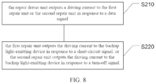
Further, referring to FIG. 8 , the step S200 specifically includes:
S210: the repair driver unit outputs a driving current to the first repair unit or the second repair unit in response to a data signal;
S220: the first repair unit outputs the driving current to the backup light-emitting device in response to a short-circuit signal, or the second repair unit outputs the driving current to the backup light-emitting device in response to a turn-off signal.
Further, the present disclosure further provides a display device, the display device includes a pixel array, and the pixel array includes at least one pixel circuit, in which the pixel circuit includes three sub-pixel repair circuits as described above. The sub-pixel repair circuit is described in detail in the text, and will not be repeated here. By providing the sub-pixel repair circuit in the display device, when the light-emitting device fails, the sub-pixel repair circuit can be utilized to repair the fault effectively, thereby improving the display quality of the display device.
In conclusion, the present disclosure provides a display device, a sub-pixel repair circuit and a repair method thereof. The sub-pixel repair circuit includes a circuit driver module, a circuit detection module, a circuit repair module, a light-emitting device and a backup light-emitting device. The circuit driver module is connected to the scan wire, the data wire, the first power supply terminal, the circuit detection module and the circuit repair module respectively; and the circuit repair module is connected to the first power supply terminal, the positive electrode of the backup light-emitting device, and the circuit detection module; the circuit detection module is connected to the positive electrode of the light-emitting device; the negative electrode of the backup light-emitting device and the negative electrode of the light-emitting device are both connected to the second power supply terminal. The circuit driver module is configured to provide the driving current to the light-emitting device in response to the data signal of the data wire and the scan signal of the scan wire; the circuit repair module is configured to provide the driving current to the backup light-emitting device in response to the data signal provided by the circuit driver module and the short-circuit signal or the turn-off signal provided by the circuit detection module, thereby implementing the fault repairing of the light-emitting device and improving the display quality of the display device.
It can be appreciated that those of ordinary skill in the art can make equivalent replacements or variations according to the technical solution of the present disclosure and the inventive concept thereof, and all these variations or replacements should fall within the protection scope of the appended claims of the present disclosure.

Claims (14)

What is claimed is:
1. A sub-pixel repair circuit, comprising a circuit driver module, a circuit detection module, a circuit repair module, a light-emitting device and a backup light-emitting device; the circuit driver module being connected to a scan wire, a data wire, a first power supply terminal, the circuit detection module and the circuit repair module respectively; the circuit repair module being connected to the first power supply terminal, a positive electrode of the backup light-emitting device, and the circuit detection module; the circuit detection module being connected to a positive electrode of the light-emitting device; a negative electrode of the backup light-emitting device and a negative electrode of the light-emitting device being both connected to a second power supply terminal;
wherein the circuit driver module is configured to provide a driving current to the light-emitting device in response to a data signal of the data wire and a scan signal of the scan wire;
wherein the circuit repair module is configured to provide a driving current to the backup light-emitting device in response to a data signal provided by the circuit driver module and a short-circuit signal or a turn-off signal provided by the circuit detection module;
wherein the circuit repair module comprises a repair driver unit, a first repair unit and a second repair unit the repair driver unit is connected to the first power supply terminal, the first repair unit, the second repair unit and the circuit driver module; the first repair unit is connected to the positive electrode of the backup light-emitting device and the circuit detection module; the second repair unit is connected to the positive electrode of the backup light-emitting device and the circuit detection module;
the repair driver unit is configured to output a driving current to the first repair unit or the second repair unit in response to the data signal;
the first repair unit is configured to output the driving current to the backup light-emitting device in response to the short-circuit signal;
the second repair unit is configured to output the driving current to the backup light-emitting device in response to the turn-off signal.
2. The sub-pixel repair circuit according to claim 1, wherein the circuit detection module comprises a detection resistor; one end of the detection resistor is connected to the circuit driver module and the first repair unit, and the other end of the detection resistor is connected to the second repair unit and the positive electrode of the light-emitting device.
3. The sub-pixel repair circuit according to claim 2, wherein the first repair unit comprises a first switch transistor; a short-circuit signal input terminal of the first switch transistor is connected to one end of the detection resistor, and a driving current input terminal of the first switch transistor is connected to the repair driver unit, and a driving current output terminal of the first switch transistor is connected to a positive electrode of a backup light-emitting device.
4. The sub-pixel repair circuit according to claim 3, wherein the first switch transistor is a P-type transistor.
5. The sub-pixel repair circuit according to claim 2, wherein the second repair unit comprises a second switch transistor; a driving current input terminal of the second switch transistor is connected to the repair driver unit, a turn-off signal input terminal of the second switch transistor is connected to the other end of the detection resistor, and a driving current output terminal of the second switch transistor is connected to the positive electrode of the backup light-emitting device.
6. The sub-pixel repair circuit according to claim 5, wherein the second switch transistor is an N-type transistor.
7. The sub-pixel repair circuit according to claim 2, wherein the repair driver unit comprises a first drive transistor; a data signal input terminal of the first drive transistor is connected to the circuit driver module, a driving current input terminal of the first drive transistor is connected to the first power supply terminal, and a driving current output terminal of the first drive transistor is connected to the first repair unit and the second repair unit.
8. The sub-pixel repair circuit according to claim 7, wherein the first drive transistor is an N-type transistor.
9. The sub-pixel repair circuit according to claim 1, wherein the circuit repair module comprises a second drive transistor, a third switch transistor and an energy storage capacitor; a driving current input terminal of the second drive transistor is connected to the first power supply terminal, a data signal input terminal of the second driving transistor is connected to a data signal output terminal of the third switch transistor, a driving current output terminal of the second drive transistor is connected to the circuit detection module, a data signal input terminal of the third switch transistor is connected to the data wire, a scan signal input terminal of the third switch transistor is connected to the scan wire, a data signal output terminal of the third switch transistor is connected to the circuit repair module, one end of the energy storage capacitor is connected to the first power supply terminal, and the other end of the energy storage capacitor is connected to the data signal output terminal of the third switch transistor and the data signal input terminal of the second drive transistor.
10. The sub-pixel repair circuit according to claim 9, wherein the third switch transistor is an N-type transistor.
11. The sub-pixel repair circuit according to claim 9, wherein the second drive transistor is an N-type transistor.
12. A repair method based on the sub-pixel repair circuit of claim 1, comprising:
when the light-emitting device is turned on, driving, by the circuit driver module, the light-emitting device to illuminate;
when the light-emitting device is shorted or turned off, driving, by the circuit repair module, the backup light-emitting device to illuminate.
13. The repair method for the sub-pixel repair circuit according to claim 12, wherein the driving, by the circuit repair module, the backup light-emitting device to illuminate comprises:
outputting, by a repair driver unit, a driving current to a first repair unit or a second repair unit in response to a data signal;
outputting, by a first repair unit, a driving current to the backup light-emitting device in response to a short-circuit signal; or, outputting, by a second repair unit, the driving current to the backup light-emitting device in response to a turn-off signal.
14. A display device, comprising a pixel array, wherein the pixel array comprises at least one pixel circuit, and the pixel circuit comprises three sub-pixel repair circuits of claim 1.
US17/725,862 2020-06-23 2022-04-21 Display device, sub-pixel repair circuit and repair method therefor Active US11763733B2 (en)

Applications Claiming Priority (1)

Application Number Priority Date Filing Date Title
PCT/CN2020/097702 WO2021258283A1 (en) 2020-06-23 2020-06-23 Display device, sub-pixel repair circuit and repair method therefor

Related Parent Applications (1)

Application Number Title Priority Date Filing Date
PCT/CN2020/097702 Continuation WO2021258283A1 (en) 2020-06-23 2020-06-23 Display device, sub-pixel repair circuit and repair method therefor

Publications (2)

Publication Number Publication Date
US20220246091A1 US20220246091A1 (en) 2022-08-04
US11763733B2 true US11763733B2 (en) 2023-09-19

Family

ID=79282658

Family Applications (1)

Application Number Title Priority Date Filing Date
US17/725,862 Active US11763733B2 (en) 2020-06-23 2022-04-21 Display device, sub-pixel repair circuit and repair method therefor

Country Status (2)

Country Link
US (1) US11763733B2 (en)
WO (1) WO2021258283A1 (en)

Families Citing this family (4)

* Cited by examiner, † Cited by third party
Publication number Priority date Publication date Assignee Title
US20220148928A1 (en) * 2020-11-11 2022-05-12 Chongqing Konka Photoelectric Technology Research Institute Co., Ltd. Detection method and detection structure for display backplane
CN119604917A (en) * 2023-04-23 2025-03-11 京东方科技集团股份有限公司 Display substrate and detection method thereof, and display device
WO2024243743A1 (en) * 2023-05-26 2024-12-05 京东方科技集团股份有限公司 Pixel circuit, array substrate, and display panel
TWI894999B (en) * 2024-06-07 2025-08-21 友達光電股份有限公司 Micro led panel, operation method and pixel compensation circuit

Citations (15)

* Cited by examiner, † Cited by third party
Publication number Priority date Publication date Assignee Title
CN101833916A (en) 2009-09-01 2010-09-15 友达光电股份有限公司 Pixel driving circuit for light-emitting display panel
US20150123884A1 (en) 2013-11-06 2015-05-07 Samsung Display Co., Ltd. Organic light emitting display apparatus
US20160012773A1 (en) * 2014-07-08 2016-01-14 Samsung Display Co., Ltd. Organic light-emitting diode (oled) display panel and oled display having the same
CN106251798A (en) 2016-08-08 2016-12-21 深圳市华星光电技术有限公司 OLED display drive circuit defect inspection method
US20170032722A1 (en) 2015-07-28 2017-02-02 Samsung Display Co., Ltd. Organic light emitting display device and repairing method thereof
CN108962106A (en) 2018-07-13 2018-12-07 京东方科技集团股份有限公司 A kind of pixel detection circuit, display base plate and pixel detecting method
CN109697956A (en) 2017-10-24 2019-04-30 乐金显示有限公司 Organic light-emitting display device and its driving method
CN110047425A (en) 2019-05-17 2019-07-23 京东方科技集团股份有限公司 Pixel circuit and its control method, display panel
CN110097842A (en) 2019-01-25 2019-08-06 友达光电股份有限公司 Pixel circuit and its detection method
US10461123B2 (en) * 2016-12-21 2019-10-29 Samsung Display Co., Ltd. Light emitting device and display device including the same
CN110415643A (en) 2019-08-29 2019-11-05 南京浣轩半导体有限公司 A kind of adaptive elimination LED ghost and coupling and the circuit and method of protecting self-test
CN111091780A (en) 2019-01-31 2020-05-01 友达光电股份有限公司 Pixel circuit and its repairing method
CN111145684A (en) 2020-02-17 2020-05-12 重庆康佳光电技术研究院有限公司 Pixel circuit, display substrate and display device
US20220302354A1 (en) * 2021-03-16 2022-09-22 Samsung Display Co., Ltd. Display device
US20220327996A1 (en) * 2019-09-05 2022-10-13 Boe Technology Group Co., Ltd. Pixel driving circuit, pixel driving method, display apparatus and method for controlling the same

Patent Citations (18)

* Cited by examiner, † Cited by third party
Publication number Priority date Publication date Assignee Title
CN101833916A (en) 2009-09-01 2010-09-15 友达光电股份有限公司 Pixel driving circuit for light-emitting display panel
US20150123884A1 (en) 2013-11-06 2015-05-07 Samsung Display Co., Ltd. Organic light emitting display apparatus
US9747835B2 (en) * 2014-07-08 2017-08-29 Samsung Display Co., Ltd. Organic light-emitting diode (OLED) display panel and OLED display having the same
US20160012773A1 (en) * 2014-07-08 2016-01-14 Samsung Display Co., Ltd. Organic light-emitting diode (oled) display panel and oled display having the same
US10510277B2 (en) * 2015-07-28 2019-12-17 Samsung Display Co., Ltd. Organic light emitting display device and repairing method thereof
US20170032722A1 (en) 2015-07-28 2017-02-02 Samsung Display Co., Ltd. Organic light emitting display device and repairing method thereof
CN106251798A (en) 2016-08-08 2016-12-21 深圳市华星光电技术有限公司 OLED display drive circuit defect inspection method
US10461123B2 (en) * 2016-12-21 2019-10-29 Samsung Display Co., Ltd. Light emitting device and display device including the same
CN109697956A (en) 2017-10-24 2019-04-30 乐金显示有限公司 Organic light-emitting display device and its driving method
CN108962106A (en) 2018-07-13 2018-12-07 京东方科技集团股份有限公司 A kind of pixel detection circuit, display base plate and pixel detecting method
CN110097842A (en) 2019-01-25 2019-08-06 友达光电股份有限公司 Pixel circuit and its detection method
CN111091780B (en) 2019-01-31 2021-04-30 友达光电股份有限公司 Pixel circuit and repairing method thereof
CN111091780A (en) 2019-01-31 2020-05-01 友达光电股份有限公司 Pixel circuit and its repairing method
CN110047425A (en) 2019-05-17 2019-07-23 京东方科技集团股份有限公司 Pixel circuit and its control method, display panel
CN110415643A (en) 2019-08-29 2019-11-05 南京浣轩半导体有限公司 A kind of adaptive elimination LED ghost and coupling and the circuit and method of protecting self-test
US20220327996A1 (en) * 2019-09-05 2022-10-13 Boe Technology Group Co., Ltd. Pixel driving circuit, pixel driving method, display apparatus and method for controlling the same
CN111145684A (en) 2020-02-17 2020-05-12 重庆康佳光电技术研究院有限公司 Pixel circuit, display substrate and display device
US20220302354A1 (en) * 2021-03-16 2022-09-22 Samsung Display Co., Ltd. Display device

Non-Patent Citations (3)

* Cited by examiner, † Cited by third party
Title
Patent Cooperation Treaty: China International Property AdminisliaLion (ISA/CN): International Search Report and Written Opinion of PCT/CN2020/097702 (related application); dated Mar. 17, 2021; 12 pages (including translation).
The State Intellectual Property Office of People's Republic of China: The First Office Action of Chinese Patent Application No. 202010578830.8, dated Dec. 28, 2021, Ying Feng; 16 pages (including translation).
The State Intellectual Property Office of People's Republic of China: The Second Office Action of Chinese Patent Application No. 202010578830.8, dated Feb. 21, 2022, Ying Feng; 9 pages (including translation).

Also Published As

Publication number Publication date
US20220246091A1 (en) 2022-08-04
WO2021258283A1 (en) 2021-12-30

Similar Documents

Publication Publication Date Title
US11763733B2 (en) Display device, sub-pixel repair circuit and repair method therefor
US10580360B2 (en) Pixel circuit and driving method thereof, display device
US10657887B2 (en) Protection circuit and method, pixel circuit, and display device
CN110689840B (en) Pixel circuit, short circuit detection method and display panel
US8963907B2 (en) Pixel circuit and driving method thereof
CN106531079B (en) Pixel circuit and driving method thereof, display device
US11741883B2 (en) Pixel circuit, control method thereof and display panel
CN111477166A (en) Pixel circuit, pixel driving method and display device
CN112669765B (en) Breakpoint self-repairing pixel driving circuit, driving method and display device
US11222594B2 (en) Digital pixel driving circuit and digital pixel driving method
US20210097908A1 (en) Light emitting control circuit, driving method thereof, array substrate and display device
CN108682385B (en) Pixel circuit, pixel driving method and display device
CN109064985B (en) Overcurrent protection circuit and display device
CN110517631B (en) Pixel driving circuit, display panel and driving method of pixel driving circuit
CN114863879B (en) Organic light emitting diode control circuit and display panel
CN113450697B (en) Display device, brightness compensation circuit and compensation method thereof
US11996057B2 (en) Backlight module and display device
CN210142496U (en) Pixel driving circuit and display panel
CN206271396U (en) A pixel circuit and display device
CN113450698B (en) Display device, sub-pixel repair circuit and repair method thereof
CN206282593U (en) A kind of image element circuit and display device
WO2022156195A1 (en) Test board
CN111199712A (en) Pixel compensation circuit and display device
CN114203103A (en) Light-emitting circuit, backlight module and display panel
CN211350063U (en) Pixel circuit, display substrate and display device

Legal Events

Date Code Title Description
AS Assignment

Owner name: CHONGQING KONKA PHOTOELECTRIC TECHNOLOGY RESEARCH INSTITUTE CO., LTD., CHINA

Free format text: ASSIGNMENT OF ASSIGNORS INTEREST;ASSIGNORS:YIN, CHAOWEI;FENG, ZHONGSHAN;REEL/FRAME:059666/0810

Effective date: 20220406

FEPP Fee payment procedure

Free format text: ENTITY STATUS SET TO UNDISCOUNTED (ORIGINAL EVENT CODE: BIG.); ENTITY STATUS OF PATENT OWNER: SMALL ENTITY

FEPP Fee payment procedure

Free format text: ENTITY STATUS SET TO SMALL (ORIGINAL EVENT CODE: SMAL); ENTITY STATUS OF PATENT OWNER: SMALL ENTITY

STPP Information on status: patent application and granting procedure in general

Free format text: DOCKETED NEW CASE - READY FOR EXAMINATION

STPP Information on status: patent application and granting procedure in general

Free format text: RESPONSE TO NON-FINAL OFFICE ACTION ENTERED AND FORWARDED TO EXAMINER

STPP Information on status: patent application and granting procedure in general

Free format text: PUBLICATIONS -- ISSUE FEE PAYMENT VERIFIED

STCF Information on status: patent grant

Free format text: PATENTED CASE