US11753721B2 - Transition-metal chalcogenide thin film and preparing method of the same - Google Patents
Transition-metal chalcogenide thin film and preparing method of the same Download PDFInfo
- Publication number
- US11753721B2 US11753721B2 US17/116,053 US202017116053A US11753721B2 US 11753721 B2 US11753721 B2 US 11753721B2 US 202017116053 A US202017116053 A US 202017116053A US 11753721 B2 US11753721 B2 US 11753721B2
- Authority
- US
- United States
- Prior art keywords
- transition metal
- metal chalcogenide
- precursor
- thin film
- thin films
- Prior art date
- Legal status (The legal status is an assumption and is not a legal conclusion. Google has not performed a legal analysis and makes no representation as to the accuracy of the status listed.)
- Active
Links
- -1 Transition-metal chalcogenide Chemical class 0.000 title claims abstract description 244
- 229910052723 transition metal Inorganic materials 0.000 title claims abstract description 232
- 239000010409 thin film Substances 0.000 title claims abstract description 197
- 238000000034 method Methods 0.000 title claims description 41
- 239000002243 precursor Substances 0.000 claims abstract description 119
- 238000004519 manufacturing process Methods 0.000 claims abstract description 91
- 239000000758 substrate Substances 0.000 claims abstract description 80
- 239000003446 ligand Substances 0.000 claims abstract description 33
- 150000001412 amines Chemical class 0.000 claims abstract description 23
- 230000001678 irradiating effect Effects 0.000 claims abstract description 21
- ZMXDDKWLCZADIW-UHFFFAOYSA-N N,N-Dimethylformamide Chemical compound CN(C)C=O ZMXDDKWLCZADIW-UHFFFAOYSA-N 0.000 claims description 29
- OAKJQQAXSVQMHS-UHFFFAOYSA-N Hydrazine Chemical compound NN OAKJQQAXSVQMHS-UHFFFAOYSA-N 0.000 claims description 22
- VYPSYNLAJGMNEJ-UHFFFAOYSA-N Silicium dioxide Chemical compound O=[Si]=O VYPSYNLAJGMNEJ-UHFFFAOYSA-N 0.000 claims description 22
- HZAXFHJVJLSVMW-UHFFFAOYSA-N 2-Aminoethan-1-ol Chemical compound NCCO HZAXFHJVJLSVMW-UHFFFAOYSA-N 0.000 claims description 20
- 239000000463 material Substances 0.000 claims description 16
- IAZDPXIOMUYVGZ-UHFFFAOYSA-N Dimethylsulphoxide Chemical compound CS(C)=O IAZDPXIOMUYVGZ-UHFFFAOYSA-N 0.000 claims description 12
- 238000004528 spin coating Methods 0.000 claims description 12
- 229910052681 coesite Inorganic materials 0.000 claims description 11
- 229910052906 cristobalite Inorganic materials 0.000 claims description 11
- 229910052711 selenium Inorganic materials 0.000 claims description 11
- 239000000377 silicon dioxide Substances 0.000 claims description 11
- 229910052682 stishovite Inorganic materials 0.000 claims description 11
- 229910052905 tridymite Inorganic materials 0.000 claims description 11
- 229910052717 sulfur Inorganic materials 0.000 claims description 10
- LYCAIKOWRPUZTN-UHFFFAOYSA-N Ethylene glycol Chemical compound OCCO LYCAIKOWRPUZTN-UHFFFAOYSA-N 0.000 claims description 9
- 229910052738 indium Inorganic materials 0.000 claims description 9
- PIICEJLVQHRZGT-UHFFFAOYSA-N Ethylenediamine Chemical compound NCCN PIICEJLVQHRZGT-UHFFFAOYSA-N 0.000 claims description 8
- 229910052787 antimony Inorganic materials 0.000 claims description 8
- 229910052785 arsenic Inorganic materials 0.000 claims description 8
- 229910052797 bismuth Inorganic materials 0.000 claims description 8
- 229910052733 gallium Inorganic materials 0.000 claims description 8
- 229910052732 germanium Inorganic materials 0.000 claims description 8
- 229910052735 hafnium Inorganic materials 0.000 claims description 8
- 229910052748 manganese Inorganic materials 0.000 claims description 8
- 229910052750 molybdenum Inorganic materials 0.000 claims description 8
- 229910052702 rhenium Inorganic materials 0.000 claims description 8
- 229910052715 tantalum Inorganic materials 0.000 claims description 8
- 229910052714 tellurium Inorganic materials 0.000 claims description 8
- 229910052718 tin Inorganic materials 0.000 claims description 8
- 229910052719 titanium Inorganic materials 0.000 claims description 8
- 229910052721 tungsten Inorganic materials 0.000 claims description 8
- 229910052720 vanadium Inorganic materials 0.000 claims description 8
- 229910052725 zinc Inorganic materials 0.000 claims description 8
- RTZKZFJDLAIYFH-UHFFFAOYSA-N Diethyl ether Chemical compound CCOCC RTZKZFJDLAIYFH-UHFFFAOYSA-N 0.000 claims description 6
- SECXISVLQFMRJM-UHFFFAOYSA-N N-Methylpyrrolidone Chemical compound CN1CCCC1=O SECXISVLQFMRJM-UHFFFAOYSA-N 0.000 claims description 6
- WYURNTSHIVDZCO-UHFFFAOYSA-N Tetrahydrofuran Chemical compound C1CCOC1 WYURNTSHIVDZCO-UHFFFAOYSA-N 0.000 claims description 6
- MCMNRKCIXSYSNV-UHFFFAOYSA-N Zirconium dioxide Chemical compound O=[Zr]=O MCMNRKCIXSYSNV-UHFFFAOYSA-N 0.000 claims description 6
- 238000010438 heat treatment Methods 0.000 claims description 6
- 238000007639 printing Methods 0.000 claims description 6
- 239000011248 coating agent Substances 0.000 claims description 4
- 238000000576 coating method Methods 0.000 claims description 4
- 238000007641 inkjet printing Methods 0.000 claims description 4
- 238000000059 patterning Methods 0.000 claims description 4
- VYMPLPIFKRHAAC-UHFFFAOYSA-N 1,2-ethanedithiol Chemical compound SCCS VYMPLPIFKRHAAC-UHFFFAOYSA-N 0.000 claims description 3
- 229910017083 AlN Inorganic materials 0.000 claims description 3
- 229920000089 Cyclic olefin copolymer Polymers 0.000 claims description 3
- 239000004713 Cyclic olefin copolymer Substances 0.000 claims description 3
- 229920001046 Nanocellulose Polymers 0.000 claims description 3
- 239000004952 Polyamide Substances 0.000 claims description 3
- 239000004695 Polyether sulfone Substances 0.000 claims description 3
- 239000004697 Polyetherimide Substances 0.000 claims description 3
- 239000004698 Polyethylene Substances 0.000 claims description 3
- 239000004642 Polyimide Substances 0.000 claims description 3
- 239000004743 Polypropylene Substances 0.000 claims description 3
- 239000004793 Polystyrene Substances 0.000 claims description 3
- 239000004372 Polyvinyl alcohol Substances 0.000 claims description 3
- 229910052581 Si3N4 Inorganic materials 0.000 claims description 3
- UCKMPCXJQFINFW-UHFFFAOYSA-N Sulphide Chemical compound [S-2] UCKMPCXJQFINFW-UHFFFAOYSA-N 0.000 claims description 3
- PNEYBMLMFCGWSK-UHFFFAOYSA-N aluminium oxide Inorganic materials [O-2].[O-2].[O-2].[Al+3].[Al+3] PNEYBMLMFCGWSK-UHFFFAOYSA-N 0.000 claims description 3
- 239000000919 ceramic Substances 0.000 claims description 3
- 229910052593 corundum Inorganic materials 0.000 claims description 3
- 239000004205 dimethyl polysiloxane Substances 0.000 claims description 3
- 238000007646 gravure printing Methods 0.000 claims description 3
- GNOIPBMMFNIUFM-UHFFFAOYSA-N hexamethylphosphoric triamide Chemical compound CN(C)P(=O)(N(C)C)N(C)C GNOIPBMMFNIUFM-UHFFFAOYSA-N 0.000 claims description 3
- JEIPFZHSYJVQDO-UHFFFAOYSA-N iron(III) oxide Inorganic materials O=[Fe]O[Fe]=O JEIPFZHSYJVQDO-UHFFFAOYSA-N 0.000 claims description 3
- 229910003465 moissanite Inorganic materials 0.000 claims description 3
- 230000005693 optoelectronics Effects 0.000 claims description 3
- 229920000435 poly(dimethylsiloxane) Polymers 0.000 claims description 3
- 229920003207 poly(ethylene-2,6-naphthalate) Polymers 0.000 claims description 3
- 229920000636 poly(norbornene) polymer Polymers 0.000 claims description 3
- 229920000058 polyacrylate Polymers 0.000 claims description 3
- 229920002647 polyamide Polymers 0.000 claims description 3
- 229920001230 polyarylate Polymers 0.000 claims description 3
- 229920001707 polybutylene terephthalate Polymers 0.000 claims description 3
- 239000004417 polycarbonate Substances 0.000 claims description 3
- 229920000515 polycarbonate Polymers 0.000 claims description 3
- 229920006393 polyether sulfone Polymers 0.000 claims description 3
- 229920001601 polyetherimide Polymers 0.000 claims description 3
- 229920000573 polyethylene Polymers 0.000 claims description 3
- 239000011112 polyethylene naphthalate Substances 0.000 claims description 3
- 229920000139 polyethylene terephthalate Polymers 0.000 claims description 3
- 239000005020 polyethylene terephthalate Substances 0.000 claims description 3
- 229920001721 polyimide Polymers 0.000 claims description 3
- 229920000642 polymer Polymers 0.000 claims description 3
- 229920000193 polymethacrylate Polymers 0.000 claims description 3
- 229920006389 polyphenyl polymer Polymers 0.000 claims description 3
- 229920001155 polypropylene Polymers 0.000 claims description 3
- 229920002223 polystyrene Polymers 0.000 claims description 3
- 229920002451 polyvinyl alcohol Polymers 0.000 claims description 3
- 238000007650 screen-printing Methods 0.000 claims description 3
- 229910010271 silicon carbide Inorganic materials 0.000 claims description 3
- 238000007764 slot die coating Methods 0.000 claims description 3
- 239000002904 solvent Substances 0.000 claims description 3
- 238000005507 spraying Methods 0.000 claims description 3
- 229910001845 yogo sapphire Inorganic materials 0.000 claims description 3
- XLOMVQKBTHCTTD-UHFFFAOYSA-N zinc oxide Inorganic materials [Zn]=O XLOMVQKBTHCTTD-UHFFFAOYSA-N 0.000 claims description 3
- 238000001035 drying Methods 0.000 claims 3
- 238000000354 decomposition reaction Methods 0.000 claims 2
- 229920000307 polymer substrate Polymers 0.000 claims 2
- 239000000243 solution Substances 0.000 description 32
- 239000011669 selenium Substances 0.000 description 19
- 229910005641 SnSx Inorganic materials 0.000 description 16
- 238000001237 Raman spectrum Methods 0.000 description 14
- 229910052961 molybdenite Inorganic materials 0.000 description 14
- 229910052982 molybdenum disulfide Inorganic materials 0.000 description 14
- 230000008569 process Effects 0.000 description 13
- CWQXQMHSOZUFJS-UHFFFAOYSA-N molybdenum disulfide Chemical compound S=[Mo]=S CWQXQMHSOZUFJS-UHFFFAOYSA-N 0.000 description 12
- 239000013078 crystal Substances 0.000 description 11
- 229920003023 plastic Polymers 0.000 description 10
- 239000004033 plastic Substances 0.000 description 10
- 150000001787 chalcogens Chemical group 0.000 description 9
- 150000004770 chalcogenides Chemical class 0.000 description 7
- 239000000203 mixture Substances 0.000 description 7
- 238000012546 transfer Methods 0.000 description 7
- NWZSZGALRFJKBT-KNIFDHDWSA-N (2s)-2,6-diaminohexanoic acid;(2s)-2-hydroxybutanedioic acid Chemical compound OC(=O)[C@@H](O)CC(O)=O.NCCCC[C@H](N)C(O)=O NWZSZGALRFJKBT-KNIFDHDWSA-N 0.000 description 6
- 229910052798 chalcogen Inorganic materials 0.000 description 6
- 230000018044 dehydration Effects 0.000 description 6
- 238000006297 dehydration reaction Methods 0.000 description 6
- IKDUDTNKRLTJSI-UHFFFAOYSA-N hydrazine monohydrate Substances O.NN IKDUDTNKRLTJSI-UHFFFAOYSA-N 0.000 description 6
- 229910052751 metal Inorganic materials 0.000 description 6
- 239000002184 metal Substances 0.000 description 6
- 239000000126 substance Substances 0.000 description 6
- 230000000052 comparative effect Effects 0.000 description 5
- 230000008901 benefit Effects 0.000 description 4
- 238000010586 diagram Methods 0.000 description 4
- 238000012545 processing Methods 0.000 description 4
- 150000003624 transition metals Chemical class 0.000 description 4
- BUGBHKTXTAQXES-UHFFFAOYSA-N Selenium Chemical compound [Se] BUGBHKTXTAQXES-UHFFFAOYSA-N 0.000 description 3
- 230000015572 biosynthetic process Effects 0.000 description 3
- 238000000724 energy-dispersive X-ray spectrum Methods 0.000 description 3
- 239000002861 polymer material Substances 0.000 description 3
- 239000002244 precipitate Substances 0.000 description 3
- 229910019964 (NH4)2MoS4 Inorganic materials 0.000 description 2
- NINIDFKCEFEMDL-UHFFFAOYSA-N Sulfur Chemical compound [S] NINIDFKCEFEMDL-UHFFFAOYSA-N 0.000 description 2
- 238000010924 continuous production Methods 0.000 description 2
- 238000002425 crystallisation Methods 0.000 description 2
- 230000008025 crystallization Effects 0.000 description 2
- 238000002524 electron diffraction data Methods 0.000 description 2
- 238000002149 energy-dispersive X-ray emission spectroscopy Methods 0.000 description 2
- 239000011259 mixed solution Substances 0.000 description 2
- 238000011112 process operation Methods 0.000 description 2
- 230000009257 reactivity Effects 0.000 description 2
- 238000000926 separation method Methods 0.000 description 2
- 230000007928 solubilization Effects 0.000 description 2
- 238000005063 solubilization Methods 0.000 description 2
- 239000011593 sulfur Substances 0.000 description 2
- 230000007704 transition Effects 0.000 description 2
- OKTJSMMVPCPJKN-UHFFFAOYSA-N Carbon Chemical compound [C] OKTJSMMVPCPJKN-UHFFFAOYSA-N 0.000 description 1
- 230000007547 defect Effects 0.000 description 1
- 230000000694 effects Effects 0.000 description 1
- 239000010408 film Substances 0.000 description 1
- 229910021389 graphene Inorganic materials 0.000 description 1
- 239000012535 impurity Substances 0.000 description 1
- APFVFJFRJDLVQX-UHFFFAOYSA-N indium atom Chemical compound [In] APFVFJFRJDLVQX-UHFFFAOYSA-N 0.000 description 1
- 230000008018 melting Effects 0.000 description 1
- 238000002844 melting Methods 0.000 description 1
- 230000004048 modification Effects 0.000 description 1
- 238000012986 modification Methods 0.000 description 1
- 238000011160 research Methods 0.000 description 1
- 238000001228 spectrum Methods 0.000 description 1
- 230000000087 stabilizing effect Effects 0.000 description 1
- AFNRRBXCCXDRPS-UHFFFAOYSA-N tin(ii) sulfide Chemical compound [Sn]=S AFNRRBXCCXDRPS-UHFFFAOYSA-N 0.000 description 1
Images


Classifications
-
- C—CHEMISTRY; METALLURGY
- C23—COATING METALLIC MATERIAL; COATING MATERIAL WITH METALLIC MATERIAL; CHEMICAL SURFACE TREATMENT; DIFFUSION TREATMENT OF METALLIC MATERIAL; COATING BY VACUUM EVAPORATION, BY SPUTTERING, BY ION IMPLANTATION OR BY CHEMICAL VAPOUR DEPOSITION, IN GENERAL; INHIBITING CORROSION OF METALLIC MATERIAL OR INCRUSTATION IN GENERAL
- C23C—COATING METALLIC MATERIAL; COATING MATERIAL WITH METALLIC MATERIAL; SURFACE TREATMENT OF METALLIC MATERIAL BY DIFFUSION INTO THE SURFACE, BY CHEMICAL CONVERSION OR SUBSTITUTION; COATING BY VACUUM EVAPORATION, BY SPUTTERING, BY ION IMPLANTATION OR BY CHEMICAL VAPOUR DEPOSITION, IN GENERAL
- C23C18/00—Chemical coating by decomposition of either liquid compounds or solutions of the coating forming compounds, without leaving reaction products of surface material in the coating; Contact plating
- C23C18/14—Decomposition by irradiation, e.g. photolysis, particle radiation or by mixed irradiation sources
- C23C18/143—Radiation by light, e.g. photolysis or pyrolysis
-
- C—CHEMISTRY; METALLURGY
- C23—COATING METALLIC MATERIAL; COATING MATERIAL WITH METALLIC MATERIAL; CHEMICAL SURFACE TREATMENT; DIFFUSION TREATMENT OF METALLIC MATERIAL; COATING BY VACUUM EVAPORATION, BY SPUTTERING, BY ION IMPLANTATION OR BY CHEMICAL VAPOUR DEPOSITION, IN GENERAL; INHIBITING CORROSION OF METALLIC MATERIAL OR INCRUSTATION IN GENERAL
- C23C—COATING METALLIC MATERIAL; COATING MATERIAL WITH METALLIC MATERIAL; SURFACE TREATMENT OF METALLIC MATERIAL BY DIFFUSION INTO THE SURFACE, BY CHEMICAL CONVERSION OR SUBSTITUTION; COATING BY VACUUM EVAPORATION, BY SPUTTERING, BY ION IMPLANTATION OR BY CHEMICAL VAPOUR DEPOSITION, IN GENERAL
- C23C18/00—Chemical coating by decomposition of either liquid compounds or solutions of the coating forming compounds, without leaving reaction products of surface material in the coating; Contact plating
- C23C18/02—Chemical coating by decomposition of either liquid compounds or solutions of the coating forming compounds, without leaving reaction products of surface material in the coating; Contact plating by thermal decomposition
- C23C18/12—Chemical coating by decomposition of either liquid compounds or solutions of the coating forming compounds, without leaving reaction products of surface material in the coating; Contact plating by thermal decomposition characterised by the deposition of inorganic material other than metallic material
- C23C18/1204—Chemical coating by decomposition of either liquid compounds or solutions of the coating forming compounds, without leaving reaction products of surface material in the coating; Contact plating by thermal decomposition characterised by the deposition of inorganic material other than metallic material inorganic material, e.g. non-oxide and non-metallic such as sulfides, nitrides based compounds
-
- C—CHEMISTRY; METALLURGY
- C23—COATING METALLIC MATERIAL; COATING MATERIAL WITH METALLIC MATERIAL; CHEMICAL SURFACE TREATMENT; DIFFUSION TREATMENT OF METALLIC MATERIAL; COATING BY VACUUM EVAPORATION, BY SPUTTERING, BY ION IMPLANTATION OR BY CHEMICAL VAPOUR DEPOSITION, IN GENERAL; INHIBITING CORROSION OF METALLIC MATERIAL OR INCRUSTATION IN GENERAL
- C23C—COATING METALLIC MATERIAL; COATING MATERIAL WITH METALLIC MATERIAL; SURFACE TREATMENT OF METALLIC MATERIAL BY DIFFUSION INTO THE SURFACE, BY CHEMICAL CONVERSION OR SUBSTITUTION; COATING BY VACUUM EVAPORATION, BY SPUTTERING, BY ION IMPLANTATION OR BY CHEMICAL VAPOUR DEPOSITION, IN GENERAL
- C23C18/00—Chemical coating by decomposition of either liquid compounds or solutions of the coating forming compounds, without leaving reaction products of surface material in the coating; Contact plating
- C23C18/02—Chemical coating by decomposition of either liquid compounds or solutions of the coating forming compounds, without leaving reaction products of surface material in the coating; Contact plating by thermal decomposition
- C23C18/04—Pretreatment of the material to be coated
-
- C—CHEMISTRY; METALLURGY
- C23—COATING METALLIC MATERIAL; COATING MATERIAL WITH METALLIC MATERIAL; CHEMICAL SURFACE TREATMENT; DIFFUSION TREATMENT OF METALLIC MATERIAL; COATING BY VACUUM EVAPORATION, BY SPUTTERING, BY ION IMPLANTATION OR BY CHEMICAL VAPOUR DEPOSITION, IN GENERAL; INHIBITING CORROSION OF METALLIC MATERIAL OR INCRUSTATION IN GENERAL
- C23C—COATING METALLIC MATERIAL; COATING MATERIAL WITH METALLIC MATERIAL; SURFACE TREATMENT OF METALLIC MATERIAL BY DIFFUSION INTO THE SURFACE, BY CHEMICAL CONVERSION OR SUBSTITUTION; COATING BY VACUUM EVAPORATION, BY SPUTTERING, BY ION IMPLANTATION OR BY CHEMICAL VAPOUR DEPOSITION, IN GENERAL
- C23C18/00—Chemical coating by decomposition of either liquid compounds or solutions of the coating forming compounds, without leaving reaction products of surface material in the coating; Contact plating
- C23C18/02—Chemical coating by decomposition of either liquid compounds or solutions of the coating forming compounds, without leaving reaction products of surface material in the coating; Contact plating by thermal decomposition
- C23C18/06—Coating on selected surface areas, e.g. using masks
-
- C—CHEMISTRY; METALLURGY
- C23—COATING METALLIC MATERIAL; COATING MATERIAL WITH METALLIC MATERIAL; CHEMICAL SURFACE TREATMENT; DIFFUSION TREATMENT OF METALLIC MATERIAL; COATING BY VACUUM EVAPORATION, BY SPUTTERING, BY ION IMPLANTATION OR BY CHEMICAL VAPOUR DEPOSITION, IN GENERAL; INHIBITING CORROSION OF METALLIC MATERIAL OR INCRUSTATION IN GENERAL
- C23C—COATING METALLIC MATERIAL; COATING MATERIAL WITH METALLIC MATERIAL; SURFACE TREATMENT OF METALLIC MATERIAL BY DIFFUSION INTO THE SURFACE, BY CHEMICAL CONVERSION OR SUBSTITUTION; COATING BY VACUUM EVAPORATION, BY SPUTTERING, BY ION IMPLANTATION OR BY CHEMICAL VAPOUR DEPOSITION, IN GENERAL
- C23C18/00—Chemical coating by decomposition of either liquid compounds or solutions of the coating forming compounds, without leaving reaction products of surface material in the coating; Contact plating
- C23C18/02—Chemical coating by decomposition of either liquid compounds or solutions of the coating forming compounds, without leaving reaction products of surface material in the coating; Contact plating by thermal decomposition
- C23C18/12—Chemical coating by decomposition of either liquid compounds or solutions of the coating forming compounds, without leaving reaction products of surface material in the coating; Contact plating by thermal decomposition characterised by the deposition of inorganic material other than metallic material
- C23C18/1229—Composition of the substrate
- C23C18/1233—Organic substrates
-
- C—CHEMISTRY; METALLURGY
- C23—COATING METALLIC MATERIAL; COATING MATERIAL WITH METALLIC MATERIAL; CHEMICAL SURFACE TREATMENT; DIFFUSION TREATMENT OF METALLIC MATERIAL; COATING BY VACUUM EVAPORATION, BY SPUTTERING, BY ION IMPLANTATION OR BY CHEMICAL VAPOUR DEPOSITION, IN GENERAL; INHIBITING CORROSION OF METALLIC MATERIAL OR INCRUSTATION IN GENERAL
- C23C—COATING METALLIC MATERIAL; COATING MATERIAL WITH METALLIC MATERIAL; SURFACE TREATMENT OF METALLIC MATERIAL BY DIFFUSION INTO THE SURFACE, BY CHEMICAL CONVERSION OR SUBSTITUTION; COATING BY VACUUM EVAPORATION, BY SPUTTERING, BY ION IMPLANTATION OR BY CHEMICAL VAPOUR DEPOSITION, IN GENERAL
- C23C18/00—Chemical coating by decomposition of either liquid compounds or solutions of the coating forming compounds, without leaving reaction products of surface material in the coating; Contact plating
- C23C18/02—Chemical coating by decomposition of either liquid compounds or solutions of the coating forming compounds, without leaving reaction products of surface material in the coating; Contact plating by thermal decomposition
- C23C18/12—Chemical coating by decomposition of either liquid compounds or solutions of the coating forming compounds, without leaving reaction products of surface material in the coating; Contact plating by thermal decomposition characterised by the deposition of inorganic material other than metallic material
- C23C18/1229—Composition of the substrate
- C23C18/1245—Inorganic substrates other than metallic
-
- C—CHEMISTRY; METALLURGY
- C23—COATING METALLIC MATERIAL; COATING MATERIAL WITH METALLIC MATERIAL; CHEMICAL SURFACE TREATMENT; DIFFUSION TREATMENT OF METALLIC MATERIAL; COATING BY VACUUM EVAPORATION, BY SPUTTERING, BY ION IMPLANTATION OR BY CHEMICAL VAPOUR DEPOSITION, IN GENERAL; INHIBITING CORROSION OF METALLIC MATERIAL OR INCRUSTATION IN GENERAL
- C23C—COATING METALLIC MATERIAL; COATING MATERIAL WITH METALLIC MATERIAL; SURFACE TREATMENT OF METALLIC MATERIAL BY DIFFUSION INTO THE SURFACE, BY CHEMICAL CONVERSION OR SUBSTITUTION; COATING BY VACUUM EVAPORATION, BY SPUTTERING, BY ION IMPLANTATION OR BY CHEMICAL VAPOUR DEPOSITION, IN GENERAL
- C23C18/00—Chemical coating by decomposition of either liquid compounds or solutions of the coating forming compounds, without leaving reaction products of surface material in the coating; Contact plating
- C23C18/02—Chemical coating by decomposition of either liquid compounds or solutions of the coating forming compounds, without leaving reaction products of surface material in the coating; Contact plating by thermal decomposition
- C23C18/12—Chemical coating by decomposition of either liquid compounds or solutions of the coating forming compounds, without leaving reaction products of surface material in the coating; Contact plating by thermal decomposition characterised by the deposition of inorganic material other than metallic material
- C23C18/125—Process of deposition of the inorganic material
Definitions
- the present disclosure relates to transition metal chalcogenide thin films and a manufacturing method thereof.
- Transition metal chalcogenides have the advantage of having a band gap compared to graphene, i.e., an existing two-dimensional device. Particularly, transition metal chalcogenides have advantages that band gaps of transition metal chalcogenides are different depending on types of elements constituting transition metal chalcogenides, transition metal chalcogenides can be controlled from an indirect transition to a direct transition band depending on thickness, and a material itself of transition metal chalcogenides has a very thin thickness. Due to these advantages, transition metal chalcogenides can be variously applied to transistors, various integrated circuits, optoelectronic devices, gas sensors, wearable devices, etc.
- Korean registered patent No. 10-1623791 discloses a method of directly forming transition metal chalcogenide thin films on a substrate.
- a problem still remains that types of usable substrates are limited because high-temperature heat treatment is required.
- a method of manufacturing transition metal chalcogenide thin films includes the operations of: forming a transition metal chalcogenides precursor on a substrate; and irradiating light onto the transition metal chalcogenides precursor.
- the transition metal chalcogenides precursor includes an amine-based ligand.
- the transition metal chalcogenides precursor may include a material represented by LMX n+m , where the M is Mo, In, W, Hf, V, Sn, Re, Ta, Zn, Ga, Ge, Mn, As, Sb, Bi or Ti, the L is an amine-based ligand coordinated to the M, the X is S, Se or Te, the n is greater than 0 but less than or equal to 4, and m is greater than 0 but less than or equal to 12.
- the operation of irradiating light may be performed under a temperature of 20° C. to 40° C., but the present disclosure is not limited thereto.
- the substrate may be selected from the group consisting of a polymer including polyethylene naphthalate, polyphenyl sulfide, cyclic olefin copolymer, polyetherimide, polyarylate, polyimide, polyethylene terephthalate, nanocellulose, polydimethylsiloxane, polyamide, polycarbonate, polynorbornene, polyacrylate, polyvinyl alcohol, polyethersulfone, polystyrene, polypropylene, polyethylene, polybutylene terephthalate, polymethacrylate or combinations thereof, a ceramic including SiO 2 , Al 2 O 3 , ZrO 2 , Si 3 N 4 , SiC, AlN, Fe 2 O 3 , ZnO, BN or combinations thereof, and combinations thereof, but the present disclosure is not limited thereto.
- a polymer including polyethylene naphthalate, polyphenyl sulfide, cyclic olefin copolymer, polyetherimide, polyary
- the light may include light having a wavelength region of 180 nm to 500 nm, but the present disclosure is not limited thereto.
- the amine-based ligand may be selected from the group consisting of NH 4 + , N 2 H 5 + , CH 3 NH 3 + , hydrazine, ethylenediamine, 2-aminoethanol, and combinations thereof, but the present disclosure is not limited thereto.
- the operation of forming the transition metal chalcogenides precursor may include patterning the transition metal chalcogenides precursor to form the transition metal chalcogenides, but the present disclosure is not limited thereto.
- the transition metal chalcogenides precursor may be formed by a method selected from the group consisting of spin coating, bar coating, inkjet printing, nozzle printing, spray coating, slot die coating, gravure printing, screen printing, electrohydrodynamic jet printing, electrospray, and combinations thereof, but the present disclosure is not limited thereto.
- the operation of forming the transition metal chalcogenides precursor may be performed by applying a solution of the transition metal chalcogenides precursor onto the substrate, but the present disclosure is not limited thereto.
- the solution may be selected from the group consisting of ethylenediamine, 2-aminoethanol, dimethyl sulfoxide, dimethylformamide, N-methyl-2-pyrrolidone, 1,2-ethanedithiol, ethylene glycol, ether, DMF, THF, HMPA, and combinations thereof, but the present disclosure is not limited thereto.
- the transition metal chalcogenide thin films may include a material represented by:
- transition metal chalcogenides may mean the number of chalcogen atoms bonded to one atom of a transition metal included in the transition metal chalcogenide thin films.
- a second aspect of the present disclosure provides transition metal chalcogenide thin films manufactured by the method according to the first aspect of the present disclosure.
- An integrated circuit, an optoelectronic device, a sensor, or a wearable device may include the transition metal chalcogenide thin film.
- FIG. 1 is a flowchart showing a method of manufacturing transition metal chalcogenide thin films according to an embodiment of the present disclosure.
- FIG. 2 is a conceptual diagram showing a method of manufacturing chalcogenide thin films according to an embodiment of the present disclosure.
- FIG. 3 is a conceptual diagram showing a method of manufacturing chalcogenide thin films according to an embodiment of the present disclosure.
- FIG. 4 is a graph showing a wavelength region of light used in a method of manufacturing transition metal chalcogenide thin films according to an example of the present disclosure.
- FIG. 5 is a graph showing a wavelength region of light used in a method of manufacturing transition metal chalcogenide thin films according to an example of the present disclosure.
- FIG. 6 is a graph showing a wavelength region of light used in a method of manufacturing transition metal chalcogenide thin films according to an example of the present disclosure.
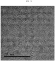
- FIG. 7 is a High Resolution-Transmission Electron Microscope (HR-TEM) image of a MoS 2 thin film manufactured according to a method of manufacturing transition metal chalcogenide thin films according to Example 1 of the present disclosure.
- HR-TEM High Resolution-Transmission Electron Microscope
- FIG. 8 is Raman spectra of a MoS 2 precursor and a MoS 2 thin film manufactured according to a method of manufacturing transition metal chalcogenide thin films according to Example 1 of the present disclosure.
- FIG. 9 is an HR-TEM image of a MoS 2 thin film manufactured according to a method of manufacturing transition metal chalcogenide thin films according to Example 2 of the present disclosure.
- FIG. 10 is a Raman spectrum of a MoS 2 thin film manufactured according to a method of manufacturing transition metal chalcogenide thin films according to Example 2 of the present disclosure.
- FIG. 11 is an HR-TEM image of an SnS x thin film manufactured according to a method of manufacturing transition metal chalcogenide thin films according to Example 3 of the present disclosure.
- FIG. 12 is a Raman spectrum of an SnS x thin film manufactured according to a method of manufacturing transition metal chalcogenide thin films according to Example 3 of the present disclosure.
- FIG. 13 is an HR-TEM image of an SnS x thin film manufactured according to a method of manufacturing transition metal chalcogenide thin films according to Example 4 of the present disclosure.
- FIG. 14 is a Raman spectrum of an SnS x thin film manufactured according to a method of manufacturing transition metal chalcogenide thin films according to Example 4 of the present disclosure.
- FIG. 15 is an HR-TEM image of a SnSe x thin film manufactured according to a method of manufacturing transition metal chalcogenide thin films according to Example 5 of the present disclosure.
- FIG. 16 is a Raman spectrum of a SnSe x thin film manufactured according to a method of manufacturing transition metal chalcogenide thin films according to Example 5 of the present disclosure.
- FIG. 17 is an HR-TEM image of an InSe x thin film manufactured according to a method of manufacturing transition metal chalcogenide thin films according to Example 6 of the present disclosure.
- FIG. 18 is an electron diffraction pattern for an HR-TEM image area of FIG. 17 .
- FIG. 19 is an Energy-dispersive X-ray spectroscopy (EDS) spectrum for the HR-TEM image area of FIG. 17 , and an elemental composition obtained therethrough.
- EDS Energy-dispersive X-ray spectroscopy
- FIG. 20 is a Raman spectrum of an InSe x thin film manufactured according to a method of manufacturing transition metal chalcogenide thin films according to Example 6 of the present disclosure.
- FIG. 21 is an HR-TEM image of an InSe x thin film manufactured according to a method of manufacturing transition metal chalcogenide thin films according to Example 7 of the present disclosure.
- FIG. 22 is an EDS spectrum for an HR-TEM image area of FIG. 21 , and an elemental composition obtained therethrough.
- FIG. 23 is an HR-TEM image of an InSe x thin film manufactured according to a method of manufacturing transition metal chalcogenide thin films according to Example 8 of the present disclosure.
- FIG. 24 is a Raman spectrum of an InSe x thin film manufactured according to a method of manufacturing transition metal chalcogenide thin films according to Example 8 of the present disclosure.
- FIG. 25 is an HR-TEM image of an SnS x thin film manufactured according to a method of manufacturing transition metal chalcogenide thin films according to Comparative Example 1 of the present disclosure.
- FIG. 26 is a high magnification HR-TEM image of an SnS x thin film manufactured according to a method of manufacturing transition metal chalcogenide thin films according to Comparative Example 1 of the present disclosure.
- first,” “second,” and “third” may be used herein to describe various members, components, regions, layers, or sections, these members, components, regions, layers, or sections are not to be limited by these terms. Rather, these terms are only used to distinguish one member, component, region, layer, or section from another member, component, region, layer, or section. Thus, a first member, component, region, layer, or section referred to in examples described herein may also be referred to as a second member, component, region, layer, or section without departing from the teachings of the examples.
- spatially relative terms such as “above,” “upper,” “below,” and “lower” may be used herein for ease of description to describe one element's relationship to another element as shown in the figures. Such spatially relative terms are intended to encompass different orientations of the device in use or operation in addition to the orientation depicted in the figures. For example, if the device in the figures is turned over, an element described as being “above” or “upper” relative to another element will then be “below” or “lower” relative to the other element. Thus, the term “above” encompasses both the above and below orientations depending on the spatial orientation of the device.
- the device may also be oriented in other ways (for example, rotated 90 degrees or at other orientations), and the spatially relative terms used herein are to be interpreted accordingly.
- a term of “a combination thereof” included in a Markush type expression which means a mixture or combination of one or more selected from the group consisting of elements described in the Markush type expression, and means including one or more selected from the group consisting of the elements.
- transition metal chalcogenide thin films according to the present disclosure will be described in detail with reference to embodiments, examples and drawings. However, the present disclosure is not limited to such embodiments, examples and drawings.
- a first aspect of the present disclosure provides a method of manufacturing transition metal chalcogenide thin films, the manufacturing method including the operations of: forming a transition metal chalcogenides precursor on a substrate; and irradiating light onto the transition metal chalcogenides precursor, in which the transition metal chalcogenides precursor includes an amine-based ligand.
- a method of manufacturing chalcogenide thin films according to the present disclosure enables the formation of transition metal chalcogenide thin films in a room temperature range, for example, in a low temperatures range of 20° C. to 40° C. Since deformation of a plastic flexible substrate does not occur in such a temperature range, the transition metal chalcogenide thin films may be directly formed on the plastic flexible substrate. Accordingly, a transfer process which may leave cracks, residues or the like is also unnecessary.
- transition metal chalcogenide thin films As a method of manufacturing transition metal chalcogenide thin films according to the present disclosure enables a process operation to be carried out at low temperatures as described above, various substrates may be selected and used depending on the purpose regardless of thermal properties such as thermal expansion coefficient, heat resistance, etc. of the substrate.
- transition metal chalcogenide thin films may be directly formed on the substrate requiring low processing temperatures.
- a method of manufacturing transition metal chalcogenide thin films according to the present disclosure has excellent reactivity to light by using a precursor including an amine-based ligand. Further, a method of manufacturing transition metal chalcogenide thin films according to the present disclosure may enable very high crystallinity to be implemented compared to the level normally expected at low temperatures by the transition metal chalcogenide thin films by facilitating separation of the ligand due to irradiation of light. Further, a method of manufacturing transition metal chalcogenide thin films according to the present disclosure facilitates solubilization of the precursor and uniform application of the precursor on the substrate, making it easy to manufacture the transition metal chalcogenide thin films through large-area formation and continuous process.
- FIG. 1 is a flowchart showing a method of manufacturing transition metal chalcogenide thin films according to an embodiment of the present disclosure.
- a transition metal chalcogenides precursor is formed on a substrate in order to manufacture transition metal chalcogenide thin films (S 100 ).
- the transition metal chalcogenides precursor may be formed by a method selected from the group consisting of spin coating, bar coating, inkjet printing, nozzle printing, spray coating, slot die coating, gravure printing, screen printing, electrohydrodynamic jet printing, electrospray, and combinations thereof, but the present disclosure is not limited thereto.
- the operation of forming the transition metal chalcogenides precursor may include patterning the transition metal chalcogenides precursor to form the transition metal chalcogenides, but the present disclosure is not limited thereto.
- FIG. 2 is a conceptual diagram showing a method of manufacturing chalcogenide thin films according to an embodiment of the present disclosure.
- FIG. 3 is a conceptual diagram showing a method of manufacturing chalcogenide thin films according to an embodiment of the present disclosure.
- the precursor when forming the precursor on the substrate by spin coating or bar coating, the precursor may be uniformly formed on the substrate. Although it will be described later, an additional patterning operation may be carried out in a subsequent process if necessary.
- the transition metal chalcogenides precursor when carrying out an inkjet printing operation, the transition metal chalcogenides precursor is formed on the substrate, and patterns may be formed on the transition metal chalcogenides precursor at the same time. Accordingly, a finally patterned transition metal chalcogenide thin films may be obtained.
- the transition metal chalcogenides precursor may include a material represented by the following chemical formula 1, but the present disclosure is not limited thereto: LMX n+m , [Chemical Formula 1]
- the M is Mo, In, W, Hf, V, Sn, Re, Ta, Zn, Ga, Ge, Mn, As, Sb, Bi or Ti
- the L is an amine-based ligand coordinated to the M
- the X is S, Se or Te
- the n is more than 0 to not more than 4
- the m is more than 0 to not more than 12.
- the n in chemical formula 1 of the transition metal chalcogenides precursor may mean the number of chalcogen atoms bonded to one atom of a transition metal included in transition metal chalcogenide thin films manufactured by the chalcogenides precursor, and the n+m may mean the number of chalcogen atoms bonded to one atom of the transition metal, which are capable of stabilizing the transition metal chalcogenides precursor.
- the transition metal chalcogenide thin films may include a material represented by the following chemical formula 2, but the present disclosure is not limited thereto: MX n , [Chemical Formula 2]
- the M is Mo, In, W, Hf, V, Sn, Re, Ta, Zn, Ga, Ge, Mn, As, Sb, Bi or Ti
- the X is S, Se or Te
- the n is more than 0 to not more than 4.
- the transition metal chalcogenides precursor may be formed in a form in which an amine-based ligand and an additional chalcogen element are bonded onto a transition metal chalcogenides.
- the transition metal chalcogenides precursor may have a higher proportion of the chalcogen element to the transition metal compared to the transition metal chalcogenides that is synthesized.
- transition metal chalcogenides precursor and/or the transition metal chalcogenide thin films may include one type of transition metal element (M) and chalcogen element (X) respectively, it is also possible that the transition metal chalcogenides precursor and/or the transition metal chalcogenide thin films may include two or more types of transition metal element (M) and chalcogen element (X) respectively.
- the amine-based ligand may be selected from the group consisting of NH 4 + , N 2 H 5 + , CH 3 NH 3 + , hydrazine, ethylenediamine, 2-aminoethanol, and combinations thereof, but the present disclosure is not limited thereto.
- the ligand may be one type of amine-based ligand, or a combination of two or more types of ligand, including the one type of amine-based ligand.
- Transition metal chalcogenide thin films manufactured according to the method of manufacturing the present disclosure depending on the types and molecular weights of the ligand may have different uniformities and crystallinities.
- a wavelength required for crystallization of the transition metal chalcogenide thin films may be shortened.
- High crystallinity means that a crystal close to a single crystal is formed.
- light with a shorter wavelength may be required to obtain a high crystalline transition metal chalcogenide thin films when using CH 3 NH 3 + or N 2 H 5 + as the amine-based ligand compared to when using NH 4 + as the amine-based ligand.
- a method of manufacturing transition metal chalcogenide thin films according to the present disclosure has excellent reactivity to light by using a precursor including an amine-based ligand. Further, a method of manufacturing transition metal chalcogenide thin films according to the present disclosure may enable very high crystallinity to be implemented compared to the level normally expected at low temperatures by the transition metal chalcogenide thin films by facilitating separation of the ligand due to irradiation of light. Further, a method of manufacturing transition metal chalcogenide thin films according to the present disclosure facilitates solubilization of the precursor and uniform application of the precursor on the substrate, making it easy to manufacture the transition metal chalcogenide thin films through large-area formation and continuous process.
- the operation of forming the transition metal chalcogenides precursor may be performed by applying a solution of the transition metal chalcogenides precursor onto the substrate, but the present disclosure is not limited thereto.
- the solution may be selected from the group consisting of ethylenediamine, 2-aminoethanol, dimethyl sulfoxide, dimethylformamide, N-methyl-2-pyrrolidone, 1,2-ethanedithiol, ethylene glycol, ether, DMF, THF, HMPA, and combinations thereof, but the present disclosure is not limited thereto.
- the solution may be replaced with a ligand coordinated on the transition metal chalcogenides precursor by containing a material that may act as a ligand for the transition metal chalcogenides precursor.
- the transition metal chalcogenides precursor may include a transition metal chalcogenides precursor obtained by dissolving a commercially available transition metal chalcogenides precursor in a solvent, or a transition metal chalcogenides precursor formed in the form of a solution.
- the operation of irradiating light may be performed under a temperature of 20° C. to 40° C., but the present disclosure is not limited thereto.
- a method of manufacturing chalcogenide thin films according to the present disclosure enables transition metal chalcogenide thin films to be formed in the foregoing low-temperature range. As deformation of a plastic flexible substrate does not occur in such a temperature range, the transition metal chalcogenide thin films may be directly formed on the plastic flexible substrate. Therefore, a transfer process that may leave cracks, residues, and the like is also unnecessary.
- the substrate may be selected from the group consisting of a polymer including polyethylene naphthalate, polyphenyl sulfide, cyclic olefin copolymer, polyetherimide, polyarylate, polyimide, polyethylene terephthalate, nanocellulose, polydimethylsiloxane, polyamide, polycarbonate, polynorbornene, polyacrylate, polyvinyl alcohol, polyethersulfone, polystyrene, polypropylene, polyethylene, polybutylene terephthalate, polymethacrylate or combinations thereof, a ceramic including SiO 2 , Al 2 O 3 , ZrO 2 , Si 3 N 4 , SiC, AlN, Fe 2 O 3 , ZnO, BN or combinations thereof, and combinations thereof, but the present disclosure is not limited thereto.
- a polymer including polyethylene naphthalate, polyphenyl sulfide, cyclic olefin copolymer, polyetherimide, polyary
- transition metal chalcogenide thin films As a method of manufacturing transition metal chalcogenide thin films according to the present disclosure enables a process operation to be carried out at low temperatures as described above, various substrates may be selected and used depending on the purpose regardless of thermal properties such as thermal expansion coefficient, heat resistance, etc. of the substrate.
- transition metal chalcogenide thin films may be directly formed on the substrate requiring low processing temperatures. Therefore, the transition metal chalcogenide thin films may be directly formed on the flexible substrates without performing the transfer process.
- a method of manufacturing transition metal chalcogenide thin films according to the present disclosure may include irradiating the light onto the transition metal chalcogenides precursor to decompose a portion of the transition metal chalcogenides precursor formed on the substrate so that the transition metal chalcogenide thin films is formed on the substrate.
- the light may include light having a wavelength region of 180 nm to 500 nm, but the present disclosure is not limited thereto.
- the light may include light having a wavelength region of 180 nm to 500 nm.
- the light having the wavelength region includes ultraviolet rays (UV-A, UV-B, and UV-C) and visible lights having short wavelengths (violet, blue and green regions).
- ultraviolet rays UV-A, UV-B, and UV-C
- visible lights having short wavelengths violet, blue and green regions.
- FIGS. 4 to 6 are graphs showing wavelength regions of lights used in a method of manufacturing transition metal chalcogenide thin films according to an example of the present disclosure.
- transition metal chalcogenide thin films manufactured according to wavelengths of lights irradiated may have different uniformities and crystallinities.
- Transition metal chalcogenide thin films may have different optimal light wavelengths required for crystallization depending on a metal element forming the transition metal chalcogenide thin films.
- Transition metal chalcogenide thin films including a metal element having a low melting point, may have a relatively long wavelength required to secure high crystallinity.
- a highly crystalline transition metal chalcogenide thin films may be obtained in a relatively long wavelength region when using In as the metal element compared to when using Mo as the metal element.
- a method of manufacturing transition metal chalcogenide thin films according to the present disclosure may adjust the ratio of chalcogen element to the metal element.
- a method of manufacturing transition metal chalcogenide thin films according to the present disclosure may manufacture transition metal chalcogenide thin films having a high ratio of the chalcogen element to the metal element by irradiating light having a relatively long wavelength.
- a method of manufacturing transition metal chalcogenide thin films according to the present disclosure may manufacture transition metal chalcogenide thin films with different composition ratios depending on the irradiation time of light. For example, when irradiating the light for a long time, transition metal chalcogenide thin films with more excellent crystallinity and a large domain size may be obtained.
- the irradiation time of the light for obtaining transition metal chalcogenide thin films with excellent crystallinity may vary depending on the wavelength of the light. For example, when irradiating light with a short wavelength (with large energy), the irradiation time of light for obtaining transition metal chalcogenide thin films with excellent crystallinity may be reduced.
- a method of manufacturing transition metal chalcogenide thin films according to the present disclosure when irradiating the light, may form a pattern using a photomask.
- a second aspect of the present disclosure provides the transition metal chalcogenide thin films manufactured by the method according to the first aspect of the present disclosure.
- transition metal chalcogenide thin films are directly formed on a flexible substrate so that the transition metal chalcogenide thin films may be used in a flexible device without performing a separate transfer process.
- a transition metal chalcogenides precursor solution was formed by dissolving 11.0 mg of commercially available (NH 4 ) 2 MoS 4 in 1.00 ml of dimethylformamide (DMF). After spin-coating the solution on a SiO 2 /Si substrate in a low-humidity environment, the solution spin-coated on the substrate was dried to form a precursor layer on the substrate. Thereafter, MoS 2 transition metal chalcogenide thin films were finally formed on the substrate by irradiating UV-C onto the precursor layer using a Sankyo UV-C G8T5 8 W lamp at a temperature of about 25° C., thereby decomposing a portion of the precursor.
- DMF dimethylformamide
- FIG. 7 is an HR-TEM image of a MoS 2 thin film manufactured according to a method of manufacturing transition metal chalcogenide thin films according to Example 1 of the present disclosure.
- transition metal chalcogenide thin films with excellent crystallinity and large-sized crystal domain is manufactured.
- FIG. 8 is Raman spectra of a MoS 2 precursor and a MoS 2 thin film manufactured according to a method of manufacturing transition metal chalcogenide thin films according to Example 1 of the present disclosure.
- transition metal chalcogenides may be formed.
- a transition metal chalcogenides precursor solution was formed by dissolving 11.0 mg of commercially available (NH 4 ) 2 MoS 4 in 1.00 ml of dimethylformamide (DMF). After spin-coating the solution on a SiO 2 /Si substrate in a low-humidity environment, the solution spin-coated on the substrate was dried to form a precursor layer on the substrate. Thereafter, MoS 2 transition metal chalcogenide thin films were finally formed on the substrate by irradiating UV-A onto the precursor layer using a Hitachi F8T5 8 W lamp at a temperature of about 25° C., thereby decomposing a portion of the precursor.
- DMF dimethylformamide
- FIG. 9 is an HR-TEM image of a MoS 2 thin film manufactured according to a method of manufacturing transition metal chalcogenide thin films according to Example 2 of the present disclosure.
- transition metal chalcogenide thin films with excellent crystallinity and large-sized crystal domain are manufactured.
- FIG. 10 is a Raman spectrum of a MoS 2 thin film manufactured according to a method of manufacturing transition metal chalcogenide thin films according to Example 2 of the present disclosure.
- transition metal chalcogenides may be formed.
- UV-C and UV-A may exhibit the same effect when forming transition metal chalcogenides using the precursor.
- light decomposing the precursor to form a specific transition metal chalcogenides may not be a single wavelength.
- a transition metal chalcogenides precursor solution was prepared by dissolving 19.5 mg of commercially available tin (II) sulfide (SnS) and 32.6 mg of commercially available sulfur (S) in 1.50 ml of anhydrous hydrazine prepared by dehydration of hydrazine hydrate. After spin-coating the solution on a SiO 2 /Si substrate in a low-humidity environment, the solution spin-coated on the substrate was dried to form a precursor layer on the substrate.
- transition metal chalcogenide thin films were finally formed on the substrate by irradiating UV-C onto the precursor layer at a distance of 20 cm using a Sankyo UV-C G8T5 8 W lamp at a temperature of about 25° C. for one hour, thereby decomposing a portion of the precursor.
- FIG. 11 is an HR-TEM image of the thin film manufactured according to a method of manufacturing transition metal chalcogenide thin films according to Example 3 of the present disclosure.
- FIG. 12 is a Raman spectrum of an SnS x thin film manufactured according to a method of manufacturing transition metal chalcogenide thin films according to Example 3 of the present disclosure.
- the formed crystal is SnS 2 .
- An SnS x thin film was manufactured in the same manner as Example 3 except that UV-C was irradiated for 12 hours, i.e., a long time compared to Example 3.
- FIG. 13 is an HR-TEM image of an SnS x thin film manufactured according to a method of manufacturing transition metal chalcogenide thin films according to Example 4 of the present disclosure.
- transition metal chalcogenide thin films having excellent crystallinity and large-sized crystal domain was manufactured, and a more excellent crystal was obtained compared to FIG. 11 according to Example 3.
- FIG. 14 is a Raman spectrum of an SnS x thin film manufactured according to a method of manufacturing transition metal chalcogenide thin films according to Example 4 of the present disclosure.
- Example 4 a thin film finally formed according to Example 4 is mainly included of SnS differently from Example 3. Further, when comparing FIG. 14 with FIG. 12 of Example 3, it can be confirmed that material with a different composition ratio may be obtained depending on irradiation time when using light with the same wavelength as the same precursor.
- a transition metal chalcogenides precursor solution was prepared by dissolving 24.7 mg of commercially available SnSe and 29.6 mg of commercially available Se in 1.50 ml of anhydrous hydrazine prepared by dehydration of hydrazine hydrate. After spin-coating the solution on a SiO 2 /Si substrate in a low-humidity environment, the solution spin-coated on the substrate was dried to form a precursor layer on the substrate.
- FIG. 15 is an HR-TEM image of a SnSe x thin film manufactured according to a method of manufacturing transition metal chalcogenide thin films according to Example 5 of the present disclosure.
- transition metal chalcogenide thin films with excellent crystallinity and large-sized crystal domain are manufactured.
- FIG. 16 is a Raman spectrum of a SnSe x thin film manufactured according to a method of manufacturing transition metal chalcogenide thin films according to Example 5 of the present disclosure.
- Example 5 a thin film formed according to Example 5 is mainly included in SnSe 2 .
- a transition metal chalcogenides precursor solution was prepared by dissolving 57.5 mg of commercially available In 2 Se 3 and 12.7 mg of commercially available Se in 1.50 ml of anhydrous hydrazine prepared by dehydration of hydrazine hydrate. After spin-coating the solution on a SiO 2 /Si substrate in a low-humidity environment, the solution spin-coated on the substrate was dried to form a precursor layer on the substrate. Thereafter, an InSe x (1 ⁇ x ⁇ 3) transition metal chalcogenide thin films was finally formed on the substrate by irradiating UV-A onto the precursor layer using a Hitachi F8T5 8 W lamp at a temperature of about 25° C., thereby decomposing a portion of the precursor.
- FIG. 17 is an HR-TEM image of an InSe x thin film manufactured according to a method of manufacturing transition metal chalcogenide thin films according to Example 6 of the present disclosure.
- transition metal chalcogenide thin films with excellent crystallinity is manufactured.
- FIG. 18 is an electron diffraction pattern for an HR-TEM image area of FIG. 17 .
- crystal domains with a single crystal structure are mainly oriented in a random direction.
- FIG. 19 is an EDS spectrum for the HR-TEM image area of FIG. 17 , and an elemental composition obtained therethrough.
- elements composing the thin film manufactured according to a method of manufacturing transition metal chalcogenide thin films according to Example 6 of the present disclosure are indium (In) and selenium (Se).
- FIG. 20 is a Raman spectrum of an InSe x thin film manufactured according to a method of manufacturing transition metal chalcogenide thin films according to Example 6 of the present disclosure.
- the formed thin film is mainly included in In 2 Se 3 .
- a transition metal chalcogenides precursor solution was prepared by dissolving 57.5 mg of commercially available In 2 Se 3 and 12.7 mg of commercially available Se in 1.50 ml of anhydrous hydrazine prepared by dehydration of hydrazine hydrate. After spin-coating the solution on a SiO 2 /Si substrate in a low-humidity environment, the solution spin-coated on the substrate was dried to form a precursor layer on the substrate.
- an InSe x (1 ⁇ x ⁇ 3) transition metal chalcogenide thin films was finally formed on the substrate by irradiating UV-C onto the precursor layer using a Sankyo UV-C G8T5 8 W lamp at a temperature of about 25° C., thereby decomposing a portion of the precursor.
- FIG. 21 is an HR-TEM image of a portion of an InSe x thin film manufactured according to a method of manufacturing transition metal chalcogenide thin films according to Example 7 of the present disclosure.
- FIG. 22 is an EDS spectrum for an HR-TEM image area of FIG. 21 , and an elemental composition obtained therethrough.
- a main element composing the thin film of the HR-TEM image area of FIG. 21 is selenium (Se), and it can be confirmed that an amorphous selenium (Se) film is formed without forming InSe x on some areas when irradiating UV-C therethrough.
- wavelengths of light irradiated onto the precursors affect uniformity and crystallinity of the thin films.
- a solution was prepared by dissolving 59.2 mg of commercially available In 2 Se 3 and 10.1 mg of commercially available Se in 1.50 ml of anhydrous hydrazine prepared by dehydration of hydrazine hydrate. After adding 600 ⁇ L of 2-aminoethanol/DMSO with a 3:5 v/v ratio to 150 ⁇ L of the solution to obtain a mixed solution, the mixed solution was heated until a precipitate was formed at 160° C. Thereafter, a centrifugal process was performed to separate the precipitate.
- a transition metal chalcogenides precursor solution was prepared by adding 150 ⁇ L of a 2-aminoethanol/DMSO solvent with a 3:5 v/v ratio to the separated precipitate.
- the solution spin-coated on the substrate was dried to form a precursor layer on the substrate.
- an InSe x (1 ⁇ x ⁇ 3) transition metal chalcogenide thin films was finally formed on the substrate by irradiating UV-C onto the precursor layer using a Sankyo UV-C G8T5 8 W lamp, thereby decomposing a portion of the precursor.
- FIG. 23 is an HR-TEM image of an InSe x thin film manufactured according to a method of manufacturing transition metal chalcogenide thin films according to Example 8 of the present disclosure.
- FIG. 24 is a Raman spectrum of an InSe x thin film manufactured according to a method of manufacturing transition metal chalcogenide thin films according to Example 8 of the present disclosure.
- transition metal chalcogenide thin films manufactured using a transition metal chalcogenides precursor including a ligand with a large molecular weight is formed in the form of amorphous In 2 Se 3 .
- a transition metal chalcogenides precursor solution was prepared by dissolving 19.5 mg of commercially available SnS and 32.6 mg of commercially available sulfur (S) in 1.50 ml of anhydrous hydrazine prepared by dehydration of hydrazine hydrate. After spin-coating the solution on a SiO 2 /Si substrate in a low-humidity environment, the solution spin-coated on the substrate was dried to form a precursor layer on the substrate. Thereafter, an SnS x (1 ⁇ x ⁇ 3) transition metal chalcogenide thin films was finally formed on the substrate by heat-treating the precursor layer to a temperature of 300° C.
- FIG. 25 is an HR-TEM image of an SnS x thin film manufactured according to a method of manufacturing transition metal chalcogenide thin films according to Comparative Example 1 of the present disclosure.
- FIG. 26 is an HR-TEM image having a high magnification compared to FIG. 25 of an SnS x thin film manufactured according to a method of manufacturing transition metal chalcogenide thin films according to Comparative Example 1 of the present disclosure.
- transition metal chalcogenide thin films with more excellent crystallinity may be manufactured by performing the ultraviolet light-irradiating process at room temperature instead of performing the heat treatment process at high temperatures.
Landscapes
- Chemical & Material Sciences (AREA)
- Materials Engineering (AREA)
- Metallurgy (AREA)
- General Chemical & Material Sciences (AREA)
- Chemical Kinetics & Catalysis (AREA)
- Engineering & Computer Science (AREA)
- Organic Chemistry (AREA)
- Mechanical Engineering (AREA)
- Thermal Sciences (AREA)
- Physics & Mathematics (AREA)
- Inorganic Chemistry (AREA)
- Health & Medical Sciences (AREA)
- Toxicology (AREA)
- Inorganic Compounds Of Heavy Metals (AREA)
- Semiconductor Memories (AREA)
Abstract
Description
- MXn, where, the M is Mo, In, W, Hf, V, Sn, Re, Ta, Zn, Ga, Ge, Mn, As, Sb, Bi or Ti, the X is S, Se or Te, and the n is greater than 0 but less than or equal to 4.
LMXn+m, [Chemical Formula 1]
MXn, [Chemical Formula 2]
Claims (15)
Applications Claiming Priority (2)
| Application Number | Priority Date | Filing Date | Title |
|---|---|---|---|
| KR1020190162621A KR20210072373A (en) | 2019-12-09 | 2019-12-09 | Transition-metal chalcogenide thin film and preparing method of the same |
| KR10-2019-0162621 | 2019-12-09 |
Publications (2)
| Publication Number | Publication Date |
|---|---|
| US20210172065A1 US20210172065A1 (en) | 2021-06-10 |
| US11753721B2 true US11753721B2 (en) | 2023-09-12 |
Family
ID=76209511
Family Applications (1)
| Application Number | Title | Priority Date | Filing Date |
|---|---|---|---|
| US17/116,053 Active US11753721B2 (en) | 2019-12-09 | 2020-12-09 | Transition-metal chalcogenide thin film and preparing method of the same |
Country Status (2)
| Country | Link |
|---|---|
| US (1) | US11753721B2 (en) |
| KR (2) | KR20210072373A (en) |
Families Citing this family (1)
| Publication number | Priority date | Publication date | Assignee | Title |
|---|---|---|---|---|
| CN119998490A (en) * | 2022-10-07 | 2025-05-13 | 秀博瑞殷株式公社 | Dielectric film activator, semiconductor substrate and semiconductor device manufactured using the same |
Citations (6)
| Publication number | Priority date | Publication date | Assignee | Title |
|---|---|---|---|---|
| US20050009225A1 (en) * | 2003-07-10 | 2005-01-13 | International Business Machines Corporation | Hydrazine-free solution deposition of chalcogenide films |
| US20070166645A1 (en) * | 2005-10-18 | 2007-07-19 | Jeong Hyun D | Chalcogenide precursor compound and method for preparing chalcogenide thin film using the same |
| KR20070080723A (en) | 2006-02-08 | 2007-08-13 | 삼성코닝 주식회사 | Patterning method of chalcogenide thin film |
| US20090191483A1 (en) * | 2008-01-30 | 2009-07-30 | E. I. Du Pont De Nemours And Company | Device and method for preparing relief printing form |
| KR101623791B1 (en) | 2014-05-23 | 2016-05-24 | 엘지전자 주식회사 | Method for manufacturing metal chalcogenide film and the film manufactured by the same |
| KR20190121632A (en) | 2018-04-18 | 2019-10-28 | 한국과학기술연구원 | Large-area, Selective and High-speed Synthesis Method of Transition-Metal Dichalcogenides Using Laser and Transition-Metal Dichalcogenides Prepared Thereby |
-
2019
- 2019-12-09 KR KR1020190162621A patent/KR20210072373A/en not_active Ceased
-
2020
- 2020-12-09 US US17/116,053 patent/US11753721B2/en active Active
-
2021
- 2021-12-28 KR KR1020210190079A patent/KR102498280B1/en active Active
Patent Citations (6)
| Publication number | Priority date | Publication date | Assignee | Title |
|---|---|---|---|---|
| US20050009225A1 (en) * | 2003-07-10 | 2005-01-13 | International Business Machines Corporation | Hydrazine-free solution deposition of chalcogenide films |
| US20070166645A1 (en) * | 2005-10-18 | 2007-07-19 | Jeong Hyun D | Chalcogenide precursor compound and method for preparing chalcogenide thin film using the same |
| KR20070080723A (en) | 2006-02-08 | 2007-08-13 | 삼성코닝 주식회사 | Patterning method of chalcogenide thin film |
| US20090191483A1 (en) * | 2008-01-30 | 2009-07-30 | E. I. Du Pont De Nemours And Company | Device and method for preparing relief printing form |
| KR101623791B1 (en) | 2014-05-23 | 2016-05-24 | 엘지전자 주식회사 | Method for manufacturing metal chalcogenide film and the film manufactured by the same |
| KR20190121632A (en) | 2018-04-18 | 2019-10-28 | 한국과학기술연구원 | Large-area, Selective and High-speed Synthesis Method of Transition-Metal Dichalcogenides Using Laser and Transition-Metal Dichalcogenides Prepared Thereby |
Non-Patent Citations (3)
| Title |
|---|
| Korean Office Action dated Jul. 6, 2021 in counterpart Korean Patent Application No. 10-2019-0162621 (4 pages in Korean). |
| Liu et al "Growth of Large-Area and Highly Crystalline MoS2 Thin layers on Insulating substrates" Nano Lett. 2012 12, 1538-1544. (Year: 2012). * |
| Simonds et al "Laser processing for thin film chalcogenide photovoltaics: a review and prospectus" J. Phontonics for Energy, vol. 5 2015, 050999-1-20 (Year: 2015). * |
Also Published As
| Publication number | Publication date |
|---|---|
| KR20210072373A (en) | 2021-06-17 |
| US20210172065A1 (en) | 2021-06-10 |
| KR20220002833A (en) | 2022-01-07 |
| KR102498280B1 (en) | 2023-02-08 |
Similar Documents
| Publication | Publication Date | Title |
|---|---|---|
| Wang et al. | Toward wafer‐scale production of 2D transition metal chalcogenides | |
| JP2012527402A (en) | Method for producing copper tin sulfide and copper zinc tin sulfide films | |
| Sytnyk et al. | Epitaxial metal halide perovskites by inkjet‐printing on various substrates | |
| KR102042680B1 (en) | Large-area, Selective and High-speed Synthesis Method of Transition-Metal Dichalcogenides Using Laser and Transition-Metal Dichalcogenides Prepared Thereby | |
| US11753721B2 (en) | Transition-metal chalcogenide thin film and preparing method of the same | |
| Muydinov et al. | Crystallisation behaviour of CH3NH3PbI3 films: The benefits of sub-second flash lamp annealing | |
| Srivathsa et al. | Ultraviolet photoconductivity and photoluminescence properties of spray pyrolyzed ZnO nanostructure: Effect of deposition temperature | |
| Wang et al. | Selective‐Area Growth of Aligned Organic Semiconductor Nanowires and Their Device Integration | |
| Iacomi et al. | Physical characterization of CdMnS nanocrystalline thin films grown by vacuum thermal evaporation | |
| Li et al. | Halide vapor phase epitaxy of monolayer molybdenum diselenide single crystals | |
| Jamshaid et al. | Synthesis and characterization of BaZrS3 thin films via stacked layer methodology: a comparative study of BaZrS3 on zirconium foil and silicon carbide substrates | |
| El-Menyawy | Optical properties of amorphous and crystalline tris (8-hydroxyquinoline) indium films | |
| US10745289B2 (en) | Vanadium oxide film and process for producing same | |
| Kim et al. | Investigation of crystallized ZnSnO3 nanoparticles for ultraviolet photodetectors | |
| Liao et al. | The effects of solvents on the highly oriented ZnO films prepared using sol–gel method | |
| US11887849B2 (en) | Method of forming transition metal dichalcogenidethin film and method of manufacturing electronic device including the same | |
| Shkir et al. | Structural, Elemental, Morphological and Optical Spectroscopic Studies on High Quality〈 111〉 Grown Nanocrystalline ZnTe Thin Films: An Effect of Thickness | |
| Buono-Core et al. | Characterization of pure ZnO thin films prepared by a direct photochemical method | |
| Wong | Chemical vapor deposition growth of 2D semiconductors | |
| Balderas et al. | Antisolvent‐Enhanced Crystallization of Luminescent All‐Green Organic–Inorganic Manganese‐Halide Films Deposited by Aerosol‐Assisted Chemical Vapor Deposition Technique on Either Glass or Elastomer Substrates | |
| Lin et al. | Electrical and ferromagnetic properties of p-type ZnO thin films with and without the addition of graphene prepared by the sol-gel method | |
| Alcaire et al. | Highly Porous ZnO Thin Films and 1D Nanostructures by Remote Plasma Processing of Zn‐Phthalocyanine | |
| KR102275058B1 (en) | Method for manufacturing patterned perovskite films and apparatus using the same | |
| EP2778263B1 (en) | Low temperature, thin film crystallization method and products prepared therefrom | |
| US8288767B2 (en) | Thin-film transistor and forming method thereof |
Legal Events
| Date | Code | Title | Description |
|---|---|---|---|
| AS | Assignment |
Owner name: RESEARCH & BUSINESS FOUNDATION SUNGKYUNKWAN UNIVERSITY, KOREA, REPUBLIC OF Free format text: ASSIGNMENT OF ASSIGNORS INTEREST;ASSIGNORS:LEE, CHANGGU;YOO, HYONGGOO;REEL/FRAME:054590/0629 Effective date: 20201204 |
|
| FEPP | Fee payment procedure |
Free format text: ENTITY STATUS SET TO UNDISCOUNTED (ORIGINAL EVENT CODE: BIG.); ENTITY STATUS OF PATENT OWNER: SMALL ENTITY |
|
| FEPP | Fee payment procedure |
Free format text: ENTITY STATUS SET TO SMALL (ORIGINAL EVENT CODE: SMAL); ENTITY STATUS OF PATENT OWNER: SMALL ENTITY |
|
| STPP | Information on status: patent application and granting procedure in general |
Free format text: DOCKETED NEW CASE - READY FOR EXAMINATION |
|
| STPP | Information on status: patent application and granting procedure in general |
Free format text: NON FINAL ACTION MAILED |
|
| STPP | Information on status: patent application and granting procedure in general |
Free format text: RESPONSE TO NON-FINAL OFFICE ACTION ENTERED AND FORWARDED TO EXAMINER |
|
| STPP | Information on status: patent application and granting procedure in general |
Free format text: FINAL REJECTION MAILED |
|
| STPP | Information on status: patent application and granting procedure in general |
Free format text: ADVISORY ACTION MAILED |
|
| STPP | Information on status: patent application and granting procedure in general |
Free format text: DOCKETED NEW CASE - READY FOR EXAMINATION |
|
| STPP | Information on status: patent application and granting procedure in general |
Free format text: NON FINAL ACTION MAILED |
|
| STPP | Information on status: patent application and granting procedure in general |
Free format text: AWAITING TC RESP., ISSUE FEE NOT PAID |
|
| STPP | Information on status: patent application and granting procedure in general |
Free format text: PUBLICATIONS -- ISSUE FEE PAYMENT RECEIVED |
|
| STPP | Information on status: patent application and granting procedure in general |
Free format text: PUBLICATIONS -- ISSUE FEE PAYMENT VERIFIED |
|
| STCF | Information on status: patent grant |
Free format text: PATENTED CASE |