US11749735B2 - Method for forming shielding polysilicon sidewall for protecting shielded gate trench metal-oxide-semiconductor field effect transistor - Google Patents
Method for forming shielding polysilicon sidewall for protecting shielded gate trench metal-oxide-semiconductor field effect transistor Download PDFInfo
- Publication number
- US11749735B2 US11749735B2 US17/146,348 US202117146348A US11749735B2 US 11749735 B2 US11749735 B2 US 11749735B2 US 202117146348 A US202117146348 A US 202117146348A US 11749735 B2 US11749735 B2 US 11749735B2
- Authority
- US
- United States
- Prior art keywords
- polysilicon
- layer
- forming
- shielding polysilicon
- oxide layer
- Prior art date
- Legal status (The legal status is an assumption and is not a legal conclusion. Google has not performed a legal analysis and makes no representation as to the accuracy of the status listed.)
- Active, expires
Links
Images


Classifications
-
- H01L29/4236—
-
- H—ELECTRICITY
- H10—SEMICONDUCTOR DEVICES; ELECTRIC SOLID-STATE DEVICES NOT OTHERWISE PROVIDED FOR
- H10D—INORGANIC ELECTRIC SEMICONDUCTOR DEVICES
- H10D64/00—Electrodes of devices having potential barriers
- H10D64/20—Electrodes characterised by their shapes, relative sizes or dispositions
- H10D64/27—Electrodes not carrying the current to be rectified, amplified, oscillated or switched, e.g. gates
- H10D64/311—Gate electrodes for field-effect devices
- H10D64/411—Gate electrodes for field-effect devices for FETs
- H10D64/511—Gate electrodes for field-effect devices for FETs for IGFETs
- H10D64/512—Disposition of the gate electrodes, e.g. buried gates
- H10D64/513—Disposition of the gate electrodes, e.g. buried gates within recesses in the substrate, e.g. trench gates, groove gates or buried gates
-
- H01L29/0623—
-
- H01L29/1083—
-
- H01L29/66734—
-
- H01L29/7813—
-
- H—ELECTRICITY
- H10—SEMICONDUCTOR DEVICES; ELECTRIC SOLID-STATE DEVICES NOT OTHERWISE PROVIDED FOR
- H10D—INORGANIC ELECTRIC SEMICONDUCTOR DEVICES
- H10D30/00—Field-effect transistors [FET]
- H10D30/01—Manufacture or treatment
- H10D30/021—Manufacture or treatment of FETs having insulated gates [IGFET]
- H10D30/028—Manufacture or treatment of FETs having insulated gates [IGFET] of double-diffused metal oxide semiconductor [DMOS] FETs
- H10D30/0291—Manufacture or treatment of FETs having insulated gates [IGFET] of double-diffused metal oxide semiconductor [DMOS] FETs of vertical DMOS [VDMOS] FETs
- H10D30/0297—Manufacture or treatment of FETs having insulated gates [IGFET] of double-diffused metal oxide semiconductor [DMOS] FETs of vertical DMOS [VDMOS] FETs using recessing of the gate electrodes, e.g. to form trench gate electrodes
-
- H—ELECTRICITY
- H10—SEMICONDUCTOR DEVICES; ELECTRIC SOLID-STATE DEVICES NOT OTHERWISE PROVIDED FOR
- H10D—INORGANIC ELECTRIC SEMICONDUCTOR DEVICES
- H10D30/00—Field-effect transistors [FET]
- H10D30/60—Insulated-gate field-effect transistors [IGFET]
- H10D30/64—Double-diffused metal-oxide semiconductor [DMOS] FETs
- H10D30/66—Vertical DMOS [VDMOS] FETs
- H10D30/668—Vertical DMOS [VDMOS] FETs having trench gate electrodes, e.g. UMOS transistors
-
- H—ELECTRICITY
- H10—SEMICONDUCTOR DEVICES; ELECTRIC SOLID-STATE DEVICES NOT OTHERWISE PROVIDED FOR
- H10D—INORGANIC ELECTRIC SEMICONDUCTOR DEVICES
- H10D62/00—Semiconductor bodies, or regions thereof, of devices having potential barriers
- H10D62/10—Shapes, relative sizes or dispositions of the regions of the semiconductor bodies; Shapes of the semiconductor bodies
- H10D62/102—Constructional design considerations for preventing surface leakage or controlling electric field concentration
- H10D62/103—Constructional design considerations for preventing surface leakage or controlling electric field concentration for increasing or controlling the breakdown voltage of reverse-biased devices
- H10D62/105—Constructional design considerations for preventing surface leakage or controlling electric field concentration for increasing or controlling the breakdown voltage of reverse-biased devices by having particular doping profiles, shapes or arrangements of PN junctions; by having supplementary regions, e.g. junction termination extension [JTE]
- H10D62/106—Constructional design considerations for preventing surface leakage or controlling electric field concentration for increasing or controlling the breakdown voltage of reverse-biased devices by having particular doping profiles, shapes or arrangements of PN junctions; by having supplementary regions, e.g. junction termination extension [JTE] having supplementary regions doped oppositely to or in rectifying contact with regions of the semiconductor bodies, e.g. guard rings with PN or Schottky junctions
- H10D62/107—Buried supplementary regions, e.g. buried guard rings
-
- H—ELECTRICITY
- H10—SEMICONDUCTOR DEVICES; ELECTRIC SOLID-STATE DEVICES NOT OTHERWISE PROVIDED FOR
- H10D—INORGANIC ELECTRIC SEMICONDUCTOR DEVICES
- H10D62/00—Semiconductor bodies, or regions thereof, of devices having potential barriers
- H10D62/10—Shapes, relative sizes or dispositions of the regions of the semiconductor bodies; Shapes of the semiconductor bodies
- H10D62/17—Semiconductor regions connected to electrodes not carrying current to be rectified, amplified or switched, e.g. channel regions
- H10D62/351—Substrate regions of field-effect devices
- H10D62/357—Substrate regions of field-effect devices of FETs
- H10D62/364—Substrate regions of field-effect devices of FETs of IGFETs
- H10D62/371—Inactive supplementary semiconductor regions, e.g. for preventing punch-through, improving capacity effect or leakage current
-
- H—ELECTRICITY
- H10—SEMICONDUCTOR DEVICES; ELECTRIC SOLID-STATE DEVICES NOT OTHERWISE PROVIDED FOR
- H10D—INORGANIC ELECTRIC SEMICONDUCTOR DEVICES
- H10D64/00—Electrodes of devices having potential barriers
- H10D64/111—Field plates
- H10D64/117—Recessed field plates, e.g. trench field plates or buried field plates
-
- H—ELECTRICITY
- H10—SEMICONDUCTOR DEVICES; ELECTRIC SOLID-STATE DEVICES NOT OTHERWISE PROVIDED FOR
- H10D—INORGANIC ELECTRIC SEMICONDUCTOR DEVICES
- H10D64/00—Electrodes of devices having potential barriers
- H10D64/20—Electrodes characterised by their shapes, relative sizes or dispositions
- H10D64/27—Electrodes not carrying the current to be rectified, amplified, oscillated or switched, e.g. gates
- H10D64/311—Gate electrodes for field-effect devices
- H10D64/411—Gate electrodes for field-effect devices for FETs
- H10D64/511—Gate electrodes for field-effect devices for FETs for IGFETs
- H10D64/514—Gate electrodes for field-effect devices for FETs for IGFETs characterised by the insulating layers
- H10D64/516—Gate electrodes for field-effect devices for FETs for IGFETs characterised by the insulating layers the thicknesses being non-uniform
-
- H—ELECTRICITY
- H10—SEMICONDUCTOR DEVICES; ELECTRIC SOLID-STATE DEVICES NOT OTHERWISE PROVIDED FOR
- H10D—INORGANIC ELECTRIC SEMICONDUCTOR DEVICES
- H10D30/00—Field-effect transistors [FET]
- H10D30/01—Manufacture or treatment
- H10D30/021—Manufacture or treatment of FETs having insulated gates [IGFET]
- H10D30/028—Manufacture or treatment of FETs having insulated gates [IGFET] of double-diffused metal oxide semiconductor [DMOS] FETs
- H10D30/0291—Manufacture or treatment of FETs having insulated gates [IGFET] of double-diffused metal oxide semiconductor [DMOS] FETs of vertical DMOS [VDMOS] FETs
- H10D30/0295—Manufacture or treatment of FETs having insulated gates [IGFET] of double-diffused metal oxide semiconductor [DMOS] FETs of vertical DMOS [VDMOS] FETs using recessing of the source electrodes
-
- H—ELECTRICITY
- H10—SEMICONDUCTOR DEVICES; ELECTRIC SOLID-STATE DEVICES NOT OTHERWISE PROVIDED FOR
- H10D—INORGANIC ELECTRIC SEMICONDUCTOR DEVICES
- H10D62/00—Semiconductor bodies, or regions thereof, of devices having potential barriers
- H10D62/10—Shapes, relative sizes or dispositions of the regions of the semiconductor bodies; Shapes of the semiconductor bodies
- H10D62/17—Semiconductor regions connected to electrodes not carrying current to be rectified, amplified or switched, e.g. channel regions
- H10D62/393—Body regions of DMOS transistors or IGBTs
-
- H—ELECTRICITY
- H10—SEMICONDUCTOR DEVICES; ELECTRIC SOLID-STATE DEVICES NOT OTHERWISE PROVIDED FOR
- H10D—INORGANIC ELECTRIC SEMICONDUCTOR DEVICES
- H10D64/00—Electrodes of devices having potential barriers
- H10D64/20—Electrodes characterised by their shapes, relative sizes or dispositions
- H10D64/23—Electrodes carrying the current to be rectified, amplified, oscillated or switched, e.g. sources, drains, anodes or cathodes
- H10D64/251—Source or drain electrodes for field-effect devices
- H10D64/252—Source or drain electrodes for field-effect devices for vertical or pseudo-vertical devices
- H10D64/2527—Source or drain electrodes for field-effect devices for vertical or pseudo-vertical devices for vertical devices wherein the source or drain electrodes are recessed in semiconductor bodies
Definitions
- the present invention relates to a method for forming a shielding polysilicon sidewall protection layer for a shielded gate trench metal-oxide-semiconductor field effect transistor (SGT MOSFET).
- SGT MOSFET shielded gate trench metal-oxide-semiconductor field effect transistor
- a gate-to-source leakage current (Igss) from a gate to a source is usually very high and a drain-to-source leakage current (Idss) from a drain to the source also becomes high because a thickness of an oxide in a top region of shielding polysilicon (Poly 1 ) and a thickness of an oxide of a trench sidewall in a transition region between the shielding polysilicon and gate polysilicon become thin.
- the present application provides a method for forming a shielding polysilicon sidewall protection layer for protecting an SGT MOSFET, so as to increase a thickness of an oxide in a top region of shielding polysilicon and a thickness of an oxide of a trench sidewall in a transition region between the shielding polysilicon and gate polysilicon to solve the problem of serious leakage current.
- an oxide layer—silicon-nitrogen compound—oxide layer as a hard mask layer is formed on a semiconductor substrate, and then the trench is etched on the semiconductor substrate from the patterned hard mask layer; the liner oxide layer is grown or deposited in the trench; in situ heavily N-type doped (doping level>2e20/cm 3 ) polysilicon layer is deposited and etched back in the trench; the liner oxide layer is partially removed in the trench; a transition oxide protection layer is grown on the top and sidewall surface of the shielding polysilicon.
- the heavily N-type doped (doping level>2e20/cm 3 ) shielding polysilicon is arranged in the trench, and the heavily N-type doped polysilicon is etched back to retain some materials to form the shielding polysilicon.
- the oxide-nitride hard mask layer, the liner oxide layer and the transition oxide layer on the top surface of the shielding polysilicon are removed by reactive ion dry etching or an HF based wet etching technique.
- thicknesses of the transition oxide layer and the liner oxide layer are the same or different.
- the liner oxide layer for the protective heavily N-type doped shielding polysilicon sidewall is makeable by using a thermal oxidation process or thermal oxidation and a chemical vapor deposition process.
- the IPO layer is composed of a thermal oxide layer or a thermal oxide layer and a chemical vapor deposition oxide layer or a high-density plasma deposition oxide layer or a nitride layer mixed with a thermal oxide layer or a single nitride layer or a low-K dielectric layer.
- the liner oxide layer of the protective shielding polysilicon sidewall is located between the heavily N-type doped shielding polysilicon and the trench sidewall
- the IPO layer of the protected shielding polysilicon sidewall is located between the shielding polysilicon sidewall and the gate polysilicon, including: a first distance and a second distance, wherein the IPO layer further comprises a termination region and a core cell active region.
- a thickness of the IPO layer with the second distance in the termination region is greater than a thickness of the IPO layer with the first distance in the core cell active region.
- the IPO layer is makeable by using the chemical vapor deposition process, and the thickness of the IPO layer with the second distance in the termination region or a thickness of the shielding polysilicon contact to a source metal region is 1000 ⁇ to 3.0 ⁇ m.
- the IPO layer is makeable by using the thermal oxidation process, and the thickness of the IPO layer with the first distance in the core cell active region is 1000 ⁇ to 4000 ⁇ .
- the shielding polysilicon is extensible to the top semiconductor surface of the substrate in the termination trench.
- a thickness of the liner oxide layer in the termination trench is 1000 ⁇ to 3.0 ⁇ m.
- the method further includes: forming a P-type doped body implantation layer and a heavily N-type doped source implantation layer on the surface of the semiconductor substrate; forming an LTO/boron-phosphorosilicate glass (BPSG) oxide layer on a surface of the semiconductor substrate; defining a contact window on a surface of the LTO/BPSG oxide layer; forming a contact on the BPSG oxide layer by removing LTO/BPSG oxide at the contact region, source metal in contact with a source.
- BPSG LTO/boron-phosphorosilicate glass
- P-body implantation may be performed in the termination region.
- the method for forming a shielding polysilicon sidewall for protecting an SGT MOSFET after P-body implantation is performed in the active region, it is necessary to add a trench guard ring to reduce drain-to-source electric leakage.
- a trench guard ring for a MOSFET device with a breakdown voltage less than 80 V, it is unnecessary to add a trench 14 guard ring to reduce drain-to-source electric leakage.
- a MOSFET device with a breakdown voltage greater than 80 V it is necessary to add a trench 14 floating guard ring to reduce drain-to-source electric leakage.
- P-body implantation is not performed in the termination region for a full charge balanced SGT MOSFET, it is unnecessary to add a trench guard ring to reduce drain-to-source electric leakage.
- a breakdown voltage executed on the SGT MOSFET is between 10 V and 300 V.
- FIG. 1 is a schematic diagram of a protected SGT MOSFET structure according to an embodiment of the present application
- FIG. 2 A shows a first step process of a method for forming a shielding polysilicon sidewall for protecting an SGT MOSFET according to an embodiment of the present application
- FIG. 2 B shows a second step process of a method for forming a shielding polysilicon sidewall for protecting an SGT MOSFET according to an embodiment of the present application
- FIG. 2 C shows a third step process of a method for forming a shielding polysilicon sidewall for protecting an SGT MOSFET according to an embodiment of the present application
- FIG. 2 D shows a fourth step process of a method for forming a shielding polysilicon sidewall for protecting an SGT MOSFET according to an embodiment of the present application
- FIG. 2 E shows a fifth step process of a method for forming a shielding polysilicon sidewall for protecting an SGT MOSFET according to an embodiment of the present application
- FIG. 2 F shows a sixth step process of a method for forming a shielding polysilicon sidewall for protecting an SGT MOSFET according to an embodiment of the present application
- FIG. 2 G shows a seventh step process of a method for forming a shielding polysilicon sidewall for protecting an SGT MOSFET according to an embodiment of the present application
- FIG. 3 A shows a first step process of a method for forming a shielding polysilicon sidewall for protecting an SGT MOSFET according to an embodiment of the present application
- FIG. 3 B shows a second step process of a method for forming a shielding polysilicon sidewall for protecting an SGT MOSFET according to an embodiment of the present application
- FIG. 3 C shows a third step process of a method for forming a shielding polysilicon sidewall for protecting an SGT MOSFET according to an embodiment of the present application
- FIG. 3 D shows a fourth step process of a method for forming a shielding polysilicon sidewall for protecting an SGT MOSFET according to an embodiment of the present application
- FIG. 3 E shows a fifth step process of a method for forming a shielding polysilicon sidewall for protecting an SGT MOSFET according to an embodiment of the present application
- FIG. 3 F shows a sixth step process of a method for forming a shielding polysilicon sidewall for protecting an SGT MOSFET according to an embodiment of the present application
- FIG. 3 G shows a seventh step process of a method for forming a shielding polysilicon sidewall for protecting an SGT MOSFET according to an embodiment of the present application
- FIG. 3 H shows an eighth step process of a method for forming a shielding polysilicon sidewall for protecting an SGT MOSFET according to an embodiment of the present application
- FIG. 3 I shows a ninth step process of a method for forming a shielding polysilicon sidewall for protecting an SGT MOSFET according to an embodiment of the present application
- FIG. 3 J is a side view of an IPO layer in a method for forming a shielding polysilicon sidewall for protecting an SGT MOSFET according to an embodiment of the present application;
- FIG. 3 K shows a tenth step process of a method for forming a shielding polysilicon sidewall for protecting an SGT MOSFET according to an embodiment of the present application
- FIG. 3 L shows an eleventh step process of a method for forming a shielding polysilicon sidewall for protecting an SGT MOSFET according to an embodiment of the present application
- FIG. 3 M shows a twelfth step process of a method for forming a shielding polysilicon sidewall for protecting an SGT MOSFET according to an embodiment of the present application.
- FIG. 4 is a schematic diagram of implementation of a protected SGT MOSFET structure according to an embodiment of the present invention.
- 01 shielding polysilicon (Poly 1 ); 02 : gate polysilicon (Poly 2 ); 03 : transition oxide layer; 04 : liner oxide layer; 05 : boron-phosphorosilicate glass (BPSG); 06 : source metal; 07 : semiconductor substrate; 08 a : hard mask layer; 08 b : hard mask layer; 09 : P-body implantation layer; 10 : source implantation layer (N+); 11 : inter poly oxide (IPO) layer; 12 : N-type Epi layer; 13 : N+ substrate; 14 : trench; 15 : P+ contact implantation; 16 : source contact; 17 : first distance (d 1 ); 18 : second distance (d 2 ); 19 : core cell active region; 20 : termination region; 21 : low temperature oxide (LTO)/BPSG oxide layer; 22 : source contact window
- the word “including” shall be understood as including the stated component, but not excluding any other component.
- “on . . . ” means being located above or below a target component, but not having to be located on top based on the gravity direction.
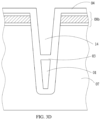
- FIG. 1 is a schematic diagram of an SGT MOSFET structure according to an embodiment of the present application. This embodiment is understood in combination with FIG. 1 .
- Shielding polysilicon 01 is included in a trench 14
- gate polysilicon 02 is located above the shielding polysilicon 01 and spaced from the shielding polysilicon 01 by an IPO layer 11 .
- On a side of the shielding polysilicon 01 there is mainly a liner oxide layer 04 , while above the shielding polysilicon 01 , there is mainly a thermal oxide layer 03 .
- the top of the gate polysilicon 02 is covered by an LTO 21 and a BPSG 05 , and the top and a periphery of the BPSG 05 are covered by metal layer 06 .
- FIG. 2 A to FIG. 2 G are schematic diagrams of step processes of a method for forming a shielding polysilicon sidewall for protecting an SGT MOSFET according to an embodiment of the present application.
- the method includes at least the following steps.
- a hard mask layer 08 a is formed on a heavily N-type doped semiconductor substrate with an N-type epitaxial 07 and the trench 14 is formed on a surface of the semiconductor substrate.
- the hard mask layer 08 a is an oxide layer
- the trench 14 is formed on the surface of the semiconductor substrate by reactive ion plasma dry etching.
- the liner oxide layer 04 is formed on an inner wall of the trench 14 .
- the liner oxide layer 04 may be formed by thermal oxidation or chemical vapor deposition, so that the sidewall of the whole trench 14 and a surface of the hard mask layer 08 a are covered by the liner oxide layer 04 .
- the heavily N-type doped (doping level>2e20 cm 3 ) shielding polysilicon 01 is arranged in the trench 14 .
- a heavily situ doped polysilicon layer is deposited in the trench 14 by chemical vapor deposition to form the shielding polysilicon 01 , and then the shielding polysilicon 01 is etched back, so that the shielding polysilicon 01 from the middle of the trench to the bottom of the trench is retained in the trench, leaving part of space in the trench exposed to air to form an opening.
- a transition oxide layer 03 is formed on a top and sidewall surface of the heavily doped shielding polysilicon 01 .
- the thermal oxide layer 03 may be formed on an upper and sidewall surface of the shielding polysilicon 01 by thermal oxidation or chemical vapor deposition, and is regarded as the transition oxide layer 03 .
- a thickness of the transition oxide layer 03 is the same as or greater than that of the liner oxide layer 04 .
- the hard mask layer 08 a , the liner oxide layer 04 and the transition oxide layer 03 may be removed from a top surface of the shielding polysilicon 01 by etching (dry or wet etching techniques).
- the top of the heavily doped shielding polysilicon 01 may be lower than or flush with the top of the peripheral liner oxide layer 04 .
- the thin transition oxide layer 03 is still retained on the top and sidewall of the heavily doped shielding polysilicon 01 after etching.
- the IPO layer 11 is formed on the top surface of the heavily doped shielding polysilicon 01 , the inner wall of the trench 14 .
- the IPO layer forms a plane, a notch or a protrusion on the top and sidewall surface of the shielding polysilicon 01 due to relative heights of the heavily doped shielding polysilicon 01 and the top of the liner oxide layer 04 and based on whether the transition oxide layer 03 is retained on the top of the shielding polysilicon 01 .
- the IPO layer 11 is composed of a thermal oxide layer or a thermal oxide layer and a chemical vapor deposition oxide layer or a high-density plasma deposition oxide layer or a nitride layer mixed with a thermal oxide layer or a single nitride layer or a low-K dielectric layer.
- the N-type doped gate polysilicon 02 is formed above the heavily N-type doped shielding polysilicon 01 , and the gate polysilicon 02 is isolated from the heavily doped shielding polysilicon 01 through the IPO layer 11 .
- the gate polysilicon 02 is formed by depositing a polysilicon layer in the opening of the trench 14 by chemical vapor deposition, and the top surface of the gate polysilicon 02 is flush with an interface between the semiconductor N-type epitaxial substrate 07 and the hard mask layer 08 a on its surface.
- the heavily N-type doped (doping level>2e20/cm 3 ) shielding polysilicon sidewall is formed due to this heavily N-type doped polysilicon.
- This polysilicon oxidation grown rate is much faster than the lightly doped N-type epitaxial layer and P-type doped body in the mesa between the trenches.
- This thick oxidation layer along the shielding polysilicon sidewall and trench wall forms a protection layer for avoiding gate to source Igss leakage.
- a subsequent transistor forming design and process depend on physical requirements of designers for elements, and no limitation is posed.
- FIG. 3 A to FIG. 3 G are schematic diagrams of step processes of a method for forming a heavily N-type doped (doping level>2e20/cm 3 ) shielding polysilicon sidewall for protecting an SGT MOSFET according to an embodiment of the present application.
- the method includes at least the following steps.
- the trench 14 is etched on the semiconductor N-type epitaxial substrate 07 by taking a three-layer structure of oxide layer—silicon-nitrogen compound—oxide layer as a hard mask layer 08 b on the surface of the semiconductor N-type epitaxial substrate 07 .
- the liner oxide layer 04 is further formed on the sidewall of the trench 14 and a surface of the hard mask layer 08 b by thermal oxidation or chemical vapor deposition, so that the sidewall of the whole trench 14 and the surface of the three-layer structure of the hard mask layer 08 b are both covered by the liner oxide layer 04 .
- a heavily in situ N-type doped (doping level>2e20/cm 3 ) polysilicon layer is deposited in the space in the trench 14 by chemical vapor deposition to form the shielding polysilicon 01 , and then the shielding polysilicon 01 is further etched back to retain a part of the shielding polysilicon 01 in the trench. In this case, only the part of the shielding polysilicon 01 is retained in the trench 14 , leaving part of the space exposed to air to form the opening.
- the transition oxide layer 03 (namely the thermal oxide layer) is formed on the upper and sidewall surface of the shielding polysilicon 01 by thermal oxidation or chemical vapor deposition.
- the shielding polysilicon sidewall with trench is protected, since the oxidation grown rate is much faster for the heavily doped polysilicon layer than that in the lightly doped mesa between trenches.
- This thick shielding polysilicon sidewall oxide layer still partially remain even with later on the liner oxide wet or dry etching process.
- the transition oxide layer 03 is etched on the sidewall of the trench 14 and a silicon surface of the shielding polysilicon 01 to remove the oxide layer on the surface of the semiconductor substrate 07 and retain the silicon-nitrogen compound—oxide layer as the hard mask layer 08 b , the liner oxide layer 04 on the top surface of the shielding polysilicon 01 and the transition oxide layer 03 to form the opening, and the top surface of the shielding polysilicon 01 is higher than the top surface of the liner oxide layer 04 .
- the silicon-nitrogen compound—oxide layer used as the hard mask layer 08 b on the top surface of the shielding polysilicon 01 in the trench 14 and the surface of the semiconductor substrate 07 is etched to remove the silicon-nitrogen compound on the surface of the substrate and finally retain only the thin oxide layer on the surface of the substrate as the hard mask layer 08 b , where the top surface of the shielding polysilicon 01 is lower than the top surface of the liner oxide layer 04 .
- a thermal oxide layer 11 is formed on the top surface of the shielding polysilicon 01 , the top surface of the liner oxide layer 04 and the inner sidewall of the trench 14 .
- the IPO layer forms a plane, a notch or a protrusion on the top surface of the shielding polysilicon 01 due to the relative heights of the shielding polysilicon 01 and the top of the liner oxide layer 04 and based on whether the transition oxide layer 03 is retained on the top of the shielding polysilicon 01 .
- an N-type doped polysilicon layer is deposited in the opening of the trench 14 by chemical vapor deposition to form the gate polysilicon 02 , and the top surface of the gate polysilicon 02 is flush with the interface between the semiconductor substrate 07 and the hard mask layer 08 b on its surface.
- FIG. 3 I to FIG. 3 M show a subsequent transistor forming design and process, which are only for illustration, and are also suitable for continuing the processes shown in FIG. 2 A to FIG. 2 G .
- a physical manufacturing process of elements depends on the physical requirements of designers for the elements, and no limitation is posed.
- N+ doped source implantation is performed in a region of the semiconductor substrate 07 by ion implantation to form a source region 10 and P-type doped body region 09 is formed by P-type ion implantation.
- a thickness of the IPO layer 11 between the shielding polysilicon 01 and the gate polysilicon 02 may be divided into a thickness d 1 with a first distance 17 and a thickness d 2 with a second distance 18 , where the thickness d 2 with the second distance 18 in a termination region 20 is greater than the thickness d 1 with the first distance 17 in a core cell active region 19 .
- the thickness of the IPO layer with the second distance in the termination region or a thickness of the shielding polysilicon contact region is 1000 ⁇ to 3.0 ⁇ m.
- the IPO layer may be made by using the thermal oxidation process, where the thickness of the IPO layer with the first distance in the core cell active region is 1000 to 4000 ⁇ .
- the thickness of the liner oxide layer in the trench in the termination region is 1000 ⁇ to 3.0 ⁇ m.
- an LTO 21 and BPSG 05 are deposited on a surface of the source implantation layer 10 and the surface of the gate polysilicon 02 by chemical vapor deposition to form a BPSG oxide layer ( 05 , 21 ).
- a contact 22 is defined on a surface of the BPSG oxide layer ( 05 , 21 ), and a contact 22 etching process is implemented on the BPSG oxide layer ( 05 , 21 ), the source region 10 and the P-body layer 09 by the reactive ion etching process to etch a source contact 16 ; and finally metal tungsten is deposited in the contact 16 by metal organic chemical vapor deposition and covers the surface of the BPSG oxide layer ( 05 , 21 ).
- a pattern of the source metal layer 06 in the core cell active region 19 and the termination region 20 is defined.
- FIG. 4 is a schematic diagram of implementation of an SGT MOSFET structure according to an embodiment of the present application. This embodiment is understood in combination with FIG. 4 .
- N-type heavily doped shielding polysilicon 01 is included in a trench 14
- N-type doped gate polysilicon 02 is located above the shielding polysilicon 01 and spaced from the shielding polysilicon 01 by an IPO layer 11 .
- On a side of the shielding polysilicon 01 there is mainly a liner oxide layer 04
- above the shielding polysilicon 01 there is mainly a thermal oxide layer 03 .
- the top of the gate polysilicon 02 is covered by BPSG 05 and an LTO 21 , and the top and a periphery of the BPSG 05 are covered by source metal 06 .
- the source implantation layer 10 is disposed on both sides below the BPSG 05 , a P-body implantation layer 09 is disposed below the source implantation layer 10 , and a side of each of the P-body implantation layer 09 is provided with a P+ contact implantation 15 .
- P-body implantation is performed in the termination region 20 as well for low breakdown voltage such as BVdss ⁇ 80V. P-body implantation should be avoided in the termination region for the breakdown voltage BVdss>80V for the drain to source leakage consideration.
- P-body implantation is performed in the termination region 20 , for a MOSFET device with a breakdown voltage less than 80 V, it is unnecessary to add a trench 14 guard ring to reduce drain-to-source electric leakage. For a MOSFET device with a breakdown voltage greater than 80 V, it is necessary to add a trench 14 guard ring to reduce drain-to-source electric leakage.
- P-body implantation is not performed in the termination region 20 , and for a MOSFET device with a breakdown voltage BVdss>80V, it is unnecessary to add a trench 14 guard ring to reduce drain-to-source electric leakage for charge balanced SGT MOSFET. For an SGT MOSFET device with a breakdown voltage BVdss>80V, it is necessary to add a trench 14 guard ring to reduce drain-to-source electric leakage for partial charge balanced SGT MOSFETs.
- a breakdown voltage executed on the SGT MOSFET is between 10 V and 300 V.
- a thickness of a region between the top of the shielding polysilicon and the gate polysilicon namely the thickness of the IPO layer
- a thickness of an oxide of the trench sidewall in the transition region between the shielding polysilicon and the gate polysilicon are increased due to the heavily N-type doped (>20e20/cm 3 ) shielding polysilicon, so that a gate-to-source leakage current and a drain-to-source leakage current can be reduced, and service lives of elements are prolonged.
Landscapes
- Electrodes Of Semiconductors (AREA)
Abstract
Description
Claims (13)
Priority Applications (1)
| Application Number | Priority Date | Filing Date | Title |
|---|---|---|---|
| US17/146,348 US11749735B2 (en) | 2021-01-11 | 2021-01-11 | Method for forming shielding polysilicon sidewall for protecting shielded gate trench metal-oxide-semiconductor field effect transistor |
Applications Claiming Priority (1)
| Application Number | Priority Date | Filing Date | Title |
|---|---|---|---|
| US17/146,348 US11749735B2 (en) | 2021-01-11 | 2021-01-11 | Method for forming shielding polysilicon sidewall for protecting shielded gate trench metal-oxide-semiconductor field effect transistor |
Publications (2)
| Publication Number | Publication Date |
|---|---|
| US20220223703A1 US20220223703A1 (en) | 2022-07-14 |
| US11749735B2 true US11749735B2 (en) | 2023-09-05 |
Family
ID=82322535
Family Applications (1)
| Application Number | Title | Priority Date | Filing Date |
|---|---|---|---|
| US17/146,348 Active 2041-02-07 US11749735B2 (en) | 2021-01-11 | 2021-01-11 | Method for forming shielding polysilicon sidewall for protecting shielded gate trench metal-oxide-semiconductor field effect transistor |
Country Status (1)
| Country | Link |
|---|---|
| US (1) | US11749735B2 (en) |
Families Citing this family (2)
| Publication number | Priority date | Publication date | Assignee | Title |
|---|---|---|---|---|
| CN116013782A (en) * | 2022-11-17 | 2023-04-25 | 上海华虹宏力半导体制造有限公司 | Shielded grid power device and manufacturing method thereof |
| CN115911107A (en) * | 2022-11-24 | 2023-04-04 | 上海华虹宏力半导体制造有限公司 | A Method of Reducing Parasitic Capacitance in SGT MOSFET |
Citations (2)
| Publication number | Priority date | Publication date | Assignee | Title |
|---|---|---|---|---|
| US20210273092A1 (en) * | 2018-12-27 | 2021-09-02 | Wuxi China Resources Huajing Microelectronics Co., Ltd. | Trench mosfet and method of manufacturing trench mosfet |
| US20220157958A1 (en) * | 2020-11-18 | 2022-05-19 | Advanced Power Electronics Corp. | Method of manufacturing trench type semiconductor device |
-
2021
- 2021-01-11 US US17/146,348 patent/US11749735B2/en active Active
Patent Citations (2)
| Publication number | Priority date | Publication date | Assignee | Title |
|---|---|---|---|---|
| US20210273092A1 (en) * | 2018-12-27 | 2021-09-02 | Wuxi China Resources Huajing Microelectronics Co., Ltd. | Trench mosfet and method of manufacturing trench mosfet |
| US20220157958A1 (en) * | 2020-11-18 | 2022-05-19 | Advanced Power Electronics Corp. | Method of manufacturing trench type semiconductor device |
Also Published As
| Publication number | Publication date |
|---|---|
| US20220223703A1 (en) | 2022-07-14 |
Similar Documents
| Publication | Publication Date | Title |
|---|---|---|
| US20230378344A1 (en) | Semiconductor device and method of manufacturing the same | |
| CN102768994B (en) | Integrated Schottky Diodes in Power MOSFETs | |
| JP6914190B2 (en) | Semiconductor devices and methods for manufacturing semiconductor devices | |
| US9412733B2 (en) | MOSFET with integrated schottky diode | |
| US8723317B2 (en) | Trench metal oxide semiconductor field effect transistor with embedded schottky rectifier using reduced masks process | |
| CN107742645A (en) | Method for manufacturing L DMOS device with self-aligned body region | |
| CN110620152A (en) | Trench type metal oxide semiconductor field effect transistor | |
| US20220045184A1 (en) | Shielded gate trench mosfet with esd diode manufactured using two poly-silicon layers process | |
| US8159021B2 (en) | Trench MOSFET with double epitaxial structure | |
| US9991378B2 (en) | Trench power semiconductor device | |
| US11923453B2 (en) | LDMOS device and method for preparing same | |
| CN111081779A (en) | A shielded gate trench MOSFET and its manufacturing method | |
| US10593781B2 (en) | Semiconductor device and fabrication method thereof | |
| CN108258051A (en) | LDMOS device and its manufacturing method | |
| KR20150030799A (en) | Semiconductor Device and Fabricating Method Thereof | |
| US11749735B2 (en) | Method for forming shielding polysilicon sidewall for protecting shielded gate trench metal-oxide-semiconductor field effect transistor | |
| US7230300B2 (en) | Semiconductor device with peripheral trench | |
| US20130234237A1 (en) | Semiconductor power device integrated with clamp diodes having dopant out-diffusion suppression layers | |
| CN114927575A (en) | Shielding gate device structure and manufacturing method thereof | |
| CN114823343B (en) | A shielded gate MOSFET device and manufacturing method | |
| US11682725B2 (en) | Semiconductor device with isolation layer | |
| US9991379B1 (en) | Semiconductor device with a gate insulating film formed on an inner wall of a trench, and method of manufacturing the same | |
| US20010044191A1 (en) | Method for manufacturing semiconductor device | |
| US20230033603A1 (en) | Semiconductor structure and fabrication method thereof | |
| CN112397390B (en) | Method for forming shielding polysilicon side wall of shielding gate trench type field effect transistor |
Legal Events
| Date | Code | Title | Description |
|---|---|---|---|
| FEPP | Fee payment procedure |
Free format text: ENTITY STATUS SET TO UNDISCOUNTED (ORIGINAL EVENT CODE: BIG.); ENTITY STATUS OF PATENT OWNER: SMALL ENTITY |
|
| FEPP | Fee payment procedure |
Free format text: ENTITY STATUS SET TO SMALL (ORIGINAL EVENT CODE: SMAL); ENTITY STATUS OF PATENT OWNER: SMALL ENTITY |
|
| AS | Assignment |
Owner name: NANJING ZIZHU MICROELECTRONICS CO., LTD., CHINA Free format text: ASSIGNMENT OF ASSIGNORS INTEREST;ASSIGNORS:SU, YI;CHANG, HONG;REEL/FRAME:059929/0856 Effective date: 20201228 |
|
| STPP | Information on status: patent application and granting procedure in general |
Free format text: NON FINAL ACTION MAILED |
|
| STPP | Information on status: patent application and granting procedure in general |
Free format text: RESPONSE TO NON-FINAL OFFICE ACTION ENTERED AND FORWARDED TO EXAMINER |
|
| STPP | Information on status: patent application and granting procedure in general |
Free format text: NON FINAL ACTION MAILED |
|
| STPP | Information on status: patent application and granting procedure in general |
Free format text: NOTICE OF ALLOWANCE MAILED -- APPLICATION RECEIVED IN OFFICE OF PUBLICATIONS |
|
| AS | Assignment |
Owner name: HUAYI MICROELECTRONICS CO.,LTD., CHINA Free format text: ASSIGNMENT OF ASSIGNORS INTEREST;ASSIGNOR:NANJING ZIZHU MICROELECTRONICS CO., LTD.;REEL/FRAME:063338/0470 Effective date: 20220407 |
|
| STCF | Information on status: patent grant |
Free format text: PATENTED CASE |