US11749335B2 - Host and its memory module and memory controller - Google Patents
Host and its memory module and memory controller Download PDFInfo
- Publication number
- US11749335B2 US11749335B2 US17/087,638 US202017087638A US11749335B2 US 11749335 B2 US11749335 B2 US 11749335B2 US 202017087638 A US202017087638 A US 202017087638A US 11749335 B2 US11749335 B2 US 11749335B2
- Authority
- US
- United States
- Prior art keywords
- volatile memory
- memory chip
- memory
- connectors
- pointer
- Prior art date
- Legal status (The legal status is an assumption and is not a legal conclusion. Google has not performed a legal analysis and makes no representation as to the accuracy of the status listed.)
- Active, expires
Links
Images


Classifications
-
- G—PHYSICS
- G11—INFORMATION STORAGE
- G11C—STATIC STORES
- G11C11/00—Digital stores characterised by the use of particular electric or magnetic storage elements; Storage elements therefor
- G11C11/21—Digital stores characterised by the use of particular electric or magnetic storage elements; Storage elements therefor using electric elements
- G11C11/34—Digital stores characterised by the use of particular electric or magnetic storage elements; Storage elements therefor using electric elements using semiconductor devices
- G11C11/40—Digital stores characterised by the use of particular electric or magnetic storage elements; Storage elements therefor using electric elements using semiconductor devices using transistors
- G11C11/401—Digital stores characterised by the use of particular electric or magnetic storage elements; Storage elements therefor using electric elements using semiconductor devices using transistors forming cells needing refreshing or charge regeneration, i.e. dynamic cells
- G11C11/4063—Auxiliary circuits, e.g. for addressing, decoding, driving, writing, sensing or timing
- G11C11/407—Auxiliary circuits, e.g. for addressing, decoding, driving, writing, sensing or timing for memory cells of the field-effect type
- G11C11/4072—Circuits for initialization, powering up or down, clearing memory or presetting
-
- G—PHYSICS
- G06—COMPUTING OR CALCULATING; COUNTING
- G06F—ELECTRIC DIGITAL DATA PROCESSING
- G06F13/00—Interconnection of, or transfer of information or other signals between, memories, input/output devices or central processing units
- G06F13/14—Handling requests for interconnection or transfer
- G06F13/16—Handling requests for interconnection or transfer for access to memory bus
- G06F13/1668—Details of memory controller
-
- G—PHYSICS
- G06—COMPUTING OR CALCULATING; COUNTING
- G06F—ELECTRIC DIGITAL DATA PROCESSING
- G06F1/00—Details not covered by groups G06F3/00 - G06F13/00 and G06F21/00
- G06F1/26—Power supply means, e.g. regulation thereof
- G06F1/32—Means for saving power
- G06F1/3203—Power management, i.e. event-based initiation of a power-saving mode
- G06F1/3234—Power saving characterised by the action undertaken
- G06F1/325—Power saving in peripheral device
- G06F1/3275—Power saving in memory, e.g. RAM, cache
-
- G—PHYSICS
- G06—COMPUTING OR CALCULATING; COUNTING
- G06F—ELECTRIC DIGITAL DATA PROCESSING
- G06F13/00—Interconnection of, or transfer of information or other signals between, memories, input/output devices or central processing units
- G06F13/38—Information transfer, e.g. on bus
- G06F13/40—Bus structure
- G06F13/4063—Device-to-bus coupling
- G06F13/4068—Electrical coupling
-
- G—PHYSICS
- G06—COMPUTING OR CALCULATING; COUNTING
- G06F—ELECTRIC DIGITAL DATA PROCESSING
- G06F13/00—Interconnection of, or transfer of information or other signals between, memories, input/output devices or central processing units
- G06F13/38—Information transfer, e.g. on bus
- G06F13/40—Bus structure
- G06F13/4063—Device-to-bus coupling
- G06F13/409—Mechanical coupling
-
- G—PHYSICS
- G06—COMPUTING OR CALCULATING; COUNTING
- G06F—ELECTRIC DIGITAL DATA PROCESSING
- G06F13/00—Interconnection of, or transfer of information or other signals between, memories, input/output devices or central processing units
- G06F13/38—Information transfer, e.g. on bus
- G06F13/42—Bus transfer protocol, e.g. handshake; Synchronisation
- G06F13/4204—Bus transfer protocol, e.g. handshake; Synchronisation on a parallel bus
- G06F13/4221—Bus transfer protocol, e.g. handshake; Synchronisation on a parallel bus being an input/output bus, e.g. ISA bus, EISA bus, PCI bus, SCSI bus
-
- G—PHYSICS
- G06—COMPUTING OR CALCULATING; COUNTING
- G06F—ELECTRIC DIGITAL DATA PROCESSING
- G06F13/00—Interconnection of, or transfer of information or other signals between, memories, input/output devices or central processing units
- G06F13/38—Information transfer, e.g. on bus
- G06F13/42—Bus transfer protocol, e.g. handshake; Synchronisation
- G06F13/4282—Bus transfer protocol, e.g. handshake; Synchronisation on a serial bus, e.g. I2C bus, SPI bus
- G06F13/4295—Bus transfer protocol, e.g. handshake; Synchronisation on a serial bus, e.g. I2C bus, SPI bus using an embedded synchronisation
-
- G—PHYSICS
- G06—COMPUTING OR CALCULATING; COUNTING
- G06F—ELECTRIC DIGITAL DATA PROCESSING
- G06F9/00—Arrangements for program control, e.g. control units
- G06F9/06—Arrangements for program control, e.g. control units using stored programs, i.e. using an internal store of processing equipment to receive or retain programs
- G06F9/30—Arrangements for executing machine instructions, e.g. instruction decode
- G06F9/30003—Arrangements for executing specific machine instructions
- G06F9/3004—Arrangements for executing specific machine instructions to perform operations on memory
- G06F9/30043—LOAD or STORE instructions; Clear instruction
-
- G—PHYSICS
- G06—COMPUTING OR CALCULATING; COUNTING
- G06F—ELECTRIC DIGITAL DATA PROCESSING
- G06F9/00—Arrangements for program control, e.g. control units
- G06F9/06—Arrangements for program control, e.g. control units using stored programs, i.e. using an internal store of processing equipment to receive or retain programs
- G06F9/44—Arrangements for executing specific programs
- G06F9/448—Execution paradigms, e.g. implementations of programming paradigms
- G06F9/4498—Finite state machines
-
- G—PHYSICS
- G11—INFORMATION STORAGE
- G11C—STATIC STORES
- G11C11/00—Digital stores characterised by the use of particular electric or magnetic storage elements; Storage elements therefor
- G11C11/21—Digital stores characterised by the use of particular electric or magnetic storage elements; Storage elements therefor using electric elements
- G11C11/34—Digital stores characterised by the use of particular electric or magnetic storage elements; Storage elements therefor using electric elements using semiconductor devices
- G11C11/40—Digital stores characterised by the use of particular electric or magnetic storage elements; Storage elements therefor using electric elements using semiconductor devices using transistors
- G11C11/401—Digital stores characterised by the use of particular electric or magnetic storage elements; Storage elements therefor using electric elements using semiconductor devices using transistors forming cells needing refreshing or charge regeneration, i.e. dynamic cells
- G11C11/4063—Auxiliary circuits, e.g. for addressing, decoding, driving, writing, sensing or timing
- G11C11/407—Auxiliary circuits, e.g. for addressing, decoding, driving, writing, sensing or timing for memory cells of the field-effect type
- G11C11/4074—Power supply or voltage generation circuits, e.g. bias voltage generators, substrate voltage generators, back-up power, power control circuits
-
- G—PHYSICS
- G11—INFORMATION STORAGE
- G11C—STATIC STORES
- G11C5/00—Details of stores covered by group G11C11/00
- G11C5/02—Disposition of storage elements, e.g. in the form of a matrix array
- G11C5/04—Supports for storage elements, e.g. memory modules; Mounting or fixing of storage elements on such supports
-
- G—PHYSICS
- G11—INFORMATION STORAGE
- G11C—STATIC STORES
- G11C5/00—Details of stores covered by group G11C11/00
- G11C5/06—Arrangements for interconnecting storage elements electrically, e.g. by wiring
-
- G—PHYSICS
- G11—INFORMATION STORAGE
- G11C—STATIC STORES
- G11C7/00—Arrangements for writing information into, or reading information out from, a digital store
- G11C7/04—Arrangements for writing information into, or reading information out from, a digital store with means for avoiding disturbances due to temperature effects
-
- G—PHYSICS
- G11—INFORMATION STORAGE
- G11C—STATIC STORES
- G11C7/00—Arrangements for writing information into, or reading information out from, a digital store
- G11C7/10—Input/output [I/O] data interface arrangements, e.g. I/O data control circuits, I/O data buffers
-
- G—PHYSICS
- G06—COMPUTING OR CALCULATING; COUNTING
- G06F—ELECTRIC DIGITAL DATA PROCESSING
- G06F2213/00—Indexing scheme relating to interconnection of, or transfer of information or other signals between, memories, input/output devices or central processing units
- G06F2213/0026—PCI express
-
- G—PHYSICS
- G11—INFORMATION STORAGE
- G11C—STATIC STORES
- G11C2207/00—Indexing scheme relating to arrangements for writing information into, or reading information out from, a digital store
- G11C2207/10—Aspects relating to interfaces of memory device to external buses
- G11C2207/105—Aspects related to pads, pins or terminals
Definitions
- the disclosure relates to a host disposed with a random access memory module; particularly, the disclosure relates to a memory module and a memory controller.
- non-volatile random access memory modules manage the operation of a plurality of non-volatile memory chips through controllers on the non-volatile random access memory modules.
- a heat dissipation problem is caused by the controllers on the non-volatile random access memory modules during management of a great number of memory chips.
- the existing non-volatile random access memory modules are connected to a motherboard of a host based on a double data rate (DDR) interface, such as OPTANE DIMM interface of INTEL or NVDIMM interface of SNIA.
- DDR double data rate
- the controllers on the non-volatile random access memory modules need to perform interface conversion, so that output data of the non-volatile memory chip is transmitted to the motherboard through the DDR interface, and output data of the motherboard is transmitted to the non-volatile memory chips through the DDR interface.
- the disclosure provides a memory module, a memory controller, and a host to provide non-volatile random access.
- the memory module without a controller and without a built-in power supply is adapted to be inserted in a connector of a motherboard.
- the memory module includes a connection portion, at least one first non-volatile memory chip, and a second non-volatile memory chip.
- the connection portion is configured to be coupled to the connector of the motherboard.
- the at least one first non-volatile memory chip is coupled to the connection portion.
- a memory controller of the motherboard accesses the first non-volatile memory chip by a native interface of the first non-volatile memory chip through the connector.
- the second non-volatile memory chip is coupled to the connection portion, and is configured to store at least one pointer of a meta data related to the first non-volatile memory chip.
- a memory type of the second non-volatile memory chip is different from a memory type of the first non-volatile memory chip.
- the memory controller accesses the pointer stored in the second non-volatile memory chip through the connector.
- the memory controller of the disclosure is adapted to be provided on a motherboard.
- the memory controller includes a finite state machine (FSM) circuit, a routing circuit, and a plurality of non-volatile memory controllers.
- the finite state machine circuit includes a plurality of finite state machine sets.
- the routing circuit is coupled to the finite state machine circuit.
- the plurality of non-volatile memory controllers are coupled to the routing circuit.
- Each of the non-volatile memory controllers is adapted to be coupled to a corresponding data channel of each of a plurality of connectors of the motherboard to access a first non-volatile memory chip of a memory module through one of the plurality of connectors.
- Each of the plurality of finite state machine sets corresponds to one of the connectors.
- the host of the disclosure includes at least one memory module and a motherboard.
- the motherboard includes a memory controller and a plurality of connectors.
- the memory module includes a connection portion, at least one first non-volatile memory chip, and a second non-volatile memory chip.
- the connection portion is adapted to be coupled to any one of the connectors of the motherboard.
- a memory type of the second non-volatile memory chip is different from a memory type of the first non-volatile memory chip.
- the memory controller accesses the first non-volatile memory chip by a native interface of the first non-volatile memory chip through one of the connectors.
- the second non-volatile memory chip is configured to store at least one pointer of a meta data related to the first non-volatile memory chip.
- the memory controller accesses the pointer stored in the second non-volatile memory chip through one of the connectors.
- the memory module described in the embodiments of the disclosure is not provided with a memory controller or a built-in power supply circuit. Therefore, the memory module provides additional space to accommodate more memory chips, thereby increasing the memory capacity of the memory module and solving the problem of heat dissipation.
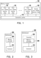
- FIG. 1 is a schematic circuit block diagram of a memory module according to an embodiment of the disclosure.
- FIG. 2 is a schematic circuit block diagram of a motherboard according to an embodiment of the disclosure.
- FIG. 3 is a schematic circuit block diagram of a motherboard according to another embodiment of the disclosure.
- FIG. 4 is a schematic circuit block diagram of a motherboard and a memory module according to an embodiment of the disclosure.
- FIG. 5 is a schematic circuit block diagram of a memory controller according to an embodiment of the disclosure.
- FIG. 6 is a schematic circuit block diagram of a memory controller and a plurality of memory modules according to an embodiment of the disclosure.
- FIG. 7 is a schematic circuit block diagram of a memory controller and a memory module according to an embodiment of the disclosure.
- Coupled may refer to any direct or indirect connection means.
- first device may be directly connected to the second device, or the first device may be indirectly connected through other devices or certain connection means to be connected to the second device.
- first”, second, and similar terms mentioned throughout the whole specification of the present application are merely used to name discrete elements or to differentiate among different embodiments or ranges. Therefore, the terms should not be regarded as limiting an upper limit or a lower limit of the quantity of the elements and should not be used to limit the arrangement sequence of elements.
- a rewritable non-volatile memory module includes a controller, a plurality of non-volatile memory chips (e.g., flash memory), a plurality of volatile memory chips (e.g., dynamic random access memory), and a built-in power supply.
- a host writes data to the memory module or reads data from the memory module. Specifically, the host accesses the memory chip through the controller of the memory module. Since the volatile memory chip requires a power supply for data to be stored, the memory module requires to be provided with a built-in power supply, so that in the event of a sudden power failure, the volatile memory chip stores data thereof in the non-volatile memory chip using the built-in power supply.
- the controller is provided on the motherboard, so one same one controller manages a plurality of memory modules at the same time, which solves the problem of heat dissipation.
- the memory modules in the following embodiments may not include a volatile memory chip, so the built-in power supply may be omitted.
- the interface between the memory module and the motherboard adopts the native interface of the non-volatile memory chip, so the memory module does not require to convert the native interface into a DDR interface. That is to say, for the memory module in the following embodiments may not be provided with the controller, the volatile memory chip, and the active power supply to save space. The space thus saved may accommodate more non-volatile memory chips, increasing the capacity of the memory module.
- FIG. 1 is a schematic circuit block diagram of a memory module according to an embodiment of the disclosure.
- a memory module 100 without a controller and without a built-in power supply includes at least one first non-volatile memory chip 101 , one second non-volatile memory chip 102 , and a connection portion 110 .
- the first non-volatile memory chip 101 and the second non-volatile memory chip 102 are respectively coupled to the connection portion 110 .
- the second non-volatile memory chip 102 may be configured to store at least one pointer of a meta data related to the first non-volatile memory chip 101 .
- the meta data may include at least one of address mapping information, bad block information, timing information, and namespace information of the first non-volatile memory chip, but the disclosure is not limited thereto.
- a memory type of the second non-volatile memory chip 102 may be different from a memory type of the first non-volatile memory chip 101 .
- the first non-volatile memory chip 101 may be a NAND flash memory chip or other flash memory
- the second non-volatile memory chip 102 may be an electrically-erasable programmable read-only memory (EEPROM) or other rewritable memory.
- the second non-volatile memory chip 102 may be coupled to the motherboard via the connection portion 110 adopting an inter-integrated circuit (I 2 C) interface or any other data transmission interface.
- I 2 C inter-integrated circuit
- the type of the first non-volatile memory chip 101 and the type of the second non-volatile memory chip 102 in this embodiment are not limited thereto.
- FIG. 2 is a schematic circuit block diagram of a motherboard 200 according to an embodiment of the disclosure
- FIG. 3 is a schematic circuit block diagram of the motherboard 200 according to another embodiment of the disclosure.
- the motherboard 200 includes a memory controller 300 and a connector 210 , and the memory controller 300 is coupled to the connector 210 .
- the connector 210 may be coupled to the connection portion 110 of the memory module 100 shown in FIG. 1 .
- the connector 210 may include a dual in-line memory module (DIMM) slot or any other type of connector, and the connection portion 110 may include a set of gold fingers or any other type of electrical connection mechanism.
- DIMM dual in-line memory module
- the memory controller 300 is provided being directly embedded on the motherboard 200 .
- the memory controller 300 may be provided on the converter 220 , and the converter 220 may be provided on the motherboard 200 .
- the converter 220 may include a peripheral component interconnect express (PCI-E) riser card, but this embodiment is not limited thereto. That is to say, the memory controller 300 may be provided on the motherboard 200 in the form of a PCI-E card.
- PCI-E peripheral component interconnect express
- the connection portion 110 of the memory module 100 is coupled to the connector 210 of the motherboard 200 .
- the memory controller 300 of the motherboard 200 accesses the first non-volatile memory chip 101 by a native interface of the first non-volatile memory chip 101 through the connector 210 .
- the native interface may include an open NAND flash interface (ONFI) or a TOGGLE interface.
- the memory controller 300 of the motherboard 200 may also access the pointer stored in the second non-volatile memory chip 102 of the memory module 100 through the connector 210 .
- the memory module 100 described in this embodiment is not provided with a memory controller and a built-in power supply circuit. Therefore, the memory module 100 provides additional space to accommodate more memory chips, thereby increasing the memory capacity of the memory module 100 and solving the problem of heat dissipation.
- FIG. 4 is a schematic circuit block diagram of the motherboard 200 and the memory module 100 according to an embodiment of the disclosure.
- the motherboard 200 has a central processing unit (CPU) 230 , a memory controller 300 , and four connectors 210 .
- the number of the connectors 210 is not limited thereto.
- the four connectors 210 are adapted to be respectively coupled to respective connection portions 110 of four memory modules 100 .
- the four memory modules 100 shown in FIG. 4 may be different memory modules 100 , such as memory modules 100 with different capacities, different operating frequencies, or different models. Since for the motherboard 200 , the memory controller 300 , and the connector 210 shown in FIG. 4 , reference may be made to the related description of FIG. 2 or FIG. 3 , and for the memory module 100 and the connection portion 110 shown in FIG. 4 reference may be made to the related description of FIG. 1 , the same will not be repeatedly described.
- the central processing unit 230 of the motherboard 200 may transmit a command to the memory controller 300 for accessing the four memory modules 100 .
- the conventional central processing unit requires to access each memory module via the respective controller of the memory module.
- the central processing unit 230 accesses the memory modules 100 via one single memory controller 300 , which reduces the workload of the central processing unit 230 . Therefore, the central processing unit 230 in general operates at a lower frequency, thereby reducing power consumption and reducing heat generated due to high-frequency operation.
- the memory controller 300 accesses the first non-volatile memory chip 101 on the memory module 100 (referring to the related description of FIG. 1 for details) via the native interface of the first non-volatile memory chip 101 . Therefore, the memory module 100 does not require to convert the native interface into the DDR interface.
- FIG. 5 is a schematic circuit block diagram of the memory controller 300 according to an embodiment of the disclosure. Depending on design requirements, in some embodiments, reference may be made to the related description of FIG. 5 for the memory controller 300 shown in FIG. 2 , FIG. 3 , or FIG. 4 .
- the memory controller 300 includes a finite state machine circuit 320 , a routing circuit 330 , a plurality of non-volatile memory controllers 310 , and one pointer load/store module 340 .
- One end of the routing circuit 330 is coupled to the finite state machine circuit 320
- the other end of the routing circuit 330 is coupled to the plurality of non-volatile memory controllers 310 .
- Each of the connectors 210 shown in FIG. 5 includes a plurality of data channels CHd and one meta channel CHm.
- Each of the non-volatile memory controllers 310 is adapted to be coupled to the corresponding channel (the data channel CHd or the meta channel CHm) of each of the plurality of connectors 210 of the motherboard 200 , to access the first non-volatile memory chip 101 of the memory module 100 through one of the connectors 210 .
- each of the non-volatile memory controllers 310 may manage the first non-volatile memory chip 101 of the memory module 100 coupled to any one of the connectors 210 through one corresponding data channel among the plurality of data channels CHd.
- FIG. 7 will provide a more detailed description.
- the non-volatile memory controller 310 may be a NAND flash controller (NFC) or any other controller.
- the NAND flash controller may be a conventional flash controller, and therefore will not be repeatedly described herein.
- the pointer load/store module 340 may access the second non-volatile memory chip 102 of the memory module 100 coupled to any one of the connectors 210 through a pointer channel CHp.
- the pointer load/store module 340 is coupled to the finite state machine circuit 320 to provide the pointer to a finite state machine set 321 of the finite state machine circuit 320 .
- the finite state machine circuit 320 includes a plurality of finite state machine sets 321 .
- the finite state machines 321 may implement a flash translation layer (FTL) function via hardware.
- the flash translation layer function includes operation such as address mapping, bad block management, garbage collection, wear leveling, and the like.
- a finite state machine set may include a plurality of finite state machines. Each finite state machine is in charge of a different function.
- the address of the data related to FTL may exist in form of pointers. That is, these pointers may be transmitted to NAND flash controller 310 through finite state machine set 321 to implement the FTL function.
- Each of the finite state machine sets 321 corresponds to one of the connectors 210 .
- a first finite state machine sets 321 may perform flash translation layer operation on the memory module 100 inserted in the first connector 210 .
- a fourth finite state machine sets 321 may perform flash translation layer operation on the memory module 100 inserted in a fourth connector 210 .
- the number of the finite state machine sets 321 is not limited thereto.
- the FTL function may be implemented by the finite state machine sets 321 , the workload of the central processing unit 230 is reduced. Therefore, the central processing unit 230 in general operates at a lower frequency, thereby reducing power consumption and reducing heat generated due to high-frequency operation.
- FIG. 6 is a schematic circuit block diagram of the memory controller 300 and a plurality of memory modules 100 according to an embodiment of the disclosure.
- the motherboard 200 includes four connectors 210 , four finite state machine sets 321 , and n+1 number of non-volatile memory controllers 310 .
- the finite state machine sets 321 , the routing circuit 330 , the non-volatile memory controllers 310 , the pointer load/store module 340 , and the connectors 210 shown in FIG. 6 reference may be made to the related description of FIG. 5 .
- the memory module 100 and the connection portion 110 shown in FIG. 6 reference may be made to the related description of FIG. 1 .
- the connector 210 (the memory module 100 ) have n+1 number of channels (referring to the related description of the data channel CHd and the meta channel CHm shown in FIG. 5 for details), and the memory controller 300 is thus provided with n+1 number of non-volatile memory controllers 310 .
- the n+1 number of channels include n number of data channels CHd and one meta channel CHm, where n is an integer determined depending on design requirements.
- the memory controller 300 accesses the first non-volatile memory chip 101 of the memory module 100 (referring to the related description of FIG. 1 for details) through the n+1 number of channels and the four connectors 210 .
- the pointer load/store module 340 is coupled to the finite state machine set 321 of the finite state machine circuit 320 .
- the pointer load/store module 340 is adapted to be coupled to the pointer channel CHp of each of the connectors 210 of the motherboard 200 .
- the pointer load/store module 340 in the memory controller 300 accesses the pointer stored in the second non-volatile memory chip 102 of the memory module 100 (refer to the related description of FIG. 1 for details) through the connector 210 and the pointer channel CHp.
- the pointer load/store module 340 may provide the pointer to the finite state machine set 321 of the finite state machine circuit 320 .
- the pointer load/store module 340 may store flash translation layer information of the four finite state machine set 321 (e.g., the address mapping information, the bad block management information, garbage collection information, wear leveling information, etc.) in the second non-volatile memory chip 102 of the memory module 100 (referring to the related description of FIG. 1 for details) through the pointer channel CHp and the connector 210 .
- the second non-volatile memory chip 102 may also store the namespace information and ONFI information of the memory module 100 to which it belongs.
- the namespace information includes partition information of the memory module 100 .
- the ONFI information includes information such as the capacity, the operating frequency, and the model of the memory module 100 .
- the flash translation layer information of the convention memory is stored in the block 0 of the flash memory chip.
- the block 0 is damaged, data in the entire flash memory chip cannot be read.
- the memory module 100 can still be read normally even if the block 0 of a certain first non-volatile memory chip 101 is damaged.
- the memory controller 300 may operate the four memory modules 100 with different capacities, different operating frequencies, or different models at the same time via the ONFI information.
- FIG. 7 is a schematic circuit block diagram of the memory controller 300 and the memory module 100 according to an embodiment of the disclosure.
- the memory controller 300 includes a finite state machine set 321 , nine non-volatile memory controllers, and one pointer load/store module 340 .
- the connector 210 includes nine corresponding general channels (eight data channels 251 to 258 and one meta channel 259 ) and one pointer channel 260 .
- the nine non-volatile memory controllers are respectively 1 st to 9 th non-volatile memory controller 351 to 359 .
- the 1 st to 8 th non-volatile memory controllers 351 to 358 correspond to the data channels 251 to 258
- the 9 th non-volatile memory controller 359 corresponds to the meta channel 259 .
- the memory module 100 includes nine memory chips.
- the nine memory chips are respectively 1 st to 9 th memory chips 151 - 159 .
- the 1 st to 9 th non-volatile memory controllers 351 to 359 respectively correspond to the 1 st to 9 th memory chips 151 to 159 .
- one end of the 1 st to 9 th non-volatile memory controllers 351 to 359 is coupled to the finite state machine set 321 through the routing circuit 330 , and the other end of the 1 st to 9 th non-volatile memory controllers 351 to 359 is respectively coupled to the 1 st to 9 th memory chips 151 to 159 of the memory module 100 through the general channels 251 to 259 .
- One end of the non-volatile memory controllers 351 - 359 is coupled to the 1 st to 9 th memory chips 151 - 159 through the connection portion 110 and the connector 210 .
- the finite state machine set 321 may issue a command (e.g., an access command, a management command, or any other command) to the 1 st to 9 th non-volatile memory controllers 351 to 359 through the routing circuit 330 .
- a command e.g., an access command, a management command, or any other command
- the non-volatile memory controllers 351 - 359 may perform corresponding operation on the memory chips 151 - 159 (e.g., access operation, management operation, or any other operation).
- the finite state machine set 321 is coupled to the connection portion 110 of the memory module 100 through the pointer load/store module 340 and then through the pointer channel 260 to access the second non-volatile memory chip 102 of the memory module 100 .
- the second non-volatile memory chip 102 may store at least one pointer of a meta data related to the first non-volatile memory chip 101 .
- the second non-volatile memory chip 102 may be EEPROM comprising an I 2 C interface, but the disclosure is not limited thereto.
- controllers of the plurality of memory modules are integrated into one controller on the motherboard, and an active power supply is not included.
- the memory module adopts the native interface of the memory chip as the pin, which does not require to be further converted into the DDR interface.
- the memory controller uses the state machine to implement the FTL function through hardware, and then stores the FTL information in the I 2 C EEPROM of the memory module. Therefore, the memory module provides additional space to accommodate more memory chips, which increases the capacity of the memory module, reduces the burden on the CPU, and solves the problem of heat dissipation.
- the host may operate different memory modules at the same time, and even if the block 0 of the memory chip in the memory module is damaged, the memory module can still be accessed normally.
Landscapes
- Engineering & Computer Science (AREA)
- Theoretical Computer Science (AREA)
- General Engineering & Computer Science (AREA)
- Physics & Mathematics (AREA)
- General Physics & Mathematics (AREA)
- Software Systems (AREA)
- Computer Hardware Design (AREA)
- Microelectronics & Electronic Packaging (AREA)
- Techniques For Improving Reliability Of Storages (AREA)
- Debugging And Monitoring (AREA)
Abstract
Description
Claims (20)
Priority Applications (3)
| Application Number | Priority Date | Filing Date | Title |
|---|---|---|---|
| US17/087,638 US11749335B2 (en) | 2020-11-03 | 2020-11-03 | Host and its memory module and memory controller |
| TW109140102A TWI781477B (en) | 2020-11-03 | 2020-11-17 | Host and its memory module and memory controller |
| CN202011396081.3A CN114443519B (en) | 2020-11-03 | 2020-12-03 | Host and its memory modules and memory controller |
Applications Claiming Priority (1)
| Application Number | Priority Date | Filing Date | Title |
|---|---|---|---|
| US17/087,638 US11749335B2 (en) | 2020-11-03 | 2020-11-03 | Host and its memory module and memory controller |
Publications (2)
| Publication Number | Publication Date |
|---|---|
| US20220139438A1 US20220139438A1 (en) | 2022-05-05 |
| US11749335B2 true US11749335B2 (en) | 2023-09-05 |
Family
ID=81361390
Family Applications (1)
| Application Number | Title | Priority Date | Filing Date |
|---|---|---|---|
| US17/087,638 Active 2041-07-17 US11749335B2 (en) | 2020-11-03 | 2020-11-03 | Host and its memory module and memory controller |
Country Status (3)
| Country | Link |
|---|---|
| US (1) | US11749335B2 (en) |
| CN (1) | CN114443519B (en) |
| TW (1) | TWI781477B (en) |
Families Citing this family (3)
| Publication number | Priority date | Publication date | Assignee | Title |
|---|---|---|---|---|
| US11749335B2 (en) * | 2020-11-03 | 2023-09-05 | Jianzhong Bi | Host and its memory module and memory controller |
| WO2024191737A1 (en) * | 2023-03-16 | 2024-09-19 | Micron Technology, Inc. | Configuring erase blocks coupled to a same string as zones |
| US20250355827A1 (en) * | 2024-05-20 | 2025-11-20 | Mellanox Technologies, Ltd. | Smart Serial Bus Interface Circuit |
Citations (23)
| Publication number | Priority date | Publication date | Assignee | Title |
|---|---|---|---|---|
| US5590340A (en) * | 1991-06-10 | 1996-12-31 | Matsushita Electric Industrial Co., Ltd. | Apparatus and method for suspending and resuming software application on a computer |
| US20020062429A1 (en) * | 2000-11-17 | 2002-05-23 | Masanao Tsuboki | Storage system and method for data transfer between storage systems |
| US20070028282A1 (en) * | 2003-09-12 | 2007-02-01 | Koninklijke Philips Electronics N.V. | Start up method for a television apparatus |
| US20070128899A1 (en) * | 2003-01-12 | 2007-06-07 | Yaron Mayer | System and method for improving the efficiency, comfort, and/or reliability in Operating Systems, such as for example Windows |
| US20070216688A1 (en) * | 2006-03-16 | 2007-09-20 | Seiko Epson Corporation | Display program, data structure and display device |
| TW200834585A (en) | 2006-09-28 | 2008-08-16 | Virident Systems Inc | Systems, methods, and apparatus for main memory with non-volatile type memory modules, and related technologies |
| US20090077284A1 (en) * | 2006-06-30 | 2009-03-19 | Mcm Portfolio Llc | System and Method for Enhancing External Storage |
| US20090150605A1 (en) * | 2007-12-06 | 2009-06-11 | David Flynn | Apparatus, system, and method for converting a storage request into an append data storage command |
| US20110010514A1 (en) * | 2009-07-07 | 2011-01-13 | International Business Machines Corporation | Adjusting Location of Tiered Storage Residence Based on Usage Patterns |
| TW201142605A (en) | 2009-11-25 | 2011-12-01 | Samsung Electronics Co Ltd | Multi-chip memory system and related data transfer method |
| CN102736861A (en) | 2011-04-08 | 2012-10-17 | 群联电子股份有限公司 | Memory configuration method, memory controller and memory storage device |
| TW201407468A (en) | 2012-04-20 | 2014-02-16 | 記憶體科技公司 | Manage operational status data in memory modules |
| US20150301754A1 (en) * | 2014-04-16 | 2015-10-22 | Sandisk Technologies Inc. | Storage Module and Method for Configuring the Storage Module with Memory Operation Parameters |
| US20180181510A1 (en) * | 2016-12-22 | 2018-06-28 | Integrated Device Technology, Inc. | Memory channel selection control |
| TWI674502B (en) | 2017-10-27 | 2019-10-11 | 日商東芝記憶體股份有限公司 | Memory system and control method |
| US20200169383A1 (en) * | 2019-06-29 | 2020-05-28 | Intel Corporation | Cryptographic computing engine for memory load and store units of a microarchitecture pipeline |
| US20200356396A1 (en) * | 2019-05-06 | 2020-11-12 | Micron Technology, Inc. | Class of service for multi-function devices |
| US20200401404A1 (en) * | 2019-06-18 | 2020-12-24 | EMC IP Holding Company LLC | Host processor configured with instruction set comprising resilient data move instructions |
| US10901886B2 (en) * | 2017-09-19 | 2021-01-26 | Shandong Storage Wings Electronics Technology Co., Ltd. | Hardware-based flash FTL function realization method and data storage device thereof |
| US11003527B2 (en) * | 2017-09-22 | 2021-05-11 | Shandong Storage Wings Electronics Technology Co., Ltd | Decoding method and device utilizing flash channel characteristic and data storage system |
| US20220139438A1 (en) * | 2020-11-03 | 2022-05-05 | Jianzhong Bi | Host and its memory module and memory controller |
| US20220284942A1 (en) * | 2021-03-05 | 2022-09-08 | Arm Limited | Memory Architecture with Pulsed-Bias Power |
| US20230075329A1 (en) * | 2021-08-25 | 2023-03-09 | Western Digital Technologies, Inc. | Super Block Allocation Across Super Device In ZNS SSD |
Family Cites Families (7)
| Publication number | Priority date | Publication date | Assignee | Title |
|---|---|---|---|---|
| US5432922A (en) * | 1993-08-23 | 1995-07-11 | International Business Machines Corporation | Digital storage system and method having alternating deferred updating of mirrored storage disks |
| US5983009A (en) * | 1996-10-03 | 1999-11-09 | Credence Systems Corporation | Automatic generation of user definable memory BIST circuitry |
| JP2005020349A (en) * | 2003-06-26 | 2005-01-20 | Renesas Technology Corp | Semiconductor integrated circuit and electronic system |
| TWI373773B (en) * | 2008-05-27 | 2012-10-01 | Phison Electronics Corp | Storage sysetm having multiple non-volatile memory, and controller and access method thereof |
| CN101609712B (en) * | 2008-06-18 | 2012-01-11 | 群联电子股份有限公司 | Storage system with multiple non-volatile memories, controller and access method thereof |
| US9753649B2 (en) * | 2014-10-27 | 2017-09-05 | Sandisk Technologies Llc | Tracking intermix of writes and un-map commands across power cycles |
| US11361215B2 (en) * | 2017-11-29 | 2022-06-14 | Anaflash Inc. | Neural network circuits having non-volatile synapse arrays |
-
2020
- 2020-11-03 US US17/087,638 patent/US11749335B2/en active Active
- 2020-11-17 TW TW109140102A patent/TWI781477B/en active
- 2020-12-03 CN CN202011396081.3A patent/CN114443519B/en active Active
Patent Citations (23)
| Publication number | Priority date | Publication date | Assignee | Title |
|---|---|---|---|---|
| US5590340A (en) * | 1991-06-10 | 1996-12-31 | Matsushita Electric Industrial Co., Ltd. | Apparatus and method for suspending and resuming software application on a computer |
| US20020062429A1 (en) * | 2000-11-17 | 2002-05-23 | Masanao Tsuboki | Storage system and method for data transfer between storage systems |
| US20070128899A1 (en) * | 2003-01-12 | 2007-06-07 | Yaron Mayer | System and method for improving the efficiency, comfort, and/or reliability in Operating Systems, such as for example Windows |
| US20070028282A1 (en) * | 2003-09-12 | 2007-02-01 | Koninklijke Philips Electronics N.V. | Start up method for a television apparatus |
| US20070216688A1 (en) * | 2006-03-16 | 2007-09-20 | Seiko Epson Corporation | Display program, data structure and display device |
| US20090077284A1 (en) * | 2006-06-30 | 2009-03-19 | Mcm Portfolio Llc | System and Method for Enhancing External Storage |
| TW200834585A (en) | 2006-09-28 | 2008-08-16 | Virident Systems Inc | Systems, methods, and apparatus for main memory with non-volatile type memory modules, and related technologies |
| US20090150605A1 (en) * | 2007-12-06 | 2009-06-11 | David Flynn | Apparatus, system, and method for converting a storage request into an append data storage command |
| US20110010514A1 (en) * | 2009-07-07 | 2011-01-13 | International Business Machines Corporation | Adjusting Location of Tiered Storage Residence Based on Usage Patterns |
| TW201142605A (en) | 2009-11-25 | 2011-12-01 | Samsung Electronics Co Ltd | Multi-chip memory system and related data transfer method |
| CN102736861A (en) | 2011-04-08 | 2012-10-17 | 群联电子股份有限公司 | Memory configuration method, memory controller and memory storage device |
| TW201407468A (en) | 2012-04-20 | 2014-02-16 | 記憶體科技公司 | Manage operational status data in memory modules |
| US20150301754A1 (en) * | 2014-04-16 | 2015-10-22 | Sandisk Technologies Inc. | Storage Module and Method for Configuring the Storage Module with Memory Operation Parameters |
| US20180181510A1 (en) * | 2016-12-22 | 2018-06-28 | Integrated Device Technology, Inc. | Memory channel selection control |
| US10901886B2 (en) * | 2017-09-19 | 2021-01-26 | Shandong Storage Wings Electronics Technology Co., Ltd. | Hardware-based flash FTL function realization method and data storage device thereof |
| US11003527B2 (en) * | 2017-09-22 | 2021-05-11 | Shandong Storage Wings Electronics Technology Co., Ltd | Decoding method and device utilizing flash channel characteristic and data storage system |
| TWI674502B (en) | 2017-10-27 | 2019-10-11 | 日商東芝記憶體股份有限公司 | Memory system and control method |
| US20200356396A1 (en) * | 2019-05-06 | 2020-11-12 | Micron Technology, Inc. | Class of service for multi-function devices |
| US20200401404A1 (en) * | 2019-06-18 | 2020-12-24 | EMC IP Holding Company LLC | Host processor configured with instruction set comprising resilient data move instructions |
| US20200169383A1 (en) * | 2019-06-29 | 2020-05-28 | Intel Corporation | Cryptographic computing engine for memory load and store units of a microarchitecture pipeline |
| US20220139438A1 (en) * | 2020-11-03 | 2022-05-05 | Jianzhong Bi | Host and its memory module and memory controller |
| US20220284942A1 (en) * | 2021-03-05 | 2022-09-08 | Arm Limited | Memory Architecture with Pulsed-Bias Power |
| US20230075329A1 (en) * | 2021-08-25 | 2023-03-09 | Western Digital Technologies, Inc. | Super Block Allocation Across Super Device In ZNS SSD |
Non-Patent Citations (1)
| Title |
|---|
| "Office Action of Taiwan Counterpart Application", dated Mar. 8, 2022, p. 1-p. 3. |
Also Published As
| Publication number | Publication date |
|---|---|
| TW202219776A (en) | 2022-05-16 |
| US20220139438A1 (en) | 2022-05-05 |
| CN114443519B (en) | 2024-09-03 |
| CN114443519A (en) | 2022-05-06 |
| TWI781477B (en) | 2022-10-21 |
Similar Documents
| Publication | Publication Date | Title |
|---|---|---|
| US9158716B2 (en) | Memory controller supporting concurrent volatile and nonvolatile memory modules in a memory bus architecture | |
| US11749335B2 (en) | Host and its memory module and memory controller | |
| US8402208B2 (en) | Configurable memory controller/memory module communication system | |
| US8832404B2 (en) | Memory hub with integrated non-volatile memory | |
| US7983051B2 (en) | DRAM module with solid state disk | |
| US8694721B2 (en) | Memory buffer with one or more auxiliary interfaces | |
| US9058257B2 (en) | Persistent block storage attached to memory bus | |
| US20080229049A1 (en) | Processor card for blade server and process. | |
| US20110235260A1 (en) | Dram module with solid state disk | |
| US9910612B2 (en) | Memory buffer with one or more auxiliary interfaces | |
| CN112631954B (en) | Expandable Dual In-line Memory Module | |
| KR20150007208A (en) | Ina cabled memory appliance | |
| CN112513824B (en) | Memory interleaving method and device | |
| US10831963B1 (en) | Apparatus and method of parallel architecture for NVDIMM | |
| US7752429B2 (en) | Computer system and boot code accessing method thereof | |
| US11693814B2 (en) | Systems and methods for expanding memory access | |
| US9792207B2 (en) | Data storage in a mobile device with embedded mass storage device | |
| US11221931B2 (en) | Memory system and data processing system | |
| CN101582037A (en) | Method for sharing basic input and output system, blade server and computer thereof | |
| KR20160004728A (en) | Memory system and data storage device | |
| CN201072552Y (en) | memory control system |
Legal Events
| Date | Code | Title | Description |
|---|---|---|---|
| FEPP | Fee payment procedure |
Free format text: ENTITY STATUS SET TO UNDISCOUNTED (ORIGINAL EVENT CODE: BIG.); ENTITY STATUS OF PATENT OWNER: SMALL ENTITY |
|
| FEPP | Fee payment procedure |
Free format text: ENTITY STATUS SET TO SMALL (ORIGINAL EVENT CODE: SMAL); ENTITY STATUS OF PATENT OWNER: SMALL ENTITY |
|
| AS | Assignment |
Owner name: SHANDONG STORAGE WINGS ELECTRONICS TECHNOLOGY CO., LTD, CHINA Free format text: ASSIGNMENT OF ASSIGNORS INTEREST;ASSIGNOR:BI, JIANZHONG;REEL/FRAME:054319/0092 Effective date: 20201008 Owner name: BI, JIANZHONG, CHINA Free format text: ASSIGNMENT OF ASSIGNORS INTEREST;ASSIGNOR:BI, JIANZHONG;REEL/FRAME:054319/0092 Effective date: 20201008 |
|
| STPP | Information on status: patent application and granting procedure in general |
Free format text: DOCKETED NEW CASE - READY FOR EXAMINATION |
|
| STPP | Information on status: patent application and granting procedure in general |
Free format text: NON FINAL ACTION MAILED |
|
| STPP | Information on status: patent application and granting procedure in general |
Free format text: RESPONSE TO NON-FINAL OFFICE ACTION ENTERED AND FORWARDED TO EXAMINER |
|
| STPP | Information on status: patent application and granting procedure in general |
Free format text: NOTICE OF ALLOWANCE MAILED -- APPLICATION RECEIVED IN OFFICE OF PUBLICATIONS |
|
| STCF | Information on status: patent grant |
Free format text: PATENTED CASE |
|
| AS | Assignment |
Owner name: JIANZHONG BI, CHINA Free format text: ASSIGNMENT OF ASSIGNORS INTEREST;ASSIGNORS:JIANZHONG BI;SHANDONG STORAGE WINGS ELECTRONICS TECHNOLOGY CO., LTD;REEL/FRAME:066355/0857 Effective date: 20240119 Owner name: ADVANCED STORAGE TECHNOLOGY CO., LTD, TAIWAN Free format text: ASSIGNMENT OF ASSIGNORS INTEREST;ASSIGNORS:JIANZHONG BI;SHANDONG STORAGE WINGS ELECTRONICS TECHNOLOGY CO., LTD;REEL/FRAME:066355/0857 Effective date: 20240119 |