US11716150B2 - Field reconstruction for an optical receiver - Google Patents
Field reconstruction for an optical receiver Download PDFInfo
- Publication number
- US11716150B2 US11716150B2 US16/811,194 US202016811194A US11716150B2 US 11716150 B2 US11716150 B2 US 11716150B2 US 202016811194 A US202016811194 A US 202016811194A US 11716150 B2 US11716150 B2 US 11716150B2
- Authority
- US
- United States
- Prior art keywords
- optical
- signal
- digital
- data
- frequency
- Prior art date
- Legal status (The legal status is an assumption and is not a legal conclusion. Google has not performed a legal analysis and makes no representation as to the accuracy of the status listed.)
- Active
Links
Images


Classifications
-
- H—ELECTRICITY
- H04—ELECTRIC COMMUNICATION TECHNIQUE
- H04B—TRANSMISSION
- H04B10/00—Transmission systems employing electromagnetic waves other than radio-waves, e.g. infrared, visible or ultraviolet light, or employing corpuscular radiation, e.g. quantum communication
- H04B10/60—Receivers
- H04B10/66—Non-coherent receivers, e.g. using direct detection
- H04B10/69—Electrical arrangements in the receiver
- H04B10/691—Arrangements for optimizing the photodetector in the receiver
- H04B10/6911—Photodiode bias control, e.g. for compensating temperature variations
-
- H—ELECTRICITY
- H04—ELECTRIC COMMUNICATION TECHNIQUE
- H04B—TRANSMISSION
- H04B10/00—Transmission systems employing electromagnetic waves other than radio-waves, e.g. infrared, visible or ultraviolet light, or employing corpuscular radiation, e.g. quantum communication
- H04B10/60—Receivers
- H04B10/66—Non-coherent receivers, e.g. using direct detection
- H04B10/69—Electrical arrangements in the receiver
- H04B10/693—Arrangements for optimizing the preamplifier in the receiver
- H04B10/6932—Bandwidth control of bit rate adaptation
-
- H—ELECTRICITY
- H04—ELECTRIC COMMUNICATION TECHNIQUE
- H04B—TRANSMISSION
- H04B10/00—Transmission systems employing electromagnetic waves other than radio-waves, e.g. infrared, visible or ultraviolet light, or employing corpuscular radiation, e.g. quantum communication
- H04B10/60—Receivers
- H04B10/66—Non-coherent receivers, e.g. using direct detection
- H04B10/69—Electrical arrangements in the receiver
- H04B10/693—Arrangements for optimizing the preamplifier in the receiver
- H04B10/6933—Offset control of the differential preamplifier
-
- H—ELECTRICITY
- H04—ELECTRIC COMMUNICATION TECHNIQUE
- H04B—TRANSMISSION
- H04B10/00—Transmission systems employing electromagnetic waves other than radio-waves, e.g. infrared, visible or ultraviolet light, or employing corpuscular radiation, e.g. quantum communication
- H04B10/60—Receivers
- H04B10/66—Non-coherent receivers, e.g. using direct detection
- H04B10/69—Electrical arrangements in the receiver
- H04B10/697—Arrangements for reducing noise and distortion
Definitions
- Various example embodiments relate to optical communication equipment and, more specifically but not exclusively, to optical transmitters and receivers.
- Some optical receivers are capable of detecting not only the amplitude of an optical signal, but also the signal's phase. As a result, the optical field can substantially be reconstructed at the receiver and then be used for signal equalization, e.g., directed at reducing the adverse effects of some optical-link impairments, such as chromatic dispersion (CD), polarization-mode dispersion (PMD), etc.
- CD chromatic dispersion
- PMD polarization-mode dispersion
- a direct-detection optical receiver capable of substantially measuring the phase and amplitude of a received intensity- or amplitude-modulated optical signal by performing digital signal processing.
- a digital signal processor (DSP) of the receiver operates to reduce the detrimental effects of relative phase noise between the optical reference oscillator and optical carrier based on an optical pilot present in the received optical signal.
- the DSP may employ a sequence of digital filters configured to select a signal component that represents a non-vestigial modulation sideband and then perform signal equalization thereon.
- the signal equalization may include but is not limited to dispersion compensation.
- the optical receiver may be a square-law-detector-based optical receiver.
- the optical reference oscillator and optical carrier may be generated using two respective independently running lasers that may or may not be co-located.
- an apparatus comprising an optical data receiver that comprises: a photodiode detector; and a digital signal processor connected to receive digital measurements of light by the photodiode detector at a sequence of times, the digital signal processor being configured to recover a data stream of an optical input signal from the digital measurements, each of the measurements measuring one or more combinations of the optical input signal and an optical frequency reference at one of times, the optical input signal having a data component produced by data-modulating an optical carrier and a pilot peak produced by modulating the optical carrier with a pilot frequency tone; and wherein the digital signal processor is configured to adjust said digital measurements to compensate for a frequency offset of the optical carrier with respect to the optical frequency reference based on evaluations of a phase or frequency of the pilot peak.
- an apparatus comprising an optical data receiver that comprises: a front-end circuit; and a digital signal processor connected to receive, from the front-end circuit, digital measurements of one or more combinations of an optical input signal and an optical frequency reference at corresponding times, the optical input signal including a data band and a pilot peak produced by modulating an optical carrier with a data stream and a pilot frequency tone, respectively; wherein the front-end circuit has a narrower output bandwidth than a bandwidth of the one or more combinations of the optical input signal and the optical frequency reference; and wherein the digital signal processor is configured to determine the data stream modulated onto the optical carrier by adjusting the digital measurements to compensate for a frequency offset between the optical input signal and the optical frequency reference based on estimations from the digital measurements of a phase or frequency of the pilot peak of the optical input signal.
- an apparatus comprising an optical data receiver that comprises a front-end circuit connected to a signal processor, the front-end circuit including a photodetector configured to generate an electrical output signal in response to an optical input signal applied thereto; wherein the front-end circuit has a limited electrical bandwidth with respect to an optical bandwidth of the optical input signal, the optical bandwidth including an optical reference oscillator and modulation sidebands of an optical carrier; and wherein the signal processor is capable of digitally reconstructing an optical field of the optical input signal by processing a digital form of the electrical output signal using a signal component thereof corresponding to an optical pilot present in the optical input signal.
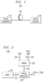
- FIG. 1 shows a block diagram of an example optical fiber communication system in which some embodiments may be practiced
- FIG. 2 shows a block diagram of an optical data transmitter that can be used in the optical fiber communication system of FIG. 1 according to an embodiment
- FIGS. 3 A- 3 B graphically illustrate example spectral characteristics of optical output signals that may be generated by some embodiments of the optical data transmitter shown in FIG. 2 ;
- FIG. 4 shows a block diagram of an optical data transmitter that can be used in the optical communication system of FIG. 1 according to another embodiment
- FIGS. 5 A- 5 C graphically illustrate example spectral characteristics of optical output signals that may be generated by some embodiments of the optical data transmitter shown in FIG. 4 ;
- FIG. 6 shows a block diagram of a direct-detection, optical data receiver that can be used in the optical fiber communication system of FIG. 1 according to an embodiment
- FIGS. 7 A- 7 B graphically illustrate example spectral characteristics of electrical signals that may be generated by some embodiments of the direct-detection, optical data receiver shown in FIG. 6 ;
- FIG. 8 shows a block diagram of an optical data receiver that can be used in the optical fiber communication system of FIG. 1 according to another embodiment
- FIG. 9 shows a block diagram of an optical data receiver that can be used in the optical fiber communication system of FIG. 1 according to yet another embodiment
- FIG. 10 shows a block diagram of a digital circuit that can be used in the optical data receiver of FIG. 9 according to an embodiment
- FIGS. 11 A- 11 F graphically illustrate example spectral characteristics of some digital electrical signals that may be generated in the digital circuit of FIG. 10 according to an embodiment
- FIG. 12 shows a block diagram of a digital circuit that can be used in the optical data receiver of FIG. 6 or FIG. 8 according to an embodiment
- FIG. 13 shows a flowchart of a signal-processing method that can be implemented in in the optical data receiver of FIG. 6 or FIG. 8 according to an embodiment
- FIG. 14 graphically illustrates examples of potential performance improvements according to an embodiment.
- the Kramers-Kronig (KK) algorithm is a conventional field-reconstruction algorithm that may be used in some direct-detection optical receivers.
- the KK algorithm is reviewed, e.g., in A. Mecozzi, et al., “Kramers-Kronig Coherent Receiver,” Optica 3 , pp. 1218-1227 (2016), which is incorporated herein by reference in its entirety.
- optical-field reconstruction means determination of amplitude and phase of an optical signal, e.g., average amplitudes and phases for individual signal slots. Such optical-field reconstruction may or may not involve determining the amplitude and phase of both polarization components of the optical signal.
- a direct-detection optical receiver may be configured to receive a data-carrying optical signal and an optical frequency-reference signal (e.g., an optical oscillator) together, e.g., from a remote optical transmitter, and to recover data from the data-carrying optical signal based on interference between the received data-carrying and frequency-reference signals in a light detector.
- the light detector is configured to measure only light intensities, e.g., the light detector may be a single photodiode.
- the optical frequency-reference signal typically has a much narrower bandwidth than the data-carrying optical signal.
- a direct-detection optical receiver does not employ an optical hybrid or an optical local oscillator to perform such data recovery and notably, does not use optical interference of said received optical signal with another light signal to determine the data carried by the data-carrying optical signal.
- FIG. 1 shows a block diagram of an example optical fiber communication system 100 in which some embodiments may be practiced.
- System 100 comprises an optical data transmitter 110 and an optical data receiver 130 optically connected via an optical fiber communication link 120 .
- link 120 comprises one or more spans of optical fiber or fiber-optic cable, e.g., one or more spans of standard single-mode optical fiber.
- link 120 may include one or more optional optical amplifiers (not explicitly shown in FIG. 1 ), each connected between two corresponding fiber spans.
- link 120 may include other optical elements, e.g., one or more optical filters, splitters, switches, etc.
- link 120 may be implemented using planar optical waveguides and/or free-space optical connections.
- the distance between optical data transmitter 110 and optical data receiver 130 is between 1 km and 100 km, e.g., including lengths that are short enough to avoid the use of in-line optical amplification, such as example lengths encountered in intra-datacenter optical communications.
- Example embodiments of optical data transmitter 110 are described in reference to FIGS. 2 - 5 .
- Example embodiments of optical data receiver 130 are described in reference to FIGS. 6 - 14 .
- FIG. 2 shows a block diagram of optical data transmitter 110 according to an embodiment. This particular embodiment of optical data transmitter 110 is labeled 110 a .
- Transmitter 110 a comprises a laser source 210 , an optical modulator 220 , and an electrical drive circuit 230 connected as indicated in FIG. 2 .
- laser source 210 generates an optical carrier 212 having a carrier frequency f c .
- Optical modulator 220 then operates to modulate optical carrier 212 in response to an electrical drive signal 228 .
- a resulting modulated optical signal 222 may then be applied to optical communication link 120 (also see FIG. 1 ).
- optical modulator 220 can be an optical intensity modulator, e.g., an electro-absorption modulator (EAM).
- EAM electro-absorption modulator
- an electrical pilot-tone signal 234 indicated in FIG. 2 by the dashed arrow is not present or not used, and drive circuit 230 is configured to generate electrical drive signal 228 , as known in the pertinent art, in response to an electrical data signal 232 .
- Electrical data signal 232 may be an amplitude-modulated electrical data signal.
- electrical data signal 232 can be a real-valued signal and/or can be represented by a sequence of real values. An example spectrum of the resulting modulated optical signal 222 a is described below in reference to FIG. 3 A .
- optical modulator 220 can be an optical amplitude modulator, such as a Mach-Zehnder modulator (MZM) or an IQ modulator configured for pulse-amplitude modulation (PAM).
- drive circuit 230 is configured to generate electrical drive signal 228 , as known in the pertinent art, in response to electrical data signal 232 and electrical pilot-tone signal 234 having a radio frequency f RF .
- An example spectrum of the resulting modulated optical signal 222 b is described below in reference to FIG. 3 B .
- electrical pilot-tone signal 234 may have predefined frequency and phase characteristics.
- electrical pilot-tone signal 234 may be a sinusoidal wave having a fixed (i.e., constant) frequency and amplitude.
- electrical pilot-tone signal 234 may be controllably slowly dithered.
- slowly means that the one or more frequencies, with which the frequency f RF and/or amplitude of the pilot tone are modulated (dithered), are much smaller than the time-averaged frequency ⁇ f RF >.
- the frequency f may be selected such that, in optical signal 222 b , an optical pilot corresponding to the electrical pilot-tone signal 234 is substantially out-of-band with respect to the data signal (also see FIG. 3 B ).
- the frequency f RF may be selected such that an optical pilot corresponding to the electrical pilot-tone signal 234 is in-band with respect to the data signal.
- Drive circuit 230 may include, inter alia, conventional electrical circuitry for properly combining electrical data signal 232 and electrical pilot-tone signal 234 .
- an analog signal combiner or a digital adder may be used for this purpose as known in the pertinent art.
- a resulting combined signal may be amplified and optionally dc-biased to generate electrical drive signal 228 .
- electrical signal 232 may be any real-valued time-dependent electrical waveform W(t), where t is time.
- the waveform W(t) may not necessarily have encoded therein a data stream for transmission over a sequence of discrete time slots. Rather, the waveform W(t) may represent some analog “message” or signal.
- optical signal 222 b is generated by concurrently using electrical data signal 232 and electrical pilot-tone signal 234 to generate the corresponding electrical drive signal 228 .
- modulated optical signal 222 b concurrently carries a data component (e.g., modulation sidebands S and S*) and at least one pilot peak (e.g., 312 2 ), e.g., as illustrated in FIG. 3 B .
- FIG. 3 A graphically illustrates example spectral characteristics of modulated optical signal 222 a according to an embodiment.
- optical signal 222 a is generated by intensity modulation of optical carrier 212 .
- the spectrum, S(f) of modulated optical signal 222 a comprises modulation sidebands S and S* that are Hermitian-symmetric with respect to the carrier frequency f c .
- the spectrum of modulated optical signal 222 a further comprises a residual optical carrier 302 .
- the intensity modulation in optical modulator 220 transfers some of the optical energy from the input optical carrier 212 into modulation sidebands S and S*, the input optical carrier is typically not fully depleted.
- the resulting attenuated optical carrier thus appears in the spectrum of modulated optical signal 222 a as residual optical carrier 302 .
- FIG. 3 B graphically illustrates example spectral characteristics of modulated optical signal 222 b according to an embodiment.
- modulated optical signal 222 b is generated by amplitude modulation of optical carrier 212 .
- the amplitude modulation used herein substantially fully depletes the input optical carrier 212 .
- a residual optical carrier similar to the residual optical carrier 302 ( FIG. 3 A ) is not present in the spectrum of modulated optical signal 222 b.
- the spectrum of modulated optical signal 222 b comprises Hermitian-symmetric modulation sidebands S and S.
- the spectrum of modulated optical signal 222 b further comprises optical pilots 312 1 and 312 2 generated in response to the electrical pilot-tone signal 234 .
- Optical pilot 312 1 has an optical frequency of (f c ⁇ f RF ).
- Optical pilot 312 2 has an optical frequency of (f c +f RF ).
- the frequency f RF is selected such that f RF >B/2, where B is the 3-dB bandwidth of the data-modulated signal (S*, S). This f RF -value selection results in little or no overlap between the optical pilots 312 1 and 312 2 and data-modulated signal (S*, S), e.g., as graphically indicated in FIG. 3 B .
- modulated optical signal 222 b has a data component (e.g., modulation sidebands S and S*) and at least one pilot peak (e.g., 312 2 ) formed by concurrently modulating the same optical carrier (e.g., 212 ) with a data stream (e.g., 232 ) and a pilot frequency tone (e.g., 234 ), respectively.
- a data component e.g., modulation sidebands S and S*
- at least one pilot peak e.g., 312 2
- a data stream e.g., 232
- a pilot frequency tone e.g., 234
- FIG. 4 shows a block diagram of optical data transmitter 110 according to an alternative embodiment.
- This particular embodiment of optical data transmitter 110 is labeled 110 b .
- Transmitter 110 b comprises optical data transmitter 110 a ( FIG. 2 ), a laser source 410 , and an optical combiner 420 connected as indicated in FIG. 4 .
- Laser source 410 is configured to generate an optical frequency-reference oscillator 412 having an optical frequency f ref .
- Optical combiner 420 operates to optically combine the modulated optical signal 222 a or 222 b generated (as described above) by transmitter 110 a and optical frequency-reference oscillator 412 .
- a resulting modulated optical signal 422 a or 422 b may then be applied to optical communication link 120 (also see FIG. 1 ).
- each of laser sources 210 and 410 may be a free-running laser.
- optical signals 212 and 412 may not be frequency-locked or phase-locked to one another.
- optical signals 212 and 412 may have relatively uncorrelated phase noise.
- optical pilots 312 1 and 312 2 FIGS. 3 B, 5 B ) have relatively correlated phase noise with optical carrier 212 by virtue of being produced by low-noise RF modulation thereof.
- FIG. 5 A graphically illustrates example spectral characteristics of modulated optical signal 422 a according to an embodiment.
- Modulated optical signal 422 a is generated in transmitter 110 b ( FIG. 4 ) by combining (i) modulated optical signal 222 a ( FIG. 3 A ) generated as described above by transmitter 110 a and (ii) optical frequency-reference oscillator 412 generated by laser source 410 .
- the optical frequency f ref is greater than the optical carrier frequency f c , i.e., f ref >f c .
- the optical frequency f ref can be smaller than the optical carrier frequency f c , i.e., f ref ⁇ f c .
- Modulated optical signal 422 a has an optical bandwidth B OS that is indicated in FIG. 5 A . Note that typically B OS >B. However, in some embodiments, optical frequency-reference oscillator 412 may be slightly in band.
- FIG. 5 B graphically illustrates example spectral characteristics of modulated optical signal 422 b according to an embodiment.
- Modulated optical signal 422 b is generated in transmitter 110 b ( FIG. 4 ) by combining (i) modulated optical signal 222 b ( FIG. 3 B ) generated as described above by transmitter 110 a and (ii) optical frequency-reference oscillator 412 generated by laser source 410 .
- the optical reference oscillator's frequency f ref is typically selected such that the frequency f RF is smaller than the absolute value of the difference between the optical frequencies f ref and f c , i.e.,
- Modulated optical signal 422 b has an optical bandwidth B OS that is indicated in FIG. 5 B .
- FIG. 5 C graphically illustrates an alternative embodiment, in which the optical reference oscillator's frequency f ref is selected such that the frequency f is greater than the absolute value of the difference between the optical frequencies f ref and f e , i.e.,
- FIG. 6 shows a block diagram of optical data receiver 130 according to an embodiment.
- This particular embodiment of optical data receiver 130 is labeled 130 a .
- Receiver 130 a comprises a photodetector 610 , an analog-to-digital converter (ADC) 620 , and a digital signal processor (DSP) 630 .
- ADC analog-to-digital converter
- DSP digital signal processor
- receiver 130 a is configured to receive modulated optical signal 422 a or 422 b (also see FIGS. 5 A- 5 B ).
- receiver 130 a can be paired up with transmitter 110 b ( FIG. 4 ).
- photodetector 610 may comprise a single photodiode (e.g., 602 ) and a transimpedance amplifier (TIA; e.g., 604 ) connected in a single-ended electrical configuration.
- the photodiode is connected to receive light of the modulated optical signal 422 a or 422 b through link 120 and apply the resulting electrical signal to the TIA.
- a corresponding amplified electrical signal 612 generated by the TIA is then converted into digital form by ADC 620 , and a resulting digital electrical signal 622 is applied to digital signal processor (DSP) 130 for processing and data recovery therein.
- DSP digital signal processor
- single-ended refers to an electrical configuration in which the photocurrent generated by a single photodiode is being sensed and/or measured by the corresponding electrical circuit (e.g., a TIA) connected to the photodiode.
- the single photodiode so connected has a single optical input, a single electrical output, and a p-n junction that converts light received at the optical input into electrical current at the electrical output.
- a single-ended electrical configuration should be contrasted with a balanced or differential electrical configuration in which the photocurrents generated by two serially connected photodiodes are driven through a common electrical terminal, and the combined photocurrent flowing through the common electrical terminal is sensed and/or measured by the corresponding electrical circuit connected thereto.
- a typical balanced photodetector has two optical inputs, one electrical output, and two nominally identical constituent photodiodes having separate and distinct p-n junctions. The electrical output is between the connected photodiodes.
- the quality of a balanced photodetector so constructed typically depends on the extent to which the two constituent photodiodes are matched to one another.
- the optoelectronic front end of receiver 130 may have a 3-dB bandwidth B Rx ), (e.g., see FIG. 7 A ) that is limited with respect to the bandwidth of modulated optical signal 422 a or 422 b .
- the optoelectronic front end of receiver 130 a ( FIG. 6 ) may include photodetector 610 and possibly some other associated circuitry, such as ADC 620 .
- the term “limited” means that the bandwidth B Rx is smaller than the optical bandwidth B OS .
- the bandwidth B Rx may approximately satisfy the following inequality:
- the bandwidth B Rx can be in the range between 55% and 90% of B OS .
- FIG. 7 A graphically illustrates example spectral characteristics of electrical signal 612 a generated in receiver 130 a ( FIG. 6 ) according to an embodiment. More specifically, photodetector 610 may generate electrical signal 612 a in response to modulated optical signal 422 a , said electrical signal being the down-converted beat frequency signal corresponding to the modulated optical signal at a non-zero intermediate frequency.
- the zero frequency in the spectrum of electrical signal 612 a corresponds to the optical frequency f ref (also see FIG. 5 A ).
- the spectrum of electrical signal 612 a comprises data bands 704 1 and 704 2 , narrow spectral bands (e.g., spectral lines) 706 1 and 706 2 , and an SSBI band 708 .
- SSBI stands for signal-to-signal beat interference.
- Data bands 704 1 and 704 2 are generated by photodetector 610 by down-converting and performing band-limiting filtering of the data-modulated optical signal (S*, S) (also see FIG. 5 A ).
- the down-conversion causes data bands 704 1 and 704 2 to be relatively symmetric with respect to the zero frequency.
- the band-limiting filtering is represented in FIG. 7 A by an effective transfer function 702 of the front end of receiver 130 a .
- the transfer function 702 has a 3-dB bandwidth of approximately 2B Rx , as indicated in FIG. 7 A (also see Eq. (1)).
- Narrow spectral bands 706 1 and 706 2 are generated by photodetector 610 by down-converting the residual optical carrier 302 .
- the down-conversion causes narrow spectral bands 706 1 and 706 2 to be symmetric with respect to the zero frequency.
- Data band 704 1 has two sub-bands, which are indicated by different hatching in FIG. 7 A .
- the first one of these two sub-bands is located to the left of (i.e., farther away from the zero frequency than) narrow spectral band 706 1
- the second one of these two sub-bands is located to the right of (i.e., closer to the zero frequency than) narrow spectral band 706 1 .
- the second sub-band corresponds to the optical modulation sideband S
- the first sub-band corresponds to the optical modulation sideband S* (also see FIG. 5 A ).
- the band-limiting filtering represented by the transfer function 702 causes the first sub-band to be spectrally narrower than the second sub-band.
- the first and second sub-bands may be referred to as the vestigial sub-band and non-vestigial sub-band, respectively.
- Data band 704 2 also has two sub-bands, which are indicated in FIG. 7 A by different hatching therein.
- a person of ordinary skill in the art will understand that the sub-bands of data band 704 2 are qualitatively similar to the above-described sub-bands of data bands 704 1 .
- SSBI band 708 is generated by photodetector 610 due to the presence of signal-to-signal beat products in the output thereof.
- the SSBI may be detrimental in that it can significantly reduce the effective signal-to-noise ratio (SNR).
- SNR signal-to-noise ratio
- the detrimental effects of SSBI can be substantially canceled in DSP 630 , e.g., as described below in reference to FIGS. 12 - 13 .
- FIG. 7 B graphically illustrates example spectral characteristics of electrical signal 612 b generated in receiver 130 a ( FIG. 6 ) according to an embodiment. More specifically, photodetector 610 may generate electrical signal 612 b in response to modulated optical signal 422 b , said electrical signal being the down-converted beat frequency signal corresponding to the modulated optical signal at a non-zero intermediate frequency.
- the zero frequency in the spectrum of electrical signal 612 b corresponds to the optical frequency f ref (also see FIG. 5 B ).
- the spectrum of electrical signal 612 b comprises data bands 704 1 and 704 2 and SSBI band 708 .
- narrow spectral bands 706 1 and 706 2 are not present therein.
- the spectrum of electrical signal 612 b has narrow spectral bands (e.g., spectral lines) 710 1 and 710 2 , both of which are generated by down-converting the optical pilot 312 2 (see FIG. 5 B ).
- the pilot peak 312 1 is filtered out due to being outside the bandwidth B R ), of the front end of receiver 130 a.
- FIG. 8 shows a block diagram of optical data receiver 130 according to another embodiment.
- This particular embodiment of optical data receiver 130 is labeled 130 b .
- receiver 130 b is configured to receive modulated optical signal 222 a or 222 b (also see FIGS. 3 A- 3 B ).
- transmitter 110 a FIG. 2 ).
- Receiver 130 b comprises receiver 130 a , laser source 410 , and optical combiner 420 connected as indicated in FIG. 8 .
- Example functions and characteristics of laser source 410 and optical combiner 420 have been described above in reference to FIG. 4 . Note however that, in the embodiment of FIG. 4 , laser source 410 and optical combiner 420 are located at the corresponding transmitter 110 . In contrast, in this embodiment, laser source 410 and optical combiner 420 are located at receiver 130 .
- the optical output signal 422 a or 422 b generated by optical combiner 420 in receiver 130 b is applied to the constituent receiver 130 a , which processes this signal as described above in reference to FIGS. 6 , 7 A , and 7 B.
- Example spectra of electrical signals 612 a and 612 b generated in receiver 130 b are shown in FIGS. 7 A and 7 B , respectively.
- FIG. 9 shows a block diagram of optical data receiver 130 according to yet another embodiment.
- This particular embodiment of optical data receiver 130 is labeled 130 c .
- receiver 130 c is configured to receive modulated optical signal 222 a or 222 b (also see FIGS. 3 A- 3 B ).
- transmitter 110 a FIG. 2 ).
- Receiver 130 c is a modification of receiver 130 b ( FIG. 8 ) obtained by making the following changes.
- Optical combiner 420 ( FIG. 8 ) is replaced by a 180-degree optical hybrid 920 .
- the single photodiode 602 of photodetector 610 is replaced by photodiodes 930 1 and 930 2 connected in a differential configuration, with the common electrical terminal being connected to a TIA 940 .
- TIA 940 may be of the same type as TIA 604 used in photodetector 610 .
- TIA 940 outputs an electrical signal 942 a when receiver 130 c receives modulated optical signal 222 a .
- electrical signal 942 a has a spectrum similar to that shown in FIG. 7 A , except that the SSBI band 708 may not be present therein.
- a well-balanced differential photodetector cancels the SSBI of the constituent individual photodiodes by subtracting the corresponding signal-to-signal beat products at the common terminal thereof.
- TIA 940 outputs an electrical signal 942 b when receiver 130 c receives modulated optical signal 222 b .
- electrical signal 942 b has a spectrum similar to that shown in FIG. 7 B , except that the SSBI band 708 may not be present therein for the above-explained reason.
- FIG. 10 shows a block diagram of a digital circuit 1000 that can be used in DSP 630 according to an embodiment.
- circuit 1000 is described in reference to its example use in receiver 130 c ( FIG. 9 ) and with continued reference to FIGS. 11 A- 11 F .
- circuit 1000 processes digital signal 622 to recover the corresponding electrical data signal 232 (also see FIG. 2 ).
- circuit 1000 comprises the following digital circuits connected as indicated in FIG. 10 : (i) Hilbert-transform (HT) circuits 1010 and 1050 ; (ii) a pilot-extraction circuit 1020 ; (iii) a phase-correction circuit 1030 ; (iv) a frequency down-converter 1040 ; (v) a dispersion compensator (CD ⁇ 1 ) 1060 ; (vi) an equalizer 1070 ; and (vii) a complex-to-real (C/R) signal converter 1080 .
- HT Hilbert-transform
- FIG. 11 A graphically illustrates example spectral characteristics of digital signal 622 received by circuit 1000 according to an embodiment. More specifically, ADC 620 of receiver 130 c may generate the shown digital signal 622 in response to electrical signal 942 b . As already indicated above, electrical signal 942 b has a spectrum that is similar to the spectrum of electrical signal 612 b shown in FIG. 7 B , except that the SSBI band 708 is not present in electrical signal 942 b . Accordingly, in FIG. 11 A , the corresponding spectral bands of digital signal 622 are labeled using the same reference numerals as in FIG. 7 B .
- digital signal 622 having the spectral characteristics shown in FIG. 11 A is not conducive to conventional optical-field reconstruction methods, such as the above-mentioned KK algorithm.
- the KK algorithm may break down because of the band-limited nature of digital signal 622 caused by the effective transfer function 702 (also see FIGS. 7 A- 7 B and Eq. (1)).
- an example embodiment of the optical-field reconstruction method disclosed herein enables sufficiently accurate optical-field reconstruction as further described below. The latter advantageously enables the application of dispersion compensation in DSP 630 , e.g., using dispersion compensator 1060 .
- HT circuit 1010 operates to convert digital signal 622 (which is real-valued) into a corresponding complex-valued digital signal 1012 by removing negative-frequency components of digital signal 622 .
- the real parts of the corresponding complex-valued digital stream are carried by a first component signal I of digital signal 1012 .
- the imaginary parts of said digital stream are carried by a second component signal Q of digital signal 1012 .
- Two copies of digital signal 1012 are applied to pilot-extraction circuit 1020 and phase-correction circuit 1030 , respectively.
- FIG. 11 B graphically illustrates example spectral characteristics of digital signal 1012 generated by HT circuit 1010 according to an embodiment. Also shown in FIG. 11 B is a spectral transfer function 1102 of HT circuit 1010 , which is about the Heaviside step function having the 0-1 transition thereof at the zero frequency. This transfer function removes the pilot band 710 1 and data band 704 1 of digital signal 622 (see FIG. 11 A ). The remaining spectral bands are the pilot band 710 2 and data band 704 2 .
- the shown spectrum represents a complex-valued time-domain signal because, unlike the spectrum of FIG. 11 A , the spectrum of FIG. 11 B does not possess the Hermitian symmetry.
- Pilot-extraction circuit 1020 applies narrow band-pass filtering to the received copy of digital signal 1012 to isolate the pilot band 710 2 and substantially reject the data band 704 2 .
- a resulting digital signal 1022 is then directed to phase-correction circuit 1030 .
- pilot-extraction circuit 1020 may be connected to receive digital signal 622 instead of digital signal 1012 .
- a person of ordinary skill in the art will readily understand how to modify the above-described pilot-extraction circuit 1020 for such an alternative embodiment.
- FIG. 11 C graphically illustrates example spectral characteristics of digital signal 1022 generated by pilot-extraction circuit 1020 according to an embodiment. Also shown in FIG. 11 C is a spectral transfer function 1104 of pilot-extraction circuit 1020 , which is similar to that of a narrow band-pass filter (BPF). The width of the passband 1104 is selected to be appropriately narrow to pass through the pilot band 710 2 and substantially reject the data band 704 2 .
- BPF narrow band-pass filter
- the time dependency of the phase ⁇ (t) is primarily caused by: (i) the non-zero frequency offset
- Phase-correction circuit 1030 operates to correct the phase of the received copy of digital signal 1012 based on digital signal 1022 provided by pilot-extraction circuit 1020 .
- phase-correction circuit 1030 may optionally suppress the pilot band 710 2 , e.g., using appropriate notch filtering.
- Eq. (3) needs to be modified for the embodiment illustrated in FIG. 5 C by removing the minus sign in the exponent.
- FIG. 11 D graphically illustrates example spectral characteristics of digital signal 1032 generated by phase-correction circuit 1030 according to an embodiment.
- the pilot band 710 2 is suppressed (not present).
- the shown spectrum comprises a data band 1106 , which is produced by applying the phase correction expressed by Eq. (3) to the data band 704 2 of FIG. 11 B .
- this phase-correction operation causes: (i) a downshift (or an upshift in some embodiments) of the data band 704 2 by the frequency
- Frequency down-converter 1040 operates to further downshift the data band 1106 by the intermediate frequency f RF (also see signal 234 in FIG. 2 ). A resulting complex-valued digital signal 1042 is then directed to HT circuit 1050 .
- FIG. 11 E graphically illustrates example spectral characteristics of digital signal 1042 generated by frequency down-converter 1040 according to an embodiment.
- the shown spectrum comprises a data band 1108 , which is a downshifted version of the data band 1106 of FIG. 11 D .
- the sub-bands of the data band 1108 corresponding to negative and positive frequencies are labeled 1108 a and 1108 b , respectively.
- the sub-bands 1108 a and 1108 b may be referred to as the non-vestigial modulation sideband and vestigial modulation sideband, respectively.
- HT circuit 1050 operates to generate complex-valued digital signal 1052 by removing the vestigial-sideband components of digital signal 1042 .
- Digital signal 1052 is then directed to dispersion compensator (CD ⁇ 1 ) 1060 .
- FIG. 11 F graphically illustrates example spectral characteristics of digital signal 1052 generated by HT circuit 1050 according to an embodiment. Also shown in FIG. 11 F is a spectral transfer function 1110 of HT circuit 1050 , which is the approximate Heaviside step function having the 1-0 transition thereof at the zero frequency. This transfer function about removes the vestigial modulation sideband 1108 b of digital signal 1108 while passing on the non-vestigial modulation sideband 1108 a .
- non-vestigial modulation sideband 1108 a represents the channel-impaired modulation sideband S of FIG. 5 B .
- dispersion compensator 1060 and equalizer 1070 perform signal equalization directed at significantly reducing or substantially canceling at least some of the signal distortions imposed by the communication channel between the corresponding transmitter 110 and receiver 130 (also see FIG. 1 ).
- dispersion compensator 1060 may be configured to perform chromatic-dispersion compensation, e.g., as known in the art.
- Equalizer 1070 may be configured to perform digital filtering directed at, e.g., at least reducing signal distortions caused by the analog front end of transmitter 110 and/or signal distortions caused by the analog front end of receiver 130 .
- a digital output signal 1052 ′ generated by equalizer 1070 provides an estimate of the modulation sideband S of FIG.
- a single digital filter may be used instead of dispersion compensator (CD ⁇ 1 ) 1060 and equalizer 1070 , with the single digital filter being configured to carry out at least the functions of both the dispersion compensator and equalizer.
- C/R signal converter 1080 may generate an estimate of electrical signal 232 ( FIG. 2 ) by passing through the real-part component signal I of digital signal 1052 ′ and stopping the imaginary-part component signal Q thereof.
- C/R signal converter 1080 may be configured to generate an estimate of electrical signal 232 ( FIG. 2 ) by taking a projection of the complex values provided by digital signal 1052 ′ on any fixed, arbitrarily oriented axis that passes through the origin of the complex I-Q plane.
- FIG. 12 shows a block diagram of a digital circuit 1200 that can be used in DSP 630 according to another embodiment.
- Circuit 1200 can be used, e.g., in DSP 630 of receiver 130 a or 130 b , i.e., of a direct-detection receiver.
- a direct-detection receiver is typically impaired by SSBI.
- Circuit 1200 comprises circuit 1000 ( FIG. 10 ) and an SSBI-cancelation loop that comprises an SSBI-estimation circuit 1220 and an adder 1210 .
- a switch 1209 may be used to engage or disengage SSBI-estimation circuit 1220 , as may be needed for different iterations. For example, switch 1209 may be in the open state for the initial iteration and in the closed (connected) state for a subsequent iteration.
- circuit 1200 processes digital signal 622 to generate an estimate of the corresponding electrical signal 232 (also see FIG. 2 ).
- SSBI-estimation circuit 1220 uses the output signal 232 generated by circuit 1000 to compute a corresponding SSBI estimate 1208 , e.g., as known in the art.
- Adder 1210 is configured to generate a digital input signal 1212 for circuit 1000 by subtracting the SSBI estimate 1208 from digital signal 622 . This operation causes the SSBI band 708 (e.g., see FIG. 7 B ) to be substantially canceled.
- digital input signal 1212 may have a spectrum similar to that of FIG. 11 A .
- Circuit 1000 can process signal 1212 , e.g., as described above, to generate an accurate estimate of electrical signal 232 at its output.
- FIG. 13 shows a flowchart of a signal-processing method 1300 that can be implemented in DSP 630 ( FIG. 6 or 8 ) according to an embodiment.
- method 1300 may be implemented using digital circuit 1200 ( FIG. 12 ).
- DSP 630 receives a portion of digital signal 622 for iterative processing. Said portion may have digital samples corresponding to one or more time slots (symbol intervals). For the first (initial) iteration, switch 1209 is in the open state, and step 1302 is bypassed. For the second iteration and further iterations (if any), switch 1209 is in the connected state, and the processing of method 1300 is looped through step 1302 .
- DSP 630 operates to compute an SSBI estimate and subtract the computed estimate from the digital form of the output signal generated by single-ended photodetector 610 , thereby performing approximate SSBI cancelation.
- the spectrum of a resulting baseband signal typically has two data bands (e.g., 704 1 and 704 2 , FIG. 11 A ) and two pilot bands (e.g., 710 1 and 710 2 , FIG. 11 A , or 706 1 and 706 2 , FIG. 7 A ), but does not have the corresponding SSBI band (such as 708 , FIG. 7 B ).
- step 1302 can be implemented, e.g., using SSBI-estimation circuit 1220 and adder 1210 ( FIG. 12 ), e.g., according to one of the algorithms of the above-cited article.
- pilot band covers both (i) the baseband bands corresponding to the residual carrier (e.g., residual carrier 302 , FIG. 5 A ) and (ii) the baseband bands corresponding to the optical pilots (e.g., optical pilots 312 1 and 312 2 , FIG. 5 B ).
- DSP 630 performs digital filtering configured to select one of the two data bands (e.g., 704 2 , FIG. 11 B ) and the corresponding one of the two pilot bands (e.g., 710 2 , FIGS. 11 B, 11 C ).
- step 1304 can be implemented, e.g., using a Hilbert-transform circuit (e.g., 1010 , FIG. 10 ) or other functionally similar digital filter.
- step 1306 DSP 630 performs phase correction using the time-dependent phase ⁇ (t) of the pilot band selected at step 1304 . As already indicated above, this phase correction significantly reduces the detrimental effects of the relative phase noise of optical frequency-reference oscillator 412 and optical carrier 212 .
- step 1306 can be implemented, e.g., using digital circuits 1020 and 1030 ( FIG. 10 ).
- DSP 630 performs digital filtering of the phase-corrected signal (e.g., 1032 , FIG. 10 ) generated at step 1306 .
- the digital filtering of step 1308 is configured to remove the vestigial sideband (e.g., 1108 b , FIG. 11 E ) and select the other (i.e., non-vestigial) sideband (e.g., 1108 a , FIG. 11 F ) of the phase-corrected signal.
- the “sidebands” are the sidebands corresponding to the optical carrier 212 .
- step 1308 can be implemented, e.g., using digital circuits 1040 and 1050 ( FIG. 10 ).
- DSP 630 applies signal equalization to the sideband selected at step 1308 .
- the signal equalization of step 1310 may include chromatic-dispersion compensation and be further directed at reducing signal distortions, e.g., caused by the analog front end of transmitter 110 and/or by the analog front end of receiver 130 and/or distortions related the polarizations, such polarization-mode dispersion.
- step 1310 can be implemented, e.g., using digital circuits 1060 and 1070 ( FIG. 10 ) or other suitable digital filter.
- DSP 630 uses the equalized signal (e.g., 1052 ′, FIG. 10 ) generated at step 1310 to generate an estimate of the real-valued amplitude- or intensity-modulation waveform (e.g., 232 , FIG. 2 ) originally used at the corresponding transmitter 130 .
- step 1312 can be implemented, e.g., using the C/R signal converter 1080 ( FIG. 10 ).
- Step 1314 controls the exit from the processing loop 1302 - 1312 . If the desired iteration count is reached, then the computed-signal readout is performed at step 1316 . Otherwise, the processing of method 1300 is directed back to step 1302 .
- the number of performed iterations per input signal portion may be two, including the initial iteration that bypasses step 1302 and the next iteration that includes step 1302 .
- FIG. 14 graphically and schematically illustrates expected example performance improvements according to an embodiment. More specifically, the performance data presented in FIG. 14 show estimates of bit error rate (BER) as a function of transmission distance for a direct-detection optical data receiver configured to receive a 60 Gbaud PAM-4 signal.
- the 3-dB bandwidth B R of this receiver is 33 GHz.
- a curve 1402 corresponds to a conventional direct-detection receiver.
- the detrimental effects of chromatic dispersion in the optical fiber cause the BER to sharply increase only after several kilometers.
- a conventional direct-detection receiver does not provide for electronic dispersion compensation.
- a curve 1404 corresponds to optical data receiver 130 configured to use method 1300 .
- the received optical field can be reconstructed, e.g., at step 1308 , which enables subsequent electronic dispersion compensation, e.g., at step 1310 .
- Comparison of curves 1402 and 1404 clearly shows that the transmission distance can be significantly increased, e.g., from about 3 km to about 40 km while maintaining similar BER performance, when an example embodiment is used.
- an apparatus comprising an optical data receiver that comprises: a photodiode detector (e.g., 602 , FIG. 6 ); and a digital signal processor (e.g., 630 , FIG. 6 ) connected to receive digital measurements of light by the photodiode detector at a sequence of times, the digital signal processor being configured to recover a data stream (e.g., 232 , FIGS.
- each of the measurements measuring one or more combinations of the optical input signal and an optical frequency reference (e.g., 412 , FIG. 5 B ) at one of times, the optical input signal having a data component (e.g., S, S*, FIGS. 5 A, 5 B ) produced by data-modulating an optical carrier and a pilot peak (e.g., 312 , FIG. 5 B ) produced by modulating the optical carrier with a pilot frequency tone (e.g., 234 , FIG. 2 ); and wherein the digital signal processor is configured to adjust said digital measurements to compensate for a frequency offset of the optical carrier with respect to the optical frequency reference based on evaluations of a phase or frequency of the pilot peak.
- a data component e.g., S, S*, FIGS. 5 A, 5 B
- a pilot peak e.g., 312 , FIG. 5 B
- a pilot frequency tone e.g., 234 , FIG. 2
- the data-modulation is according to a pulse-amplitude modulation constellation having at least four symbol values.
- the pilot peak has a center frequency located near an edge of a frequency spectrum of the data component.
- photodiode detector is configured to produce the digital measurements with a lower bandwidth than a bandwidth of the one or more combinations.
- the photodiode detector is configured to remove a substantial portion of a frequency bandwidth of the optical input signal.
- the digital signal processor is configured to recover the data from about a half of the bandwidth of the data component.
- an apparatus comprising an optical data receiver that comprises: a front-end circuit (e.g., 610 , FIG. 6 ; 930 / 940 , FIG. 9 ); and a digital signal processor (e.g., 630 , FIGS.
- a front-end circuit e.g., 610 , FIG. 6 ; 930 / 940 , FIG. 9
- a digital signal processor e.g., 630 , FIGS.
- the front-end circuit has a narrower output bandwidth than a bandwidth of the one or more combinations of the optical input signal and the optical frequency reference; and wherein the digital signal processor is configured to determine the data stream modulated onto the optical carrier by adjusting the digital measurements to compensate for a frequency offset between the optical input signal and the optical frequency reference based on estimations from the digital measurements of a phase or frequency of the pilot peak of the optical input signal.
- the optical data receiver is a direct-detection optical receiver (e.g., 130 a , FIG. 6 ).
- the digital signal processor comprises an SSBI-estimation circuit (e.g., 1220 , FIG. 12 ).
- the optical data receiver comprises a laser source (e.g., 410 , FIGS. 8 , 9 ) configured to generate the optical frequency reference.
- a laser source e.g., 410 , FIGS. 8 , 9
- the front-end circuit comprises: a balanced pair of photodiodes (e.g., 930 1 , 930 2 , FIG. 9 ) optically connected to receive light from the laser source through an optical hybrid (e.g., 920 , FIG. 9 ); and an electrical amplifier (e.g., 940 , FIG. 4 ) connected to a common electrical terminal of the balanced pair of photodiodes to generate the electrical output signal (e.g., 942 , FIG. 9 ).
- a balanced pair of photodiodes e.g., 930 1 , 930 2 , FIG. 9
- an optical hybrid e.g., 920 , FIG. 9
- an electrical amplifier e.g., 940 , FIG. 4
- the optical frequency reference is frequency-separated from a spectrum of the optical input signal.
- the optical carrier is suppressed in the optical input signal.
- the digital signal processor comprises a phase-correction circuit (e.g., 1030 , FIG. 10 ) configured to reduce effects of relative phase noise between the optical frequency reference and the optical carrier based on evaluations of said pilot peak from the digital measurements.
- a phase-correction circuit e.g., 1030 , FIG. 10
- the digital signal processor comprises an electronic dispersion compensator (e.g., 1060 , FIG. 10 ) to at least partially compensate for distortions of the optical input signal caused by chromatic dispersion.
- an electronic dispersion compensator e.g., 1060 , FIG. 10
- the digital signal processor comprises one or more digital filters (e.g., 1010 , 1050 , FIG. 10 ) configured to select from the digital measurements a signal component thereof (e.g., 1108 a , FIG. 11 F ) representing a non-vestigial modulation sideband of the optical carrier.
- a signal component thereof e.g., 1108 a , FIG. 11 F
- At least one (e.g., 1050 , FIG. 10 ) of the one or more digital filters is configured to perform a Hilbert transform.
- an apparatus comprising an optical data receiver (e.g., 130 , FIG. 1 ) that comprises a front-end circuit connected to a signal processor (e.g., 630 , FIGS. 6 , 9 ), the front-end circuit including a photodetector (e.g., 610 , FIG. 6 ; 930 / 940 , FIG. 9 ) configured to generate an electrical output signal (e.g., 612 , FIG. 6 ; 942 , FIG.
- an optical data receiver e.g., 130 , FIG. 1
- a signal processor e.g., 630 , FIGS. 6 , 9
- the front-end circuit including a photodetector (e.g., 610 , FIG. 6 ; 930 / 940 , FIG. 9 ) configured to generate an electrical output signal (e.g., 612 , FIG. 6 ; 942 , FIG.
- the front-end circuit has a limited (e.g., in accordance with Eq. (1)) electrical bandwidth (e.g., B Rx , FIG. 7 A ) with respect to an optical bandwidth (e.g., B OS , FIGS. 5 A, 5 B ) of the optical input signal, the optical bandwidth including an optical reference oscillator (e.g., 412 , FIGS. 5 A, 5 B ) and modulation sidebands (e.g., S, S*, FIGS.
- an optical reference oscillator e.g., 412 , FIGS. 5 A, 5 B
- modulation sidebands e.g., S, S*, FIGS.
- the signal processor is capable of digitally reconstructing an optical field of the optical input signal by processing a digital form (e.g., 622 , FIGS. 6 , 9 ) of the electrical output signal using a signal component thereof corresponding to an optical pilot (e.g., 302 , FIG. 5 A ; 312 , FIG. 5 B ) present in the optical input signal.
- a digital form e.g., 622 , FIGS. 6 , 9
- an optical pilot e.g., 302 , FIG. 5 A ; 312 , FIG. 5 B
- the optical data receiver is a direct-detection optical receiver (e.g., 130 a , FIG. 6 ).
- the signal processor comprises an SSBI-estimation circuit (e.g., 1220 , FIG. 12 ) connected to remove an estimated SSBI component (e.g., 708 , FIGS. 7 A, 7 B ) from the digital form of the electrical output signal.
- an SSBI-estimation circuit e.g., 1220 , FIG. 12
- an estimated SSBI component e.g., 708 , FIGS. 7 A, 7 B
- the optical reference oscillator is generated at a corresponding optical data transmitter (e.g., 110 b , FIG. 4 ).
- the optical data receiver comprises a laser source (e.g., 410 , FIGS. 8 , 9 ) configured to generate the optical reference oscillator.
- a laser source e.g., 410 , FIGS. 8 , 9
- the photodetector comprises: a balanced pair of photodiodes (e.g., 930 1 , 930 2 , FIG. 9 ) optically connected to receive light from the laser source through an optical hybrid (e.g., 920 , FIG. 9 ); and an electrical amplifier (e.g., 940 , FIG. 4 ) connected to a common electrical terminal of the balanced pair of photodiodes to generate the electrical output signal (e.g., 942 , FIG. 9 ).
- a balanced pair of photodiodes e.g., 930 1 , 930 2 , FIG. 9
- an optical hybrid e.g., 920 , FIG. 9
- an electrical amplifier e.g., 940 , FIG. 4
- the optical pilot comprises residual light (e.g., 302 , FIG. 5 A ) of the optical carrier.
- the optical pilot (e.g., 312 , FIG. 5 B ) has a first non-zero frequency offset (e.g., f RF , FIG. 2 ) from the optical carrier.
- the optical reference oscillator has a second non-zero frequency offset from the optical carrier that is greater than the first non-zero frequency offset.
- the optical carrier is suppressed in the optical input signal.
- the signal processor comprises a phase-correction circuit (e.g., 1030 , FIG. 10 ) configured to reduce effects of relative phase noise between the optical reference oscillator and the optical carrier based on said signal component.
- a phase-correction circuit e.g., 1030 , FIG. 10
- the signal processor comprises an electronic dispersion compensator (e.g., 1060 , FIG. 10 ) configured to reduce signal distortions caused by chromatic dispersion.
- an electronic dispersion compensator e.g., 1060 , FIG. 10
- the signal processor comprises one or more digital filters (e.g., 1010 , 1050 , FIG. 10 ) configured to select from the digital form of the electrical output signal a signal component thereof (e.g., 1108 a , FIG. 11 F ) representing a non-vestigial modulation sideband of the optical carrier.
- digital filters e.g., 1010 , 1050 , FIG. 10
- the signal processor comprises one or more digital filters (e.g., 1010 , 1050 , FIG. 10 ) configured to select from the digital form of the electrical output signal a signal component thereof (e.g., 1108 a , FIG. 11 F ) representing a non-vestigial modulation sideband of the optical carrier.
- At least one (e.g., 1050 , FIG. 10 ) of the one or more digital filters is configured to perform a Hilbert transform.
- the modulation sidebands are intensity-modulation sidebands or amplitude-modulation sidebands.
- figure numbers and/or figure reference labels in the claims is intended to identify one or more possible embodiments of the claimed subject matter in order to facilitate the interpretation of the claims. Such use is not to be construed as necessarily limiting the scope of those claims to the embodiments shown in the corresponding figures.
- the terms “couple,” “coupling,” “coupled,” “connect,” “connecting,” or “connected” refer to any manner known in the art or later developed in which energy is allowed to be transferred between two or more elements, and the interposition of one or more additional elements is contemplated, although not required. Conversely, the terms “directly coupled,” “directly connected,” etc., imply the absence of such additional elements. The same type of distinction applies to the use of terms “attached” and “directly attached,” as applied to a description of a physical structure. For example, a relatively thin layer of adhesive or other suitable binder can be used to implement such “direct attachment” of the two corresponding components in such physical structure.
- program storage devices e.g., digital data storage media, which are machine or computer readable and encode machine-executable or computer-executable programs of instructions where said instructions perform some or all of the steps of methods described herein.
- the program storage devices may be, e.g., digital memories, magnetic storage media such as magnetic disks or tapes, hard drives, or optically readable digital data storage media.
- the embodiments are also intended to cover computers programmed to perform said steps of methods described herein.
- processors may be provided through the use of dedicated hardware as well as hardware capable of executing software in association with appropriate software.
- the functions may be provided by a single dedicated processor, by a single shared processor, or by a plurality of individual processors, some of which may be shared.
- processor or “controller” should not be construed to refer exclusively to hardware capable of executing software, and may implicitly include, without limitation, digital signal processor (DSP) hardware, network processor, application specific integrated circuit (ASIC), field programmable gate array (FPGA), read only memory (ROM) for storing software, random access memory (RAM), and non volatile storage.
- DSP digital signal processor
- ASIC application specific integrated circuit
- FPGA field programmable gate array
- ROM read only memory
- RAM random access memory
- non volatile storage Other hardware, conventional and/or custom, may also be included.
- any switches shown in the figures are conceptual only. Their function may be carried out through the operation of program logic, through dedicated logic, through the interaction of program control and dedicated logic, or even manually, the particular technique being selectable by the implementer as more specifically understood from the context.
- circuitry may refer to one or more or all of the following: (a) hardware-only circuit implementations (such as implementations in only analog and/or digital circuitry); (b) combinations of hardware circuits and software, such as (as applicable): (i) a combination of analog and/or digital hardware circuit(s) with software/firmware and (ii) any portions of hardware processor(s) with software (including digital signal processor(s)), software, and memory(ies) that work together to cause an apparatus, such as a mobile phone or server, to perform various functions); and (c) hardware circuit(s) and or processor(s), such as a microprocessor(s) or a portion of a microprocessor(s), that requires software (e.g., firmware) for operation, but the software may not be present when it is not needed for operation.”
- This definition of circuitry applies to all uses of this term in this application, including in any claims.
- circuitry also covers an implementation of merely a hardware circuit or processor (or multiple processors) or portion of a hardware circuit or processor and its (or their) accompanying software and/or firmware.
- circuitry also covers, for example and if applicable to the particular claim element, a baseband integrated circuit or processor integrated circuit for a mobile device or a similar integrated circuit in server, a cellular network device, or other computing or network device.
- any block diagrams herein represent conceptual views of illustrative circuitry embodying the principles of the disclosure.
- any flow charts, flow diagrams, state transition diagrams, pseudo code, and the like represent various processes which may be substantially represented in computer readable medium and so executed by a computer or processor, whether or not such computer or processor is explicitly shown.
Landscapes
- Physics & Mathematics (AREA)
- Electromagnetism (AREA)
- Engineering & Computer Science (AREA)
- Computer Networks & Wireless Communication (AREA)
- Signal Processing (AREA)
- Optical Communication System (AREA)
Abstract
Description
A person of ordinary skill in the art will understand that Eq. (1) implies that while the effective bandwidth of the optoelectronic front end is smaller than the bandwidth of the optical input signal, the effective bandwidth of the optoelectronic front end is not so small as to prevent
P(t)=P 0 exp(jφ(t)) (2)
where P0 is the amplitude of the
S out(t)=S in(t)×exp(−φ(t)) (3)
where Sout(t) represents
Claims (21)
Priority Applications (1)
| Application Number | Priority Date | Filing Date | Title |
|---|---|---|---|
| US16/811,194 US11716150B2 (en) | 2020-03-06 | 2020-03-06 | Field reconstruction for an optical receiver |
Applications Claiming Priority (1)
| Application Number | Priority Date | Filing Date | Title |
|---|---|---|---|
| US16/811,194 US11716150B2 (en) | 2020-03-06 | 2020-03-06 | Field reconstruction for an optical receiver |
Publications (2)
| Publication Number | Publication Date |
|---|---|
| US20210281326A1 US20210281326A1 (en) | 2021-09-09 |
| US11716150B2 true US11716150B2 (en) | 2023-08-01 |
Family
ID=77554947
Family Applications (1)
| Application Number | Title | Priority Date | Filing Date |
|---|---|---|---|
| US16/811,194 Active US11716150B2 (en) | 2020-03-06 | 2020-03-06 | Field reconstruction for an optical receiver |
Country Status (1)
| Country | Link |
|---|---|
| US (1) | US11716150B2 (en) |
Families Citing this family (1)
| Publication number | Priority date | Publication date | Assignee | Title |
|---|---|---|---|---|
| CN115913387A (en) * | 2022-11-30 | 2023-04-04 | 天津大学 | High-efficiency self-coherent receiving method based on space division multiplexing system |
Citations (18)
| Publication number | Priority date | Publication date | Assignee | Title |
|---|---|---|---|---|
| US20030039010A1 (en) * | 2001-08-15 | 2003-02-27 | Nippon Telegraph And Telephone Corporation | Optical communication system, optical communication unit, and optical transceiving package |
| US20040234273A1 (en) * | 2001-06-29 | 2004-11-25 | Hrl Laboratories, Llc | Optical-to-wireless WDM converter |
| US20060291868A1 (en) * | 1999-12-29 | 2006-12-28 | Forster Energy Llc | Optical communications using multiplexed single sideband transmission and heterodyne detection |
| US20120177383A1 (en) * | 2011-01-07 | 2012-07-12 | Fujitsu Limited | Optical receiver and optical transmission system |
| US20130011138A1 (en) * | 2011-07-05 | 2013-01-10 | Fujitsu Limited | Flexible multi-band multi-traffic optical ofdm network |
| US20130136449A1 (en) * | 2011-09-16 | 2013-05-30 | Xiang Liu | Communication through multiplexed one-dimensional optical signals |
| US20130315267A1 (en) * | 2010-11-29 | 2013-11-28 | Hitachi, Ltd. | Optical communication system, optical transmitter, and transponder |
| US20150071656A1 (en) * | 2013-09-11 | 2015-03-12 | Fujitsu Limited | Non-linear distortion compensator, method of compensating non-linear distortion, and communication apparatus |
| US20150171972A1 (en) * | 2012-08-28 | 2015-06-18 | Huawei Technologies Co., Ltd. | Optical Receiver |
| US20160127049A1 (en) * | 2014-10-29 | 2016-05-05 | Alcatel-Lucent Usa Inc. | Reduction of effects of signal-signal beat interference in optical transport systems |
| US20160261351A1 (en) * | 2015-03-04 | 2016-09-08 | Alcatel-Lucent Usa Inc. | Switched Optical Receiver |
| US20170054513A1 (en) * | 2015-08-20 | 2017-02-23 | Futurewei Technologies, Inc. | Estimation and Compensation of Local Oscillator Frequency Offset and Chromatic Dispersion Using Pilot Tones in Spectral-Shaping Subcarrier Modulation |
| US20170201330A1 (en) * | 2016-01-08 | 2017-07-13 | Google Inc. | In-band optical interference mitigation for direct-detection optical communication systems |
| US20190132164A1 (en) * | 2017-10-30 | 2019-05-02 | Zte Corporation | Using multi-level pulse amplitude modulation with probabilistic shaping |
| US20190181962A1 (en) * | 2016-08-15 | 2019-06-13 | Greensand Networks Inc. | Analog coherent receiver for optical fiber communication links |
| US20200028592A1 (en) | 2018-07-19 | 2020-01-23 | Nokia Solutions And Networks Oy | Adaptive digital filtering in an optical receiver |
| US10594406B2 (en) | 2018-03-09 | 2020-03-17 | Nokia Solutions And Networks Oy | Pilot-aided digital signal processing for reception of coherent optical communication |
| US20210036798A1 (en) * | 2018-01-31 | 2021-02-04 | National Institute Of Information And Communications Technology | Polarization division multiplexing intensity modulation system and method using the system |
-
2020
- 2020-03-06 US US16/811,194 patent/US11716150B2/en active Active
Patent Citations (19)
| Publication number | Priority date | Publication date | Assignee | Title |
|---|---|---|---|---|
| US20060291868A1 (en) * | 1999-12-29 | 2006-12-28 | Forster Energy Llc | Optical communications using multiplexed single sideband transmission and heterodyne detection |
| US20040234273A1 (en) * | 2001-06-29 | 2004-11-25 | Hrl Laboratories, Llc | Optical-to-wireless WDM converter |
| US20030039010A1 (en) * | 2001-08-15 | 2003-02-27 | Nippon Telegraph And Telephone Corporation | Optical communication system, optical communication unit, and optical transceiving package |
| US20130315267A1 (en) * | 2010-11-29 | 2013-11-28 | Hitachi, Ltd. | Optical communication system, optical transmitter, and transponder |
| US20120177383A1 (en) * | 2011-01-07 | 2012-07-12 | Fujitsu Limited | Optical receiver and optical transmission system |
| US20130011138A1 (en) * | 2011-07-05 | 2013-01-10 | Fujitsu Limited | Flexible multi-band multi-traffic optical ofdm network |
| US20130136449A1 (en) * | 2011-09-16 | 2013-05-30 | Xiang Liu | Communication through multiplexed one-dimensional optical signals |
| US20150171972A1 (en) * | 2012-08-28 | 2015-06-18 | Huawei Technologies Co., Ltd. | Optical Receiver |
| US20150071656A1 (en) * | 2013-09-11 | 2015-03-12 | Fujitsu Limited | Non-linear distortion compensator, method of compensating non-linear distortion, and communication apparatus |
| US20160127049A1 (en) * | 2014-10-29 | 2016-05-05 | Alcatel-Lucent Usa Inc. | Reduction of effects of signal-signal beat interference in optical transport systems |
| US9374171B2 (en) | 2014-10-29 | 2016-06-21 | Alcatel Lucent | Reduction of effects of signal-signal beat interference in optical transport systems |
| US20160261351A1 (en) * | 2015-03-04 | 2016-09-08 | Alcatel-Lucent Usa Inc. | Switched Optical Receiver |
| US20170054513A1 (en) * | 2015-08-20 | 2017-02-23 | Futurewei Technologies, Inc. | Estimation and Compensation of Local Oscillator Frequency Offset and Chromatic Dispersion Using Pilot Tones in Spectral-Shaping Subcarrier Modulation |
| US20170201330A1 (en) * | 2016-01-08 | 2017-07-13 | Google Inc. | In-band optical interference mitigation for direct-detection optical communication systems |
| US20190181962A1 (en) * | 2016-08-15 | 2019-06-13 | Greensand Networks Inc. | Analog coherent receiver for optical fiber communication links |
| US20190132164A1 (en) * | 2017-10-30 | 2019-05-02 | Zte Corporation | Using multi-level pulse amplitude modulation with probabilistic shaping |
| US20210036798A1 (en) * | 2018-01-31 | 2021-02-04 | National Institute Of Information And Communications Technology | Polarization division multiplexing intensity modulation system and method using the system |
| US10594406B2 (en) | 2018-03-09 | 2020-03-17 | Nokia Solutions And Networks Oy | Pilot-aided digital signal processing for reception of coherent optical communication |
| US20200028592A1 (en) | 2018-07-19 | 2020-01-23 | Nokia Solutions And Networks Oy | Adaptive digital filtering in an optical receiver |
Non-Patent Citations (13)
Also Published As
| Publication number | Publication date |
|---|---|
| US20210281326A1 (en) | 2021-09-09 |
Similar Documents
| Publication | Publication Date | Title |
|---|---|---|
| Randel et al. | 100-Gb/s discrete-multitone transmission over 80-km SSMF using single-sideband modulation with novel interference-cancellation scheme | |
| Kikuchi | Phase-diversity homodyne detection of multilevel optical modulation with digital carrier phase estimation | |
| US8655194B2 (en) | Method for improving the performance of digital coherent optical receiver using single ended photo-detection | |
| US20090214201A1 (en) | Monitor circuit for monitoring property of optical fiber transmission line and quality of optical signal | |
| US11108490B2 (en) | Systems and methods for carrier phase recovery | |
| WO2021086578A1 (en) | Asymmetric direct detection of optical signals | |
| US10110320B2 (en) | Method for monitoring and correction of adjacent channel penalty in coherent optical transmission | |
| Kikuchi | Coherent optical communication systems | |
| Chen et al. | Full-field, carrier-less, polarization-diversity, direct detection receiver based on phase retrieval | |
| US20220045766A1 (en) | Rapid polarization tracking in an optical channel | |
| US20230188220A1 (en) | Apparatus and Methods for Mitigating Multipath Interference in Fiber Transmission System | |
| Li et al. | Asymmetric self-coherent detection based on Mach-Zehnder interferometers | |
| US11716150B2 (en) | Field reconstruction for an optical receiver | |
| US11309959B2 (en) | Direct-detection optical receiver capable of signal-to-signal beat interference cancellation | |
| Zhu et al. | 6.4 Tb/s (32× 200 Gb/s) WDM direct-detection transmission with twin-SSB modulation and Kramers–Kronig receiver | |
| Zhou et al. | A modified 160 Gbit/s OTDM system based on QPSK Nyquist pulses and coherent detection | |
| Hu et al. | Novel optical field reconstruction for IM/DD with receiver bandwidth well below full optical signal bandwidth | |
| Torres-Ferrera et al. | Coherent optical WDM systems for 1.6 Tb/s Ethernet over 40 km of single-mode fiber | |
| Li et al. | Joint fiber and SOA impairment compensation using digital backward propagation | |
| Deynu et al. | Design of feedforward master–slave carrier phase recovery in frequency comb-based superchannel coherent transmission systems with nonlinear phase noise | |
| Pilori et al. | Direct-detection single-sideband systems: Performance comparison and practical implementation penalties | |
| Zhou et al. | A method to reduce the algorithm complexity of the single-photodiode-per-polarization coherent receiver | |
| Bhandare et al. | Optical coherent receiver with a switchable electrical dispersion compensator for 10 Gb/s DPSK transmission up to 300 km of SSMF in metro optical networks | |
| Torrengo et al. | A 20-Gb/s quadrature phase-shift-keying real-time coherent system based on a subcarrier optical phase-locked loop | |
| Zhang et al. | Frequency Comb Based Kramers-Kronig Detection |
Legal Events
| Date | Code | Title | Description |
|---|---|---|---|
| FEPP | Fee payment procedure |
Free format text: ENTITY STATUS SET TO UNDISCOUNTED (ORIGINAL EVENT CODE: BIG.); ENTITY STATUS OF PATENT OWNER: LARGE ENTITY |
|
| AS | Assignment |
Owner name: NOKIA SOLUTIONS AND NETWORKS OY, FINLAND Free format text: ASSIGNMENT OF ASSIGNORS INTEREST;ASSIGNORS:HU, QIAN;BORKOWSKI, ROBERT;REEL/FRAME:052205/0274 Effective date: 20200213 |
|
| STPP | Information on status: patent application and granting procedure in general |
Free format text: RESPONSE TO NON-FINAL OFFICE ACTION ENTERED AND FORWARDED TO EXAMINER |
|
| STPP | Information on status: patent application and granting procedure in general |
Free format text: FINAL REJECTION MAILED |
|
| STPP | Information on status: patent application and granting procedure in general |
Free format text: DOCKETED NEW CASE - READY FOR EXAMINATION |
|
| STPP | Information on status: patent application and granting procedure in general |
Free format text: NON FINAL ACTION MAILED |
|
| STCV | Information on status: appeal procedure |
Free format text: NOTICE OF APPEAL FILED |
|
| STCV | Information on status: appeal procedure |
Free format text: NOTICE OF APPEAL FILED |
|
| STCV | Information on status: appeal procedure |
Free format text: APPEAL BRIEF (OR SUPPLEMENTAL BRIEF) ENTERED AND FORWARDED TO EXAMINER |
|
| STPP | Information on status: patent application and granting procedure in general |
Free format text: PUBLICATIONS -- ISSUE FEE PAYMENT VERIFIED |
|
| STCF | Information on status: patent grant |
Free format text: PATENTED CASE |