US11715706B2 - Semiconductor chip, semiconductor device and electrostatic discharge protection method for semiconductor device thereof - Google Patents
Semiconductor chip, semiconductor device and electrostatic discharge protection method for semiconductor device thereof Download PDFInfo
- Publication number
- US11715706B2 US11715706B2 US17/382,751 US202117382751A US11715706B2 US 11715706 B2 US11715706 B2 US 11715706B2 US 202117382751 A US202117382751 A US 202117382751A US 11715706 B2 US11715706 B2 US 11715706B2
- Authority
- US
- United States
- Prior art keywords
- esd protection
- semiconductor chip
- electrical contact
- protection unit
- coupled
- Prior art date
- Legal status (The legal status is an assumption and is not a legal conclusion. Google has not performed a legal analysis and makes no representation as to the accuracy of the status listed.)
- Active, expires
Links
Images


Classifications
-
- H—ELECTRICITY
- H01—ELECTRIC ELEMENTS
- H01L—SEMICONDUCTOR DEVICES NOT COVERED BY CLASS H10
- H01L23/00—Details of semiconductor or other solid state devices
- H01L23/58—Structural electrical arrangements for semiconductor devices not otherwise provided for, e.g. in combination with batteries
- H01L23/60—Protection against electrostatic charges or discharges, e.g. Faraday shields
-
- H—ELECTRICITY
- H01—ELECTRIC ELEMENTS
- H01L—SEMICONDUCTOR DEVICES NOT COVERED BY CLASS H10
- H01L23/00—Details of semiconductor or other solid state devices
- H01L23/52—Arrangements for conducting electric current within the device in operation from one component to another, i.e. interconnections, e.g. wires, lead frames
- H01L23/538—Arrangements for conducting electric current within the device in operation from one component to another, i.e. interconnections, e.g. wires, lead frames the interconnection structure between a plurality of semiconductor chips being formed on, or in, insulating substrates
- H01L23/5384—Conductive vias through the substrate with or without pins, e.g. buried coaxial conductors
-
- H—ELECTRICITY
- H01—ELECTRIC ELEMENTS
- H01L—SEMICONDUCTOR DEVICES NOT COVERED BY CLASS H10
- H01L23/00—Details of semiconductor or other solid state devices
- H01L23/48—Arrangements for conducting electric current to or from the solid state body in operation, e.g. leads, terminal arrangements ; Selection of materials therefor
- H01L23/488—Arrangements for conducting electric current to or from the solid state body in operation, e.g. leads, terminal arrangements ; Selection of materials therefor consisting of soldered or bonded constructions
- H01L23/498—Leads, i.e. metallisations or lead-frames on insulating substrates, e.g. chip carriers
- H01L23/49866—Leads, i.e. metallisations or lead-frames on insulating substrates, e.g. chip carriers characterised by the materials
- H01L23/49877—Carbon, e.g. fullerenes
-
- H—ELECTRICITY
- H01—ELECTRIC ELEMENTS
- H01L—SEMICONDUCTOR DEVICES NOT COVERED BY CLASS H10
- H01L23/00—Details of semiconductor or other solid state devices
- H01L23/52—Arrangements for conducting electric current within the device in operation from one component to another, i.e. interconnections, e.g. wires, lead frames
- H01L23/522—Arrangements for conducting electric current within the device in operation from one component to another, i.e. interconnections, e.g. wires, lead frames including external interconnections consisting of a multilayer structure of conductive and insulating layers inseparably formed on the semiconductor body
- H01L23/525—Arrangements for conducting electric current within the device in operation from one component to another, i.e. interconnections, e.g. wires, lead frames including external interconnections consisting of a multilayer structure of conductive and insulating layers inseparably formed on the semiconductor body with adaptable interconnections
- H01L23/5256—Arrangements for conducting electric current within the device in operation from one component to another, i.e. interconnections, e.g. wires, lead frames including external interconnections consisting of a multilayer structure of conductive and insulating layers inseparably formed on the semiconductor body with adaptable interconnections comprising fuses, i.e. connections having their state changed from conductive to non-conductive
-
- H—ELECTRICITY
- H01—ELECTRIC ELEMENTS
- H01L—SEMICONDUCTOR DEVICES NOT COVERED BY CLASS H10
- H01L25/00—Assemblies consisting of a plurality of individual semiconductor or other solid state devices ; Multistep manufacturing processes thereof
- H01L25/03—Assemblies consisting of a plurality of individual semiconductor or other solid state devices ; Multistep manufacturing processes thereof all the devices being of a type provided for in the same subgroup of groups H01L27/00 - H01L33/00, or in a single subclass of H10K, H10N, e.g. assemblies of rectifier diodes
- H01L25/04—Assemblies consisting of a plurality of individual semiconductor or other solid state devices ; Multistep manufacturing processes thereof all the devices being of a type provided for in the same subgroup of groups H01L27/00 - H01L33/00, or in a single subclass of H10K, H10N, e.g. assemblies of rectifier diodes the devices not having separate containers
- H01L25/065—Assemblies consisting of a plurality of individual semiconductor or other solid state devices ; Multistep manufacturing processes thereof all the devices being of a type provided for in the same subgroup of groups H01L27/00 - H01L33/00, or in a single subclass of H10K, H10N, e.g. assemblies of rectifier diodes the devices not having separate containers the devices being of a type provided for in group H01L27/00
- H01L25/0657—Stacked arrangements of devices
-
- H—ELECTRICITY
- H01—ELECTRIC ELEMENTS
- H01L—SEMICONDUCTOR DEVICES NOT COVERED BY CLASS H10
- H01L25/00—Assemblies consisting of a plurality of individual semiconductor or other solid state devices ; Multistep manufacturing processes thereof
- H01L25/50—Multistep manufacturing processes of assemblies consisting of devices, each device being of a type provided for in group H01L27/00 or H01L29/00
-
- H—ELECTRICITY
- H01—ELECTRIC ELEMENTS
- H01L—SEMICONDUCTOR DEVICES NOT COVERED BY CLASS H10
- H01L27/00—Devices consisting of a plurality of semiconductor or other solid-state components formed in or on a common substrate
- H01L27/02—Devices consisting of a plurality of semiconductor or other solid-state components formed in or on a common substrate including semiconductor components specially adapted for rectifying, oscillating, amplifying or switching and having at least one potential-jump barrier or surface barrier; including integrated passive circuit elements with at least one potential-jump barrier or surface barrier
- H01L27/0203—Particular design considerations for integrated circuits
- H01L27/0248—Particular design considerations for integrated circuits for electrical or thermal protection, e.g. electrostatic discharge [ESD] protection
- H01L27/0251—Particular design considerations for integrated circuits for electrical or thermal protection, e.g. electrostatic discharge [ESD] protection for MOS devices
- H01L27/0255—Particular design considerations for integrated circuits for electrical or thermal protection, e.g. electrostatic discharge [ESD] protection for MOS devices using diodes as protective elements
-
- H—ELECTRICITY
- H01—ELECTRIC ELEMENTS
- H01L—SEMICONDUCTOR DEVICES NOT COVERED BY CLASS H10
- H01L2224/00—Indexing scheme for arrangements for connecting or disconnecting semiconductor or solid-state bodies and methods related thereto as covered by H01L24/00
- H01L2224/01—Means for bonding being attached to, or being formed on, the surface to be connected, e.g. chip-to-package, die-attach, "first-level" interconnects; Manufacturing methods related thereto
- H01L2224/10—Bump connectors; Manufacturing methods related thereto
- H01L2224/12—Structure, shape, material or disposition of the bump connectors prior to the connecting process
- H01L2224/13—Structure, shape, material or disposition of the bump connectors prior to the connecting process of an individual bump connector
- H01L2224/13001—Core members of the bump connector
- H01L2224/1302—Disposition
- H01L2224/13025—Disposition the bump connector being disposed on a via connection of the semiconductor or solid-state body
-
- H—ELECTRICITY
- H01—ELECTRIC ELEMENTS
- H01L—SEMICONDUCTOR DEVICES NOT COVERED BY CLASS H10
- H01L2224/00—Indexing scheme for arrangements for connecting or disconnecting semiconductor or solid-state bodies and methods related thereto as covered by H01L24/00
- H01L2224/01—Means for bonding being attached to, or being formed on, the surface to be connected, e.g. chip-to-package, die-attach, "first-level" interconnects; Manufacturing methods related thereto
- H01L2224/10—Bump connectors; Manufacturing methods related thereto
- H01L2224/15—Structure, shape, material or disposition of the bump connectors after the connecting process
- H01L2224/16—Structure, shape, material or disposition of the bump connectors after the connecting process of an individual bump connector
- H01L2224/161—Disposition
- H01L2224/16135—Disposition the bump connector connecting between different semiconductor or solid-state bodies, i.e. chip-to-chip
- H01L2224/16145—Disposition the bump connector connecting between different semiconductor or solid-state bodies, i.e. chip-to-chip the bodies being stacked
- H01L2224/16146—Disposition the bump connector connecting between different semiconductor or solid-state bodies, i.e. chip-to-chip the bodies being stacked the bump connector connecting to a via connection in the semiconductor or solid-state body
-
- H—ELECTRICITY
- H01—ELECTRIC ELEMENTS
- H01L—SEMICONDUCTOR DEVICES NOT COVERED BY CLASS H10
- H01L2224/00—Indexing scheme for arrangements for connecting or disconnecting semiconductor or solid-state bodies and methods related thereto as covered by H01L24/00
- H01L2224/01—Means for bonding being attached to, or being formed on, the surface to be connected, e.g. chip-to-package, die-attach, "first-level" interconnects; Manufacturing methods related thereto
- H01L2224/10—Bump connectors; Manufacturing methods related thereto
- H01L2224/15—Structure, shape, material or disposition of the bump connectors after the connecting process
- H01L2224/16—Structure, shape, material or disposition of the bump connectors after the connecting process of an individual bump connector
- H01L2224/161—Disposition
- H01L2224/16151—Disposition the bump connector connecting between a semiconductor or solid-state body and an item not being a semiconductor or solid-state body, e.g. chip-to-substrate, chip-to-passive
- H01L2224/16221—Disposition the bump connector connecting between a semiconductor or solid-state body and an item not being a semiconductor or solid-state body, e.g. chip-to-substrate, chip-to-passive the body and the item being stacked
- H01L2224/16225—Disposition the bump connector connecting between a semiconductor or solid-state body and an item not being a semiconductor or solid-state body, e.g. chip-to-substrate, chip-to-passive the body and the item being stacked the item being non-metallic, e.g. insulating substrate with or without metallisation
- H01L2224/16227—Disposition the bump connector connecting between a semiconductor or solid-state body and an item not being a semiconductor or solid-state body, e.g. chip-to-substrate, chip-to-passive the body and the item being stacked the item being non-metallic, e.g. insulating substrate with or without metallisation the bump connector connecting to a bond pad of the item
-
- H—ELECTRICITY
- H01—ELECTRIC ELEMENTS
- H01L—SEMICONDUCTOR DEVICES NOT COVERED BY CLASS H10
- H01L2224/00—Indexing scheme for arrangements for connecting or disconnecting semiconductor or solid-state bodies and methods related thereto as covered by H01L24/00
- H01L2224/01—Means for bonding being attached to, or being formed on, the surface to be connected, e.g. chip-to-package, die-attach, "first-level" interconnects; Manufacturing methods related thereto
- H01L2224/10—Bump connectors; Manufacturing methods related thereto
- H01L2224/15—Structure, shape, material or disposition of the bump connectors after the connecting process
- H01L2224/16—Structure, shape, material or disposition of the bump connectors after the connecting process of an individual bump connector
- H01L2224/161—Disposition
- H01L2224/16151—Disposition the bump connector connecting between a semiconductor or solid-state body and an item not being a semiconductor or solid-state body, e.g. chip-to-substrate, chip-to-passive
- H01L2224/16221—Disposition the bump connector connecting between a semiconductor or solid-state body and an item not being a semiconductor or solid-state body, e.g. chip-to-substrate, chip-to-passive the body and the item being stacked
- H01L2224/16225—Disposition the bump connector connecting between a semiconductor or solid-state body and an item not being a semiconductor or solid-state body, e.g. chip-to-substrate, chip-to-passive the body and the item being stacked the item being non-metallic, e.g. insulating substrate with or without metallisation
- H01L2224/16235—Disposition the bump connector connecting between a semiconductor or solid-state body and an item not being a semiconductor or solid-state body, e.g. chip-to-substrate, chip-to-passive the body and the item being stacked the item being non-metallic, e.g. insulating substrate with or without metallisation the bump connector connecting to a via metallisation of the item
-
- H—ELECTRICITY
- H01—ELECTRIC ELEMENTS
- H01L—SEMICONDUCTOR DEVICES NOT COVERED BY CLASS H10
- H01L2224/00—Indexing scheme for arrangements for connecting or disconnecting semiconductor or solid-state bodies and methods related thereto as covered by H01L24/00
- H01L2224/01—Means for bonding being attached to, or being formed on, the surface to be connected, e.g. chip-to-package, die-attach, "first-level" interconnects; Manufacturing methods related thereto
- H01L2224/10—Bump connectors; Manufacturing methods related thereto
- H01L2224/15—Structure, shape, material or disposition of the bump connectors after the connecting process
- H01L2224/17—Structure, shape, material or disposition of the bump connectors after the connecting process of a plurality of bump connectors
- H01L2224/171—Disposition
- H01L2224/1718—Disposition being disposed on at least two different sides of the body, e.g. dual array
- H01L2224/17181—On opposite sides of the body
-
- H—ELECTRICITY
- H01—ELECTRIC ELEMENTS
- H01L—SEMICONDUCTOR DEVICES NOT COVERED BY CLASS H10
- H01L2224/00—Indexing scheme for arrangements for connecting or disconnecting semiconductor or solid-state bodies and methods related thereto as covered by H01L24/00
- H01L2224/01—Means for bonding being attached to, or being formed on, the surface to be connected, e.g. chip-to-package, die-attach, "first-level" interconnects; Manufacturing methods related thereto
- H01L2224/42—Wire connectors; Manufacturing methods related thereto
- H01L2224/47—Structure, shape, material or disposition of the wire connectors after the connecting process
- H01L2224/48—Structure, shape, material or disposition of the wire connectors after the connecting process of an individual wire connector
- H01L2224/481—Disposition
- H01L2224/48135—Connecting between different semiconductor or solid-state bodies, i.e. chip-to-chip
- H01L2224/48145—Connecting between different semiconductor or solid-state bodies, i.e. chip-to-chip the bodies being stacked
-
- H—ELECTRICITY
- H01—ELECTRIC ELEMENTS
- H01L—SEMICONDUCTOR DEVICES NOT COVERED BY CLASS H10
- H01L2225/00—Details relating to assemblies covered by the group H01L25/00 but not provided for in its subgroups
- H01L2225/03—All the devices being of a type provided for in the same subgroup of groups H01L27/00 - H01L33/648 and H10K99/00
- H01L2225/04—All the devices being of a type provided for in the same subgroup of groups H01L27/00 - H01L33/648 and H10K99/00 the devices not having separate containers
- H01L2225/065—All the devices being of a type provided for in the same subgroup of groups H01L27/00 - H01L33/648 and H10K99/00 the devices not having separate containers the devices being of a type provided for in group H01L27/00
- H01L2225/06503—Stacked arrangements of devices
- H01L2225/06506—Wire or wire-like electrical connections between devices
-
- H—ELECTRICITY
- H01—ELECTRIC ELEMENTS
- H01L—SEMICONDUCTOR DEVICES NOT COVERED BY CLASS H10
- H01L2225/00—Details relating to assemblies covered by the group H01L25/00 but not provided for in its subgroups
- H01L2225/03—All the devices being of a type provided for in the same subgroup of groups H01L27/00 - H01L33/648 and H10K99/00
- H01L2225/04—All the devices being of a type provided for in the same subgroup of groups H01L27/00 - H01L33/648 and H10K99/00 the devices not having separate containers
- H01L2225/065—All the devices being of a type provided for in the same subgroup of groups H01L27/00 - H01L33/648 and H10K99/00 the devices not having separate containers the devices being of a type provided for in group H01L27/00
- H01L2225/06503—Stacked arrangements of devices
- H01L2225/06513—Bump or bump-like direct electrical connections between devices, e.g. flip-chip connection, solder bumps
-
- H—ELECTRICITY
- H01—ELECTRIC ELEMENTS
- H01L—SEMICONDUCTOR DEVICES NOT COVERED BY CLASS H10
- H01L2225/00—Details relating to assemblies covered by the group H01L25/00 but not provided for in its subgroups
- H01L2225/03—All the devices being of a type provided for in the same subgroup of groups H01L27/00 - H01L33/648 and H10K99/00
- H01L2225/04—All the devices being of a type provided for in the same subgroup of groups H01L27/00 - H01L33/648 and H10K99/00 the devices not having separate containers
- H01L2225/065—All the devices being of a type provided for in the same subgroup of groups H01L27/00 - H01L33/648 and H10K99/00 the devices not having separate containers the devices being of a type provided for in group H01L27/00
- H01L2225/06503—Stacked arrangements of devices
- H01L2225/06517—Bump or bump-like direct electrical connections from device to substrate
-
- H—ELECTRICITY
- H01—ELECTRIC ELEMENTS
- H01L—SEMICONDUCTOR DEVICES NOT COVERED BY CLASS H10
- H01L2225/00—Details relating to assemblies covered by the group H01L25/00 but not provided for in its subgroups
- H01L2225/03—All the devices being of a type provided for in the same subgroup of groups H01L27/00 - H01L33/648 and H10K99/00
- H01L2225/04—All the devices being of a type provided for in the same subgroup of groups H01L27/00 - H01L33/648 and H10K99/00 the devices not having separate containers
- H01L2225/065—All the devices being of a type provided for in the same subgroup of groups H01L27/00 - H01L33/648 and H10K99/00 the devices not having separate containers the devices being of a type provided for in group H01L27/00
- H01L2225/06503—Stacked arrangements of devices
- H01L2225/06541—Conductive via connections through the device, e.g. vertical interconnects, through silicon via [TSV]
-
- H—ELECTRICITY
- H01—ELECTRIC ELEMENTS
- H01L—SEMICONDUCTOR DEVICES NOT COVERED BY CLASS H10
- H01L2225/00—Details relating to assemblies covered by the group H01L25/00 but not provided for in its subgroups
- H01L2225/03—All the devices being of a type provided for in the same subgroup of groups H01L27/00 - H01L33/648 and H10K99/00
- H01L2225/04—All the devices being of a type provided for in the same subgroup of groups H01L27/00 - H01L33/648 and H10K99/00 the devices not having separate containers
- H01L2225/065—All the devices being of a type provided for in the same subgroup of groups H01L27/00 - H01L33/648 and H10K99/00 the devices not having separate containers the devices being of a type provided for in group H01L27/00
- H01L2225/06503—Stacked arrangements of devices
- H01L2225/06555—Geometry of the stack, e.g. form of the devices, geometry to facilitate stacking
- H01L2225/06565—Geometry of the stack, e.g. form of the devices, geometry to facilitate stacking the devices having the same size and there being no auxiliary carrier between the devices
-
- H—ELECTRICITY
- H01—ELECTRIC ELEMENTS
- H01L—SEMICONDUCTOR DEVICES NOT COVERED BY CLASS H10
- H01L2225/00—Details relating to assemblies covered by the group H01L25/00 but not provided for in its subgroups
- H01L2225/03—All the devices being of a type provided for in the same subgroup of groups H01L27/00 - H01L33/648 and H10K99/00
- H01L2225/04—All the devices being of a type provided for in the same subgroup of groups H01L27/00 - H01L33/648 and H10K99/00 the devices not having separate containers
- H01L2225/065—All the devices being of a type provided for in the same subgroup of groups H01L27/00 - H01L33/648 and H10K99/00 the devices not having separate containers the devices being of a type provided for in group H01L27/00
- H01L2225/06503—Stacked arrangements of devices
- H01L2225/06572—Auxiliary carrier between devices, the carrier having an electrical connection structure
-
- H—ELECTRICITY
- H01—ELECTRIC ELEMENTS
- H01L—SEMICONDUCTOR DEVICES NOT COVERED BY CLASS H10
- H01L24/00—Arrangements for connecting or disconnecting semiconductor or solid-state bodies; Methods or apparatus related thereto
- H01L24/01—Means for bonding being attached to, or being formed on, the surface to be connected, e.g. chip-to-package, die-attach, "first-level" interconnects; Manufacturing methods related thereto
- H01L24/10—Bump connectors ; Manufacturing methods related thereto
- H01L24/12—Structure, shape, material or disposition of the bump connectors prior to the connecting process
- H01L24/13—Structure, shape, material or disposition of the bump connectors prior to the connecting process of an individual bump connector
-
- H—ELECTRICITY
- H01—ELECTRIC ELEMENTS
- H01L—SEMICONDUCTOR DEVICES NOT COVERED BY CLASS H10
- H01L24/00—Arrangements for connecting or disconnecting semiconductor or solid-state bodies; Methods or apparatus related thereto
- H01L24/01—Means for bonding being attached to, or being formed on, the surface to be connected, e.g. chip-to-package, die-attach, "first-level" interconnects; Manufacturing methods related thereto
- H01L24/10—Bump connectors ; Manufacturing methods related thereto
- H01L24/15—Structure, shape, material or disposition of the bump connectors after the connecting process
- H01L24/16—Structure, shape, material or disposition of the bump connectors after the connecting process of an individual bump connector
-
- H—ELECTRICITY
- H01—ELECTRIC ELEMENTS
- H01L—SEMICONDUCTOR DEVICES NOT COVERED BY CLASS H10
- H01L24/00—Arrangements for connecting or disconnecting semiconductor or solid-state bodies; Methods or apparatus related thereto
- H01L24/01—Means for bonding being attached to, or being formed on, the surface to be connected, e.g. chip-to-package, die-attach, "first-level" interconnects; Manufacturing methods related thereto
- H01L24/10—Bump connectors ; Manufacturing methods related thereto
- H01L24/15—Structure, shape, material or disposition of the bump connectors after the connecting process
- H01L24/17—Structure, shape, material or disposition of the bump connectors after the connecting process of a plurality of bump connectors
-
- H—ELECTRICITY
- H01—ELECTRIC ELEMENTS
- H01L—SEMICONDUCTOR DEVICES NOT COVERED BY CLASS H10
- H01L24/00—Arrangements for connecting or disconnecting semiconductor or solid-state bodies; Methods or apparatus related thereto
- H01L24/01—Means for bonding being attached to, or being formed on, the surface to be connected, e.g. chip-to-package, die-attach, "first-level" interconnects; Manufacturing methods related thereto
- H01L24/42—Wire connectors; Manufacturing methods related thereto
- H01L24/47—Structure, shape, material or disposition of the wire connectors after the connecting process
- H01L24/48—Structure, shape, material or disposition of the wire connectors after the connecting process of an individual wire connector
Definitions
- the present disclosure relates to a semiconductor chip, and more particularly, to a semiconductor chip including electrostatic discharge protection units of adjustable capacitance.
- Electrostatic discharge occurs when two differently-charged objects contact with each other. For example, when a pad of a semiconductor chip contacts a charged object, such as human body or a circuit board, an ESD event would occur. In such case, a drastic discharge current will be induced on the pad of the semiconductor chip so as to discharge charges accumulated in the semiconductor chip or the charged object. To protect components in the semiconductor chip from being damaged by the drastic and intensive discharge current, ESD protection circuits are often added to pads of the semiconductor chip.
- the ESD protection circuits often include capacitive elements, which may cause distortion to signals received by the pads. For example, a rise time and a fall time of a signal will be extended because the signal has to charge or discharge the capacitive elements. Furthermore, as signals have higher frequencies, it would be even more difficult to identify the data delivered by the signals.
- the chips of different ranks may be coupled together for receiving the same signals and operating in parallel. In such case, those signals will have to charge or discharge capacitive elements in all of the chips that coupled together, thereby further deteriorate the quality of signals.
- One aspect of the present disclosure provides a semiconductor chip including an electrical contact, an application circuit, and an electrostatic discharge (ESD) protection unit.
- the application circuit is configured to perform operations according to at least a signal received by the electrical contact.
- the ESD protection unit is coupled to the electrical contact. Capacitance of the ESD protection unit is adjustable.
- the first ESD protection unit comprises a first ESD protection element and a second ESD protection element.
- the first ESD protection element is coupled between the electrical contact and a voltage terminal, and has first capacitance.
- the second ESD protection element is coupled between the electrical contact and the ground, and has second capacitance.
- the voltage terminal is coupled to a ground or a power voltage.
- the first ESD protection unit further comprises a switch coupled in series with the second ESD protection element between the electrical contact and the voltage terminal.
- the semiconductor chip further comprises a control circuit configured to turn on or turn off the switch for adjusting capacitance of the ESD protection unit.
- the ESD protection unit further comprises a fuse coupled in series with the second ESD protection element between the electrical contact and the voltage terminal.
- the fuse is configured to be burned to decrease capacitance of the ESD protection unit.
- the ESD protection element comprises a diode.
- the semiconductor device comprises a first semiconductor chip and a second semiconductor chip.
- the first semiconductor chip comprises a first electrical contact, a first application circuit, and a first electrostatic discharge (ESD) protection unit.
- the first application circuit is configured to perform operations according to at least a signal received by the first electrical contact.
- the first ESD protection unit is coupled to the first electrical contact.
- the second semiconductor chip comprises a second electrical contact, a second application circuit, and a second ESD protection unit.
- the second application circuit is configured to perform operations according to at least a signal received by the second electrical contact.
- the second ESD protection unit is coupled to the second electrical contact.
- the first ESD protection unit comprises a first ESD protection element and a second ESD protection element.
- the first ESD protection element is coupled between the first electrical contact and a voltage terminal, and has first capacitance.
- the second ESD protection element is coupled between the first electrical contact and the voltage terminal, and has second capacitance.
- the voltage terminal is coupled to a ground or a power voltage.
- the first ESD protection unit further comprises a switch coupled in series with the second ESD protection element between the first electrical contact and the voltage terminal.
- the first semiconductor chip further comprises a control circuit configured to turn on or turn off the switch for adjusting capacitance of the first ESD protection unit.
- the first ESD protection unit further comprises a fuse coupled in series with the second ESD protection element between the first electrical contact and the voltage terminal, and the fuse is configured to be burned to decrease capacitance of the first ESD protection unit.
- the first ESD protection element comprises a diode.
- the first application circuit of the first semiconductor chip and the second application circuit of the second semiconductor chip are dynamic random access memory (DRAM) circuits.
- DRAM dynamic random access memory
- the semiconductor device further comprises a substrate, wherein the first semiconductor chip is disposed on the substrate, and the second semiconductor chip is stacked on the first semiconductor chip.
- the semiconductor device further comprises a substrate, wherein the first semiconductor chip is disposed on a first surface of the substrate, and the second semiconductor chip is disposed on a second surface of the substrate.
- the semiconductor device further comprises a third electrical contact and a third ESD protection unit.
- the third electrical contact is configured to receive a first semiconductor chip selection signal, and the third ESD protection unit is coupled between the third electrical contact and a voltage terminal. Capacitance of the third ESD protection unit is not adjustable.
- the semiconductor device the second semiconductor chip further comprises a fourth electrical contact and a fourth ESD protection unit.
- the fourth electrical contact is configured to receive a second semiconductor chip selection signal different from the first semiconductor chip selection signal, and the fourth ESD protection unit is coupled between the fourth electrical contact and the voltage terminal. Capacitance of the fourth ESD protection unit is not adjustable.
- the semiconductor device comprises a first semiconductor chip and a second semiconductor chip, the first semiconductor chip comprises a first electrical contact, and the second semiconductor chip comprises a second electrical contact.
- the method comprises forming a first ESD protection unit in the first semiconductor chip, wherein the first ESD protection unit is coupled to the first electrical contact, forming a second ESD protection unit in the second semiconductor chip, wherein the second ESD protection unit is coupled to the second electrical contact, coupling the first electrical contact to the second electrical contact, and adjusting capacitance of the first ESD protection unit and capacitance of the second ESD protection unit.
- the first ESD protection unit comprises a plurality of ESD protection elements coupled between the first electrical contact and a voltage terminal.
- the voltage terminal is coupled to a ground or a power voltage.
- Adjusting the capacitance of the first ESD protection unit and the capacitance of the second ESD protection unit comprises uncoupling at least one of the plurality of ESD protection elements from the first electrical contact or the voltage terminal.
- the semiconductor device further comprises at least one semiconductor chip having a same structure as the first semiconductor chip and comprising an electrical contact coupled to the first electrical contact of the first semiconductor chip.
- the method further comprises determining targeted capacitance of the first ESD protection unit and the second ESD protection unit according to a total quantity of semiconductor chips including the first semiconductor chip, the second semiconductor chip, and the at least one semiconductor chip in the semiconductor device.
- each of the first semiconductor chip and the second semiconductor chip comprises dynamic random access memory circuit.
- the semiconductor device further comprises a substrate, the first semiconductor chip is disposed on the substrate, and the second semiconductor chip is stacked on the first semiconductor chip.
- the semiconductor chip, the semiconductor device, and the ESD protection method for the semiconductor device thereof can adjust capacitance of ESD protection units according to system requirements, signal distortion caused by capacitance of the ESD protection units] can be mitigated.
- FIG. 1 shows a semiconductor chip according to one embodiment of the present disclosure.
- FIG. 2 shows the ESD protection units in FIG. 1 according to one embodiment of the present disclosure.
- FIG. 3 shows an ESD protection unit according to another embodiment of the present disclosure.
- FIG. 4 shows a semiconductor chip according to another embodiment of the present disclosure.
- FIG. 5 shows the ESD protection unit in FIG. 4 according to one embodiment of the present disclosure.
- FIG. 6 shows an ESD protection unit according to another embodiment of the present disclosure.
- FIG. 7 shows a semiconductor device according to one embodiment of the present disclosure.
- FIG. 8 shows a structure of the semiconductor device in FIG. 7 according to one embodiment.
- FIG. 9 shows a structure of the semiconductor device in FIG. 7 according to another embodiment.
- FIG. 10 shows a semiconductor device according to another embodiment of the present disclosure.
- FIG. 11 shows a flow chart of an ESD protection method for the semiconductor device.
- first and second features are formed in direct contact
- additional features may be formed between the first and second features, such that the first and second features may not be in direct contact
- present disclosure may repeat reference numerals and/or letters in the various examples. This repetition is for the purpose of simplicity and clarity and does not in itself dictate a relationship between the various embodiments and/or configurations discussed.
- spatially relative terms such as “beneath,” “below,” “lower,” “above,” “upper” and the like, may be used herein for ease of description to describe one element or feature's relationship to another element(s) or feature(s) as illustrated in the figures.
- the spatially relative terms are intended to encompass different orientations of the device in use or operation in addition to the orientation depicted in the figures.
- the apparatus may be otherwise oriented (rotated 90 degrees or at other orientations) and the spatially relative descriptors used herein may likewise be interpreted accordingly.
- orientation, layout, location, shapes, sizes, amounts, or other measures do not necessarily mean an exactly identical orientation, layout, location, shape, size, amount, or other measure, but are intended to encompass nearly identical orientation, layout, location, shapes, sizes, amounts, or other measures within acceptable variations that may occur, for example, due to manufacturing processes.
- the term “substantially” may be used herein to reflect this meaning.
- items described as “substantially the same,” “substantially equal,” or “substantially planar,” may be exactly the same, equal, or planar, or may be the same, equal, or planar within acceptable variations that may occur, for example, due to manufacturing processes.
- a semiconductor device generally means a device which can function by utilizing semiconductor characteristics, and an electro-optic device, a light-emitting display device, a semiconductor circuit, and a semiconductor device are all included in the category of the semiconductor device.
- semiconductor devices of embodiments of the present disclosure may be dynamic random-access memory devices.
- above corresponds to the direction of the arrow of the direction Z
- below corresponds to the opposite direction of the arrow of the direction Z.
- FIG. 1 shows a semiconductor chip 100 according to one embodiment of the present disclosure.
- the semiconductor chip 100 includes electrical contacts 1101 to 110 N, an application circuit 120 , and ESD protection units 130 A 1 to 130 AN and 130 B 1 to 130 BN, where N is a positive integer, for example but not limited to 4, 6 or 8. In some embodiments, N can also be 1. In such case, the semiconductor chip 100 would include one electrical contact 1101 and ESD protection units 130 A 1 and 130 B 1 .
- Each of the electrical contacts 1101 to 110 N can receive a signal.
- the electrical contacts 1101 to 110 N can be pins, solder pads, micro bumps or other types of contact body for external connection.
- the application circuit 120 can perform operations according to signals received by the electrical contacts 1101 to 110 N.
- the application circuit 120 can be a dynamic random access memory (DRAM) circuit.
- DRAM dynamic random access memory
- some of the electrical contacts 1101 to 110 N would receive read/write commands, and addresses or data corresponding to the commands, and the application circuit 120 would perform read operations or write operations according to the commands, and transmit the requested data through some of the electrical contacts 1101 to 110 N.
- ESD protection units 130 A 1 to 130 AN and 130 B 1 to 130 BN are coupled to the electrical contacts 1101 to 110 N for providing discharge paths at the electrical contacts 1101 to 110 N, thereby preventing the discharge currents from damaging the application circuit 120 .
- each of the ESD protection units 130 A 1 to 130 AN and 130 B 1 to 130 BN is coupled to a corresponding electrical contact of the electrical contacts 1101 to 110 N.
- the ESD protection unit 130 A 1 is coupled to the electrical contact 1101
- the ESD protection unit 130 AN is coupled to the electrical contact 110 N.
- capacitance of the ESD protection units 130 A 1 to 130 AN and 130 B 1 to 130 BN is adjustable. That is, capacitance of each of the ESD protection units 130 A 1 to 130 AN and 130 B 1 to 130 BN can be adjusted according to system requirements.
- FIG. 2 shows the ESD protection units 130 A 1 and 130 B 1 according to one embodiment of the present disclosure.
- the ESD protection units 130 A 1 to 130 AN and 130 B 1 to 130 BN can have the same structures.
- the ESD protection unit 130 A 1 includes a first ESD protection element 132 A and a second ESD protection element 134 A.
- the first ESD protection element 132 A is coupled between the first electrical contact 1101 and the ground GND, and the second ESD protection element 134 A is also coupled between the first electrical contact 1101 and the ground GND.
- the first ESD protection element 132 A has first capacitance, and the second ESD protection element 134 A has second capacitance.
- the equivalent capacitance of the ESD protection unit 130 A 1 is substantially the sum of the first capacitance of the first ESD protection element 132 A and the second capacitance of the second ESD protection element 134 A.
- the ESD protection unit 130 A 1 further includes a fuse 136 A coupled in series with the second ESD protection element 134 A between the first electrical contact 1101 and the ground GND.
- the fuse 136 A can be burned out to uncouple the second ESD protection element 134 A from the first electrical contact 1101 or the ground GND, so the second ESD protection element 134 A will no longer be able to provide discharge paths between the first electrical contact 1101 and the ground GND, and the capacitance of the first ESD protection unit 130 A 1 is decreased. That is, the capacitance of the first ESD protection unit 130 A 1 can be adjusted by burning out the fuse 136 A according to system requirements.
- the semiconductor chip 100 may further include other circuits or components (not shown in FIG. 2 ) for controlling the fuse 136 A so that the fuse 136 A can be burned without damaging other components in the semiconductor chip 100 .
- the first ESD protection element 132 A includes a diode D 1 A.
- the diode D 1 A has an anode coupled to the ground GND, and a cathode coupled to the first electrical contact 1101 .
- the second ESD protection element 134 A also includes a diode D 2 A having an anode coupled to the ground GND, and a cathode coupled to the first electrical contact 1101 .
- the diodes D 1 A and/or D 2 A can be broken down and thus provide discharging paths for ESD currents.
- the diodes D 1 A and D 2 A may have the same sizes.
- the first capacitance of the first ESD protection element 132 A can be substantially equal to the second capacitance of the second ESD protection element 134 A.
- the diodes D 1 A and D 2 A may have different sizes, and the first capacitance of the first ESD protection element 132 A can be different from the second capacitance of the second ESD protection element 134 A.
- the first ESD protection element 132 A and the second ESD protection element 134 A may include diodes, capacitors, resistors, and/or transistors.
- the ESD protection unit 130 B 1 includes a first ESD protection element 132 B, a second ESD protection element 134 B, and a fuse 136 B.
- the ESD protection unit 130 B 1 can be coupled between the first electrical contact 1101 and a power voltage VDD. That is, the ESD protection unit 130 B 1 can be used to provide another discharge path to the power voltage VDD for ESD protection.
- the diode D 1 B of the first ESD protection element 132 B has an anode coupled to the first electrical contact 1101 , and a cathode coupled to the power voltage VDD.
- the diode D 2 B of the second ESD protection element 134 B has an anode coupled to the first electrical contact 1101 , and a cathode coupled to the power voltage VDD.
- the diodes D 1 B and/or D 2 B will be broken down and thus provide discharging paths for ESD currents. That is, the ESD protection units 130 A 1 to 130 AN can be used to provide discharging path to the ground GND, and the ESD protection units 130 B 1 to 130 BN can be used to provide discharging path to the power voltage VDD.
- the present disclosure is not limited thereto.
- the semiconductor chip 100 may omit some of the ESD protection units 130 A 1 to 130 AN and 130 B 1 to 130 BN according to system requirements.
- the semiconductor chip 100 may include the ESD protection units 130 A 1 to 130 AN and omit the ESD protection units 130 B 1 to 130 BN if the ESD events on the power voltage VDD can be ignored.
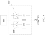
- FIG. 3 shows an ESD protection unit 130 ′ according to one embodiment of the present disclosure.
- the ESD protection unit 130 ′ can be used to replace the ESD protection units 130 A 1 to 130 AN and 130 B 1 to 130 BN in the semiconductor chip 100 .
- the ESD protection unit 130 ′ include a first ESD protection element 132 ′, a second ESD protection element 134 ′, a first fuse 136 ′ and a second fuse 138 ′.
- the first fuse 136 ′ is coupled in series with the first ESD protection element 132 ′ between an electrical contact 110 ′ and a voltage terminal VT
- the second fuse 138 ′ is coupled in series with the second ESD protection element 134 ′ between an electrical contact 110 ′ and the voltage terminal VT.
- the voltage terminal VT can be coupled to the ground GND or the power voltage VDD.
- the capacitance of the first ESD protection element 132 ′ and the capacitance of the second ESD protection element 134 ′ can be different.
- the manufacturer may decide to burn out the first fuse 136 ′ or the second fuse 138 ′ for providing the ESD protection with the desired capacitance according to customer's requirements before shipping the semiconductor chip 100 or before the semiconductor chip 100 is installed.
- the ESD protection units 130 ′ may further include more ESD protection elements and fuses so as to provide more options of capacitance.
- FIG. 4 shows a semiconductor chip 200 according to another embodiment of the present disclosure.
- the semiconductor chips 200 includes electrical contacts 2101 to 210 N, an application circuit 220 , ESD protection units 2301 to 230 N, and a control circuit 240 .
- the ESD protection unit 2301 to 230 N may have different structures from those of the ESD protection unit 130 A 1 to 130 AN and 130 B 1 to 130 BN.
- FIG. 5 shows the ESD protection unit 2301 according to one embodiment of the present disclosure.
- the ESD protection units 2301 to 230 N can have the same structures.
- the ESD protection unit 2301 includes a first ESD protection element 232 , a second ESD protection element 234 , and a switch 236 .
- the first ESD protection element 232 is coupled between the first electrical contact 2101 and the voltage terminal VT, and the second ESD protection element 234 and the switch 236 are coupled in series between the first electrical contact 2101 and the voltage terminal VT.
- the voltage terminal VT can be coupled to the ground GND or the power voltage VDD.
- the control circuit 240 can turn on or turn off the switch 236 to adjust the capacitance of the first ESD protection unit 2301 .
- the first capacitance of the first ESD protection element 232 can be the same as or different from the second capacitance of the second ESD protection element 234 .
- the ESD protection unit 2301 may further include more ESD protection elements and more switches for providing more options of capacitance.
- FIG. 6 shows an ESD protection unit 230 ′ according to another embodiment of the present disclosure.
- the ESD protection unit 230 ′ can be used to implement the ESD protection units 2301 to 230 N of the semiconductor chip 200 .
- the ESD protection unit 230 ′ includes a plurality of ESD protection elements 232 ′, and a plurality of switches 236 ′.
- Each of the ESD protection element 232 ′ is coupled in series with a switch 236 ′ between an electrical contact 210 ′ and the ground.
- the ESD protection unit 230 ′ can be adjusted to have different capacitance. That is, by including more ESD protection elements 232 ′ and switches 236 ′, it allows the ESD protection unit 230 ′ to provide more options of different capacitances.
- FIG. 7 shows a semiconductor device 30 according to one embodiment of the present disclosure.
- the semiconductor device 30 includes a first semiconductor chip 300 A and a second semiconductor chip 300 B.
- the semiconductor chips 300 A and 300 B can have the same structure.
- the first semiconductor chip 300 A includes first electrical contacts 310 A 1 to 310 AN, a first application circuit 320 A, and first ESD protection units 330 A 1 to 330 AN.
- the second semiconductor chip 300 B includes second electrical contacts 310 B 1 to 310 BN, a second application circuit 320 B, and second ESD protection units 330 B 1 to 330 BN.
- each of the first ESD protection units 330 A 1 to 330 AN can be coupled between a first electrical contact of the first electrical contacts 310 A 1 to 310 AN and the voltage terminal VT
- each of the second ESD protection units 330 B 1 to 330 BN can be coupled between a second electrical contact of the second electrical contacts 310 B 1 to 310 BN and the voltage terminal VT, where the voltage terminals VT can be coupled to the ground GND or the power voltage VDD according to the system requirements.
- the first semiconductor chip 300 A and the second semiconductor chip 300 B may include more ESD protection units so that each of the electrical contacts 310 A 1 to 310 AN and 310 B 1 to 310 B 1 can be protected by two ESD protection units, one coupled to the ground GND and another coupled the power voltage VDD, as shown in FIG. 1 .
- the first ESD protection units 330 A 1 to 330 AN and the second ESD protection units 330 B 1 to 330 BN can have the same structure as the ESD protection unit 130 A 1 or 130 B 1 shown in FIG. 2 so the capacitance of each of the first ESD protection units 330 A 1 to 330 AN is adjustable, and the capacitance of each of the second ESD protection units 330 B 1 to 330 BN is adjustable.
- each of the first electrical contacts 310 A 1 to 310 AN is coupled to a corresponding second electrical contact of the second electrical contacts 310 B 1 to 310 BN for receiving a same signal.
- the semiconductor device 30 can be a memory system
- the first application circuit 320 A and the second application circuit 320 B can be DRAM circuits that are combined to provide a wider bandwidth and a larger memory space for the semiconductor device 30 .
- the first electrical contacts 310 A 1 to 310 AN and the second electrical contacts 310 B 1 to 310 BN can be used to receive the same signals.
- the first electrical contact 310 A 1 and the second electrical contact 310 B 1 can be coupled together for receiving a signal SIGC 1 .
- the signal SIGC 1 needs to charge the equivalent capacitors or the parasitic capacitors of the first ESD protection unit 330 A 1 and the second ESD protection unit 330 B 1 before the actual voltage of the signal SIGC 1 can be sensed by the first application circuit 320 A and the second application circuit 320 B. Therefore, the signal SIGC 1 is distorted due to the capacitance of the first ESD protection unit 330 A 1 and the second ESD protection unit 330 B 1 .
- the capacitance of the first ESD protection unit 330 A 1 and the second ESD protection unit 330 B 1 can be adjusted.
- the first ESD protection unit 330 A 1 and the second ESD protection unit 330 B 1 can have the same structure as the structure of the ESD protection unit 130 A 1 shown in FIG. 2 .
- the manufacturer can burn out one of fuses in the first ESD protection unit 330 A 1 and one of fuses in the second ESD protection unit 330 B 1 , so the capacitance of each of the first ESD protection unit 330 A 1 and the second ESD protection unit 330 B 1 can be reduced.
- the first electrical contact 310 A 1 is coupled to the second electrical contact 310 B 1 , the first ESD protection unit 330 A 1 and the second ESD protection unit 330 B 1 can both be used to provide discharging paths during ESD events. Therefore, even though some of fuses in the first ESD protection unit 330 A 1 and the second ESD protection unit 330 B 1 are burned out, the remaining ESD protection elements in the first ESD protection unit 330 A 1 and the second ESD protection unit 330 B 1 can still provide sufficient protection to the first semiconductor chip 300 A and the second semiconductor chip 300 B.
- the present disclosure does not limit to implement the first ESD protection units 330 A 1 to 330 AN and the second ESD protection units 330 B 1 to 330 BN with the ESD protection unit 130 A 1 shown in FIG. 2 .
- the ESD protection unit 130 ′ shown in FIG. 3 , the ESD protection unit 2301 shown in FIG. 5 , or the ESD protection unit 230 ′ shown in FIG. 6 can be adopted to implement the first ESD protection units 330 A 1 to 330 AN and the second ESD protection units 330 B 1 to 330 BN according to system requirements.
- FIG. 8 shows a structure of the semiconductor device 30 according to one embodiment.
- the semiconductor device 30 further includes a substrate S 1 .
- the first semiconductor chip 300 A is disposed on the substrate S 1
- the second semiconductor chip 300 B is stacked on the first semiconductor chip 300 A.
- each of the second electrical contacts 310 B 1 to 310 BN can be coupled to a corresponding one of the first electrical contacts 310 A 1 to 310 AN by a through silicon via (TSV) V 1 .
- TSV through silicon via
- the second semiconductor chip 300 B may be stacked on the first semiconductor chip 300 A without covering the first electrical contacts 310 A 1 to 310 AN so the second electrical contacts 310 B 1 to 310 BN can be coupled to the first electrical contacts 310 A 1 to 310 AN by wiring bonding.
- the present disclosure does not limit the first semiconductor chip 300 A and the second semiconductor chip 300 B to be stacked.
- FIG. 9 shows a structure of the semiconductor device 30 according to another embodiment.
- the first semiconductor chip 300 A is disposed on a first surface A 1 of the substrate S 2
- the second semiconductor chip 300 B is disposed on a second surface A 2 of the substrate S 2 . That is, the first semiconductor chip 300 A and the second semiconductor chip 300 B can be disposed in a back-to-back manner.
- the second electrical contacts 310 B 1 to 310 BN can be coupled to the first electrical contacts 310 A 1 to 310 AN by conductive structures CN 1 of the substrate S 2 .
- not all the electrical contacts of the first semiconductor chip 300 A are coupled to the electrical contacts of the second semiconductor chip 300 B.
- the first semiconductor chip 300 A further includes an electrical contact 340 A and an ESD protection unit 350 A
- the second semiconductor chip 300 B further includes an electrical contact 340 B and an ESD protection unit 350 B.
- the first semiconductor chip 300 A and the second semiconductor chip 300 B can be in different ranks.
- the electrical contact 340 A can be used to receive a first semiconductor chip selection signal SIG EN1
- the electrical contact 340 B can be used to receive a second semiconductor chip selection signal SIG EN2 . That is, the electrical contact 340 A and the electrical contact 340 B are coupled to different signal sources for receiving different signals.
- the first semiconductor chip 300 A and the second semiconductor chip 300 B and be enabled according to the first semiconductor chip selection signal SIG EN1 and the second semiconductor chip selection signal SIG EN2 respectively and independently.
- each of the chip selection signals SIG EN1 and SIG EN2 needs only to charge the capacitance of the ESD protection unit 350 A or the capacitance of the ESD protection unit 350 B
- distortion of the chip selection signals SIG EN1 and SIG EN2 caused by the ESD protection unit 350 A or the capacitance of the ESD protection unit 350 B is rather predictable and acceptable. Therefore, in the present embodiment, capacitance of the ESD protection unit 350 A can be fixed and is not adjustable. Similarly, capacitance of the ESD protection unit 350 B can be fixed and is not adjustable.
- the semiconductor device 30 may further include even more semiconductor chips to further increase the memory space and/or the data bandwidth.
- FIG. 10 shows a semiconductor device 40 according to another embodiment of the present disclosure.
- the semiconductor device 40 and the semiconductor device 30 have similar structures and can be operated according to similar principles.
- the semiconductor device 40 further includes a third semiconductor chip 300 C, which has the same structure as those of the semiconductor chips 300 A and 300 B.
- the electrical contacts 310 A 1 , 310 B 1 , and 310 C 1 can be coupled together for receiving the same signal SIGC 1
- the electrical contacts 310 AN, 310 BN, and 310 CN can be coupled together for receiving the same signal SIGCN
- the signal SIGC 1 will be distorted due to the capacitance of the ESD protection units 330 A 1 , 330 B 1 , and 330 C 1 .
- the capacitance of the ESD protection units 330 A 1 , 330 B 1 , and 330 C 1 can be adjusted. For example, if the ESD protection unit 230 ′ shown in FIG. 6 is adopted to implement the ESD protection units 330 A 1 , 330 B 1 , and 330 C 1 , then for each of the ESD protection units 330 A 1 , 330 B 1 , and 330 C 1 , two of the plurality of switches 236 ′ can be turned off to reduce the capacitance.
- the ESD protection unit 230 ′ shown in FIG. 6 is adopted to implement the ESD protection units 330 A 1 and 330 B 1 in the semiconductor device 30 , one, instead of two, of the plurality of switches 236 ′ may be turned off. That is, the capacitance of the ESD protection units 230 ′ can be adjusted according to the system requirements, for example, the quantity of the semiconductor chips that are coupled together.
- FIG. 11 shows a flow chart of an ESD protection method 50 for the semiconductor device 30 .
- the method 50 includes steps S 510 to S 540 but not limited by the order below.
- the ESD protection unit 130 A 1 shown in FIG. 2 can be used to implement each of the first ESD protection units 330 A 1 to 330 AN and each of the second ESD protection units 330 B 1 to 330 BN.
- the first electrical contacts 310 A 1 to 310 AN can be coupled to the second electrical contacts 310 B 1 to 310 BN correspondingly to receive the same signals in step S 530 , and then the capacitance of the first ESD protection units 330 A 1 to 330 AN and the capacitance of each of the second ESD protection units 330 B 1 to 330 BN can be adjusted in step S 540 .
- step S 540 can be performed before step S 530 .
- the manufacturer or the user may adjust the capacitance of the first ESD protection units 330 A 1 to 330 AN and capacitance of each of the second ESD protection units 330 B 1 to 330 BN by turning off some of switches or burning out some of fuses in the ESD protection units 330 A 1 to 330 AN and 330 B 1 to 330 BN according to the design of the ESD protection units 330 A 1 to 330 AN and 330 B 1 to 330 BN.
- At least one of the ESD protection elements in the ESD protection unit 330 A 1 may be uncoupled from the first electrical contact 310 A or the voltage terminal VT, thereby reducing the capacitance of the ESD protection unit 330 A 1 .
- the semiconductor chips 300 A and 300 B can be installed to the substrate S 1 and the electrical contacts 310 A 1 to 310 AN and 310 B 1 to 310 BN can be coupled accordingly.
- the targeted capacitance of the ESD protection units 330 A 1 to 330 AN and 330 B 1 to 330 BN can be determined according to a total quantity of semiconductor chips in the semiconductor device 30 .
- the semiconductor device 30 includes two semiconductor chips 300 A and 300 B as shown in FIG. 7 while the semiconductor device 40 includes three semiconductor chips 300 A, 300 B, and 300 C as shown in FIG. 10 .
- the targeted capacitance of the ESD protection units in the three semiconductor chips 300 A, 300 B, and 300 C of the semiconductor device 40 may be smaller than the targeted capacitance of the ESD protection units in the three semiconductor chips 300 A and 300 B of the semiconductor device 30 . That is, the capacitance of the ESD protection units can be adjusted according to the system requirements, for example, the quantity of the semiconductor chips that are coupled together.
- the semiconductor chip, the semiconductor device, and the ESD protection method for the semiconductor device thereof can adjust capacitance of ESD protection units according to system requirements. Therefore, when multiple semiconductor chips are stacked or coupled to together for receiving the same signals simultaneously, the signal distortion caused by the capacitance of the ESD protection units of those semiconductor chips can be mitigated, thereby shortening the rise time and the fall time of the signals and improving the transmission quality of the signals.
Abstract
The present application discloses a semiconductor chip, a semiconductor device and an electrostatic discharge (ESD) protection method for a semiconductor device. The semiconductor chip includes an electrical contact, an application circuit, and an ESD protection unit. The application circuit performs operations according to a one signal received by the electrical contact. The ESD protection unit is coupled to the electrical contact. The capacitance of the ESD protection unit is adjustable.
Description
The present disclosure relates to a semiconductor chip, and more particularly, to a semiconductor chip including electrostatic discharge protection units of adjustable capacitance.
Electrostatic discharge (ESD) occurs when two differently-charged objects contact with each other. For example, when a pad of a semiconductor chip contacts a charged object, such as human body or a circuit board, an ESD event would occur. In such case, a drastic discharge current will be induced on the pad of the semiconductor chip so as to discharge charges accumulated in the semiconductor chip or the charged object. To protect components in the semiconductor chip from being damaged by the drastic and intensive discharge current, ESD protection circuits are often added to pads of the semiconductor chip.
However, the ESD protection circuits often include capacitive elements, which may cause distortion to signals received by the pads. For example, a rise time and a fall time of a signal will be extended because the signal has to charge or discharge the capacitive elements. Furthermore, as signals have higher frequencies, it would be even more difficult to identify the data delivered by the signals. In addition, in a multi-chip device, such as a memory device including multiple stacked dynamic random access memory (DRAM) chips, the chips of different ranks may be coupled together for receiving the same signals and operating in parallel. In such case, those signals will have to charge or discharge capacitive elements in all of the chips that coupled together, thereby further deteriorate the quality of signals.
This Discussion of the Background section is provided for background information only. The statements in this Discussion of the Background are not an admission that the subject matter disclosed in this section constitutes prior art to the present disclosure, and no part of this Discussion of the Background section may be used as an admission that any part of this application, including this Discussion of the Background section, constitutes prior art to the present disclosure.
One aspect of the present disclosure provides a semiconductor chip including an electrical contact, an application circuit, and an electrostatic discharge (ESD) protection unit. The application circuit is configured to perform operations according to at least a signal received by the electrical contact. The ESD protection unit is coupled to the electrical contact. Capacitance of the ESD protection unit is adjustable.
In some embodiments, the first ESD protection unit comprises a first ESD protection element and a second ESD protection element. The first ESD protection element is coupled between the electrical contact and a voltage terminal, and has first capacitance. The second ESD protection element is coupled between the electrical contact and the ground, and has second capacitance. The voltage terminal is coupled to a ground or a power voltage.
In some embodiments, the first ESD protection unit further comprises a switch coupled in series with the second ESD protection element between the electrical contact and the voltage terminal. The semiconductor chip further comprises a control circuit configured to turn on or turn off the switch for adjusting capacitance of the ESD protection unit.
In some embodiments, the ESD protection unit further comprises a fuse coupled in series with the second ESD protection element between the electrical contact and the voltage terminal. The fuse is configured to be burned to decrease capacitance of the ESD protection unit.
In some embodiments, the ESD protection element comprises a diode.
Another aspect of the present disclosure provides a semiconductor device. The semiconductor device comprises a first semiconductor chip and a second semiconductor chip. The first semiconductor chip comprises a first electrical contact, a first application circuit, and a first electrostatic discharge (ESD) protection unit. The first application circuit is configured to perform operations according to at least a signal received by the first electrical contact. The first ESD protection unit is coupled to the first electrical contact. The second semiconductor chip comprises a second electrical contact, a second application circuit, and a second ESD protection unit. The second application circuit is configured to perform operations according to at least a signal received by the second electrical contact. The second ESD protection unit is coupled to the second electrical contact. The first electrical contact is coupled to the second electrical contact for receiving a same signal. Capacitance of the first ESD protection unit is adjustable, and capacitance of the second ESD protection unit is adjustable.
In some embodiments, the first ESD protection unit comprises a first ESD protection element and a second ESD protection element. The first ESD protection element is coupled between the first electrical contact and a voltage terminal, and has first capacitance. The second ESD protection element is coupled between the first electrical contact and the voltage terminal, and has second capacitance. The voltage terminal is coupled to a ground or a power voltage.
In some embodiments, the first ESD protection unit further comprises a switch coupled in series with the second ESD protection element between the first electrical contact and the voltage terminal. The first semiconductor chip further comprises a control circuit configured to turn on or turn off the switch for adjusting capacitance of the first ESD protection unit.
In some embodiments, the first ESD protection unit further comprises a fuse coupled in series with the second ESD protection element between the first electrical contact and the voltage terminal, and the fuse is configured to be burned to decrease capacitance of the first ESD protection unit.
In some embodiments, the first ESD protection element comprises a diode.
In some embodiments, the first application circuit of the first semiconductor chip and the second application circuit of the second semiconductor chip are dynamic random access memory (DRAM) circuits.
In some embodiments, the semiconductor device further comprises a substrate, wherein the first semiconductor chip is disposed on the substrate, and the second semiconductor chip is stacked on the first semiconductor chip.
In some embodiments, the semiconductor device further comprises a substrate, wherein the first semiconductor chip is disposed on a first surface of the substrate, and the second semiconductor chip is disposed on a second surface of the substrate.
In some embodiments, the semiconductor device further comprises a third electrical contact and a third ESD protection unit. The third electrical contact is configured to receive a first semiconductor chip selection signal, and the third ESD protection unit is coupled between the third electrical contact and a voltage terminal. Capacitance of the third ESD protection unit is not adjustable.
In some embodiments, the semiconductor device the second semiconductor chip further comprises a fourth electrical contact and a fourth ESD protection unit. The fourth electrical contact is configured to receive a second semiconductor chip selection signal different from the first semiconductor chip selection signal, and the fourth ESD protection unit is coupled between the fourth electrical contact and the voltage terminal. Capacitance of the fourth ESD protection unit is not adjustable.
Another aspect of the present disclosure provides an electrostatic discharge (ESD) protection method for a semiconductor device. The semiconductor device comprises a first semiconductor chip and a second semiconductor chip, the first semiconductor chip comprises a first electrical contact, and the second semiconductor chip comprises a second electrical contact. The method comprises forming a first ESD protection unit in the first semiconductor chip, wherein the first ESD protection unit is coupled to the first electrical contact, forming a second ESD protection unit in the second semiconductor chip, wherein the second ESD protection unit is coupled to the second electrical contact, coupling the first electrical contact to the second electrical contact, and adjusting capacitance of the first ESD protection unit and capacitance of the second ESD protection unit.
In some embodiments, the first ESD protection unit comprises a plurality of ESD protection elements coupled between the first electrical contact and a voltage terminal. The voltage terminal is coupled to a ground or a power voltage. Adjusting the capacitance of the first ESD protection unit and the capacitance of the second ESD protection unit comprises uncoupling at least one of the plurality of ESD protection elements from the first electrical contact or the voltage terminal.
In some embodiments, the semiconductor device further comprises at least one semiconductor chip having a same structure as the first semiconductor chip and comprising an electrical contact coupled to the first electrical contact of the first semiconductor chip. The method further comprises determining targeted capacitance of the first ESD protection unit and the second ESD protection unit according to a total quantity of semiconductor chips including the first semiconductor chip, the second semiconductor chip, and the at least one semiconductor chip in the semiconductor device.
In some embodiments, each of the first semiconductor chip and the second semiconductor chip comprises dynamic random access memory circuit.
In some embodiments, the semiconductor device further comprises a substrate, the first semiconductor chip is disposed on the substrate, and the second semiconductor chip is stacked on the first semiconductor chip.
Since the semiconductor chip, the semiconductor device, and the ESD protection method for the semiconductor device thereof can adjust capacitance of ESD protection units according to system requirements, signal distortion caused by capacitance of the ESD protection units] can be mitigated.
The foregoing has outlined rather broadly the features and technical advantages of the present disclosure in order that the detailed description of the disclosure that follows may be better understood. Additional features and advantages of the disclosure will be described hereinafter, and form the subject of the claims of the disclosure. It should be appreciated by those skilled in the art that the conception and specific embodiment disclosed may be readily utilized as a basis for modifying or designing other structures or processes for carrying out the same purposes of the present disclosure. It should also be realized by those skilled in the art that such equivalent constructions do not depart from the spirit and scope of the disclosure as set forth in the appended claims.
Aspects of the present disclosure are best understood from the following detailed description when read with the accompanying figures. It should be noted that, in accordance with the standard practice in the industry, various features are not drawn to scale. In fact, the dimensions of the various features may be arbitrarily increased or reduced for clarity of discussion.
The following disclosure provides many different embodiments, or examples, for implementing different features of the provided subject matter. Specific examples of components and arrangements are described below to simplify the present disclosure. These are, of course, merely examples and are not intended to be limiting. For example, the formation of a first feature over or on a second feature in the description that follows may include embodiments in which the first and second features are formed in direct contact, and may also include embodiments in which additional features may be formed between the first and second features, such that the first and second features may not be in direct contact. In addition, the present disclosure may repeat reference numerals and/or letters in the various examples. This repetition is for the purpose of simplicity and clarity and does not in itself dictate a relationship between the various embodiments and/or configurations discussed.
Further, spatially relative terms, such as “beneath,” “below,” “lower,” “above,” “upper” and the like, may be used herein for ease of description to describe one element or feature's relationship to another element(s) or feature(s) as illustrated in the figures. The spatially relative terms are intended to encompass different orientations of the device in use or operation in addition to the orientation depicted in the figures. The apparatus may be otherwise oriented (rotated 90 degrees or at other orientations) and the spatially relative descriptors used herein may likewise be interpreted accordingly.
It will be understood that when an element or layer is referred to as being “connected to,” or “coupled to” another element or layer, it can be directly connected to or coupled to another element or layer or intervening elements or layers may be present.
It will be understood that, although the terms first, second, etc. may be used herein to describe various elements, these elements should not be limited by these terms. Unless indicated otherwise, these terms are only used to distinguish one element from another element. Thus, for example, a first element, a first component or a first section discussed below could be termed a second element, a second component or a second section without departing from the teachings of the present disclosure.
Unless the context indicates otherwise, terms such as “same,” “equal,” “planar,” or “coplanar,” as used herein when referring to orientation, layout, location, shapes, sizes, amounts, or other measures do not necessarily mean an exactly identical orientation, layout, location, shape, size, amount, or other measure, but are intended to encompass nearly identical orientation, layout, location, shapes, sizes, amounts, or other measures within acceptable variations that may occur, for example, due to manufacturing processes. The term “substantially” may be used herein to reflect this meaning. For example, items described as “substantially the same,” “substantially equal,” or “substantially planar,” may be exactly the same, equal, or planar, or may be the same, equal, or planar within acceptable variations that may occur, for example, due to manufacturing processes.
In the present disclosure, a semiconductor device generally means a device which can function by utilizing semiconductor characteristics, and an electro-optic device, a light-emitting display device, a semiconductor circuit, and a semiconductor device are all included in the category of the semiconductor device. Specifically, semiconductor devices of embodiments of the present disclosure may be dynamic random-access memory devices.
Note that, in the description of the present disclosure, above (or up) corresponds to the direction of the arrow of the direction Z, and below (or down) corresponds to the opposite direction of the arrow of the direction Z.
Each of the electrical contacts 1101 to 110N can receive a signal. In some embodiments, the electrical contacts 1101 to 110N can be pins, solder pads, micro bumps or other types of contact body for external connection. The application circuit 120 can perform operations according to signals received by the electrical contacts 1101 to 110N. For example, the application circuit 120 can be a dynamic random access memory (DRAM) circuit. In such case, some of the electrical contacts 1101 to 110N would receive read/write commands, and addresses or data corresponding to the commands, and the application circuit 120 would perform read operations or write operations according to the commands, and transmit the requested data through some of the electrical contacts 1101 to 110N.
Since the electrical contacts 1101 to 110N are used for external connection, ESD protection units 130A1 to 130AN and 130B1 to 130BN are coupled to the electrical contacts 1101 to 110N for providing discharge paths at the electrical contacts 1101 to 110N, thereby preventing the discharge currents from damaging the application circuit 120. As shown in FIG. 1 , each of the ESD protection units 130A1 to 130AN and 130B1 to 130BN is coupled to a corresponding electrical contact of the electrical contacts 1101 to 110N. For example, the ESD protection unit 130A1 is coupled to the electrical contact 1101, and the ESD protection unit 130AN is coupled to the electrical contact 110N. Furthermore, in the present embodiment, capacitance of the ESD protection units 130A1 to 130AN and 130B1 to 130BN is adjustable. That is, capacitance of each of the ESD protection units 130A1 to 130AN and 130B1 to 130BN can be adjusted according to system requirements.
The first ESD protection element 132A is coupled between the first electrical contact 1101 and the ground GND, and the second ESD protection element 134A is also coupled between the first electrical contact 1101 and the ground GND. The first ESD protection element 132A has first capacitance, and the second ESD protection element 134A has second capacitance.
Since the first ESD protection element 132A and the second ESD protection element 134A are coupled in parallel between the first electrical contact 1101 and the ground GND, the equivalent capacitance of the ESD protection unit 130A1 is substantially the sum of the first capacitance of the first ESD protection element 132A and the second capacitance of the second ESD protection element 134A. In the present embodiment, to allow the ESD protection unit 130A1 to have adjustable capacitance, the ESD protection unit 130A1 further includes a fuse 136A coupled in series with the second ESD protection element 134A between the first electrical contact 1101 and the ground GND. In such case, the fuse 136A can be burned out to uncouple the second ESD protection element 134A from the first electrical contact 1101 or the ground GND, so the second ESD protection element 134A will no longer be able to provide discharge paths between the first electrical contact 1101 and the ground GND, and the capacitance of the first ESD protection unit 130A1 is decreased. That is, the capacitance of the first ESD protection unit 130A1 can be adjusted by burning out the fuse 136A according to system requirements. In some embodiments, the semiconductor chip 100 may further include other circuits or components (not shown in FIG. 2 ) for controlling the fuse 136A so that the fuse 136A can be burned without damaging other components in the semiconductor chip 100.
As shown in FIG. 2 , the first ESD protection element 132A includes a diode D1A. The diode D1A has an anode coupled to the ground GND, and a cathode coupled to the first electrical contact 1101. Similarly, the second ESD protection element 134A also includes a diode D2A having an anode coupled to the ground GND, and a cathode coupled to the first electrical contact 1101. As a result, when the voltage at the first electrical contact 1101 is raised drastically during the ESD event, the diodes D1A and/or D2A can be broken down and thus provide discharging paths for ESD currents. In some embodiments, the diodes D1A and D2A may have the same sizes. In such case, the first capacitance of the first ESD protection element 132A can be substantially equal to the second capacitance of the second ESD protection element 134A. However, the present disclosure is not limited thereto. In some other embodiments, the diodes D1A and D2A may have different sizes, and the first capacitance of the first ESD protection element 132A can be different from the second capacitance of the second ESD protection element 134A. Furthermore, in some other embodiments, the first ESD protection element 132A and the second ESD protection element 134A may include diodes, capacitors, resistors, and/or transistors.
Similarly, the ESD protection unit 130B1 includes a first ESD protection element 132B, a second ESD protection element 134B, and a fuse 136B. However, the ESD protection unit 130B1 can be coupled between the first electrical contact 1101 and a power voltage VDD. That is, the ESD protection unit 130B1 can be used to provide another discharge path to the power voltage VDD for ESD protection. In such case, the diode D1B of the first ESD protection element 132B has an anode coupled to the first electrical contact 1101, and a cathode coupled to the power voltage VDD. Similarly, the diode D2B of the second ESD protection element 134B has an anode coupled to the first electrical contact 1101, and a cathode coupled to the power voltage VDD. As a result, if the voltage at the first electrical contact is pulled down drastically during the ESD event, the diodes D1B and/or D2B will be broken down and thus provide discharging paths for ESD currents. That is, the ESD protection units 130A1 to 130AN can be used to provide discharging path to the ground GND, and the ESD protection units 130B1 to 130BN can be used to provide discharging path to the power voltage VDD. However, the present disclosure is not limited thereto. In some other embodiments, the semiconductor chip 100 may omit some of the ESD protection units 130A1 to 130AN and 130B1 to 130BN according to system requirements. For example, in some embodiments, the semiconductor chip 100 may include the ESD protection units 130A1 to 130AN and omit the ESD protection units 130B1 to 130BN if the ESD events on the power voltage VDD can be ignored.
The first ESD protection element 232 is coupled between the first electrical contact 2101 and the voltage terminal VT, and the second ESD protection element 234 and the switch 236 are coupled in series between the first electrical contact 2101 and the voltage terminal VT. The voltage terminal VT can be coupled to the ground GND or the power voltage VDD. In such case, the control circuit 240 can turn on or turn off the switch 236 to adjust the capacitance of the first ESD protection unit 2301. Furthermore, the first capacitance of the first ESD protection element 232 can be the same as or different from the second capacitance of the second ESD protection element 234. In addition, in some embodiments, the ESD protection unit 2301 may further include more ESD protection elements and more switches for providing more options of capacitance.
In the present embodiment, the first ESD protection units 330A1 to 330AN and the second ESD protection units 330B1 to 330BN can have the same structure as the ESD protection unit 130A1 or 130B1 shown in FIG. 2 so the capacitance of each of the first ESD protection units 330A1 to 330AN is adjustable, and the capacitance of each of the second ESD protection units 330B1 to 330BN is adjustable.
Furthermore, as shown in FIG. 7 , each of the first electrical contacts 310A1 to 310AN is coupled to a corresponding second electrical contact of the second electrical contacts 310B1 to 310BN for receiving a same signal. For example, the semiconductor device 30 can be a memory system, and the first application circuit 320A and the second application circuit 320B can be DRAM circuits that are combined to provide a wider bandwidth and a larger memory space for the semiconductor device 30. In such case, the first electrical contacts 310A1 to 310AN and the second electrical contacts 310B1 to 310BN can be used to receive the same signals. For example, the first electrical contact 310A1 and the second electrical contact 310B1 can be coupled together for receiving a signal SIGC1. However, since the first ESD protection unit 330A1 and the second ESD protection unit 330B1 are capacitive, the signal SIGC1 needs to charge the equivalent capacitors or the parasitic capacitors of the first ESD protection unit 330A1 and the second ESD protection unit 330B1 before the actual voltage of the signal SIGC1 can be sensed by the first application circuit 320A and the second application circuit 320B. Therefore, the signal SIGC1 is distorted due to the capacitance of the first ESD protection unit 330A1 and the second ESD protection unit 330B1.
To mitigate the distortion of the signal SIGC1, the capacitance of the first ESD protection unit 330A1 and the second ESD protection unit 330B1 can be adjusted. For example, the first ESD protection unit 330A1 and the second ESD protection unit 330B1 can have the same structure as the structure of the ESD protection unit 130A1 shown in FIG. 2 . In such case, the manufacturer can burn out one of fuses in the first ESD protection unit 330A1 and one of fuses in the second ESD protection unit 330B1, so the capacitance of each of the first ESD protection unit 330A1 and the second ESD protection unit 330B1 can be reduced. Furthermore, since the first electrical contact 310A1 is coupled to the second electrical contact 310B1, the first ESD protection unit 330A1 and the second ESD protection unit 330B1 can both be used to provide discharging paths during ESD events. Therefore, even though some of fuses in the first ESD protection unit 330A1 and the second ESD protection unit 330B1 are burned out, the remaining ESD protection elements in the first ESD protection unit 330A1 and the second ESD protection unit 330B1 can still provide sufficient protection to the first semiconductor chip 300A and the second semiconductor chip 300B. However, the present disclosure does not limit to implement the first ESD protection units 330A1 to 330AN and the second ESD protection units 330B1 to 330BN with the ESD protection unit 130A1 shown in FIG. 2 . In some other embodiments, the ESD protection unit 130′ shown in FIG. 3 , the ESD protection unit 2301 shown in FIG. 5 , or the ESD protection unit 230′ shown in FIG. 6 can be adopted to implement the first ESD protection units 330A1 to 330AN and the second ESD protection units 330B1 to 330BN according to system requirements.
In some embodiments, not all the electrical contacts of the first semiconductor chip 300A are coupled to the electrical contacts of the second semiconductor chip 300B. For example, as shown in FIG. 7 , the first semiconductor chip 300A further includes an electrical contact 340A and an ESD protection unit 350A, and the second semiconductor chip 300B further includes an electrical contact 340B and an ESD protection unit 350B. For example, the first semiconductor chip 300A and the second semiconductor chip 300B can be in different ranks. In such case, the electrical contact 340A can be used to receive a first semiconductor chip selection signal SIGEN1, and the electrical contact 340B can be used to receive a second semiconductor chip selection signal SIGEN2. That is, the electrical contact 340A and the electrical contact 340B are coupled to different signal sources for receiving different signals. Therefore, the first semiconductor chip 300A and the second semiconductor chip 300B and be enabled according to the first semiconductor chip selection signal SIGEN1 and the second semiconductor chip selection signal SIGEN2 respectively and independently. In such case, since each of the chip selection signals SIGEN1 and SIGEN2 needs only to charge the capacitance of the ESD protection unit 350A or the capacitance of the ESD protection unit 350B, distortion of the chip selection signals SIGEN1 and SIGEN2 caused by the ESD protection unit 350A or the capacitance of the ESD protection unit 350B is rather predictable and acceptable. Therefore, in the present embodiment, capacitance of the ESD protection unit 350A can be fixed and is not adjustable. Similarly, capacitance of the ESD protection unit 350B can be fixed and is not adjustable.
In some embodiments, the semiconductor device 30 may further include even more semiconductor chips to further increase the memory space and/or the data bandwidth. FIG. 10 shows a semiconductor device 40 according to another embodiment of the present disclosure. The semiconductor device 40 and the semiconductor device 30 have similar structures and can be operated according to similar principles. However, the semiconductor device 40 further includes a third semiconductor chip 300C, which has the same structure as those of the semiconductor chips 300A and 300B. In such case, if a signal is transmitted to the three semiconductor chips 300A, 300B, and 300C, then such signal will have to charge the equivalent capacitors or the parasitic capacitors of the ESD protection units of the three semiconductor chips 300A, 300B, and 300C before the actual voltage of such signal can be sensed by the application circuits 320A, 320B, and 320C of the three semiconductor chips 300A, 300B, and 300C.
For example, as shown in FIG. 10 , the electrical contacts 310A1, 310B1, and 310C1 can be coupled together for receiving the same signal SIGC1, and the electrical contacts 310AN, 310BN, and 310CN can be coupled together for receiving the same signal SIGCN In such case, the signal SIGC1 will be distorted due to the capacitance of the ESD protection units 330A1, 330B1, and 330C1. To prevent the signals from being distorted by the ESD protection units 330A1, 330B1, and 330C1 coupled to the electrical contacts 310A1, 310B1, and 310C1, the capacitance of the ESD protection units 330A 1, 330B1, and 330C1 can be adjusted. For example, if the ESD protection unit 230′ shown in FIG. 6 is adopted to implement the ESD protection units 330A1, 330B1, and 330C1, then for each of the ESD protection units 330A1, 330B1, and 330C1, two of the plurality of switches 236′ can be turned off to reduce the capacitance. However, in some embodiments, if the ESD protection unit 230′ shown in FIG. 6 is adopted to implement the ESD protection units 330A1 and 330B1 in the semiconductor device 30, one, instead of two, of the plurality of switches 236′ may be turned off. That is, the capacitance of the ESD protection units 230′ can be adjusted according to the system requirements, for example, the quantity of the semiconductor chips that are coupled together.
S510: form the first ESD protection units 330A1 to 330AN in the first semiconductor 300A;
S520: form the second ESD protection units 330B1 to 330BN in the second semiconductor 300B;
S530: couple each of the first electrical contacts 310A1 to 310AN to a corresponding second electrical contact of the second electrical contacts 310B1 to 310BN; and
S540: adjust capacitance of the first ESD protection units 330A1 to 330AN and capacitance of each of the second ESD protection units 330B1 to 330BN.
In steps S510 and S520, the ESD protection unit 130A1 shown in FIG. 2 , the ESD protection unit 130′ shown in FIG. 3 , the ESD protection unit 2301 shown in FIG. 5 , or the ESD protection unit 230′ shown in FIG. 6 can be used to implement each of the first ESD protection units 330A1 to 330AN and each of the second ESD protection units 330B1 to 330BN.
In the present embodiment, the first electrical contacts 310A1 to 310AN can be coupled to the second electrical contacts 310B1 to 310BN correspondingly to receive the same signals in step S530, and then the capacitance of the first ESD protection units 330A1 to 330AN and the capacitance of each of the second ESD protection units 330B1 to 330BN can be adjusted in step S540. However, in some embodiments, step S540 can be performed before step S530. For example, if the manufacturer or the user has already known that there will be two semiconductor chips 300A and 300B in the semiconductor device 30 in an early stage, then the manufacturer or the user may adjust the capacitance of the first ESD protection units 330A1 to 330AN and capacitance of each of the second ESD protection units 330B1 to 330BN by turning off some of switches or burning out some of fuses in the ESD protection units 330A1 to 330AN and 330B1 to 330BN according to the design of the ESD protection units 330A1 to 330AN and 330B1 to 330BN. For example, at least one of the ESD protection elements in the ESD protection unit 330A1 may be uncoupled from the first electrical contact 310A or the voltage terminal VT, thereby reducing the capacitance of the ESD protection unit 330A1. Afterwards, the semiconductor chips 300A and 300B can be installed to the substrate S1 and the electrical contacts 310A1 to 310AN and 310B1 to 310BN can be coupled accordingly.
Furthermore, in some embodiments, the targeted capacitance of the ESD protection units 330A 1 to 330AN and 330B1 to 330BN can be determined according to a total quantity of semiconductor chips in the semiconductor device 30. For example, the semiconductor device 30 includes two semiconductor chips 300A and 300B as shown in FIG. 7 while the semiconductor device 40 includes three semiconductor chips 300A, 300B, and 300C as shown in FIG. 10 . In such cases, the targeted capacitance of the ESD protection units in the three semiconductor chips 300A, 300B, and 300C of the semiconductor device 40 may be smaller than the targeted capacitance of the ESD protection units in the three semiconductor chips 300A and 300B of the semiconductor device 30. That is, the capacitance of the ESD protection units can be adjusted according to the system requirements, for example, the quantity of the semiconductor chips that are coupled together.
In summary, the semiconductor chip, the semiconductor device, and the ESD protection method for the semiconductor device thereof can adjust capacitance of ESD protection units according to system requirements. Therefore, when multiple semiconductor chips are stacked or coupled to together for receiving the same signals simultaneously, the signal distortion caused by the capacitance of the ESD protection units of those semiconductor chips can be mitigated, thereby shortening the rise time and the fall time of the signals and improving the transmission quality of the signals.
Although the present disclosure and its advantages have been described in detail, it should be understood that various changes, substitutions and alterations can be made herein without departing from the spirit and scope of the disclosure as defined by the appended claims. For example, many of the processes discussed above can be implemented in different methodologies and replaced by other processes, or a combination thereof.
Moreover, the scope of the present application is not intended to be limited to the particular embodiments of the process, machine, manufacture, composition of matter, means, methods and steps described in the specification. As one of ordinary skill in the art will readily appreciate from the disclosure of the present disclosure, processes, machines, manufacture, compositions of matter, means, methods, or steps, presently existing or later to be developed, that perform substantially the same function or achieve substantially the same result as the corresponding embodiments described herein may be utilized according to the present disclosure. Accordingly, the appended claims are intended to include within their scope such processes, machines, manufacture, compositions of matter, means, methods, and steps.
Claims (18)
1. A semiconductor chip, comprising:
an electrical contact;
an application circuit configured to perform operations according to at least a signal received by the electrical contact; and
an electrostatic discharge (ESD) protection unit coupled to the electrical contact;
wherein capacitance of the ESD protection unit is adjustable;
wherein the ESD protection unit comprises:
a first ESD protection element coupled between the electrical contact and a voltage terminal, and having first capacitance;
a second ESD protection element coupled between the electrical contact and the voltage terminal, and having second capacitance;
wherein the voltage terminal is coupled to a ground or a power voltage;
wherein:
the ESD protection unit further comprises a switch coupled in series with the second ESD protection element between the electrical contact and the voltage terminal; and
the semiconductor chip further comprises a control circuit configured to turn on or turn off the switch for adjusting capacitance of the ESD protection unit.
2. The semiconductor chip of claim 1 , wherein:
the ESD protection unit further comprises a fuse coupled in series with the second ESD protection element between the electrical contact and the voltage terminal; and
the fuse is configured to be burned to decrease capacitance of the ESD protection unit.
3. The semiconductor chip of claim 1 , wherein the ESD protection element comprises a diode.
4. A semiconductor device comprising:
a first semiconductor chip comprising:
a first electrical contact;
a first application circuit configured to perform operations according to at least a signal received by the first electrical contact; and
a first electrostatic discharge (ESD) protection unit coupled to the first electrical contact; and
a second semiconductor chip comprising:
a second electrical contact;
a second application circuit configured to perform operations according to at least a signal received by the second electrical contact; and
a second ESD protection unit coupled to the second electrical contact;
wherein:
the first electrical contact is coupled to the second electrical contact for receiving a same signal;
capacitance of the first ESD protection unit is adjustable; and
capacitance of the second ESD protection unit is adjustable.
5. The semiconductor device of claim 4 , wherein the first ESD protection unit comprises:
a first ESD protection element coupled between the first electrical contact and a voltage terminal, and having first capacitance; and
a second ESD protection element coupled between the first electrical contact and the voltage terminal, and having second capacitance;
wherein the voltage terminal is coupled to a ground or a power voltage.
6. The semiconductor device of claim 5 , wherein:
the first ESD protection unit further comprises a switch coupled in series with the second ESD protection element between the first electrical contact and the voltage terminal; and
the first semiconductor chip further comprises a control circuit configured to turn on or turn off the switch for adjusting capacitance of the first ESD protection unit.
7. The semiconductor device of claim 5 , wherein:
the first ESD protection unit further comprises a fuse coupled in series with the second ESD protection element between the first electrical contact and the voltage terminal; and
the fuse is configured to be burned to decrease capacitance of the first ESD protection unit.
8. The semiconductor device of claim 5 , wherein the first ESD protection element comprises a diode.
9. The semiconductor device of claim 4 , wherein the first application circuit of the first semiconductor chip and the second application circuit of the second semiconductor chip are dynamic random access memory (DRAM) circuits.
10. The semiconductor device of claim 4 , further comprising a substrate, wherein the first semiconductor chip is disposed on the substrate, and the second semiconductor chip is stacked on the first semiconductor chip.
11. The semiconductor device of claim 4 , further comprising a substrate, wherein the first semiconductor chip is disposed on a first surface of the substrate, and the second semiconductor chip is disposed on a second surface of the substrate.
12. The semiconductor device of claim 4 , wherein the first semiconductor chip further comprises:
a third electrical contact configured to receive a first semiconductor chip selection signal; and
a third ESD protection unit coupled between the third electrical contact and a voltage terminal;
wherein capacitance of the third ESD protection unit is not adjustable.
13. The semiconductor device of claim 12 , wherein the second semiconductor chip further comprises:
a fourth electrical contact configured to receive a second semiconductor chip selection signal different from the first semiconductor chip selection signal; and
a fourth ESD protection unit coupled between the fourth electrical contact and the voltage terminal;
wherein capacitance of the fourth ESD protection unit is not adjustable.
14. An electrostatic discharge (ESD) protection method for a semiconductor device, the semiconductor device comprising a first semiconductor chip and a second semiconductor chip, the first semiconductor chip comprising a first electrical contact, the second semiconductor chip comprising a second electrical contact, and the method comprising:
forming a first ESD protection unit in the first semiconductor chip, wherein the first ESD protection unit is coupled to the first electrical contact;
forming a second ESD protection unit in the second semiconductor chip, wherein the second ESD protection unit is coupled to the second electrical contact;
coupling the first electrical contact to the second electrical contact; and
adjusting capacitance of the first ESD protection unit and capacitance of the second ESD protection unit.
15. The method of claim 14 , wherein the first ESD protection unit comprises a plurality of ESD protection elements coupled between the first electrical contact and a voltage terminal, the voltage terminal is coupled to a ground or a power voltage, and adjusting the capacitance of the first ESD protection unit and the capacitance of the second ESD protection unit comprises:
uncoupling at least one of the plurality of ESD protection elements from the first electrical contact or the voltage terminal.
16. The method of claim 14 , wherein the semiconductor device further comprises at least one semiconductor chip having a same structure as the first semiconductor chip and comprising an electrical contact coupled to the first electrical contact of the first semiconductor chip, and the method further comprises:
determining targeted capacitance of the first ESD protection unit and the second ESD protection unit according to a total quantity of semiconductor chips including the first semiconductor chip, the second semiconductor chip, and the at least one semiconductor chip in the semiconductor device.
17. The method of claim 14 , wherein each of the first semiconductor chip and the second semiconductor chip comprises dynamic random access memory circuit.
18. The method of claim 14 , wherein the semiconductor device further comprises a substrate, the first semiconductor chip is disposed on the substrate, and the second semiconductor chip is stacked on the first semiconductor chip.
Priority Applications (3)
| Application Number | Priority Date | Filing Date | Title |
|---|---|---|---|
| US17/382,751 US11715706B2 (en) | 2021-07-22 | 2021-07-22 | Semiconductor chip, semiconductor device and electrostatic discharge protection method for semiconductor device thereof |
| TW110139350A TWI786899B (en) | 2021-07-22 | 2021-10-22 | Semiconductor device and electrostatic discharge protection method for semiconductor device thereof |
| CN202210292390.9A CN115692381A (en) | 2021-07-22 | 2022-03-23 | Semiconductor chip, semiconductor element and semiconductor element electrostatic discharge protection method |
Applications Claiming Priority (1)
| Application Number | Priority Date | Filing Date | Title |
|---|---|---|---|
| US17/382,751 US11715706B2 (en) | 2021-07-22 | 2021-07-22 | Semiconductor chip, semiconductor device and electrostatic discharge protection method for semiconductor device thereof |
Publications (2)
| Publication Number | Publication Date |
|---|---|
| US20230028109A1 US20230028109A1 (en) | 2023-01-26 |
| US11715706B2 true US11715706B2 (en) | 2023-08-01 |
Family
ID=84976068
Family Applications (1)
| Application Number | Title | Priority Date | Filing Date |
|---|---|---|---|
| US17/382,751 Active 2041-12-03 US11715706B2 (en) | 2021-07-22 | 2021-07-22 | Semiconductor chip, semiconductor device and electrostatic discharge protection method for semiconductor device thereof |
Country Status (3)
| Country | Link |
|---|---|
| US (1) | US11715706B2 (en) |
| CN (1) | CN115692381A (en) |
| TW (1) | TWI786899B (en) |
Citations (10)
| Publication number | Priority date | Publication date | Assignee | Title |
|---|---|---|---|---|
| US20050029596A1 (en) * | 2003-08-06 | 2005-02-10 | Vladimir Rodov | Method and apparatus for preventing microcircuit thermo-mechanical damage during an ESD event |
| US20120236444A1 (en) | 2011-03-14 | 2012-09-20 | Qualcomm Incorporated | Charge pump electrostatic discharge protection |
| US8878304B2 (en) | 2011-11-04 | 2014-11-04 | Richtek Technology Corporation, R.O.C. | Fuse circuit for final test trimming of integrated circuit chip |
| US20150188312A1 (en) | 2013-12-27 | 2015-07-02 | Cambridge Silicon Radio Limited | Electrostatic discharge protection |
| TW201628160A (en) | 2015-01-20 | 2016-08-01 | 台灣積體電路製造股份有限公司 | Electro-static discharge structure, circuit including the same and method of using the same |
| US20180139826A1 (en) * | 2015-05-07 | 2018-05-17 | Moda-Innochips Co., Ltd. | Electric shock-prevention element and electronic device provided with same |
| TW201840087A (en) | 2017-04-27 | 2018-11-01 | 力旺電子股份有限公司 | Electro static discharge circuit |
| TW202005041A (en) | 2018-06-04 | 2020-01-16 | 茂達電子股份有限公司 | ESD protection circuit |
| US20200219828A1 (en) * | 2019-01-07 | 2020-07-09 | Credo Technology Group Limited | Compensation Network for High Speed Integrated Circuits |
| TW202119722A (en) | 2019-11-01 | 2021-05-16 | 立積電子股份有限公司 | Integrated circuit with electrostatic discharge protection |
-
2021
- 2021-07-22 US US17/382,751 patent/US11715706B2/en active Active
- 2021-10-22 TW TW110139350A patent/TWI786899B/en active
-
2022
- 2022-03-23 CN CN202210292390.9A patent/CN115692381A/en active Pending
Patent Citations (10)
| Publication number | Priority date | Publication date | Assignee | Title |
|---|---|---|---|---|
| US20050029596A1 (en) * | 2003-08-06 | 2005-02-10 | Vladimir Rodov | Method and apparatus for preventing microcircuit thermo-mechanical damage during an ESD event |
| US20120236444A1 (en) | 2011-03-14 | 2012-09-20 | Qualcomm Incorporated | Charge pump electrostatic discharge protection |
| US8878304B2 (en) | 2011-11-04 | 2014-11-04 | Richtek Technology Corporation, R.O.C. | Fuse circuit for final test trimming of integrated circuit chip |
| US20150188312A1 (en) | 2013-12-27 | 2015-07-02 | Cambridge Silicon Radio Limited | Electrostatic discharge protection |
| TW201628160A (en) | 2015-01-20 | 2016-08-01 | 台灣積體電路製造股份有限公司 | Electro-static discharge structure, circuit including the same and method of using the same |
| US20180139826A1 (en) * | 2015-05-07 | 2018-05-17 | Moda-Innochips Co., Ltd. | Electric shock-prevention element and electronic device provided with same |
| TW201840087A (en) | 2017-04-27 | 2018-11-01 | 力旺電子股份有限公司 | Electro static discharge circuit |
| TW202005041A (en) | 2018-06-04 | 2020-01-16 | 茂達電子股份有限公司 | ESD protection circuit |
| US20200219828A1 (en) * | 2019-01-07 | 2020-07-09 | Credo Technology Group Limited | Compensation Network for High Speed Integrated Circuits |
| TW202119722A (en) | 2019-11-01 | 2021-05-16 | 立積電子股份有限公司 | Integrated circuit with electrostatic discharge protection |
Also Published As
| Publication number | Publication date |
|---|---|
| TW202306098A (en) | 2023-02-01 |
| CN115692381A (en) | 2023-02-03 |
| TWI786899B (en) | 2022-12-11 |
| US20230028109A1 (en) | 2023-01-26 |
Similar Documents
| Publication | Publication Date | Title |
|---|---|---|
| US9184130B2 (en) | Electrostatic protection for stacked multi-chip integrated circuits | |
| US8604626B2 (en) | Reduced susceptibility to electrostatic discharge during 3D semiconductor device bonding and assembly | |
| US10418346B1 (en) | Package including a plurality of stacked semiconductor devices having area efficient ESD protection | |
| US10381334B2 (en) | Semiconductor package and method of manufacturing the semiconductor package | |
| US9853446B2 (en) | Integrated circuit (IC) package comprising electrostatic discharge (ESD) protection | |
| TW538519B (en) | An integrated circuit including esd circuits for a multi-chip module and a method therefor | |
| US20090097175A1 (en) | Esd protection substrate and integrated circuit utilizing the same | |
| US9224702B2 (en) | Three-dimension (3D) integrated circuit (IC) package | |
| US11715706B2 (en) | Semiconductor chip, semiconductor device and electrostatic discharge protection method for semiconductor device thereof | |
| US11699900B2 (en) | Semiconductor chip, electronic device and electrostatic discharge protection method for electronic device thereof | |
| US11695003B2 (en) | Semiconductor device, electronic system, and electrostatic discharge protection method for semiconductor device thereof | |
| JP4258205B2 (en) | Semiconductor device | |
| TWI804046B (en) | Display controller and display system thereof | |
| US7193314B2 (en) | Semiconductor devices and substrates used in thereof | |
| US7974054B2 (en) | Integrated circuit with electrostatic discharge protection circuit |
Legal Events
| Date | Code | Title | Description |
|---|---|---|---|
| FEPP | Fee payment procedure |
Free format text: ENTITY STATUS SET TO UNDISCOUNTED (ORIGINAL EVENT CODE: BIG.); ENTITY STATUS OF PATENT OWNER: LARGE ENTITY |
|
| AS | Assignment |
Owner name: NANYA TECHNOLOGY CORPORATION,, TAIWAN Free format text: ASSIGNMENT OF ASSIGNORS INTEREST;ASSIGNOR:LEE, CHUN-LU;REEL/FRAME:057017/0805 Effective date: 20210623 |
|
| STPP | Information on status: patent application and granting procedure in general |
Free format text: DOCKETED NEW CASE - READY FOR EXAMINATION |
|
| STPP | Information on status: patent application and granting procedure in general |
Free format text: PUBLICATIONS -- ISSUE FEE PAYMENT VERIFIED |
|
| STCF | Information on status: patent grant |
Free format text: PATENTED CASE |