US11714101B2 - Inertial sensor, electronic apparatus, and vehicle - Google Patents
Inertial sensor, electronic apparatus, and vehicle Download PDFInfo
- Publication number
- US11714101B2 US11714101B2 US16/802,137 US202016802137A US11714101B2 US 11714101 B2 US11714101 B2 US 11714101B2 US 202016802137 A US202016802137 A US 202016802137A US 11714101 B2 US11714101 B2 US 11714101B2
- Authority
- US
- United States
- Prior art keywords
- inertial sensor
- sensor element
- detection signal
- terminals
- signal terminal
- Prior art date
- Legal status (The legal status is an assumption and is not a legal conclusion. Google has not performed a legal analysis and makes no representation as to the accuracy of the status listed.)
- Active, expires
Links
- 238000001514 detection method Methods 0.000 claims abstract description 236
- 239000000758 substrate Substances 0.000 claims abstract description 99
- 230000001133 acceleration Effects 0.000 claims description 59
- 238000007689 inspection Methods 0.000 claims description 36
- 239000000463 material Substances 0.000 claims description 16
- 229910052751 metal Inorganic materials 0.000 claims description 5
- 239000002184 metal Substances 0.000 claims description 5
- 238000005259 measurement Methods 0.000 description 19
- 230000008859 change Effects 0.000 description 17
- 230000003071 parasitic effect Effects 0.000 description 16
- 230000004308 accommodation Effects 0.000 description 12
- 230000000694 effects Effects 0.000 description 12
- 238000000034 method Methods 0.000 description 9
- XUIMIQQOPSSXEZ-UHFFFAOYSA-N Silicon Chemical compound [Si] XUIMIQQOPSSXEZ-UHFFFAOYSA-N 0.000 description 8
- 230000008878 coupling Effects 0.000 description 8
- 238000010168 coupling process Methods 0.000 description 8
- 238000005859 coupling reaction Methods 0.000 description 8
- 229910052710 silicon Inorganic materials 0.000 description 8
- 239000010703 silicon Substances 0.000 description 8
- 239000002585 base Substances 0.000 description 7
- 230000015556 catabolic process Effects 0.000 description 7
- 238000006731 degradation reaction Methods 0.000 description 7
- 239000011521 glass Substances 0.000 description 7
- 238000012545 processing Methods 0.000 description 7
- 239000000470 constituent Substances 0.000 description 6
- 230000015572 biosynthetic process Effects 0.000 description 4
- 238000010586 diagram Methods 0.000 description 4
- 238000000059 patterning Methods 0.000 description 4
- 238000003786 synthesis reaction Methods 0.000 description 4
- 238000009623 Bosch process Methods 0.000 description 3
- PXHVJJICTQNCMI-UHFFFAOYSA-N Nickel Chemical compound [Ni] PXHVJJICTQNCMI-UHFFFAOYSA-N 0.000 description 3
- KDLHZDBZIXYQEI-UHFFFAOYSA-N Palladium Chemical compound [Pd] KDLHZDBZIXYQEI-UHFFFAOYSA-N 0.000 description 3
- 239000007769 metal material Substances 0.000 description 3
- BASFCYQUMIYNBI-UHFFFAOYSA-N platinum Chemical compound [Pt] BASFCYQUMIYNBI-UHFFFAOYSA-N 0.000 description 3
- XKRFYHLGVUSROY-UHFFFAOYSA-N Argon Chemical compound [Ar] XKRFYHLGVUSROY-UHFFFAOYSA-N 0.000 description 2
- IJGRMHOSHXDMSA-UHFFFAOYSA-N Atomic nitrogen Chemical compound N#N IJGRMHOSHXDMSA-UHFFFAOYSA-N 0.000 description 2
- ZOXJGFHDIHLPTG-UHFFFAOYSA-N Boron Chemical compound [B] ZOXJGFHDIHLPTG-UHFFFAOYSA-N 0.000 description 2
- OAICVXFJPJFONN-UHFFFAOYSA-N Phosphorus Chemical compound [P] OAICVXFJPJFONN-UHFFFAOYSA-N 0.000 description 2
- 239000000956 alloy Substances 0.000 description 2
- 229910045601 alloy Inorganic materials 0.000 description 2
- 229910052782 aluminium Inorganic materials 0.000 description 2
- XAGFODPZIPBFFR-UHFFFAOYSA-N aluminium Chemical compound [Al] XAGFODPZIPBFFR-UHFFFAOYSA-N 0.000 description 2
- 229910052785 arsenic Inorganic materials 0.000 description 2
- RQNWIZPPADIBDY-UHFFFAOYSA-N arsenic atom Chemical compound [As] RQNWIZPPADIBDY-UHFFFAOYSA-N 0.000 description 2
- 229910052796 boron Inorganic materials 0.000 description 2
- 239000000919 ceramic Substances 0.000 description 2
- 239000011651 chromium Substances 0.000 description 2
- 238000004891 communication Methods 0.000 description 2
- 239000010949 copper Substances 0.000 description 2
- 238000013461 design Methods 0.000 description 2
- 238000005530 etching Methods 0.000 description 2
- 239000010931 gold Substances 0.000 description 2
- 239000012535 impurity Substances 0.000 description 2
- 230000001788 irregular Effects 0.000 description 2
- 229910052698 phosphorus Inorganic materials 0.000 description 2
- 239000011574 phosphorus Substances 0.000 description 2
- 239000010936 titanium Substances 0.000 description 2
- RZVAJINKPMORJF-UHFFFAOYSA-N Acetaminophen Chemical compound CC(=O)NC1=CC=C(O)C=C1 RZVAJINKPMORJF-UHFFFAOYSA-N 0.000 description 1
- 241000251468 Actinopterygii Species 0.000 description 1
- VYZAMTAEIAYCRO-UHFFFAOYSA-N Chromium Chemical compound [Cr] VYZAMTAEIAYCRO-UHFFFAOYSA-N 0.000 description 1
- RYGMFSIKBFXOCR-UHFFFAOYSA-N Copper Chemical compound [Cu] RYGMFSIKBFXOCR-UHFFFAOYSA-N 0.000 description 1
- BQCADISMDOOEFD-UHFFFAOYSA-N Silver Chemical compound [Ag] BQCADISMDOOEFD-UHFFFAOYSA-N 0.000 description 1
- RTAQQCXQSZGOHL-UHFFFAOYSA-N Titanium Chemical compound [Ti] RTAQQCXQSZGOHL-UHFFFAOYSA-N 0.000 description 1
- 239000000853 adhesive Substances 0.000 description 1
- 230000001070 adhesive effect Effects 0.000 description 1
- 230000002411 adverse Effects 0.000 description 1
- 229910001413 alkali metal ion Inorganic materials 0.000 description 1
- 229910052786 argon Inorganic materials 0.000 description 1
- 239000005388 borosilicate glass Substances 0.000 description 1
- 238000006243 chemical reaction Methods 0.000 description 1
- 229910052804 chromium Inorganic materials 0.000 description 1
- 229910052802 copper Inorganic materials 0.000 description 1
- 238000013016 damping Methods 0.000 description 1
- 238000000151 deposition Methods 0.000 description 1
- 229910052732 germanium Inorganic materials 0.000 description 1
- GNPVGFCGXDBREM-UHFFFAOYSA-N germanium atom Chemical compound [Ge] GNPVGFCGXDBREM-UHFFFAOYSA-N 0.000 description 1
- PCHJSUWPFVWCPO-UHFFFAOYSA-N gold Chemical compound [Au] PCHJSUWPFVWCPO-UHFFFAOYSA-N 0.000 description 1
- 229910052737 gold Inorganic materials 0.000 description 1
- 239000001307 helium Substances 0.000 description 1
- 229910052734 helium Inorganic materials 0.000 description 1
- SWQJXJOGLNCZEY-UHFFFAOYSA-N helium atom Chemical compound [He] SWQJXJOGLNCZEY-UHFFFAOYSA-N 0.000 description 1
- 239000011261 inert gas Substances 0.000 description 1
- 229910052741 iridium Inorganic materials 0.000 description 1
- GKOZUEZYRPOHIO-UHFFFAOYSA-N iridium atom Chemical compound [Ir] GKOZUEZYRPOHIO-UHFFFAOYSA-N 0.000 description 1
- 238000004519 manufacturing process Methods 0.000 description 1
- 238000002844 melting Methods 0.000 description 1
- 230000008018 melting Effects 0.000 description 1
- 238000012544 monitoring process Methods 0.000 description 1
- 229910052759 nickel Inorganic materials 0.000 description 1
- 229910052757 nitrogen Inorganic materials 0.000 description 1
- 229910052763 palladium Inorganic materials 0.000 description 1
- 229910052697 platinum Inorganic materials 0.000 description 1
- 238000003825 pressing Methods 0.000 description 1
- 239000005297 pyrex Substances 0.000 description 1
- 230000009467 reduction Effects 0.000 description 1
- 239000000523 sample Substances 0.000 description 1
- 239000003566 sealing material Substances 0.000 description 1
- 229910052709 silver Inorganic materials 0.000 description 1
- 239000004332 silver Substances 0.000 description 1
- 229910001415 sodium ion Inorganic materials 0.000 description 1
- 229910052719 titanium Inorganic materials 0.000 description 1
- WFKWXMTUELFFGS-UHFFFAOYSA-N tungsten Chemical compound [W] WFKWXMTUELFFGS-UHFFFAOYSA-N 0.000 description 1
- 229910052721 tungsten Inorganic materials 0.000 description 1
- 239000010937 tungsten Substances 0.000 description 1
Images


Classifications
-
- G—PHYSICS
- G01—MEASURING; TESTING
- G01C—MEASURING DISTANCES, LEVELS OR BEARINGS; SURVEYING; NAVIGATION; GYROSCOPIC INSTRUMENTS; PHOTOGRAMMETRY OR VIDEOGRAMMETRY
- G01C19/00—Gyroscopes; Turn-sensitive devices using vibrating masses; Turn-sensitive devices without moving masses; Measuring angular rate using gyroscopic effects
- G01C19/56—Turn-sensitive devices using vibrating masses, e.g. vibratory angular rate sensors based on Coriolis forces
-
- G—PHYSICS
- G01—MEASURING; TESTING
- G01P—MEASURING LINEAR OR ANGULAR SPEED, ACCELERATION, DECELERATION, OR SHOCK; INDICATING PRESENCE, ABSENCE, OR DIRECTION, OF MOVEMENT
- G01P15/00—Measuring acceleration; Measuring deceleration; Measuring shock, i.e. sudden change of acceleration
- G01P15/02—Measuring acceleration; Measuring deceleration; Measuring shock, i.e. sudden change of acceleration by making use of inertia forces using solid seismic masses
- G01P15/08—Measuring acceleration; Measuring deceleration; Measuring shock, i.e. sudden change of acceleration by making use of inertia forces using solid seismic masses with conversion into electric or magnetic values
- G01P15/125—Measuring acceleration; Measuring deceleration; Measuring shock, i.e. sudden change of acceleration by making use of inertia forces using solid seismic masses with conversion into electric or magnetic values by capacitive pick-up
-
- B—PERFORMING OPERATIONS; TRANSPORTING
- B81—MICROSTRUCTURAL TECHNOLOGY
- B81B—MICROSTRUCTURAL DEVICES OR SYSTEMS, e.g. MICROMECHANICAL DEVICES
- B81B7/00—Microstructural systems; Auxiliary parts of microstructural devices or systems
- B81B7/0032—Packages or encapsulation
- B81B7/0064—Packages or encapsulation for protecting against electromagnetic or electrostatic interferences
-
- G—PHYSICS
- G01—MEASURING; TESTING
- G01C—MEASURING DISTANCES, LEVELS OR BEARINGS; SURVEYING; NAVIGATION; GYROSCOPIC INSTRUMENTS; PHOTOGRAMMETRY OR VIDEOGRAMMETRY
- G01C19/00—Gyroscopes; Turn-sensitive devices using vibrating masses; Turn-sensitive devices without moving masses; Measuring angular rate using gyroscopic effects
- G01C19/56—Turn-sensitive devices using vibrating masses, e.g. vibratory angular rate sensors based on Coriolis forces
- G01C19/5719—Turn-sensitive devices using vibrating masses, e.g. vibratory angular rate sensors based on Coriolis forces using planar vibrating masses driven in a translation vibration along an axis
- G01C19/5733—Structural details or topology
- G01C19/574—Structural details or topology the devices having two sensing masses in anti-phase motion
-
- G—PHYSICS
- G01—MEASURING; TESTING
- G01P—MEASURING LINEAR OR ANGULAR SPEED, ACCELERATION, DECELERATION, OR SHOCK; INDICATING PRESENCE, ABSENCE, OR DIRECTION, OF MOVEMENT
- G01P15/00—Measuring acceleration; Measuring deceleration; Measuring shock, i.e. sudden change of acceleration
- G01P15/18—Measuring acceleration; Measuring deceleration; Measuring shock, i.e. sudden change of acceleration in two or more dimensions
-
- B—PERFORMING OPERATIONS; TRANSPORTING
- B81—MICROSTRUCTURAL TECHNOLOGY
- B81B—MICROSTRUCTURAL DEVICES OR SYSTEMS, e.g. MICROMECHANICAL DEVICES
- B81B2201/00—Specific applications of microelectromechanical systems
- B81B2201/02—Sensors
- B81B2201/0228—Inertial sensors
- B81B2201/0235—Accelerometers
-
- B—PERFORMING OPERATIONS; TRANSPORTING
- B81—MICROSTRUCTURAL TECHNOLOGY
- B81B—MICROSTRUCTURAL DEVICES OR SYSTEMS, e.g. MICROMECHANICAL DEVICES
- B81B2201/00—Specific applications of microelectromechanical systems
- B81B2201/02—Sensors
- B81B2201/0228—Inertial sensors
- B81B2201/0242—Gyroscopes
-
- B—PERFORMING OPERATIONS; TRANSPORTING
- B81—MICROSTRUCTURAL TECHNOLOGY
- B81B—MICROSTRUCTURAL DEVICES OR SYSTEMS, e.g. MICROMECHANICAL DEVICES
- B81B2207/00—Microstructural systems or auxiliary parts thereof
- B81B2207/07—Interconnects
-
- G—PHYSICS
- G01—MEASURING; TESTING
- G01C—MEASURING DISTANCES, LEVELS OR BEARINGS; SURVEYING; NAVIGATION; GYROSCOPIC INSTRUMENTS; PHOTOGRAMMETRY OR VIDEOGRAMMETRY
- G01C21/00—Navigation; Navigational instruments not provided for in groups G01C1/00 - G01C19/00
- G01C21/10—Navigation; Navigational instruments not provided for in groups G01C1/00 - G01C19/00 by using measurements of speed or acceleration
- G01C21/12—Navigation; Navigational instruments not provided for in groups G01C1/00 - G01C19/00 by using measurements of speed or acceleration executed aboard the object being navigated; Dead reckoning
- G01C21/16—Navigation; Navigational instruments not provided for in groups G01C1/00 - G01C19/00 by using measurements of speed or acceleration executed aboard the object being navigated; Dead reckoning by integrating acceleration or speed, i.e. inertial navigation
-
- G—PHYSICS
- G01—MEASURING; TESTING
- G01P—MEASURING LINEAR OR ANGULAR SPEED, ACCELERATION, DECELERATION, OR SHOCK; INDICATING PRESENCE, ABSENCE, OR DIRECTION, OF MOVEMENT
- G01P15/00—Measuring acceleration; Measuring deceleration; Measuring shock, i.e. sudden change of acceleration
- G01P15/02—Measuring acceleration; Measuring deceleration; Measuring shock, i.e. sudden change of acceleration by making use of inertia forces using solid seismic masses
- G01P15/08—Measuring acceleration; Measuring deceleration; Measuring shock, i.e. sudden change of acceleration by making use of inertia forces using solid seismic masses with conversion into electric or magnetic values
- G01P2015/0805—Measuring acceleration; Measuring deceleration; Measuring shock, i.e. sudden change of acceleration by making use of inertia forces using solid seismic masses with conversion into electric or magnetic values being provided with a particular type of spring-mass-system for defining the displacement of a seismic mass due to an external acceleration
- G01P2015/0808—Measuring acceleration; Measuring deceleration; Measuring shock, i.e. sudden change of acceleration by making use of inertia forces using solid seismic masses with conversion into electric or magnetic values being provided with a particular type of spring-mass-system for defining the displacement of a seismic mass due to an external acceleration for defining in-plane movement of the mass, i.e. movement of the mass in the plane of the substrate
- G01P2015/0811—Measuring acceleration; Measuring deceleration; Measuring shock, i.e. sudden change of acceleration by making use of inertia forces using solid seismic masses with conversion into electric or magnetic values being provided with a particular type of spring-mass-system for defining the displacement of a seismic mass due to an external acceleration for defining in-plane movement of the mass, i.e. movement of the mass in the plane of the substrate for one single degree of freedom of movement of the mass
- G01P2015/0814—Measuring acceleration; Measuring deceleration; Measuring shock, i.e. sudden change of acceleration by making use of inertia forces using solid seismic masses with conversion into electric or magnetic values being provided with a particular type of spring-mass-system for defining the displacement of a seismic mass due to an external acceleration for defining in-plane movement of the mass, i.e. movement of the mass in the plane of the substrate for one single degree of freedom of movement of the mass for translational movement of the mass, e.g. shuttle type
-
- G—PHYSICS
- G01—MEASURING; TESTING
- G01P—MEASURING LINEAR OR ANGULAR SPEED, ACCELERATION, DECELERATION, OR SHOCK; INDICATING PRESENCE, ABSENCE, OR DIRECTION, OF MOVEMENT
- G01P15/00—Measuring acceleration; Measuring deceleration; Measuring shock, i.e. sudden change of acceleration
- G01P15/02—Measuring acceleration; Measuring deceleration; Measuring shock, i.e. sudden change of acceleration by making use of inertia forces using solid seismic masses
- G01P15/08—Measuring acceleration; Measuring deceleration; Measuring shock, i.e. sudden change of acceleration by making use of inertia forces using solid seismic masses with conversion into electric or magnetic values
- G01P2015/0805—Measuring acceleration; Measuring deceleration; Measuring shock, i.e. sudden change of acceleration by making use of inertia forces using solid seismic masses with conversion into electric or magnetic values being provided with a particular type of spring-mass-system for defining the displacement of a seismic mass due to an external acceleration
- G01P2015/0822—Measuring acceleration; Measuring deceleration; Measuring shock, i.e. sudden change of acceleration by making use of inertia forces using solid seismic masses with conversion into electric or magnetic values being provided with a particular type of spring-mass-system for defining the displacement of a seismic mass due to an external acceleration for defining out-of-plane movement of the mass
- G01P2015/0825—Measuring acceleration; Measuring deceleration; Measuring shock, i.e. sudden change of acceleration by making use of inertia forces using solid seismic masses with conversion into electric or magnetic values being provided with a particular type of spring-mass-system for defining the displacement of a seismic mass due to an external acceleration for defining out-of-plane movement of the mass for one single degree of freedom of movement of the mass
- G01P2015/0831—Measuring acceleration; Measuring deceleration; Measuring shock, i.e. sudden change of acceleration by making use of inertia forces using solid seismic masses with conversion into electric or magnetic values being provided with a particular type of spring-mass-system for defining the displacement of a seismic mass due to an external acceleration for defining out-of-plane movement of the mass for one single degree of freedom of movement of the mass the mass being of the paddle type having the pivot axis between the longitudinal ends of the mass, e.g. see-saw configuration
Definitions
- the present disclosure relates to an inertial sensor, an electronic apparatus, and a vehicle.
- the inertial sensor described in JP-A-2015-177153 includes a substrate, a three-axis acceleration sensor element and a three-axis angular velocity sensor element that are provided on the substrate and disposed side by side in the Y-axis direction, and a lid that covers the three-axis acceleration sensor element and the three-axis angular velocity sensor element and is bonded to the substrate.
- the three-axis acceleration sensor element includes an X-axis acceleration sensor element that detects acceleration in the X-axis direction, a Y-axis acceleration sensor element that detects acceleration in the Y-axis direction, and a Z-axis acceleration sensor element that detects acceleration in the Z-axis direction, and these three sensor elements are disposed side by side in the X-axis direction.
- the three-axis angular velocity sensor element includes an X-axis angular velocity sensor element that measures an angular velocity around the X-axis, a Y-axis angular velocity sensor element that measures an angular velocity around the Y-axis, and a Z-axis angular velocity sensor element that measures an angular velocity around the Z-axis, and these three sensor elements are disposed side by side in the X-axis direction.
- a plurality of terminals electrically coupled to the X-axis acceleration sensor element, a plurality of terminals electrically coupled to the Y-axis acceleration sensor element, and a plurality of terminals electrically coupled to the Z-axis acceleration sensor element are respectively provided at the same side with respect to the lid, that is, on the minus side in the Y-axis direction in the illustrated configuration.
- a plurality of terminals electrically coupled to the X-axis angular velocity sensor element, a plurality of terminals electrically coupled to the Y-axis angular velocity sensor element, and a plurality of terminals electrically coupled to the Z-axis angular velocity sensor element are respectively provided at the same side with respect to the lid, that is, on the plus side in the Y-axis direction in the illustrated configuration.
- the X-axis acceleration sensor element includes, as the plurality of terminals, a drive signal terminal for a drive signal applied to the X-axis acceleration sensor element and a detection signal terminal for a detection signal output from the X-axis acceleration sensor element, and if these terminals are disposed on the same side with respect to the lid, these terminals are close to each other, the drive signal may be mixed into the detection signal as noise, and the S/N ratio of the detection signal may be reduced.
- An inertial sensor includes a substrate, a first inertial sensor element provided on the substrate, a lid bonded to the substrate so as to cover the first inertial sensor element, a first drive signal terminal that is provided outside the lid and is for a drive signal to be applied to the first inertial sensor element, and a first detection signal terminal that is provided outside the lid and is for a detection signal output from the first inertial sensor element, in which, in plan view of the substrate, the first drive signal terminal and the first detection signal terminal are provided with the lid interposed therebetween.
- FIG. 1 is a plan view illustrating an inertial sensor according to a first embodiment.
- FIG. 2 is a cross-sectional view taken along line II-II in FIG. 1 .
- FIG. 3 is a plan view illustrating an example of a sensor element that measures acceleration in the X-axis direction.
- FIG. 4 is a plan view illustrating an example of a sensor element that measures acceleration in the Y-axis direction.
- FIG. 5 is a plan view illustrating an example of a sensor element that measures acceleration in the Z-axis direction.
- FIG. 6 is a graph illustrating an example of a drive voltage applied to each sensor element.
- FIG. 7 is a cross-sectional view illustrating an inertial sensor of a second embodiment.
- FIG. 8 is a cross-sectional view illustrating a mounting table disposed on a substrate.
- FIG. 9 is a cross-sectional view illustrating another mounting table provided on the substrate.
- FIG. 10 is a partially enlarged plan view illustrating an inertial sensor according to a third embodiment.
- FIG. 11 is a plan view illustrating an inertial sensor according to a fourth embodiment.
- FIG. 12 is a plan view illustrating an example of a sensor element that measures an angular velocity around the X-axis.
- FIG. 13 is a plan view illustrating an example of a sensor element that measures an angular velocity around the Y-axis.
- FIG. 14 is a plan view illustrating an example of a sensor element that measures an angular velocity around the Z-axis.
- FIG. 15 is a graph illustrating an example of a voltage applied to the sensor element.
- FIG. 16 is a plan view illustrating an inertial sensor according to a fifth embodiment.
- FIG. 17 is a plan view illustrating an example of the sensor element.
- FIG. 18 is a plan view illustrating an inertial sensor unit according to a sixth embodiment.
- FIG. 19 is a cross-sectional view of the inertial sensor unit illustrated in FIG. 18 .
- FIG. 20 is a plan view illustrating a smartphone according to a seventh embodiment.
- FIG. 21 is an exploded perspective view illustrating an inertial measurement device according to an eighth embodiment.
- FIG. 22 is a perspective view of a substrate included in the inertial measurement device illustrated in FIG. 21 .
- FIG. 23 is a block diagram illustrating an entire system of a vehicle positioning device according to a ninth embodiment.
- FIG. 24 is a diagram illustrating an operation of the vehicle positioning device illustrated in FIG. 23 .
- FIG. 25 is a perspective view illustrating a vehicle according to a tenth embodiment.
- FIG. 1 is a plan view illustrating an inertial sensor according to a first embodiment.
- FIG. 2 is a cross-sectional view taken along line II-II in FIG. 1 .
- FIG. 3 is a plan view illustrating an example of a sensor element that measures acceleration in the X-axis direction.
- FIG. 4 is a plan view illustrating an example of a sensor element that measures acceleration in the Y-axis direction.
- FIG. 5 is a plan view illustrating an example of a sensor element that measures acceleration in the Z-axis direction.
- FIG. 6 is a graph illustrating an example of a drive voltage applied to each sensor element.
- the X-axis, Y-axis, and Z-axis are illustrated as three axes orthogonal to each other.
- a direction along the X-axis that is, a direction parallel to the X-axis is referred to as an “X-axis direction”
- a direction along the Y-axis is referred to as a “Y-axis direction”
- a direction along the Z-axis is referred to as a “Z-axis direction”.
- a tip end side of the arrow of each axis is also referred to as a “plus side”
- the opposite side is also referred to a “minus side”.
- the plus side in the Z-axis direction is also referred to as “upper”, and the minus side in the Z-axis direction is also referred to as “lower”.
- the term “orthogonal to” includes not only a case where constituent elements intersect at 90° but also a case where the constituent elements intersect at an angle slightly inclined from 90°, for example, within a range of 90° ⁇ 5°.
- the inertial sensor 1 illustrated in FIG. 1 is an acceleration sensor that can independently measure accelerations in the X-axis direction, the Y-axis direction, and the Z-axis direction that are orthogonal to each other.
- Such an inertial sensor 1 includes a substrate 2 , three sensor elements 3 , 4 , and 5 disposed on the substrate 2 , and a lid 6 that accommodates the sensor elements 3 , 4 , and 5 and is bonded to the substrate 2 .
- the sensor element 3 (first inertial sensor element) measures the acceleration Ax in the X-axis direction
- the sensor element 4 (second inertial sensor element) measures the acceleration Ay in the Y-axis direction
- the sensor element 5 (third inertial sensor element) measures an acceleration Az in the Z-axis direction.
- the sensor elements 3 , 4 , and 5 are illustrated in a simplified manner.
- a configuration of the inertial sensor 1 is not limited to the configuration described above, and, for example, an arrangement, shape, function, and the like of the sensor elements 3 , 4 , and 5 may be different from the illustrated configuration. For example, one or two of the sensor elements 3 , 4 , and 5 may be omitted. A sensor element that can measure the angular velocity may be used instead of or in addition to the sensor elements 3 , 4 , and 5 .
- the substrate 2 is rectangular, that is, a quadrangle in plan view from the Z-axis direction, and has a rectangular shape having a pair of sides 2 a and 2 b extending in the Y-axis direction and a pair of sides 2 c and 2 d extending in the X-axis direction.
- the shape of the substrate 2 in plan view is not particularly limited, and may be, for example, a polygon other than a rectangle, a circle, an irregular shape, or the like.
- the substrate 2 includes three concave portions 23 , 24 , and 25 that open to the upper surface.
- the sensor element 3 is provided so as to overlap the concave portion 23
- the sensor element 4 is provided so as to overlap the concave portion 24
- the sensor element 5 is provided so as to overlap the concave portion 25 .
- Contact between the sensor elements 3 , 4 , and 5 and the substrate 2 is suppressed by these concave portions 23 , 24 , and 25 .
- a substrate 2 for example, a glass substrate made of a glass material containing alkali metal ions such as sodium ions, specifically, borosilicate glass such as Tempax glass and Pyrex glass (both registered trademark) can be used.
- a constituent material of the substrate 2 is not particularly limited, and a silicon substrate, a ceramic substrate, and the like may be used.
- the lid 6 is rectangular in plan view, and has a rectangular shape having a pair of sides 6 a and 6 b extending in the Y-axis direction, and a pair of sides 6 c and 6 d extending in the X-axis direction.
- the shape of the lid 6 in plan view is not particularly limited, and may be, for example, a polygon other than a rectangle, a circle, an irregular shape, or the like.
- the lid 6 also has a concave portion 61 that opens to the lower surface.
- the lid 6 is bonded to the upper surface of the substrate 2 with the sensor elements 3 , 4 , and 5 accommodated in the concave portion 61 formed inside thereof.
- the lid 6 and the substrate 2 form an accommodation space S in which the sensor elements 3 , 4 , and 5 are airtightly accommodated.
- the accommodation space S with high airtightness can be formed by directly bonding the lid 6 to the substrate 2 .
- the lid 6 is provided with a through-hole 62 that communicates the inside and outside of the accommodation space S and after the accommodation space S is made to have a desired atmosphere through the through-hole 62 , the through-hole 62 is sealed with a sealing material 63 .
- the accommodation space S may be filled with inert gas such as nitrogen, helium, or argon, and may be at approximately atmospheric pressure at an operating temperature (for example, approximately ⁇ 40° C. to +85° C.).
- inert gas such as nitrogen, helium, or argon
- an operating temperature for example, approximately ⁇ 40° C. to +85° C.
- a lid 6 for example, a silicon substrate can be used.
- the constituent material of the lid 6 is not particularly limited, and for example, a glass substrate or a ceramic substrate may be used as the lid 6 .
- a bonding method between the substrate 2 and the lid 6 is not particularly limited and may be appropriately selected depending on the materials of the substrate 2 and the lid 6 , in the first embodiment, the substrate 2 and the lid 6 are bonded through a bonding member 69 formed over the circumference of the lower surface of the lid 6 .
- the bonding member 69 for example, a glass frit material which is low melting point glass can be used.
- the lid 6 is disposed concentrically and in the same center as the substrate 2 , the sides 6 c and 6 d coincide with the sides 2 c and 2 d of the substrate 2 , and the side 6 a is positioned at the plus side in the X-axis direction from the side 2 a , and the side 6 b is positioned at the minus side in the-X axis direction from the side 2 b .
- An end portion on the minus side in the X-axis direction of the substrate 2 is exposed from the lid 6 and an end portion on the plus side in the X-axis direction of the substrate 2 is exposed from the lid 6 .
- the exposed portion specifically, the portion between the side 2 a and the side 6 a is also referred to as an “exposed portion 291 ”, and the portion between the side 2 b and the side 6 b is also referred to as an “exposed portion 292 ”.
- the substrate 2 has a groove which opens to the upper surface thereof, and a plurality of wirings 731 , 732 , 733 , 741 , 742 , 743 , 751 , 752 , and 753 and terminals 831 , 832 , 833 , 841 , 842 , 843 , 851 , 852 , and 853 are disposed in the groove.
- the wirings 731 , 732 , 733 , 741 , 742 , 743 , 751 , 752 , and 753 are disposed inside and outside of the accommodation space S, and, among these wirings, the wirings 731 , 732 , and 733 are electrically coupled to the sensor element 3 , the wirings 741 , 742 , and 743 are electrically coupled to the sensor element 4 , and the wirings 751 , 752 , and 753 are electrically coupled to the sensor element 5 .
- the terminals 831 , 832 , 833 , 841 , 842 , 843 , 851 , 852 , and 853 are disposed on the exposed portions 291 and 292 , that is, outside the lid 6 . Then, the terminal 831 is electrically coupled to the wiring 731 , the terminal 832 is electrically coupled to the wiring 732 , the terminal 833 is electrically coupled to the wiring 733 , the terminal 841 is electrically coupled to the wiring 741 , The terminal 842 is electrically coupled to the wiring 742 , the terminal 843 is electrically coupled to the wiring 743 , the terminal 851 is electrically coupled to the wiring 751 , the terminal 852 is electrically coupled to the wiring 752 , and the terminal 853 is electrically coupled to the wiring 753 .
- the wirings 731 , 732 , 733 , 741 , 742 , 743 , 751 , 752 , and 753 and the terminals 831 , 832 , 833 , 841 , 842 , 843 , 851 , 852 , and 853 are each made of a metal film. With this configuration, the configurations of the wirings and terminals become simple.
- the constituent materials include metal materials such as gold (Au), silver (Ag), platinum (Pt), palladium (Pd), iridium (Ir), copper (Cu), aluminum (Al), nickel (Ni), chromium (Cr), Ti (titanium) and tungsten (W) and alloys containing these metal materials.
- the sensor elements 3 , 4 , and 5 will be described with reference to FIGS. 3 to 5 .
- the sensor elements 3 , 4 , and 5 can be collectively formed by, for example, anodically bonding a silicon substrate doped with impurities such as phosphorus (P), boron (B), and arsenic (As) to the upper surface of the substrate 2 and patterning the silicon substrate by a Bosch process that is a deep groove etching technique.
- the method of forming the sensor elements 3 , 4 , and 5 is not limited thereto.
- the sensor element 3 can measure the acceleration Ax in the X-axis direction.
- the sensor element 3 includes a fixed portion 31 fixed to a mount 231 protruding from the bottom surface of the concave portion 23 , a movable body 32 displaceable in the X-axis direction with respect to the fixed portion 31 , springs 33 and 34 coupling the fixed portion 31 and the movable body 32 , a first movable electrode 35 and a second movable electrode 36 provided in the movable body 32 , a first fixed electrode 38 fixed to a mount 232 protruding from the bottom surface of the concave portion 23 and facing the first movable electrode 35 , and a second fixed electrode 39 fixed to amount 233 protruding from the bottom surface of the concave portion 23 and facing the second movable electrode 36 .
- the first and second movable electrodes 35 and 36 are electrically coupled to the wiring 731 in the fixed portion 31 , the first fixed electrode 38 is electrically coupled to the wiring 732 , and the second fixed electrode 39 is electrically coupled to the wiring 733 .
- a drive signal Vx in which a DC voltage and an AC voltage as illustrated in FIG. 6 are superimposed is applied to the first and second movable electrodes 35 and 36 through the terminal 831 .
- a fixed voltage AGND analog ground
- the first and second fixed electrodes 38 and 39 are coupled to a charge amplifier through the terminals 832 and 833 .
- capacitance Cx 1 is formed between the first movable electrode 35 and the first fixed electrode 38 and capacitance Cx 2 is formed between the second movable electrode 36 and the second fixed electrode 39 .
- a potential difference is generated between the drive signal Vx and the fixed voltage AGND
- charges corresponding to the voltage difference are induced between the first movable electrode 35 and the first fixed electrode 38 and between the second movable electrode 36 and the second fixed electrode 39 .
- a voltage value generated in the charge amplifier is zero. This represents that the acceleration Ax applied to the sensor element 3 is zero (stationary state).
- the movable body 32 is displaced in the X-axis direction, and accordingly, the capacitances Cx 1 and Cx 2 change in opposite phases. For that reason, the charge amount induced between the first movable electrode 35 and the first fixed electrode 38 and the charge amount induced between the second movable electrode 36 and the second fixed electrode 39 also change, based on the change (differential operation) in the capacitances Cx 1 and Cx 2 .
- the difference is output as the voltage value of the charge amplifier. In this way, the acceleration Ax received by the sensor element 3 can be obtained.
- the sensor element 4 can measure the acceleration Ay in the Y-axis direction.
- a sensor element 4 is not particularly limited, but, for example, as illustrated in FIG. 4 , can be configured by rotating the sensor element 3 described above by 90 degrees around the Z-axis.
- the sensor element 4 includes a fixed portion 41 fixed to a mount 241 protruding from the bottom surface of the concave portion 24 , a movable body 42 displaceable in the Y-axis direction with respect to the fixed portion 41 , springs 43 and 44 coupling the fixed portion 41 and the movable body 42 , a first movable electrode 45 and a second movable electrode 46 provided in the movable body 42 , a first fixed electrode 48 fixed to a mount 242 protruding from the bottom surface of the concave portion 24 and facing the first movable electrode 45 , and a second fixed electrode 49 fixed to a mount 243 protruding from the bottom surface of the concave portion 24 and facing the second movable electrode 46 .
- the first and second movable electrodes 45 and 46 are electrically coupled to the wiring 741 in the fixed portion 41 , the first fixed electrode 48 is electrically coupled to the wiring 742 , and the second fixed electrode 49 is electrically coupled to the wiring 743 . Then, for example, a drive signal Vy in which a DC voltage and an AC voltage as illustrated in FIG. 6 are superimposed is applied to the first and second movable electrodes 45 and 46 through the terminal 841 .
- the fixed voltage AGND analog ground
- the first and second fixed electrodes 48 and 49 are coupled to the charge amplifier through the terminals 842 and 843 .
- capacitance Cy 1 is formed between the first movable electrode 45 and the first fixed electrode 48 and capacitance Cy 2 is formed between the second movable electrode 46 and the second fixed electrode 49 .
- a potential difference is generated between the drive signal Vy and the fixed voltage AGND
- charges corresponding to the voltage difference are induced between the first movable electrode 45 and the first fixed electrode 48 and between the second movable electrode 46 and the second fixed electrode 49 .
- a charge amount induced between the first movable electrode 45 and the first fixed electrode 48 and a charge amount induced between the second movable electrode 46 and the second fixed electrode 49 are the same, a voltage value generated in the charge amplifier is zero. This represents that the acceleration Ay applied to the sensor element 4 is zero (stationary state).
- the movable body 42 is displaced in the Y-axis direction, and accordingly, the capacitances Cy 1 and Cy 2 change in opposite phases. For that reason, the charge amount induced between the first movable electrode 45 and the first fixed electrode 48 and the charge amount induced between the second movable electrode 46 and the second fixed electrode 49 also change, based on the change (differential operation) in the capacitances Cy 1 and Cy 2 .
- the difference is output as the voltage value of the charge amplifier. In this way, the acceleration Ay received by the sensor element 4 can be obtained.
- the sensor element 5 can measure the acceleration Az in the Z-axis direction.
- a sensor element 5 is not particularly limited, but, for example, as illustrated in FIG. 5 , includes a fixed portion 51 fixed to a mount 251 protruding from the bottom surface of the concave portion 25 and a movable body 52 that is coupled to the fixed portion 51 through a beam 53 and is swingable around a swing axis J along the X-axis with respect to the fixed portion 51 .
- the first movable portion 521 positioned at one side of the swing shaft J and the second movable portion 522 positioned at the other side thereof have different rotational moments around the swing shaft J.
- the sensor element 5 is disposed on the bottom surface of the concave portion 25 , and includes a first fixed electrode 54 disposed to face the first movable portion 521 and a second fixed electrode 55 disposed to face the second movable portion 522 .
- the movable body 52 is electrically coupled to the wiring 751 in the fixed portion 51
- the first fixed electrode 54 is electrically coupled to the wiring 752
- the second fixed electrode 55 is electrically coupled to the wiring 753 .
- a drive signal Vz in which a DC voltage and an AC voltage as illustrated in FIG. 6 are superimposed is applied to the movable body 52 through the terminal 851 .
- the fixed voltage AGND analog ground
- the first and second fixed electrodes 54 and 55 are coupled to the charge amplifier through the terminals 852 and 853 .
- capacitance Cz 1 is formed between the first movable portion 521 and the first fixed electrode 54 and capacitance Cz 2 is formed between the second movable portion 522 and the second fixed electrode 55 .
- a potential difference is generated between the drive signal Vz and the fixed voltage AGND
- charges corresponding to the voltage difference are induced between the first movable portion 521 and the first fixed electrode 54 and between the second movable portion 522 and the second fixed electrode 55 .
- a voltage value generated in the charge amplifier is zero. This represents that the acceleration Az applied to the sensor element 5 is zero (stationary state).
- the movable body 52 is displaced around the swing axis J, and accordingly, the capacitances Cz 1 and Cz 2 change in opposite phases. For that reason, the charge amount induced between the first movable portion 521 and the first fixed electrode 54 and the charge amount induced between the second movable portion 522 and the second fixed electrode 55 also change, based on the change (differential operation) in the capacitances Cz 1 and Cz 2 .
- the difference is output as the voltage value of the charge amplifier. In this way, the acceleration Az received by the sensor element 5 can be obtained.
- the configurations of the sensor elements 3 , 4 , and 5 are not particularly limited as long as the accelerations Ax, Ay, and Az can be detected, respectively.
- the terminals 831 , 832 , 833 , 841 , 842 , 843 , 851 , 852 , and 853 are respectively disposed on the exposed portions 291 and 292 of the substrate 2 . That is, the terminals 831 , 832 , 833 , 841 , 842 , 843 , 851 , 852 , and 853 are disposed separately on one side and the other side in the X-axis direction with respect to the lid 6 .
- the terminals 831 , 832 , and 833 are electrically coupled to the sensor element 3 , respectively.
- the terminal 831 is a first drive signal terminal for inputting the drive signal Vx to be applied to the sensor element 3
- the terminals 832 and 833 are first detection signal terminals for detecting detection signals output from the sensor element 3 , that is, charges induced in the capacitances Cx 1 and Cx 2 .
- the terminal 831 is also referred to as a “first drive signal terminal 831 ”
- the terminals 832 and 833 are also referred to as “first detection signal terminals 832 and 833 ”.
- the terminals 841 , 842 , and 843 are electrically coupled to the sensor element 4 , respectively.
- the terminal 841 is a second drive signal terminal for inputting a drive signal Vy to be applied to the sensor element 4
- the terminals 842 and 843 are second detection signal terminals for detecting detection signals output from the sensor element 4 , that is, charges induced in the capacitances Cy 1 and Cy 2 .
- the terminal 841 is also referred to as a “second drive signal terminal 841 ”
- the terminals 842 and 843 are also referred to as “second detection signal terminals 842 and 843 ”.
- the terminals 851 , 852 , and 853 are electrically coupled to the sensor element 5 , respectively.
- the terminal 851 is a third drive signal terminal for inputting the drive signal Vz to be applied to the sensor element 5
- the terminals 852 and 853 are third detection signal terminals for detecting detection signals output from the sensor element 5 , that is, charges induced in the capacitances Cz 1 and Cz 2 .
- the terminal 851 is also referred to as a “third drive signal terminal 851 ”
- the terminals 852 and 853 are also referred to as “third detection signal terminals 852 and 853 ”.
- the terminals 831 , 832 , 833 , 841 , 842 , 843 , 851 , 852 , and 853 include two types of terminals, which are input and output terminals, that is, first, second, and third drive signal terminals 831 , 841 , and 851 that are input terminals for drive signals Vx, Vy, and Vz, and first, second, and third detection signal terminals 832 , 833 , 842 , 843 , 852 , and 853 that are detection signal detection terminals. As illustrated in FIG.
- the first, second, and third drive signal terminals 831 , 841 , and 851 that are input terminals are provided on the exposed portion 292
- the first, second, and third detection signal terminals 832 , 833 , 842 , 843 , 852 , and 853 that are detection terminals are provided on the exposed portion 291 . That is, the first, second, and third drive signal terminals 831 , 841 , and 851 that are input terminals and the first, second, and third detection signal terminals 832 , 833 , 842 , 843 , 852 , and 853 that are detection terminals are provided at opposite sides with the lid 6 interposed between in plan view from the Z-axis direction.
- the terminals 831 , 832 , 833 , 841 , 842 , 843 , 851 , 852 , and 853 By disposing the terminals 831 , 832 , 833 , 841 , 842 , 843 , 851 , 852 , and 853 in this way, the first, second, and third drive signal terminals 831 , 841 , 851 that are input terminals and the first, second, and third detection signal terminals 832 , 833 , 842 , 843 , 852 , and 853 that are detection terminals can be disposed sufficiently apart from each other.
- the detection signals detected from the first, second, and third detection signal terminals 832 , 833 , 842 , 843 , 852 , and 853 are less likely to be mixed with the drive signals Vx, Vy, and Vz input from the first, second, and third drive signal terminals 831 , 841 , and 851 as noise, degradation of the S/N ratio of the detection signals can be suppressed, and reliability of the detection signal is increased.
- the detected charge amount is very weak with respect to the drive signals Vx, Vy, and Vz
- the first, second, and third detection signal terminals 832 , 833 , 842 , 843 , 852 , and 853 that are detection terminals
- the influence of electromagnetic noise generated from the drive signal can be suppressed, and the effect described above is exceptional. Accordingly, highly accurate detection is possible.
- a group of terminals 831 , 832 , and 833 coupled to the sensor element 3 is disposed by being divided into the exposed portions 291 and 292
- a group of terminals 841 , 842 and 843 coupled to the sensor element 4 is disposed by being divided into the exposed portions 291 and 292
- a group of terminals 851 , 852 and 853 coupled to the sensor element 5 is disposed by being divided into the exposed portions 291 and 292 , but this is not limited thereto, and it suffices that at least one of the group of terminals 831 , 832 , and 833 , the group of terminals 841 , 842 , and 843 , and the group of terminals 851 , 852 , and 853 is disposed by being divided into the exposed portions 291 and 292 .
- the first, second, and third drive signal terminals 831 , 841 and 851 disposed in the exposed portion 291 are disposed side by side in a line in the Y-axis direction, respectively.
- the length of the exposed portion 291 in the X-axis direction can be shortened, and the inertial sensor 1 can be reduced in size.
- the disposition of the first, second, and third drive signal terminals 831 , 841 , and 851 is not particularly limited.
- the first, second, and third detection signal terminals 832 , 833 , 842 , 843 , 852 , and 853 disposed in the exposed portion 292 are disposed side by side in a line in the Y-axis direction, respectively.
- the length of the exposed portion 292 in the X-axis direction can be shortened, and the inertial sensor 1 can be reduced in size.
- the disposition of the first, second, and third detection signal terminals 832 , 833 , 842 , 843 , 852 , and 853 is not particularly limited.
- the wiring 732 coupled to the first detection signal terminal 832 that is, the first detection signal wiring
- the wiring 733 coupled to the first detection signal terminal 833 that is, the second detection signal wiring have the same length.
- the parasitic capacitances and parasitic resistances of the wirings 732 and 733 are equal to each other, and these parasitic capacitances and parasitic resistances can be effectively canceled by a differential operation. For that reason, the inertial sensor 1 can measure the acceleration Ax with higher accuracy.
- the wirings 742 and 743 for detection signal have the same length.
- the parasitic capacitances and parasitic resistances of the wirings 742 and 743 are equal to each other, and these parasitic capacitances and parasitic resistances can be effectively canceled by the differential operation. For that reason, the inertial sensor 1 can measure the acceleration Ay with higher accuracy.
- the wirings 752 and 753 for detection signal have the same length.
- the parasitic capacitances and parasitic resistances of the wirings 752 and 753 are equal to each other, and these parasitic capacitances and parasitic resistances can be effectively canceled by the differential operation. For that reason, the inertial sensor 1 can measure the acceleration Az with higher accuracy.
- the fact that the wirings 732 and 733 have the same length means that a case where the lengths of the wirings 732 and 733 have an error that may occur in manufacturing, for example, an error within ⁇ 5% is included, in addition to a case where the lengths of the wirings 732 and 733 coincide with each other.
- the configuration of the wirings 732 and 733 is not limited thereto, and the wirings 732 and 733 may have different lengths, for example. The same applies to the group of wirings 741 , 742 , and 743 and the group of wirings 751 , 752 , and 753 described below.
- the inertial sensor 1 has been described as above.
- the inertial sensor 1 includes the substrate 2 , the sensor element 3 as the first inertial sensor element provided on the substrate 2 , and the lid 6 bonded to the substrate 2 so as to cover the sensor element 3 , the first drive signal terminal 831 that is provided outside the lid 6 and is for the drive signal Vx to be applied to the sensor element 3 , and the first detection signal terminals 832 and 833 that are provided on the outside of the lid 6 and are for detection signals output by the sensor element 3 .
- the first drive signal terminal 831 and the first detection signal terminals 832 and 833 are provided with the lid 6 interposed therebetween, in plan view of the substrate 2 , that is, plan view from the Z-axis direction.
- the first drive signal terminal 831 is provided at the plus side in the X-axis direction with respect to the lid 6
- the first detection signal terminals 832 and 833 are provided at the minus side in the X-axis direction.
- the first drive signal terminal 831 that is an input terminal and the first detection signal terminals 832 and 833 that are output terminals can be disposed sufficiently apart from each other. For that reason, it becomes difficult for the drive signal Vx input from the first drive signal terminal 831 to be mixed into the detection signals detected from the first detection signal terminals 832 and 833 as noise, and degradation of the S/N ratio of the detection signal can be suppressed. Accordingly, the acceleration in the X-axis direction can be measured with high accuracy. In particular, since the detection signal is a very weak signal with respect to the drive signal Vx, the effect described above is exceptional.
- the inertial sensor 1 includes the sensor element 4 as the second inertial sensor element provided on the substrate 2 , the second drive signal terminal 841 that is provided on the outside of the lid 6 and is for the drive signal Vy to be applied to the sensor element 4 , and the second detection signal terminals 842 and 843 that are provided on the outside of the lid 6 and are for detection signals output by the sensor element 4 .
- the second drive signal terminal 841 and the second detection signal terminals 842 and 843 are provided with the lid 6 interposed therebetween.
- the second drive signal terminal 841 that is an input terminal and the second detection signal terminals 842 and 843 that are output terminals can be disposed sufficiently apart from each other. For that reason, it becomes difficult for the drive signal Vy input from the second drive signal terminal 841 to be mixed into the detection signals detected from the second detection signal terminals 842 and 843 as noise, and degradation of the S/N ratio of the detection signal can be suppressed. Accordingly, the acceleration in the Y-axis direction can be measured with high accuracy. In particular, since the detection signal is a very weak signal with respect to the drive signal Vy, the effect described above is exceptional.
- the second drive signal terminal 841 is positioned at the same side as the first drive signal terminal 831 with respect to the lid 6
- the second detection signal terminals 842 and 843 are positioned at the same side as the first detection signal terminals 832 and 833 with respect to the lid 6 .
- the drive signals Vx and Vy input from the first and second drive signal terminals 831 and 841 to be mixed into the detection signals detected from the first and second detection signal terminals 832 , 833 , 842 , and 843 as noise, and degradation of the S/N ratio of each detection signals can be suppressed. Accordingly, the acceleration in the X-axis direction and the Y-axis direction can be measured with high accuracy.
- the inertial sensor 1 includes a pair of first detection signal terminals 832 and 833 , the wiring 732 as a first detection signal wiring that electrically connects one first detection signal terminal 832 and the sensor element, and the wiring 733 as a second detection signal wiring that electrically connects the other first detection signal terminal 833 and the sensor element 3 .
- the wiring 732 and the wiring 733 have the same length. With this configuration, the parasitic capacitances and parasitic resistances of the wirings 732 and 733 are equal to each other, and these parasitic capacitances and parasitic resistances can be effectively canceled by the differential operation. For that reason, the inertial sensor 1 can measure the acceleration Ax with higher accuracy.
- each of the terminals 831 , 832 , and 833 is made of a metal film provided on the substrate 2 . With this configuration, the configuration of the terminals 831 , 832 , and 833 is simplified.
- FIG. 7 is a cross-sectional view illustrating an inertial sensor of the second embodiment.
- FIGS. 8 and 9 are cross-sectional views each illustrating a mounting table disposed on a substrate.
- FIG. 8 corresponds to a cross-section taken along an imaginary line ⁇ 1 in FIG. 1
- FIG. 9 corresponds to a cross-section taken along an imaginary line ⁇ 2 in FIG. 1 .
- the second embodiment is the same as the first embodiment described above except that the bonding method of the substrate 2 and the lid 6 and the disposition of the terminals 831 , 832 , 833 , 841 , 842 , 843 , 851 , 852 , and 853 are different.
- the second embodiment will be described with a focus on differences from the first embodiment described above, and description of similar matters will be omitted.
- FIGS. 7 to 9 the same reference numerals are given to the same configurations as those in the first embodiment described above.
- the inertial sensor 1 includes an intermediate member 10 disposed between the substrate 2 and the lid 6 .
- the intermediate member 10 has a frame shape surrounding the sensor elements 3 , 4 , and 5 in plan view from the Z-axis direction.
- the inertial sensor 1 includes a mounting table 9 disposed on the exposed portions 291 and 292 of the substrate 2 .
- the intermediate member 10 and the mounting table 9 are made of the same material as the sensor elements 3 , 4 , and 5 , respectively. For that reason, the intermediate member 10 and the mounting table 9 can be collectively formed with the sensor elements 3 , 4 , and 5 .
- the intermediate member 10 and the mounting table 9 can be collectively formed with the sensor elements 3 , 4 , and 5 by patterning a conductive silicon substrate that is anodically bonded to the substrate 2 by a Bosch process. For that reason, the inertial sensor 1 can be easily manufactured.
- the mounting table 9 includes a mounting table 931 that is electrically coupled to the wiring 731 through a bump B 31 , a mounting table 932 that is electrically coupled to the wiring 732 through a bump B 32 , a mounting table 933 that is electrically coupled to the wiring 733 through a bump B 33 , a mounting table 941 that is electrically coupled to the wiring 741 through a bump B 41 , a mounting table 942 that is electrically coupled to the wiring 742 through a bump B 42 , a mounting table 943 that is electrically coupled to the wiring 743 through a bump B 43 , a mounting table 951 that is electrically coupled to the wiring 751 through a bump B 51 , a mounting table 952 that is electrically coupled to the wiring 752 through a bump B 52 , and a mounting table 953 that is electrically coupled to the wiring 753 through a bump B 53 .
- the terminal 831 is provided on the top surface of the mounting table 931
- the terminal 832 is provided on the top surface of the mounting table 932
- the terminal 833 is provided on the top surface of the mounting table 933
- the terminal 841 is provided on the top surface of the mounting table 941
- the terminal 842 is provided on the top surface of the mounting table 942
- the terminal 843 is provided on the top surface of the mounting table 943
- the terminal 851 is provided on the top surface of the mounting table 951
- the terminal 852 is provided on the top surface of the mounting table 952
- the terminal 853 is provided on the top surface of the mounting table 953 .
- the terminal 831 is electrically coupled to the wiring 731 through the mounting table 931
- the terminal 832 is electrically coupled to the wiring 732 through the mounting table 932
- the terminal 833 is electrically coupled to the wiring 733 through the mounting table 933
- the terminal 841 is electrically coupled to the wiring 741 through the mounting table 941
- the terminal 842 is electrically coupled to the wiring 742 through the mounting table 942
- the terminal 843 is electrically coupled to the wiring 743 through the mounting table 943
- the terminal 851 is electrically coupled to the wiring 751 through the mounting table 951
- the terminal 852 is electrically coupled to the wiring 752 through the mounting table 952
- the terminal 853 is electrically coupled to the wiring 753 through the mounting table 953 .
- the terminals 831 to 833 , 841 to 843 , and 851 to 853 can be provided at positions protruding upward from the substrate 2 .
- bonding wires can be easily coupled to the terminals 831 to 833 , 841 to 843 , and 851 to 853 , and electrical connection between the inertial sensor 1 and an external device can be easily performed.
- a bonding member 69 is provided on the top surface of the intermediate member 10 , and the intermediate member 10 and the lid 6 are bonded by the bonding member 69 .
- the bonding member 69 is made of a metal material, and the bonding member 69 and the lid 6 are bonded by being thermocompression-bonded with each other.
- the bonding method of the bonding member 69 or the intermediate member 10 and the lid 6 is not particularly limited.
- the terminals 831 to 833 , 841 to 843 , and 851 to 853 and the bonding member 69 are made of the same material. With this configuration, the terminals 831 to 833 , 841 to 843 , and 851 to 853 and the bonding member 69 can be collectively formed, and the terminals 831 to 833 , 841 to 843 , and 851 to 853 and the bonding member 69 can be easily formed.
- the terminals 831 to 833 , 841 to 843 , and 851 to 853 and the bonding member 69 can be collectively formed.
- the constituent materials of the terminals 831 to 833 , 841 to 843 , and 851 to 853 and the bonding member 69 are not particularly limited, but, for example, an aluminum (Al)/germanium (Ge)-based alloy can be used. Since this material is excellent in adhesiveness, airtightness of the accommodation space S can be more reliably ensured.
- the plurality of terminals 831 to 833 , 841 to 843 , and 851 to 853 are provided on the substrate 2 and provided on the mounting table 9 made of the same material as the sensor elements 3 , 4 , and 5 .
- the terminals 831 to 833 , 841 to 843 , and 851 to 853 can be disposed at positions protruding upward from the substrate 2 .
- the bonding wires can be easily coupled to the terminals 831 to 833 , 841 to 843 , and 851 to 853 , and the inertial sensor 1 and the external device can be easily electrically coupled.
- the mounting table 9 By configuring the mounting table 9 with the same material as the sensor elements 3 , 4 , and 5 , the mounting table 9 can be formed together with the sensor elements 3 , 4 , and 5 , and thus the inertial sensor 1 can be easily manufactured.
- the inertial sensor 1 includes the bonding member 69 that is provided between the substrate 2 and the lid 6 and bonds the substrate 2 and the lid 6 .
- the bonding member 69 contains the same material as the plurality of terminals 831 to 833 , 841 to 843 , and 851 to 853 . With this configuration, the bonding member 69 and the terminals 831 to 833 , 841 to 843 , and 851 to 853 can be collectively formed, and thus the inertial sensor 1 can be easily manufactured.
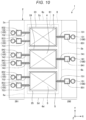
- FIG. 10 is a partially enlarged plan view illustrating an inertial sensor of a third embodiment.
- the third embodiment is the same as the first embodiment described above except that an inspection terminal 100 electrically coupled to the terminals 831 to 833 , 841 to 843 , and 851 to 853 is included.
- the third embodiment will be described with a focus on differences from the first and second embodiments, and description of similar matters will be omitted.
- FIG. 10 the same reference numerals are given to the same configurations as those in the first and second embodiments described above.
- the inertial sensor 1 includes an inspection terminal 100 provided on the exposed portions 291 and 292 of the substrate 2 and is electrically coupled to the terminals 831 to 833 , 841 to 843 , and 851 to 853 .
- the inspection terminal 100 includes an inspection terminal 131 that is disposed side by side with the terminal 831 and is electrically coupled to the terminal 831 , an inspection terminal 132 that is disposed side by side with the terminal 832 and is electrically coupled to the terminal 832 , an inspection terminal 133 that is disposed side by side with the terminal 833 and is electrically coupled to the terminal 833 , an inspection terminal 141 that is disposed side by side with the terminal 841 and is electrically coupled to the terminal 841 , an inspection terminal 142 that is disposed side by side with the terminal 842 and is electrically coupled to the terminal 842 , an inspection terminal 143 that is disposed side by side with the terminal 843 and is electrically coupled to the terminal 843 , an inspection terminal 151 that is disposed side by side with the terminal 851 and is electrically coupled to the terminal 851 , an inspection terminal 152 that is disposed side by side with the terminal 852 and is electrically coupled to the terminal 852 , and an inspection terminal 153 that is disposed side by side with the terminal 8
- the inertial sensor 1 can be inspected by pressing an inspection probe against the inspection terminals 131 , 132 , 133 , 141 , 142 , 143 , 151 , 152 , and 153 , and thus the terminals 831 , 832 , 833 , 841 , 842 , 843 , 851 , 852 , and 853 are not damaged during inspection. For that reason, the bonding wire and each terminal can be coupled well, and the inertial sensor 1 with high reliability is obtained.
- the inspection terminals 131 , 132 , 133 , 141 , 142 , 143 , 151 , 152 , and 153 have a shape in plan view different from that of the terminals 831 , 832 , 833 , 841 , 842 , 843 , 851 , 852 , and 853 , respectively.
- Each of the inspection terminals 131 , 132 , 133 , 141 , 142 , 143 , 151 , 152 , and 153 has a circular shape in plan view, and the shape in plan view is rotationally symmetric.
- the inspection terminals 131 , 132 , 133 , 141 , 142 , 143 , 151 , 152 , and 153 in plan view different from that of the terminals 831 , 832 , 833 , 841 , 842 , 843 , 851 , 852 , and 853 and setting the shape of the inspection terminals 131 , 132 , 133 , 141 , 142 , 143 , 151 , 152 , and 153 in plan view to be rotationally symmetric, the inspection terminals 131 , 132 , 133 , 141 , 142 , 143 , 151 , 152 , and 153 can be easily recognized by an image recognition technique when the inertial sensor 1 is inspected, for example.
- the shape of the inspection terminals 131 , 132 , 133 , 141 , 142 , 143 , 151 , 152 , and 153 is not particularly limited, and the shape of the inspection terminals 131 , 132 , 133 , 141 , 142 , 143 , 151 , 152 , and 153 may be the same shape as the terminal 831 , 832 , 833 , 841 , 842 , 843 , 851 , 852 , and 853 or may be a shape other than the rotationally symmetric shape.
- the inertial sensor 1 of the third embodiment includes a plurality of inspection terminals 131 , 132 , 133 , 141 , 142 , 143 , 151 , 152 , and 153 that are coupled to the plurality of terminals 831 , 832 , 833 , 841 , 842 , 843 , 851 , 852 , and 853 and have a shape in plan view different from that of the plurality of terminals 831 , 832 , 833 , 841 , 842 , 843 , 851 , 852 , and 853 .
- the inspection of the inertial sensor 1 can be performed using the inspection terminals 131 , 132 , 133 , 141 , 142 , 143 , 151 , 152 , and 153 , and thus the terminals 831 , 832 , 833 , 841 , 842 , 843 , 851 , 852 , and 853 will not be damaged during inspection. For that reason, the inertial sensor 1 with high reliability is obtained.
- the inspection terminals 131 , 132 , 133 , 141 , 142 , 143 , 151 , 152 , and 153 and the terminals 831 , 832 , 833 , 841 , 842 , 843 , 851 , 852 , and 853 can be easily identified.
- the shapes of the plurality of inspection terminals 131 , 132 , 133 , 141 , 142 , 143 , 151 , 152 , and 153 in plan view are rotationally symmetric.
- the inspection terminals 131 , 132 , 133 , 141 , 142 , 143 , 151 , 152 , and 153 can be easily recognized by an image recognition technique, and the inertial sensor 1 can be inspected more smoothly.
- the input terminals 831 , 841 , and 851 and the detection terminals 832 , 833 , 842 , 843 , 852 , and 853 are provided at opposite sides with the lid 6 interposed therebetween, but the inspection terminals 100 coupled to these input terminals and detection terminals are also disposed in the same manner.
- the same effect as that of the first embodiment described above can be exhibited not only during normal operation of the inertial sensor 1 but also during inspection using the inspection terminal 100 .
- FIG. 11 is a plan view illustrating an inertial sensor of the fourth embodiment.
- FIG. 12 is a plan view illustrating an example of a sensor element that measures an angular velocity around the X-axis.
- FIG. 13 is a plan view illustrating an example of a sensor element that measures an angular velocity around the Y-axis.
- FIG. 14 is a plan view illustrating an example of a sensor element that measures an angular velocity around the Z-axis.
- FIG. 15 is a graph illustrating a voltage applied to the sensor element.
- the sensor elements 300 , 400 , and 500 are illustrated in a simplified manner.
- the fourth embodiment is the same as the first embodiment described above except that sensor elements 300 , 400 , and 500 are used instead of the sensor elements 3 , 4 , and 5 .
- the fourth embodiment will be described with a focus on differences from the first to third embodiments described above, and description of similar matters will be omitted.
- FIGS. 11 to 15 the same reference numerals are given to the same configurations as those in the first to third embodiments described above.
- the inertial sensor 1 illustrated in FIG. 11 is an angular velocity sensor that can independently measure angular velocities around the X-, Y-, and Z-axes that are orthogonal to each other.
- Such an inertial sensor 1 includes the substrate 2 , three sensor elements 300 , 400 , and 500 disposed on the substrate 2 , and the lid 6 that accommodates the sensor elements 300 , 400 , and 500 and is bonded to the substrate 2 .
- the sensor element 300 (first inertial sensor element) measures an angular velocity ox around the X-axis
- the sensor element 400 measures the angular velocity coy around the Y-axis
- the sensor element 500 (third inertial sensor element) measures the angular velocity oz around the Z-axis.
- the accommodation space S formed by the substrate 2 and the lid 6 may be in a reduced pressure state, and particularly may be in a vacuum state.
- viscous resistance is reduced and the sensor elements 300 , 400 , and 500 can be vibrated effectively. For that reason, detection accuracy of the inertial sensor 1 is improved.
- a highly airtight accommodation space S can be formed by directly bonding the lid 6 to the substrate 2 .
- the substrate 2 has a groove that open to its upper surface, and a plurality of wirings 7310 , 7320 , 7330 , 7340 , 7350 , 7360 , 7370 , 7410 , 7420 , 7430 , 7440 , 7450 , 7460 , 7470 , 7510 , 7520 , 7530 , 7540 , 7550 , 7560 , and 7570 and terminals 8310 , 8320 , 8330 , 8340 , 8350 , 8360 , 8370 , 8410 , 8420 , 8430 , 8440 , 8450 , 8460 , 8470 , 8510 , 8520 , 8530 , 8540 , 8550 , 8560 , and 8570 are disposed in the groove.
- the wirings 7310 to 7370 , 7410 to 7470 , 7510 to 7570 are disposed inside and outside of the accommodation space S, and, among these wirings, each of the wirings 7310 to 7370 is electrically coupled to the sensor element 300 , each of the wirings 7410 to 7470 is electrically coupled to the sensor element 400 , and each of the wirings 7510 to 7570 is electrically coupled to the sensor element 500 .
- the terminals 8310 to 8370 , 8410 to 8470 , and 8510 to 8570 are positioned outside the lid 6 and are provided by being divided into the exposed portions 291 and 292 .
- the terminals 8310 to 8370 are electrically coupled to the wirings 7310 to 7370
- the terminals 8410 to 8470 are electrically coupled to the wirings 7410 to 7470
- the terminals 8510 to 8570 are electrically coupled to the wirings 7510 to 7570 .
- the sensor elements 300 , 400 , and 500 can be collectively formed by anodically bonding a silicon substrate doped with impurities such as phosphorus (P), boron (B), and arsenic (As) to the upper surface of the substrate 2 and patterning the silicon substrate by a Bosch process that is a deep groove etching technique.
- impurities such as phosphorus (P), boron (B), and arsenic (As)
- P phosphorus
- B boron
- As arsenic
- the method of forming the sensor elements 300 , 400 , 500 is not limited thereto.
- the sensor element 300 can measure the angular velocity ⁇ x around the X-axis.
- a sensor element 300 includes, for example, frame-like drive movable bodies 301 A and 301 B, drive springs 302 A and 302 B for supporting the drive movable bodies 301 A and 301 B so as to vibrate in the Y-axis direction, movable drive electrodes 303 A and 303 B coupled to the drive movable bodies 301 A and 301 B, first and second fixed drive electrodes 304 A and 305 A disposed with the movable drive electrode 303 A interposed therebetween, first and second fixed drive electrodes 304 B and 305 B disposed with the movable drive electrode 303 B interposed therebetween, detection movable bodies 306 A and 306 B disposed inside the drive movable bodies 301 A and 301 B, detection springs 307 A and 307 B coupling the detection movable bodies 306 A and 306 B and the drive movable bodies 301 A and 301 B
- the detection movable bodies 306 A and 306 B are electrically coupled to the wiring 7310
- the first fixed drive electrodes 304 A and 304 B are electrically coupled to the wiring 7320
- the second fixed drive electrodes 305 A and 305 B are electrically coupled to the wiring 7330
- the fixed detection electrode 312 A is electrically coupled to the wiring 7340
- the fixed detection electrode 312 B is electrically coupled to the wiring 7350
- the first fixed monitor electrodes 310 A and 310 B are electrically coupled to the wiring 7360
- the second fixed monitor electrodes 311 A and 311 B are electrically coupled to the wiring 7370 .
- a drive signal V 11 illustrated in FIG. 15 is applied to the detection movable bodies 306 A and 306 B via the terminal 8310 .
- a drive signal V 12 illustrated in FIG. 15 is applied to the first fixed drive electrodes 304 A and 304 B via the terminal 8320
- a drive signal V 13 illustrated in FIG. 15 is applied to the second fixed drive electrodes 305 A and 305 B via the terminal 8330 .
- the drive signal V 11 is, for example, 15 V
- the drive signal V 12 is, for example, a voltage having amplitude of ⁇ 0.2 V with respect to the analog ground AGND
- the drive signal V 13 is, for example, a voltage, whose phase is opposite to the drive signal V 12 , having amplitude of ⁇ 0.2 V with respect to the analog ground AGND.
- the fixed detection electrodes 312 A and 312 B are coupled to the charge amplifier through terminals 8340 and 8350 .
- the capacitance Cx 1 is formed between the detection movable body 306 A and the fixed detection electrode 312 A
- the capacitance Cx 2 is formed between the detection movable body 306 B and the fixed detection electrode 312 B.
- the detection movable bodies 306 A and 306 B are displaced in the Z-axis direction in opposite phases with each other by the Coriolis force, and accordingly the capacitances Cx 1 and Cx 2 change in opposite phases. For that reason, the amount of charge induced between the detection movable body 306 A and the fixed detection electrode 312 A and the amount of charge induced between the detection movable body 306 B and the fixed detection electrode 312 B also change based on the changes in the capacitances Cx 1 and Cx 2 .
- the difference is output as the voltage value of the charge amplifier. In this way, the angular velocity ⁇ x received by the sensor element 300 can be obtained.
- the sensor element 400 can measure the angular velocity coy around the Y-axis.
- a sensor element 400 is not particularly limited, but, for example, as illustrated in FIG. 13 , can be configured by rotating the sensor element 300 described above by 90 degrees around the Z-axis.
- such a sensor element 400 includes, for example, frame-like drive movable bodies 401 A and 401 B, drive springs 402 A and 402 B for supporting the drive movable bodies 401 A and 401 B so as to vibrate in the Y-axis direction, movable drive electrodes 403 A and 403 B coupled to the drive movable bodies 401 A and 401 B, first and second fixed drive electrodes 404 A and 405 A disposed with the movable drive electrode 403 A interposed therebetween, first and second fixed drive electrodes 404 B and 405 B disposed with the movable drive electrode 403 B interposed therebetween, detection movable bodies 406 A and 406 B disposed inside the drive movable bodies 401 A and 401 B, detection springs 407 A and 407 B coupling the detection movable bodies 406 A and 406 B and the drive movable bodies 401 A and 401 B, first movable monitor electrodes 408 A and 408 B and second mov
- the detection movable bodies 406 A and 406 B are electrically coupled to the wiring 7410
- the first fixed drive electrodes 404 A and 404 B are electrically coupled to the wiring 7420
- the second fixed drive electrodes 405 A and 405 B are electrically coupled to the wiring 7430
- the fixed detection electrode 412 A is electrically coupled to the wiring 7440
- the fixed detection electrode 412 B is electrically coupled to the wiring 7450
- the first fixed monitor electrodes 410 A and 410 B are coupled to the wiring 7460
- the second fixed monitor electrodes 411 A and 411 B are electrically coupled to the wiring 7470 .
- the drive signal V 11 illustrated in FIG. 15 is applied to the detection movable bodies 406 A and 406 B via the terminal 8410 .
- the drive signal V 12 illustrated in FIG. 15 is applied to the first fixed drive electrodes 404 A and 404 B via the terminal 8420
- the drive signal V 13 illustrated in FIG. 15 is applied to the second fixed drive electrodes 405 A and 405 B via the terminal 8430 .
- the drive signal V 11 is, for example, 15 V
- the drive signal V 12 is, for example, a voltage having amplitude of ⁇ 0.2 V with respect to the analog ground AGND
- the drive signal V 13 is, for example, a voltage, whose phase is opposite to the drive signal V 12 , having amplitude of ⁇ 0.2 V with respect to the analog ground AGND.
- the fixed detection electrodes 412 A and 412 B are coupled to the charge amplifier through terminals 8440 and 8450 .
- the capacitance Cy 1 is formed between the detection movable body 406 A and the fixed detection electrode 412 A
- the capacitance Cy 2 is formed between the detection movable body 406 B and the fixed detection electrode 412 B.
- the amount of charge induced between the detection movable body 406 A and the fixed detection electrode 412 A and the amount of charge induced between the detection movable body 406 B and the fixed detection electrode 412 B also change based on the changes in the capacitances Cy 1 and Cy 2 .
- the difference is output as the voltage value of the charge amplifier. In this way, the angular velocity coy received by the sensor element 400 can be obtained.
- the sensor element 500 can measure the angular velocity ⁇ z around the Z-axis.
- a sensor element 500 is not particularly limited, but, as illustrated in FIG. 14 , includes, for example, frame-like drive movable bodies 501 A and 501 B, drive springs 502 A and 502 B for supporting the drive movable bodies 501 A and 501 B so as to vibrate in the Y-axis direction, movable drive electrodes 503 A and 503 B coupled to the drive movable bodies 501 A and 501 B, first and second fixed drive electrodes 504 A and 505 A disposed with the movable drive electrode 503 A interposed therebetween, first and second fixed drive electrodes 504 B and 505 B disposed with the movable drive electrode 503 B interposed therebetween, detection movable bodies 506 A and 506 B disposed inside the drive movable bodies 501 A and 501 B, detection springs 507 A and 507 B coupling the detection movable bodies 506 A and 506 B and the drive movable
- the detection movable bodies 506 A and 506 B are electrically coupled to the wiring 7510
- the first fixed drive electrodes 504 A and 504 B are electrically coupled to the wiring 7520
- the second fixed drive electrodes 505 A and 505 B are electrically coupled to the wiring 7530
- the first fixed detection electrodes 513 A and 513 B are electrically coupled to the wiring 7540
- the second fixed detection electrodes 514 A and 514 B are electrically coupled to the wiring 7550
- the first fixed monitor electrodes 510 A and 510 B are electrically coupled to the wiring 7560
- the second fixed monitor electrodes 511 A and 511 B are electrically coupled to the wiring 7570 .
- the drive signal V 11 illustrated in FIG. 15 is applied to the detection movable bodies 506 A and 506 B via the terminal 8510 .
- the drive signal V 12 illustrated in FIG. 15 is applied to the first fixed drive electrodes 504 A and 504 B via a terminal 8520
- the drive signal V 13 illustrated in FIG. 15 is applied to the second fixed drive electrodes 505 A and 505 B via the terminal 8530 .
- the drive signal V 11 is, for example, 15 V
- the drive signal V 12 is, for example, a voltage having amplitude of ⁇ 0.2 V with respect to the analog ground AGND
- the drive signal V 13 is, for example, a voltage, whose phase is opposite to the drive signal V 12 , having amplitude of ⁇ 0.2 V with respect to the analog ground AGND.
- the first fixed detection electrodes 513 A and 513 B are coupled to the charge amplifier through the terminal 8540
- the second fixed detection electrodes 514 A and 514 B are coupled to the charge amplifier through the terminal 8550 .
- the capacitance Cz 1 is formed between the movable detection electrodes 512 A and 512 B and the first fixed detection electrodes 513 A and 513 B
- the capacitance Cz 2 is formed between the movable detection electrodes 512 A and 512 B and the second fixed detection electrodes 514 A and 514 B.
- the detection movable bodies 506 A and 506 B are displaced in the X-axis direction in opposite phases with each other by the Coriolis force, and accordingly the capacitances Cz 1 and Cz 2 change in opposite phases.
- the amount of charge induced between the movable detection electrodes 512 A and 512 B and the first fixed detection electrodes 513 A and 513 B, and the amount of charge induced between the movable detection electrodes 512 A and 512 B and the second fixed detection electrodes 514 A and 514 B also change based on the changes in the capacitances Cz 1 and Cz 2 .
- the difference is output as the voltage value of the charge amplifier. In this way, the angular velocity ⁇ z received by the sensor element 500 can be obtained.
- the sensor elements 300 , 400 , and 500 have been described as above.
- the configurations of the sensor elements 300 , 400 , and 500 are not particularly limited as long as the angular velocities ⁇ x, ⁇ y, and ⁇ z can be detected.
- Each of the terminals 8310 to 8370 is electrically coupled to the sensor element 300 .
- the terminals 8310 , 8320 , and 8330 are first drive signal terminals for inputting the drive signals V 11 to V 13 to the sensor element 300
- the terminals 8340 and 8350 are first detection signal terminals for detecting the detection signals detected by the sensor element 300 , that is, signals corresponding to the capacitances Cx 1 and Cx 2
- the terminals 8360 and 8370 are first pickup signal terminals for detecting the first and second pickup signals detected by the sensor element 300 .
- the terminals 8310 , 8320 , and 8330 are also referred to as “first drive signal terminals 8310 , 8320 , and 8330 ”, the terminals 8340 and 8350 are also referred to as “first detection signal terminals 8340 and 8350 ”, and the terminals 8360 and 8370 are also referred to as “first pickup signal terminals 8360 and 8370 ”.
- each of the terminals 8410 to 8470 is electrically coupled to the sensor element 400 .
- the terminals 8410 , 8420 , and 8430 are second drive signal terminals for inputting the drive signals V 11 to V 13 to the sensor element 400
- the terminals 8440 and 8450 are second detection signal terminals for detecting the detection signals detected by the sensor element 400 , that is, signals corresponding to the capacitances Cy 1 and Cy 2
- the terminals 8460 and 8470 are second pickup signal terminals for detecting the first and second pickup signals detected by the sensor element 400 .
- the terminals 8410 , 8420 , and 8430 are also referred to as “second drive signal terminals 8410 , 8420 , and 8430 ”, the terminals 8440 and 8450 are also referred to as “second detection signal terminals 8440 and 8450 ”, and the terminals 8460 and 8470 are also referred to as “second pickup signal terminals 8460 and 8470 ”.
- each of the terminals 8510 to 8570 is electrically coupled to the sensor element 500 .
- the terminals 8510 , 8520 , and 8530 are third drive signal terminals for inputting the drive signals V 11 to V 13 to the sensor element 500
- the terminals 8540 and 8550 are third detection signal terminals for detecting the detection signals detected by the sensor element 500 , that is, signals corresponding to the capacitances Cz 1 and Cz 2
- the terminals 8560 and 8570 are third pickup signal terminals for detecting the first and second pickup signals detected by the sensor element 500 .
- the terminals 8510 , 8520 , and 8530 are also referred to as “third drive signal terminals 8510 , 8520 , and 8530 ”, the terminals 8540 and 8550 are also referred to as “third detection signal terminals 8540 and 8550 ”, and the terminals 8560 and 8570 are also referred to as “third pickup signal terminals 8560 and 8570 ”.
- the terminals 8310 to 8370 , 8410 to 8470 , and 8510 to 8570 include the first, second, and third drive signal terminals 8310 to 8330 , 8410 to 8430 , and 8510 to 8530 that are input terminals for the drive signals V 11 , V 12 , and V 13 , the first, second, and third detection signal terminals 8340 , 8350 , 8440 , 8450 , 8540 , and 8550 that are detection terminals for the detection signals, and the first, second, and third pickup signal terminals 8360 , 8370 , 8460 , 8470 , 8560 , and 8570 that are detection terminals for the first and second pickup signals.
- the first, second, and third drive signal terminals 8310 to 8330 , 8410 to 8430 , and 8510 to 8530 are provided on the exposed portion 292
- the first, second, and third detection signal terminals 8340 , 8350 , 8440 , 8450 , 8540 , and 8550 are provided on the exposed portion 291
- the first, second, and third pickup signal terminals 8360 , 8370 , 8460 , 8470 , 8560 , and 8570 are provided on the exposed portion 292 .
- the first, second, and third drive signal terminals 8310 to 8330 , 8410 to 8430 , and 8510 to 8530 , the first, second, and third pickup signal terminals 8360 , 8370 , 8460 , 8470 , 8560 , and 8570 , and the first, second, and third detection signal terminals 8340 , 8350 , 8440 , 8450 , 8540 , and 8550 are provided at opposite sides with the lid 6 interposed therebetween in plan view from the Z-axis direction.
- the first, second, and third detection signal terminals 8340 , 8350 , 8440 , 8450 , 8540 , and 8550 can be disposed sufficiently apart from the first, second, and third drive signal terminals 8310 to 8330 , 8410 to 8430 , and 8510 to 8530 .
- the drive signals V 11 , V 12 , and V 13 input from the first, second, and third drive signal terminals 8310 to 8330 , 8410 to 8430 , and 8510 to 8530 to be mixed into the detection signals detected from the first, second, and third detection signal terminals 8340 , 8350 , 8440 , 8450 , 8540 , and 8550 as noise, and degradation of the S/N ratio of the detection signals can be suppressed. Since the detection signals are very weak signals with respect to the drive signals V 11 , V 12 , and V 13 , the effect described above is exceptional.
- first, second, and third detection signal terminals 8340 , 8350 , 8440 , 8450 , 8540 , and 8550 can be disposed sufficiently apart from the first, second, and third pickup signal terminals 8360 , 8370 , 8460 , 8470 , 8560 , and 8570 .
- first and second pickup signals detected from the first, second, and third pickup signal terminals 8360 , 8370 , 8460 , 8470 , 8560 , and 8570 it becomes difficult for the first and second pickup signals detected from the first, second, and third pickup signal terminals 8360 , 8370 , 8460 , 8470 , 8560 , and 8570 to be mixed into the detection signals detected from the first, second, and third detection signal terminals 8340 , 8350 , 8440 , 8450 , 8540 , and 8550 as noise, and degradation of the S/N ratio of the detection signals can be suppressed.
- the sensor element 300 as the first inertial sensor element is a gyro sensor element that measures an angular velocity, and includes the drive movable bodies 301 A and 301 B that vibrate with respect to the substrate 2 .
- the inertial sensor 1 includes the first pickup signal terminals 8360 and 8370 that are provided outside the lid 6 and are for pickup signals corresponding to vibrations of the drive movable bodies 301 A and 301 B detected by the sensor element 300 .
- the first pickup signal terminals 8360 and 8370 are positioned at the same side as the first drive signal terminals 8310 to 8330 with respect to the lid 6 , that is, on the plus side in the X-axis direction.
- the first detection signal terminals 8340 and 8350 can be disposed sufficiently apart from the first pickup signal terminals 8360 and 8370 . For that reason, it becomes difficult for the pickup signals detected from the first pickup signal terminals 8360 and 8370 to be mixed into the detection signals detected from the first detection signal terminals 8340 and 8350 as noise, and degradation of the S/N ratio of the detection signals can be suppressed.
- FIG. 16 is a plan view illustrating an inertial sensor of the fifth embodiment.
- FIG. 17 is a plan view illustrating an example of a sensor element.
- the sensor elements 300 , 400 , and 500 are illustrated in a simplified manner.
- the fifth embodiment is the same as the first and fourth embodiments described above, except that the sensor elements 300 , 400 , and 500 of the fourth embodiment described above are integrated.
- the fifth embodiment will be described with a focus on differences from the embodiments described above, and description of similar matters will be omitted.
- FIGS. 16 to 17 the same reference numerals are given to the same configurations as those of the embodiments described above.
- the movable drive electrodes 303 A and 303 B, the first and second fixed drive electrodes 304 A, 304 B, 305 A, and 305 B, the first and second movable monitor electrodes 308 A, 308 B, 309 A, and 309 B, and the first and second fixed monitor electrodes 310 A, 310 B, 311 A, and 311 B of the sensor element 300 also serve as corresponding portions of the sensor elements 400 and 500 .
- the movable drive electrodes 403 A and 403 B, the first and second fixed drive electrodes 404 A, 404 B, 405 A, and 405 B, the first and second movable monitor electrodes 408 A, 408 B, 409 A, and 409 B, and the first and second fixed monitor electrodes 410 A, 410 B, 411 A, and 411 B are omitted from the sensor element 400 , and the movable drive electrodes 503 A and 503 B, the first and second fixed drive electrodes 504 A, 504 B, 505 A, and 505 B, the first and second movable monitor electrodes 508 A, 508 B, 509 A, and 509 B, and the first and second fixed monitor electrodes 510 A, 510 B, 511 A, and 511 B are omitted from the sensor element 500 .
- the sensor element 300 includes the frame-like drive movable bodies 301 A and 301 B, drive springs 302 A and 302 B for supporting the drive movable bodies 301 A and 301 B so as to vibrate in the Y-axis direction, movable drive electrodes 303 A and 303 B coupled to the drive movable bodies 301 A and 301 B, first and second fixed drive electrodes 304 A and 305 A disposed with the movable drive electrode 303 A interposed therebetween, first and second fixed drive electrodes 304 B and 305 B disposed with the movable drive electrode 303 B interposed therebetween, detection movable bodies 306 A and 306 B provided inside the drive movable bodies 301 A and 301 B, detection springs 307 A and 307 B coupling the detection movable bodies 306 A and 306 B and the drive movable bodies 301 A and 301 B, first movable monitor electrode 308 A provided on the movable drive electrode 303 A, second movable monitor electrode
- the detection movable bodies 306 A and 306 B are electrically coupled to the wiring 7310
- the first fixed drive electrodes 304 A and 304 B are electrically coupled to the wiring 7320
- the second fixed drive electrodes 305 A and 305 B are electrically coupled to the wiring 7330
- the fixed detection electrode 312 A is electrically coupled to the wiring 7340
- the fixed detection electrode 312 B is electrically coupled to the wiring 7350
- the first fixed monitor electrode 310 A is electrically coupled to the wiring 7360
- the second fixed monitor electrode 311 B is electrically coupled to the wiring 7370 .
- the sensor element 400 includes the frame-like drive movable bodies 401 A and 401 B, drive springs 402 A and 402 B for supporting the drive movable bodies 401 A and 401 B so as to vibrate in the X-axis direction, detection movable bodies 406 A and 406 B disposed inside the drive movable bodies 401 A and 401 B, detection springs 407 A and 407 B coupling the detection movable bodies 406 A and 406 B and the drive movable bodies 401 A and 401 B, conversion units 413 A and 413 B that are provided between the movable drive electrodes 303 A and 303 B and the drive movable bodies 401 A and 401 B and convert vibrations in the Y-axis direction of the movable drive electrodes 303 A and 303 B into vibrations in the X-axis direction.
- the fixed detection electrodes 412 A and 412 B are disposed on the bottom surface of the concave portion 23 so as to face the drive movable bodies 401 A and 401
- the fixed detection electrode 412 A is electrically coupled to the wiring 7440
- the fixed detection electrode 412 B is electrically coupled to the wiring 7450 .
- the sensor element 500 includes the frame-like drive movable bodies 501 A and 501 B, drive springs 502 A and 502 B for supporting the drive movable bodies 501 A and 501 B so as to vibrate in the Y-axis direction, frame-like detection movable bodies 506 A and 506 B disposed inside the drive movable bodies 501 A and 501 B, detection springs 507 A and 507 B coupling the detection movable bodies 506 A and 506 B and the drive movable bodies 501 A and 501 B, movable detection electrodes 512 A and 512 B supported by the detection movable bodies 506 A and 506 B, first and second fixed detection electrodes 513 A and 514 A disposed with the movable detection electrode 512 A interposed therebetween, and first and second fixed detection electrodes 513 B and 514 B disposed with the movable detection electrode 512 B interposed therebetween.
- the first fixed detection electrodes 513 A and 513 B are electrically coupled to the wiring 7540
- the second fixed detection electrodes 514 A and 514 B are electrically coupled to the wiring 7550 .
- the wirings 7340 and 7350 can be disposed symmetrically with respect to the center line Lx that passes through the center O of the inertial sensor 1 and extends in the X-axis direction, and it becomes easy to design the lengths of the wirings 7340 and 7350 equal to each other.
- FIG. 18 is a plan view illustrating an inertial sensor unit of the sixth embodiment.
- FIG. 19 is a cross-sectional view of the inertial sensor unit illustrated in FIG. 18 .
- An inertial sensor unit 1000 illustrated in FIGS. 18 and 19 includes a package 1010 , an IC chip 1040 and an inertial sensor 1 that are accommodated in the package 1010 .
- the IC chip 1040 for example, a drive control circuit that controls driving of the inertial sensor 1 and a detection circuit that measures accelerations Ax, Ay, and Az based on detection signals from the inertial sensor 1 are included.
- the configuration of the first embodiment described above is used as the configuration of the inertial sensor 1 , but the configuration of the inertial sensor 1 is not particularly limited thereto and may be any of those configurations of other embodiments.
- the package 1010 includes a base substrate 1020 having a concave portion 1021 which opens to the upper surface, and a lid 1030 bonded to the upper surface of the base substrate 1020 so as to close the opening of the concave portion 1021 .
- the concave portion 1021 includes a first concave portion 1022 which opens to the upper surface of the base substrate 1020 and a second concave portion 1023 which opens to the bottom surface of the first concave portion 1022 .
- An IC chip 1040 is mounted on the bottom surface of the second concave portion 1023 and the inertial sensor 1 is mounted on the IC chip 1040 .
- the terminals 831 to 833 , 841 to 843 , and 851 to 853 of the inertial sensor 1 are electrically coupled to corresponding terminals of IC chip 1040 through bonding wires BW 1 . Since the terminals 831 to 833 , 841 to 843 , and 851 to 853 of the inertial sensor 1 are disposed as described above, it becomes difficult for noise to be mixed into the detection signal detected from the inertial sensor 1 .
- a plurality of internal terminals 1050 that are electrically coupled to the IC chip 1040 through bonding wires BW 2 are disposed on the bottom surface of the first concave portion 1022 .
- a plurality of external terminals 1060 that are electrically coupled to a plurality of internal terminals 1050 through internal wirings (not illustrated) disposed in the base substrate 1020 are disposed on the lower surface of the base substrate 1020 .
- Such an inertial sensor unit 1000 includes the inertial sensor 1 . For that reason, the effects of the inertial sensor 1 described above can be obtained and high reliability can be exhibited.
- FIG. 20 is a plan view illustrating a smartphone of a seventh embodiment.
- the inertial sensor 1 and a control circuit 1210 that performs control based on detection signals detected from the inertial sensor 1 are incorporated.
- Detection data detected by the inertial sensor 1 is transmitted to the control circuit 1210 , and the control circuit 1210 can recognize the attitude and behavior of the smartphone 1200 from the received detection data, change a display image displayed on a display unit 1208 , generate an alarm sound or sound effect, or drive the vibration motor to vibrate the main body.
- the smartphone 1200 as such an electronic apparatus includes the inertial sensor 1 and the control circuit 1210 that performs control based on a detection signal output from the inertial sensor 1 . For that reason, the effect of the inertial sensor 1 described above can be obtained and high reliability can be exhibited.
- the electronic apparatus incorporating the inertial sensor 1 is not particularly limited, and includes, for example, a personal computer, a digital still camera, a tablet terminal, a timepiece, a smartwatch, an ink jet printer, a laptop personal computer, a TV, a wearable terminals such as HMD (head mounted display), a video camera, a video tape recorder, a car navigation device, a pager, an electronic datebook, an electronic dictionary, a calculator, an electronic game machine, a word processor, a work station, a videophone, a security TV monitor, electronic binoculars, a POS terminal, medical equipment, a fish finder, various measuring instruments, mobile terminal base station equipment, various instruments of vehicles, aircraft, and ships, a flight simulator, a network server, and the like, in addition to the smartphone 1200 .
- HMD head mounted display
- video camera a video tape recorder
- car navigation device a pager
- an electronic datebook an electronic dictionary
- a calculator an electronic game machine
- FIG. 21 is an exploded perspective view illustrating an inertia measurement device according to an eighth embodiment.
- FIG. 22 is a perspective view of a substrate included in the inertia measurement device illustrated in FIG. 21 .
- An inertia measurement device 2000 (IMU: Inertial measurement Unit) illustrated in FIG. 21 is an inertia measurement device that detects the attitude and behavior of amounted device such as an automobile or a robot.
- the inertia measurement device 2000 functions as a six-axis motion sensor including three-axis acceleration sensors and three-axis angular velocity sensors.
- the inertia measurement device 2000 is a rectangular parallelepiped having a substantially square planar shape. Screw holes 2110 as fixed portions are formed in the vicinity of two vertices positioned in the diagonal direction of the square. Through two screws in the two screw holes 2110 , the inertia measurement device 2000 can be fixed to the mounted surface of the mounted object such as an automobile. The size of the inertia measurement device 2000 can be reduced such that the device can be mounted on a smartphone or a digital still camera, for example, by selection of parts or design change.
- the inertia measurement device 2000 has a configuration in which an outer case 2100 , a bonding member 2200 , and a sensor module 2300 are included and the sensor module 2300 is inserted in the outer case 2100 with the bonding member 2200 interposed therebetween.
- the outer shape of the outer case 2100 is a rectangular parallelepiped having a substantially square planar shape, and screw holes 2110 are formed in the vicinity of two vertices positioned in the diagonal direction of the square.
- the outer case 2100 has a box shape and the sensor module 2300 is accommodated therein.
- the sensor module 2300 includes an inner case 2310 and a substrate 2320 .
- the inner case 2310 is a member for supporting the substrate 2320 , and has a shape that fits inside the outer case 2100 .
- a concave portion 2311 for suppressing contact with the substrate 2320 and an opening 2312 for exposing a connector 2330 described later are formed in the inner case 2310 .
- Such an inner case 2310 is bonded to the outer case 2100 through the bonding member 2200 .
- the substrate 2320 is bonded to the lower surface of the inner case 2310 through an adhesive.
- a connector 2330 an angular velocity sensor 2340 z for measuring the angular velocity around the Z-axis, an acceleration sensor 2350 for measuring acceleration in each axis direction of the X-axis, the Y-axis, and the Z-axis and the like are mounted on the upper surface of the substrate 2320 .
- An angular velocity sensor 2340 x for measuring the angular velocity around the X-axis and an angular velocity sensor 2340 y for measuring the angular velocity around the Y-axis are mounted on the side surface of the substrate 2320 .
- the inertial sensor of the embodiments can be used.
- a control IC 2360 is mounted on the lower surface of the substrate 2320 .
- the control IC 2360 is a micro controller unit (MCU) and controls each unit of the inertia measurement device 2000 .
- MCU micro controller unit
- programs defining the order and contents for measuring the acceleration and angular velocity, programs for digitizing detected data and incorporating the detected data into packet data, accompanying data, and the like are stored.
- a plurality of electronic components are mounted on the substrate 2320 .
- FIG. 23 is a block diagram illustrating the entire system of a vehicle positioning device according to a ninth embodiment.
- FIG. 24 is a diagram illustrating the operation of the vehicle positioning device illustrated in FIG. 23 .
- a vehicle positioning device 3000 illustrated in FIG. 23 is a device which is used by being mounted on a vehicle and performs positioning of the vehicle.
- the vehicle is not particularly limited, and may be any of a bicycle, an automobile, a motorcycle, a train, an airplane, a ship, and the like, but in the seventh embodiment, description will be made on a four-wheeled automobile as the vehicle.
- the vehicle positioning device 3000 includes an inertia measurement device 3100 (IMU), a computation processing unit 3200 , a GPS reception unit 3300 , a receiving antenna 3400 , a position information acquisition unit 3500 , a position synthesis unit 3600 , a processing unit 3700 , a communication unit 3800 , and a display 3900 .
- IMU inertia measurement device
- the inertia measurement device 3100 for example, the inertia measurement device 2000 described above can be used.
- the inertia measurement device 3100 includes a tri-axis acceleration sensor 3110 and a tri-axis angular velocity sensor 3120 .
- the computation processing unit 3200 receives acceleration data from the acceleration sensor 3110 and angular velocity data from the angular velocity sensor 3120 , performs inertial navigation computation processing on these data, and outputs inertial navigation positioning data including acceleration and attitude of the vehicle.
- the GPS reception unit 3300 receives a signal from the GPS satellite through the receiving antenna 3400 . Further, the position information acquisition unit 3500 outputs GPS positioning data representing the position (latitude, longitude, altitude), speed, direction of the vehicle positioning device 3000 based on the signal received by the GPS reception unit 3300 .
- the GPS positioning data also includes status data indicating a reception state, a reception time, and the like.
- the position synthesis unit 3600 calculates the position of the vehicle, more specifically, the position on the ground where the vehicle is traveling. For example, even if the position of the vehicle included in the GPS positioning data is the same, as illustrated in FIG. 24 , if the attitude of the vehicle is different due to the influence of inclination ⁇ of the ground or the like, the vehicle is traveling at different positions on the ground. For that reason, it is impossible to calculate an accurate position of the vehicle with only GPS positioning data. Therefore, the position synthesis unit 3600 calculates the position on the ground where the vehicle is traveling, using inertial navigation positioning data.
- the position data output from the position synthesis unit 3600 is subjected to predetermined processing by the processing unit 3700 and displayed on the display 3900 as a positioning result. Further, the position data may be transmitted to the external apparatus by the communication unit 3800 .
- FIG. 25 is a perspective view illustrating a vehicle according to a tenth embodiment of the disclosure.
- An automobile 1500 as the vehicle illustrated in FIG. 25 includes at least one system 1510 of an engine system, a brake system, and a keyless entry system.
- the inertial sensor 1 is incorporated in the automobile 1500 , and the attitude of the vehicle body can be measured by the inertial sensor 1 .
- the detection signal of the inertial sensor 1 is supplied to the control device 1502 , and the control device 1502 can control the system 1510 based on the signal.
- the automobile 1500 as the vehicle includes the inertial sensor 1 and the control device 1502 that performs control based on the detection signal output from the inertial sensor 1 . For that reason, the effect of the inertial sensor 1 described above can be obtained and high reliability can be exhibited.
- the inertial sensor 1 can also be widely applied to a car navigation system, a car air conditioner, an anti-lock braking system (ABS), an air bag, a tire pressure monitoring system (TPMS), an engine controller, and an electronic control unit (ECU) such as a battery monitor of a hybrid car or an electric automobile.
- the vehicle is not limited to the automobile 1500 , but can also be applied to an airplane, a rocket, a satellite, a ship, an automated guided vehicle (AGV), a biped walking robot, an unmanned airplane such as a drone, and the like.
- the inertial sensor according to the present disclosure has been described based on the embodiments, the disclosure is not limited thereto.
- the configuration of each unit can be replaced with any configuration having the same function.
Landscapes
- Physics & Mathematics (AREA)
- General Physics & Mathematics (AREA)
- Engineering & Computer Science (AREA)
- Radar, Positioning & Navigation (AREA)
- Remote Sensing (AREA)
- Microelectronics & Electronic Packaging (AREA)
- Electromagnetism (AREA)
- Computer Hardware Design (AREA)
- Pressure Sensors (AREA)
- Gyroscopes (AREA)
Abstract
Description
Claims (12)
Applications Claiming Priority (2)
| Application Number | Priority Date | Filing Date | Title |
|---|---|---|---|
| JP2019036744A JP2020139879A (en) | 2019-02-28 | 2019-02-28 | Inertia sensors, electronics and moving objects |
| JP2019-036744 | 2019-02-28 |
Publications (2)
| Publication Number | Publication Date |
|---|---|
| US20200278377A1 US20200278377A1 (en) | 2020-09-03 |
| US11714101B2 true US11714101B2 (en) | 2023-08-01 |
Family
ID=72236214
Family Applications (1)
| Application Number | Title | Priority Date | Filing Date |
|---|---|---|---|
| US16/802,137 Active 2040-12-30 US11714101B2 (en) | 2019-02-28 | 2020-02-26 | Inertial sensor, electronic apparatus, and vehicle |
Country Status (3)
| Country | Link |
|---|---|
| US (1) | US11714101B2 (en) |
| JP (1) | JP2020139879A (en) |
| CN (1) | CN111623760B (en) |
Families Citing this family (4)
| Publication number | Priority date | Publication date | Assignee | Title |
|---|---|---|---|---|
| JP6870635B2 (en) * | 2018-03-08 | 2021-05-12 | セイコーエプソン株式会社 | Inertial measurement units, mobiles, portable electronic devices, and electronic devices |
| JP2023092734A (en) * | 2021-12-22 | 2023-07-04 | セイコーエプソン株式会社 | Inertial measurement unit |
| JP2024101653A (en) * | 2023-01-18 | 2024-07-30 | セイコーエプソン株式会社 | Inertial sensors and inertial measurement units |
| DE102024202829A1 (en) * | 2024-03-25 | 2025-09-25 | Robert Bosch Gesellschaft mit beschränkter Haftung | Environmental sensor and method for operating an environmental sensor |
Citations (15)
| Publication number | Priority date | Publication date | Assignee | Title |
|---|---|---|---|---|
| WO1995021383A1 (en) * | 1994-02-04 | 1995-08-10 | The Charles Stark Draper Laboratory, Inc. | Method of making a micromechanical silicon-on-glass tuning fork gyroscope |
| JPH11211482A (en) | 1998-01-28 | 1999-08-06 | Aisin Seiki Co Ltd | Electrode structure of surface micromachine |
| US20010008089A1 (en) * | 2000-01-19 | 2001-07-19 | Alps Electric Co., Ltd. | Capacitive micro sensor, gyroscope, and input device |
| JP2001330442A (en) * | 2000-05-22 | 2001-11-30 | Toyota Motor Corp | Sensor element and sensor device |
| US20070031638A1 (en) * | 2005-08-08 | 2007-02-08 | Mitsubishi Denki Kabushiki Kaisha | Thin film structure and manufacturing method therefor |
| US20090183568A1 (en) * | 2008-01-21 | 2009-07-23 | Hitachi, Ltd. | Inertial sensor |
| WO2010103093A1 (en) * | 2009-03-11 | 2010-09-16 | Continental Teves Ag & Co. Ohg | Double-axial rotation rate sensor |
| US20150268266A1 (en) * | 2014-03-18 | 2015-09-24 | Seiko Epson Corporation | Electronic device, electronic apparatus, and moving object |
| JP2015177153A (en) | 2014-03-18 | 2015-10-05 | セイコーエプソン株式会社 | Electronic device, electronic module, electronic apparatus and movable body |
| JP2015206648A (en) | 2014-04-18 | 2015-11-19 | セイコーエプソン株式会社 | Electronic devices, electronic devices, and moving objects |
| JP2016133472A (en) * | 2015-01-22 | 2016-07-25 | セイコーエプソン株式会社 | Sensor devices, electronic devices, and moving objects |
| CN107063225A (en) * | 2015-11-04 | 2017-08-18 | 精工爱普生株式会社 | Electronic installation, the manufacture method of electronic installation, electronic equipment and moving body |
| JP2017173074A (en) | 2016-03-23 | 2017-09-28 | セイコーエプソン株式会社 | Sensor device, electronic apparatus, and movable body |
| US9823071B2 (en) | 2013-11-25 | 2017-11-21 | Seiko Epson Corporation | Package, electronic component mounted package, physical quantity sensor, electronic device, and moving object |
| JP2018169406A (en) | 2018-06-21 | 2018-11-01 | セイコーエプソン株式会社 | Electronic component mounting packages, physical quantity sensors, electronic devices and mobile objects |
Family Cites Families (4)
| Publication number | Priority date | Publication date | Assignee | Title |
|---|---|---|---|---|
| US8646332B2 (en) * | 2007-09-03 | 2014-02-11 | Panasonic Corporation | Inertia force sensor |
| JP4508230B2 (en) * | 2007-11-21 | 2010-07-21 | ソニー株式会社 | Inertial sensor and its detection device |
| CN202150775U (en) * | 2011-07-20 | 2012-02-22 | 佛山市威灵洗涤电机制造有限公司 | Installing structure of rotary motor electrical carbon fixing rack |
| CN206074798U (en) * | 2016-01-29 | 2017-04-05 | 中国矿业大学(北京) | The monitoring positioning and personnel's help system of the high disaster tolerance degree in down-hole |
-
2019
- 2019-02-28 JP JP2019036744A patent/JP2020139879A/en active Pending
-
2020
- 2020-02-26 US US16/802,137 patent/US11714101B2/en active Active
- 2020-02-27 CN CN202010125887.2A patent/CN111623760B/en active Active
Patent Citations (17)
| Publication number | Priority date | Publication date | Assignee | Title |
|---|---|---|---|---|
| WO1995021383A1 (en) * | 1994-02-04 | 1995-08-10 | The Charles Stark Draper Laboratory, Inc. | Method of making a micromechanical silicon-on-glass tuning fork gyroscope |
| JPH11211482A (en) | 1998-01-28 | 1999-08-06 | Aisin Seiki Co Ltd | Electrode structure of surface micromachine |
| US20010008089A1 (en) * | 2000-01-19 | 2001-07-19 | Alps Electric Co., Ltd. | Capacitive micro sensor, gyroscope, and input device |
| JP2001330442A (en) * | 2000-05-22 | 2001-11-30 | Toyota Motor Corp | Sensor element and sensor device |
| US20070031638A1 (en) * | 2005-08-08 | 2007-02-08 | Mitsubishi Denki Kabushiki Kaisha | Thin film structure and manufacturing method therefor |
| US20090183568A1 (en) * | 2008-01-21 | 2009-07-23 | Hitachi, Ltd. | Inertial sensor |
| WO2010103093A1 (en) * | 2009-03-11 | 2010-09-16 | Continental Teves Ag & Co. Ohg | Double-axial rotation rate sensor |
| US9823071B2 (en) | 2013-11-25 | 2017-11-21 | Seiko Epson Corporation | Package, electronic component mounted package, physical quantity sensor, electronic device, and moving object |
| JP2015177153A (en) | 2014-03-18 | 2015-10-05 | セイコーエプソン株式会社 | Electronic device, electronic module, electronic apparatus and movable body |
| US9321627B2 (en) | 2014-03-18 | 2016-04-26 | Seiko Epson Corporation | Electronic device, electronic module, electronic apparatus, and moving object |
| US20150268266A1 (en) * | 2014-03-18 | 2015-09-24 | Seiko Epson Corporation | Electronic device, electronic apparatus, and moving object |
| JP2015206648A (en) | 2014-04-18 | 2015-11-19 | セイコーエプソン株式会社 | Electronic devices, electronic devices, and moving objects |
| US9764940B2 (en) | 2014-04-18 | 2017-09-19 | Seiko Epson Corporation | Electronic device, electronic apparatus, and moving object |
| JP2016133472A (en) * | 2015-01-22 | 2016-07-25 | セイコーエプソン株式会社 | Sensor devices, electronic devices, and moving objects |
| CN107063225A (en) * | 2015-11-04 | 2017-08-18 | 精工爱普生株式会社 | Electronic installation, the manufacture method of electronic installation, electronic equipment and moving body |
| JP2017173074A (en) | 2016-03-23 | 2017-09-28 | セイコーエプソン株式会社 | Sensor device, electronic apparatus, and movable body |
| JP2018169406A (en) | 2018-06-21 | 2018-11-01 | セイコーエプソン株式会社 | Electronic component mounting packages, physical quantity sensors, electronic devices and mobile objects |
Also Published As
| Publication number | Publication date |
|---|---|
| CN111623760A (en) | 2020-09-04 |
| US20200278377A1 (en) | 2020-09-03 |
| CN111623760B (en) | 2023-09-29 |
| JP2020139879A (en) | 2020-09-03 |
Similar Documents
| Publication | Publication Date | Title |
|---|---|---|
| US11022625B2 (en) | Physical quantity sensor having a movable portion including a frame surrounding a fixed portion fixed to a substrate | |
| US11714101B2 (en) | Inertial sensor, electronic apparatus, and vehicle | |
| US11662360B2 (en) | Physical quantity sensor having a movable body formed with through-holes to reduce a difference between the inside-hole damping and the squeeze film damping | |
| US10900985B2 (en) | Physical quantity sensor, inertia measurement device, vehicle positioning device, electronic apparatus, and vehicle | |
| US11320451B2 (en) | Acceleration sensor, electronic device, and vehicle | |
| US11282808B2 (en) | Inertial sensor, electronic instrument, vehicle, and method for manufacturing inertial sensor | |
| US11204367B2 (en) | Physical quantity sensor, physical quantity sensor device, complex sensor device, inertial measurement unit, and vehicle | |
| US20200241032A1 (en) | Inertial sensor, electronic device, and vehicle | |
| US11674974B2 (en) | Inertial sensor, electronic device, and vehicle | |
| US11454645B2 (en) | Inertial sensor, electronic instrument, and vehicle | |
| US11084712B2 (en) | Physical quantity sensor with spring having protective beam | |
| EP3726226B1 (en) | Physical quantity sensor, electronic apparatus and vehicle comprising such a physical quantity sensor | |
| US11385255B2 (en) | Inertial sensor, electronic device, and vehicle | |
| US20200278376A1 (en) | Inertial sensor, electronic apparatus, and vehicle | |
| US11561101B2 (en) | Physical quantity sensor, inertia measurement device, vehicle positioning device, electronic apparatus, and vehicle | |
| US20200249022A1 (en) | Inertial sensor, electronic device, and vehicle | |
| US11231438B2 (en) | Inertial sensor, electronic device, and vehicle | |
| US11391753B2 (en) | Inertial sensor, electronic instrument, and vehicle | |
| JP2021032802A (en) | Inertia sensor, manufacturing method of inertia sensor, electronic device and mobile body |
Legal Events
| Date | Code | Title | Description |
|---|---|---|---|
| AS | Assignment |
Owner name: SEIKO EPSON CORPORATION, JAPAN Free format text: ASSIGNMENT OF ASSIGNORS INTEREST;ASSIGNOR:TAKIZAWA, TERUO;REEL/FRAME:051940/0502 Effective date: 20191219 |
|
| FEPP | Fee payment procedure |
Free format text: ENTITY STATUS SET TO UNDISCOUNTED (ORIGINAL EVENT CODE: BIG.); ENTITY STATUS OF PATENT OWNER: LARGE ENTITY |
|
| STPP | Information on status: patent application and granting procedure in general |
Free format text: DOCKETED NEW CASE - READY FOR EXAMINATION |
|
| STPP | Information on status: patent application and granting procedure in general |
Free format text: NON FINAL ACTION MAILED |
|
| STPP | Information on status: patent application and granting procedure in general |
Free format text: RESPONSE TO NON-FINAL OFFICE ACTION ENTERED AND FORWARDED TO EXAMINER |
|
| STPP | Information on status: patent application and granting procedure in general |
Free format text: NON FINAL ACTION MAILED |
|
| STPP | Information on status: patent application and granting procedure in general |
Free format text: NON FINAL ACTION MAILED |
|
| STPP | Information on status: patent application and granting procedure in general |
Free format text: RESPONSE TO NON-FINAL OFFICE ACTION ENTERED AND FORWARDED TO EXAMINER |
|
| STPP | Information on status: patent application and granting procedure in general |
Free format text: FINAL REJECTION MAILED |
|
| STPP | Information on status: patent application and granting procedure in general |
Free format text: PUBLICATIONS -- ISSUE FEE PAYMENT VERIFIED |
|
| STCF | Information on status: patent grant |
Free format text: PATENTED CASE |