US11680163B2 - Resin composition for optical waveguide cores, and dry film, optical waveguide core and photoelectric composite wiring board, each of which uses same - Google Patents
Resin composition for optical waveguide cores, and dry film, optical waveguide core and photoelectric composite wiring board, each of which uses same Download PDFInfo
- Publication number
- US11680163B2 US11680163B2 US16/755,284 US201816755284A US11680163B2 US 11680163 B2 US11680163 B2 US 11680163B2 US 201816755284 A US201816755284 A US 201816755284A US 11680163 B2 US11680163 B2 US 11680163B2
- Authority
- US
- United States
- Prior art keywords
- refractive index
- optical waveguide
- resin composition
- epoxy resin
- core
- Prior art date
- Legal status (The legal status is an assumption and is not a legal conclusion. Google has not performed a legal analysis and makes no representation as to the accuracy of the status listed.)
- Active, expires
Links
Images


Classifications
-
- C—CHEMISTRY; METALLURGY
- C08—ORGANIC MACROMOLECULAR COMPOUNDS; THEIR PREPARATION OR CHEMICAL WORKING-UP; COMPOSITIONS BASED THEREON
- C08L—COMPOSITIONS OF MACROMOLECULAR COMPOUNDS
- C08L63/00—Compositions of epoxy resins; Compositions of derivatives of epoxy resins
-
- C—CHEMISTRY; METALLURGY
- C08—ORGANIC MACROMOLECULAR COMPOUNDS; THEIR PREPARATION OR CHEMICAL WORKING-UP; COMPOSITIONS BASED THEREON
- C08G—MACROMOLECULAR COMPOUNDS OBTAINED OTHERWISE THAN BY REACTIONS ONLY INVOLVING UNSATURATED CARBON-TO-CARBON BONDS
- C08G59/00—Polycondensates containing more than one epoxy group per molecule; Macromolecules obtained by polymerising compounds containing more than one epoxy group per molecule using curing agents or catalysts which react with the epoxy groups
- C08G59/18—Macromolecules obtained by polymerising compounds containing more than one epoxy group per molecule using curing agents or catalysts which react with the epoxy groups ; e.g. general methods of curing
- C08G59/20—Macromolecules obtained by polymerising compounds containing more than one epoxy group per molecule using curing agents or catalysts which react with the epoxy groups ; e.g. general methods of curing characterised by the epoxy compounds used
- C08G59/32—Epoxy compounds containing three or more epoxy groups
- C08G59/38—Epoxy compounds containing three or more epoxy groups together with di-epoxy compounds
-
- C—CHEMISTRY; METALLURGY
- C09—DYES; PAINTS; POLISHES; NATURAL RESINS; ADHESIVES; COMPOSITIONS NOT OTHERWISE PROVIDED FOR; APPLICATIONS OF MATERIALS NOT OTHERWISE PROVIDED FOR
- C09D—COATING COMPOSITIONS, e.g. PAINTS, VARNISHES OR LACQUERS; FILLING PASTES; CHEMICAL PAINT OR INK REMOVERS; INKS; CORRECTING FLUIDS; WOODSTAINS; PASTES OR SOLIDS FOR COLOURING OR PRINTING; USE OF MATERIALS THEREFOR
- C09D163/00—Coating compositions based on epoxy resins; Coating compositions based on derivatives of epoxy resins
-
- G—PHYSICS
- G02—OPTICS
- G02B—OPTICAL ELEMENTS, SYSTEMS OR APPARATUS
- G02B1/00—Optical elements characterised by the material of which they are made; Optical coatings for optical elements
- G02B1/04—Optical elements characterised by the material of which they are made; Optical coatings for optical elements made of organic materials, e.g. plastics
- G02B1/045—Light guides
- G02B1/046—Light guides characterised by the core material
-
- G—PHYSICS
- G02—OPTICS
- G02B—OPTICAL ELEMENTS, SYSTEMS OR APPARATUS
- G02B1/00—Optical elements characterised by the material of which they are made; Optical coatings for optical elements
- G02B1/04—Optical elements characterised by the material of which they are made; Optical coatings for optical elements made of organic materials, e.g. plastics
- G02B1/045—Light guides
- G02B1/048—Light guides characterised by the cladding material
-
- G—PHYSICS
- G02—OPTICS
- G02B—OPTICAL ELEMENTS, SYSTEMS OR APPARATUS
- G02B6/00—Light guides; Structural details of arrangements comprising light guides and other optical elements, e.g. couplings
- G02B6/10—Light guides; Structural details of arrangements comprising light guides and other optical elements, e.g. couplings of the optical waveguide type
- G02B6/12—Light guides; Structural details of arrangements comprising light guides and other optical elements, e.g. couplings of the optical waveguide type of the integrated circuit kind
- G02B6/122—Basic optical elements, e.g. light-guiding paths
- G02B6/1221—Basic optical elements, e.g. light-guiding paths made from organic materials
-
- H—ELECTRICITY
- H05—ELECTRIC TECHNIQUES NOT OTHERWISE PROVIDED FOR
- H05K—PRINTED CIRCUITS; CASINGS OR CONSTRUCTIONAL DETAILS OF ELECTRIC APPARATUS; MANUFACTURE OF ASSEMBLAGES OF ELECTRICAL COMPONENTS
- H05K1/00—Printed circuits
- H05K1/02—Details
-
- C—CHEMISTRY; METALLURGY
- C08—ORGANIC MACROMOLECULAR COMPOUNDS; THEIR PREPARATION OR CHEMICAL WORKING-UP; COMPOSITIONS BASED THEREON
- C08L—COMPOSITIONS OF MACROMOLECULAR COMPOUNDS
- C08L2203/00—Applications
- C08L2203/20—Applications use in electrical or conductive gadgets
-
- C—CHEMISTRY; METALLURGY
- C08—ORGANIC MACROMOLECULAR COMPOUNDS; THEIR PREPARATION OR CHEMICAL WORKING-UP; COMPOSITIONS BASED THEREON
- C08L—COMPOSITIONS OF MACROMOLECULAR COMPOUNDS
- C08L2205/00—Polymer mixtures characterised by other features
- C08L2205/02—Polymer mixtures characterised by other features containing two or more polymers of the same C08L -group
- C08L2205/025—Polymer mixtures characterised by other features containing two or more polymers of the same C08L -group containing two or more polymers of the same hierarchy C08L, and differing only in parameters such as density, comonomer content, molecular weight, structure
-
- G—PHYSICS
- G02—OPTICS
- G02B—OPTICAL ELEMENTS, SYSTEMS OR APPARATUS
- G02B6/00—Light guides; Structural details of arrangements comprising light guides and other optical elements, e.g. couplings
- G02B6/10—Light guides; Structural details of arrangements comprising light guides and other optical elements, e.g. couplings of the optical waveguide type
- G02B6/12—Light guides; Structural details of arrangements comprising light guides and other optical elements, e.g. couplings of the optical waveguide type of the integrated circuit kind
- G02B6/13—Integrated optical circuits characterised by the manufacturing method
- G02B6/138—Integrated optical circuits characterised by the manufacturing method by using polymerisation
Definitions
- the present invention relates to a resin composition for optical waveguide cores. Furthermore, the present invention relates to a dry film, an optical waveguide core and a photoelectric composite wiring board, each of which uses such a resin composition.
- an optical fiber has been the mainstream as a transmission medium in the fields of FTTH (Fiber to the Home) and long distance and middle distance communication in the automotive equipment field. These days, high speed transmission using light is becoming necessary even for short distance within 1 m.
- an optical waveguide type light wiring board by which high density wiring (narrow pitches, branching, crossing, multi layering, etc.), surface mounting ability, integration with electric boards, and bending with small diameters can be achieved, these characteristics being unable to be achieved by an optical fiber, is suitable.
- a method of manufacturing an optical waveguide has been known ((1) a step of forming a cladding layer, a core layer, etc. by using a resin material with high transparency, (2) a step of performing exposure by irradiation with ultraviolet rays (UV) or the like, (3) a step of performing development, and (4) a step of curing the resin). It is reported that, as a material for such an optical waveguide, a resin composition containing liquid epoxy resin and solid epoxy resin is used as a photocurable resin in order to suppress stickiness and to improve productivity and processability (for example, Patent Literature 1).
- the liquid epoxy resin which is a low molecular component, is likely to move from an unexposed portion to an exposed portion (a core portion) due to a diffusion phenomenon.
- a portion having a lower refractive index than the interior of the core occurs on a side surface of the core, and after development the dark portion forms a part where light that is originally expected to pass through the interior of the core cannot pass.
- the width of the core through which light actually runs is made nonuniform, and the unclear width of the core causes problems such as the accuracy of alignment during mounting being reduced.
- an object of the present invention is to provide a resin composition for optical waveguide cores, the resin composition improving the issue mentioned above, i.e., narrowing the distribution of refractive indices of epoxy resins contained in the resin composition that forms a core, and thereby making it possible to suppress the formation of dark portions during exposure, to form a core having a uniform width even after development, and accordingly to make the width of the core clear.
- the present inventor conducted extensive studies in order to solve the issue mentioned above, and found out that the issue mentioned above can be solved by the following means.
- a resin composition for optical waveguide cores including liquid epoxy resin, and solid epoxy resin, in which a coefficient of variation calculated from a weighted average value of a refractive index of the liquid epoxy resin and a refractive index of the solid epoxy resin is 2.10% or less.
- FIGS. 1 A, 1 B, 1 C, 1 D, 1 E, and 1 F are schematic cross-sectional views for describing an aspect of a method of forming an optical waveguide by using a resin composition of the present embodiment.
- FIG. 2 is cross-sectional photographs (before development and after development) of optical waveguides created in Examples and a Comparative Example.
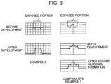
- FIG. 3 is refractive index distributions (before development and after development) of optical waveguides created in Example 3 and Comparative Example 1.
- a resin composition for optical waveguide cores is a resin composition containing liquid epoxy resin and solid epoxy resin, the coefficient of variation calculated from the weighted average value of the refractive index of the liquid epoxy resin and the refractive index of the solid epoxy resin being 2.10% or less.
- the fact that the coefficient of variation is 2.10% or less means that the differences in refractive index between all the epoxy resins contained in the resin composition are small, further the difference between the refractive index of the liquid epoxy resin and the refractive index of the solid epoxy resin is small, and accordingly the refractive index of the liquid epoxy resin and the average refractive index of the entire resin composition are almost approximately equal.
- the “refractive index” refers to the absolute refractive index and means a value obtained by dividing the propagation velocity of light in a vacuum by the propagation velocity of light in the substance, and is a value measured with an Abbe refractometer or the like.
- the refractive index of a liquid epoxy resin contained in the resin composition is denoted by R 1 n
- the parts by mass (ratio) of the liquid epoxy resin is by W 1 n
- the refractive index of a solid epoxy resin is by R 2 n
- the parts by mass of the solid epoxy resin is by W 2 n
- the average refractive index (Rav 1 ) of the liquid epoxy resins is calculated by Formula (1)
- the average refractive index (Rave) of the solid epoxy resins is by Formula (2)
- the average refractive index (Rav 3 ) of the entire resin composition is by Formula (3)
- the standard deviation (Std) calculated from the weighted average value of the refractive indices of the liquid epoxy resins contained in the resin composition and the refractive indices of the solid epoxy resins contained in the resin composition is by Formula (4)
- n represents an arbitrary integer; in the case where the resin composition contains, for example, n kinds of liquid epoxy resins, the refractive indices of them are written as R 1 1 , R 1 2 , . . . , and R 1 h .
- parts by mass is used for each formula in the present embodiment; however, in the case where there is substantially no difference between the densities of the epoxy resins, the parts by mass (weight fraction) may be replaced with parts by volume (volume fraction).
- the case where there is substantially no difference between the densities of the epoxy resins means that the difference in density is 0.3 g/cm 3 or less, preferably 0.04 g/cm 3 or less, and more preferably 0.02 g/cm 3 or less.
- Formulae (1) to (5) above may be derived from the refractive index of the one kind of epoxy resin; this similarly applies to the solid epoxy resin.
- the coefficient of variation is preferably 2.10% or less, more preferably 1.50% or less, still more preferably 1.00% or less, and most preferably 0.5% or less.
- the lower limit value of the coefficient of variation is ideally preferably 0%, but is in practice approximately 0.02%.
- the difference between the refractive index of an epoxy resin that is contained in the resin composition and has the highest refractive index and the refractive index of an epoxy resin that is contained in the resin composition and has the lowest refractive index is preferably 0.100 or less, more preferably 0.080 or less, still more preferably 0.040 or less, and most preferably 0.030 or less. Further, ideally it is preferable that the lower limit value be 0, but it is sufficient that the lower limit value be approximately 0.005. Thereby, a situation where a difference in refractive index occurs in the core after development can be suppressed more.
- the difference between the average refractive index of the liquid epoxy resin and the average refractive index of the entire resin composition that is, Rav 3 ⁇ Rav 1 is 0.04 or less, preferably 0.02 or less, and more preferably 0.01 or less.
- the lower limit value is ideally preferably 0, but is in practice approximately 0.0001. It is presumed that, by such a configuration, a situation where a difference in refractive index occurs in the core after development can be suppressed, and a uniform core with a clear width can be formed.
- Rav 3 may be replaced with the actual measurement value of the measured refractive index of the cured product of the resin composition of the present embodiment.
- Rav 2 ⁇ Rav 1 is preferably 0.07 or less, more preferably 0.04 or less, and still more preferably 0.02 or less. Further, the lower limit value is ideally preferably 0, but is in practice approximately 0.0001.
- the standard deviation (Std) of the resin composition according to the present embodiment is preferably 0.033 or less, more preferably 0.020 or less, and still more preferably 0.010 or less. Further, the lower limit value is ideally preferably 0, but is in practice approximately 0.001.
- any epoxy resin may be used without particular limitation as long as it is in a liquid form at normal temperature.
- Specific examples include bisphenol A type epoxy resins, bisphenol F type epoxy resins, hydrogenated bisphenol A type epoxy resins, hydrogenated bisphenol F type epoxy resins, alicyclic epoxy resins, biphenyl type epoxy resins, novolac type epoxy resins, trimethylolpropane type epoxy resins, polyethylene glycol type epoxy resins, and the like.
- CELLOXIDE 2021P manufactured by Daicel Corporation
- EX-201 manufactured by Nagase ChernteX Corporation
- EPICLON 850S manufactured by Dainippon Ink and Chemicals, Incorporated, and the like may be used.
- a plurality of liquid epoxy resins of two or more kinds are used, and it is desirable that the coefficient of variation calculated from the weighted average value of the refractive index of the liquid epoxy resin and the refractive index of the solid epoxy resin be 2.10% or less. It is presumed that, thereby, the area of dark portions formed during exposure is reduced more, and a core in which a situation where a difference in refractive index occurs in the core after development is suppressed and that has a clear, uniform width can be formed.
- the ratio of the liquid epoxy resin is 5 to 35 mass %, preferably 5 to 20 mass %, and still more preferably approximately 10 to 20 mass % to the entire resin composition. At such ratios, there is an advantage of being excellent in handleability when manufacturing a dry film for optical waveguides or the like.
- any epoxy resin may be used without particular limitation as long as it is in a solid form at normal temperature. It is preferable that the blending amount of the solid epoxy resin be adjusted so that the coefficient of variation calculated from the weighted average value of the refractive index of the liquid epoxy resin and the refractive index of the solid epoxy resin is 2.10% or less.
- alicyclic solid epoxy resins solid novolac type epoxy resins, bisphenol type epoxy resins, hydrogenated bisphenol type epoxy resins, and the like.
- Commercially available products may be used as these; for example, EHPE-3150 manufactured by Daicel Chemical Industries, Ltd., VG3101 manufactured by Printec Co., 1006FS manufactured by Mitsubishi Chemical Corporation, and the like may be used.
- the ratio of the solid epoxy resin is preferably approximately 65 to 95 mass % to the entire resin composition. At such ratios, there are advantages that the tackiness of the film before curing can be suppressed to a low level and powder falling, etc. during handling can be suppressed.
- the resin composition of the present embodiment may be composed of liquid epoxy resin and solid epoxy resin, but may contain resin components other than the above to the extent that the effect of the present invention is not impaired.
- the resin composition of the present embodiment may further contain a curing agent in addition to the epoxy resin described above.
- a photocuring agent that can start curing by light a photoacid generator that generates an acid by light, a photobase generator that generates a base by light, or the like
- a heat curing agent that can start curing by heat a heat acid generator that generates an acid by heat, a heat base generator that generates a base by heat, or the like
- a light heat curing agent that can start curing by each of light and heat, or the like may be used additionally.
- CPI101A (4-(diphenylsulfonio)diphenyl sulfide hexafluoroantimonate) and CPI200K (compound name: a triarylsulfonium salt type) manufactured by San-Apro Ltd.
- SI-150L an SbF6 type sulfonium salt manufactured by Sanshin Chemical Industry Co., Ltd., SP-170 manufactured by ADEKA Corporation, and the like may be used.
- SI-150L an SbF6 type sulfonium salt manufactured by Sanshin Chemical Industry Co., Ltd.
- SP-170 manufactured by ADEKA Corporation and the like may be used.
- These may be used singly, or may be used in combination of two or more kinds.
- the blending ratio of such a curing agent is, for example, preferably in the range of approximately 0.3 to 5 mass % to the total amount of the resin components in the resin composition.
- the blending ratio is 5 mass % or more, resin curing is allowed to be sufficient, and a hard cured product is obtained; however, if the amount of the curing agent is too large, cations or anions are generated excessively, and therefore there is a tendency that the composition for optical waveguides cures too easily, the shelf life of the composition for optical waveguides is reduced, and handleability is reduced, for example.
- an amount of 0.3 mass % or less is preferable because this does not cause the problems that curing distortion is likely to occur due to the curing agent being contained excessively, the cured product is embrittled due to increased amounts of the remaining acid or base and components that do not react with the cured product, etc.
- the resin composition for optical waveguide cores according to the present embodiment may further contain other additives, for example a curing promotion agent, a flame retardant agent, a flame retardant aid, a leveling agent, a coloring agent, etc., as necessary to the extent that the effect of the present invention is not impaired.
- additives for example a curing promotion agent, a flame retardant agent, a flame retardant aid, a leveling agent, a coloring agent, etc.
- the resin composition for optical waveguide cores of the present invention is usually prepared in a varnish form for use.
- a varnish is prepared in the following manner, for example.
- the varnish is obtained by selecting such a blending ratio that a substance obtained by the following process is in a solid form at normal temperature: the liquid and solid epoxy resins described above are dissolved in a solvent at a prescribed ratio and further a curing agent and, as necessary, other additives are blended, and the resulting varnish is dried to remove the solvent.
- the mixing ratio between the resin components and the solvent in the varnish is not particularly limited, and may be adjusted so as to obtain a viscosity suitable for application (putting) in a varnish state to a surface of a base material, as appropriate.
- the organic resolvent is not particularly limited, and examples include aromatic hydrocarbons such as benzene and toluene, amides such as N,N-dimethylformamide (DMF), ketones such as acetone and methyl ethyl ketone, and the like. These may be used singly, or may be used in combination of two or more kinds.
- aromatic hydrocarbons such as benzene and toluene
- amides such as N,N-dimethylformamide (DMF)
- ketones such as acetone and methyl ethyl ketone
- the temperature at the time of dissolution in the resolvent is approximately 50 to 100° C.
- a cured layer may be formed using a coating step of directly applying a varnish to a surface of a substrate and then performing drying; however, from the viewpoint of productivity, it is preferable to use a dry film that is formed from the resin composition described above in advance.
- a dry film that is formed from the resin composition described above in advance.
- optical waveguides can be manufactured with high productivity without needing a complicated coating step.
- a dry film there is also an advantage that an optical waveguide can be formed with uniform thickness accuracy.
- a dry film according to the present embodiment is formed by, for example, performing application to a surface of a film base material such as a PET film by using a multi coater of a comma coater head or the like and drying the workpiece. Further, a dry film with a thickness of approximately 10 to 100 ⁇ m can be obtained by performing thermal lamination using a polypropylene film or the like as a mold release film.
- a curable film for claddings and a curable film for cores are used in order to form a core and a cladding; in the present embodiment, a dry film made of the resin composition described above is used as the curing film for cores. Note that the refractive index of the curable film for claddings is adjusted so as to be lower than the refractive index of the curable film for cores.
- a surface of a substrate 10 on which an electric circuit 11 is formed is laminated with a curable film for claddings 1 , and then the curable film for claddings 1 is cured by performing light irradiation with ultraviolet rays or the like or heating.
- the substrate 10 for example, a flexible printed wiring board in which an electric circuit is formed on one surface of a transparent base material such as a polyimide film, a printed wiring board such as a glass epoxy, or the like is used.
- an undercladding 3 a is stacked and formed on the surface of the substrate 10 , as shown in FIG. 1 B .
- a surface of the undercladding 3 a is laminated with a curable film for cores 2 , then a mask in which slits of a core pattern are formed is superimposed, and light capable of making photocuring, such as ultraviolet rays, is applied through the slits; thereby, the photocurable film for cores 2 is exposed in the core pattern.
- a direct depiction system in which laser light is scanned and applied along a pattern configuration may be used as well as a method of using a mask to perform selective exposure.
- a curable film 1 for claddings is subjected to lamination and is stacked so as to cover the undercladding 3 a and the cores 4 . Then, the curable film 1 for claddings is cured by performing light irradiation or heating, and thereby an overcladding 3 b like that shown in FIG. 1 F is formed. In this way, an optical waveguide A in which the cores 4 are embedded in a cladding 3 composed of the undercladding 3 a and the overcladding 3 b is formed on the surface of the substrate 10 .
- the components were blended at the blending composition (parts by mass) shown in Table 1 below, and were mixed under refluxing while being heated at 80° C. Subsequently, distillation under reduced pressure was performed such that methyl ethyl ketone (MEK) accounted for 70 parts by mass relative to 100 parts by mass of the solid content. Next, filtration was performed with a membrane filter with a hole diameter of 1 ⁇ m, and then defoaming under reduced pressure was performed; thereby, an epoxy resin varnish was adjusted.
- MEK methyl ethyl ketone
- the varnish was applied to PET films (product number: A4100) manufactured by Toyobo Co., Ltd. by using a multi coater of a comma coater head manufactured by Hirano Tecseed Co., Ltd., and was dried to prescribed thicknesses, and OPP-MA420 manufactured by Oji F-Tex Co., Ltd., OPP-MA420 being a mold release film, was subjected to thermal lamination; thus, dry films with thicknesses of 10 ⁇ m and 50 ⁇ m were obtained.
- the average refractive index of the entire resin composition both a value (b) obtained by measuring the cured product of the resin composition with an Abbe refractometer DR-M2 manufactured by Atago Co., Ltd. and the average refractive index (Rav 3 ) calculated by the weighted average are written.
- the varnish was applied to a PET film (product number: A4100) manufactured by Toyobo Co., Ltd. by using a multi coater of a comma coater head manufactured by Hirano Tecseed Co., Ltd., and was dried; thus, a film with a prescribed thickness was obtained.
- film materials prepared in Examples 1 to 4 and Comparative Example 1 above were used as core materials.
- the curable film for claddings was used to perform lamination with a vacuum laminator “V-130” under conditions of 50° C. and 0.2 MPa. Then, the curable film for claddings was irradiated with ultraviolet light with an ultra-high pressure mercury lamp under a condition of 2 J/cm 2 , and further the mold release film was peeled off; then, heat treatment was performed at 140° C. for 30 minutes, and further oxygen plasma treatment was performed; thus, an undercladding in which the curable film for claddings was cured was formed.
- FIG. 2 Cross-sectional photographs before development and after development of the cores manufactured using the materials for cores of Examples 1 to 4 and Comparative Example 1 are shown in FIG. 2 (for Example 4, only a cross-sectional photograph after development).
- Example 3 and Comparative Example 1 the refractive index distribution of the core layer was measured using a quantitative phase microscope.
- the vertical axis in the drawing of Example 3 represents the refractive index
- the horizontal axis represents the distance (for showing the width of the core)
- 1 graduation of the vertical axis is 0.010.
- similarly 1 graduation of the vertical axis is 0.015 (not shown).
- FIG. 3 shows refractive index distributions before development (after exposure) and after development in Example 3 and Comparative Example 1. From this drawing, it can be seen that, in Example 3, places where the refractive index is lower than in a central portion of the exposed portion by approximately 0.05 were formed in side portions of the exposed portion before development; on the other hand, in Comparative Example 1, layers in which the refractive index is lower than in a central portion by approximately 0.015 were formed in side portions of the exposed portion.
- Example 3 the refractive index in the core after development is substantially fixed (uniform) from the side portions to the central portion; on the other hand, in Comparative Example 1, there are parts where the refractive index varies by 0.015 or more at the maximum, and the refractive index is not uniform.
- the present invention has wide-ranging industrial applicability in technical fields regarding optical waveguides and photoelectric composite wiring boards.
Abstract
Description
- Patent Literature 1: JP 2012-128360 A
[Math. 5]
C.V.=Std/Rav3×100(%) (5)
-
- “CELLOXIDE 2021P (CEL2021P)”: manufactured by Daicel Corporation (refractive index; 1.5175; viscosity: 250 mPa·s)
- “EX-321L”: manufactured by Nagase ChemteX Corporation (refractive index: 1.5069; viscosity: 300 mPa·s)
- “EX-201”: manufactured by Nagase ChemteX Corporation (refractive index: 1.5799; viscosity: 250 mPa·s)
- “EPICLON 850S”: manufactured by DIC Corporation (refractive index: 1.5859; viscosity: 13,000)
-
- “EHPE3150”: manufactured by Daicel Corporation, an alicyclic epoxy (refractive index: 1.5199)
- “VG3101”: manufactured by Printec Co., a monomer type triphenylmethane type epoxy resin (refractive index: 1.6022)
- “EPIKOTE 1006FS”: manufactured by Mitsubishi Chemical Corporation, a bisphenol A type epoxy resin (refractive index: 1.5948)
-
- “SP-170”: (manufactured by ADEKA Corporation)
-
- “PF636”: (manufactured by OMNOVA) a leveling agent
- “AO-60”: manufactured by ADEKA Corporation, an antioxidant
| TABLE 1 | ||||||||
| Refractive | Comparative | |||||||
| index | Nature | Viscosity | Example 1 | Example 2 | Example 3 | Example 4 | Example 1 | |
| CEL2021P | 1.5175 | Liquid | 250 | 0 | 0 | 3 | 0 | 23 |
| EX32IL | 1.5069 | Liquid | 300 | 0 | 0 | 0 | 6 | 0 |
| EX20I | 1.5799 | Liquid | 250 | 0 | 23 | 0 | 0 | 0 |
| 850S | 1.5859 | Liquid | 13000 | 23 | 0 | 13 | 17 | 0 |
| EHPE3150 | 1.5199 | Solid | — | 0 | 0 | 24 | 0 | 0 |
| VG3101L | 1.6022 | Solid | — | 21 | 21 | 0 | 0 | 21 |
| 1006FS | 1.5948 | Solid | — | 56 | 56 | 60 | 77 | 56 |
| Curing agent SP-170 | 0.6 | 0.6 | 0.6 | 0.6 | 0.6 | |||
| Antioxidant AO-60 | 0.3 | 0.3 | 0.3 | 0.3 | 0.3 | |||
| Leveling agent PF-636 | 0.1 | 0.1 | 0.1 | 0.1 | 0.1 | |||
| Liquid/solid | 23/77 | 23/77 | 16/84 | 23/77 | 23/77 | |||
| Refractive index of liquid | 1.5859 | 1.5799 | 1.5731 | 1.5653 | 1.5175 | |||
| content a (Rav1) | ||||||||
| Refractive index of entire | 1.5943 | 1.5929 | 1.5733 | 1.588 | 1.5786 | |||
| core b (actual measurement) | ||||||||
| b-a | 0.0084 | 0.0130 | 0.0002 | 0.0227 | 0.0611 | |||
| Rav3 | 1.5943 | 1.5929 | 1.5733 | 1.5880 | 1.5786 | |||
| Rav2 | 1.5968 | 1.5968 | 1.5734 | 1.5948 | 1.5968 | |||
| Rav3-Rav1 | 0.0084 | 0.0130 | 0.0002 | 0.0227 | 0.0611 | |||
| Rav2-Rav1 | 0.0109 | 0.0169 | 0.0003 | 0.0295 | 0.0793 | |||
| Std | 0.005 | 0.008 | 0.033 | 0.021 | 0.034 | |||
| C.V. [%] | 0.34 | 0.48 | 2.08 | 1.31 | 2.12 | |||
| Highest refractive index- | 0.0163 | 0.0223 | 0.0773 | 0.0879 | 0.0847 | |||
| lowest refractive index | ||||||||
Claims (8)
Applications Claiming Priority (4)
| Application Number | Priority Date | Filing Date | Title |
|---|---|---|---|
| JP2017199544 | 2017-10-13 | ||
| JPJP2017-199544 | 2017-10-13 | ||
| JP2017-199544 | 2017-10-13 | ||
| PCT/JP2018/037842 WO2019074035A1 (en) | 2017-10-13 | 2018-10-11 | Resin composition for optical waveguide cores, and dry film, optical waveguide core and photoelectric composite wiring board, each of which uses same |
Publications (2)
| Publication Number | Publication Date |
|---|---|
| US20210221999A1 US20210221999A1 (en) | 2021-07-22 |
| US11680163B2 true US11680163B2 (en) | 2023-06-20 |
Family
ID=66100065
Family Applications (1)
| Application Number | Title | Priority Date | Filing Date |
|---|---|---|---|
| US16/755,284 Active 2040-02-26 US11680163B2 (en) | 2017-10-13 | 2018-10-11 | Resin composition for optical waveguide cores, and dry film, optical waveguide core and photoelectric composite wiring board, each of which uses same |
Country Status (5)
| Country | Link |
|---|---|
| US (1) | US11680163B2 (en) |
| JP (1) | JPWO2019074035A1 (en) |
| CN (1) | CN111201460A (en) |
| TW (1) | TW201922912A (en) |
| WO (1) | WO2019074035A1 (en) |
Citations (8)
| Publication number | Priority date | Publication date | Assignee | Title |
|---|---|---|---|---|
| JP2005221556A (en) | 2004-02-03 | 2005-08-18 | Nitto Denko Corp | Optical waveguide manufacturing method |
| TW200621817A (en) | 2004-10-07 | 2006-07-01 | Hitachi Chemical Co Ltd | Resin composition for optical material, resin film for optical material and optical waveguide using the same |
| CN101220200A (en) | 2007-12-20 | 2008-07-16 | 上海交通大学 | Transparent organic polymer material and method for producing the same |
| US20090062421A1 (en) | 2006-03-15 | 2009-03-05 | Hitachi Cheimical Company Ltd. | Phenoxy Resin for Optical Material, Resin Composition for Optical Material, Resin Film For Optical Material and Optical Waveguide Using Those |
| JP2009104084A (en) | 2007-10-25 | 2009-05-14 | Panasonic Electric Works Co Ltd | Light guide and photoelectric compound panel |
| JP2012128360A (en) | 2010-12-17 | 2012-07-05 | Hitachi Chem Co Ltd | Resin composition for optical material, resin film for optical material, varnish for optical material and optical waveguide using the same |
| US8532442B2 (en) * | 2009-03-26 | 2013-09-10 | Panasonic Corporation | Optical waveguide-forming epoxy resin composition, optical waveguide-forming curable film, optical-transmitting flexible printed circuit, and electronic information device |
| WO2017038040A1 (en) | 2015-09-01 | 2017-03-09 | パナソニックIpマネジメント株式会社 | Composition for optical waveguide, dry film for optical waveguide and optical waveguide |
-
2018
- 2018-10-11 JP JP2019548227A patent/JPWO2019074035A1/en active Pending
- 2018-10-11 WO PCT/JP2018/037842 patent/WO2019074035A1/en active Application Filing
- 2018-10-11 US US16/755,284 patent/US11680163B2/en active Active
- 2018-10-11 CN CN201880065913.8A patent/CN111201460A/en active Pending
- 2018-10-12 TW TW107136045A patent/TW201922912A/en unknown
Patent Citations (13)
| Publication number | Priority date | Publication date | Assignee | Title |
|---|---|---|---|---|
| JP2005221556A (en) | 2004-02-03 | 2005-08-18 | Nitto Denko Corp | Optical waveguide manufacturing method |
| US20100266258A1 (en) | 2004-07-10 | 2010-10-21 | Tomoaki Shibata | Resin composition for optical material, resin film for optical material and optical waveguide using same |
| TW200621817A (en) | 2004-10-07 | 2006-07-01 | Hitachi Chemical Co Ltd | Resin composition for optical material, resin film for optical material and optical waveguide using the same |
| US20080260341A1 (en) | 2004-10-07 | 2008-10-23 | Tomoaki Shibata | Resin Composition for Optical Material, Resin Film for Optical Material and Optical Waveguide Using Same |
| US20090062421A1 (en) | 2006-03-15 | 2009-03-05 | Hitachi Cheimical Company Ltd. | Phenoxy Resin for Optical Material, Resin Composition for Optical Material, Resin Film For Optical Material and Optical Waveguide Using Those |
| CN101400719A (en) | 2006-03-15 | 2009-04-01 | 日立化成工业株式会社 | Phenoxy resin for optical material, resin composition for optical material, resin film for optical material, and optical waveguide using those |
| JP2009104084A (en) | 2007-10-25 | 2009-05-14 | Panasonic Electric Works Co Ltd | Light guide and photoelectric compound panel |
| CN101220200A (en) | 2007-12-20 | 2008-07-16 | 上海交通大学 | Transparent organic polymer material and method for producing the same |
| US8532442B2 (en) * | 2009-03-26 | 2013-09-10 | Panasonic Corporation | Optical waveguide-forming epoxy resin composition, optical waveguide-forming curable film, optical-transmitting flexible printed circuit, and electronic information device |
| JP2012128360A (en) | 2010-12-17 | 2012-07-05 | Hitachi Chem Co Ltd | Resin composition for optical material, resin film for optical material, varnish for optical material and optical waveguide using the same |
| WO2017038040A1 (en) | 2015-09-01 | 2017-03-09 | パナソニックIpマネジメント株式会社 | Composition for optical waveguide, dry film for optical waveguide and optical waveguide |
| US20180224604A1 (en) | 2015-09-01 | 2018-08-09 | Panasonic Intellectual Property Management Co., Ltd. | Composition for optical waveguide, dry film for optical waveguide and optical waveguide |
| US20190212495A1 (en) | 2015-09-01 | 2019-07-11 | Panasonic Intellectual Property Management Co., Ltd. | Composition for optical waveguide, dry film for optical waveguide and optical waveguide using epoxies |
Non-Patent Citations (1)
| Title |
|---|
| Official Communication issued in International Bureau of WIPO Patent Application No. PCT/2018/037842, dated Dec. 4, 2018. |
Also Published As
| Publication number | Publication date |
|---|---|
| US20210221999A1 (en) | 2021-07-22 |
| WO2019074035A1 (en) | 2019-04-18 |
| CN111201460A (en) | 2020-05-26 |
| JPWO2019074035A1 (en) | 2020-12-03 |
| TW201922912A (en) | 2019-06-16 |
Similar Documents
| Publication | Publication Date | Title |
|---|---|---|
| KR20070108354A (en) | Resin composition for optical material, resin film for optical material and optical waveguide using same | |
| EP2639251B1 (en) | Optical waveguide forming epoxy resin composition, curable film formed from the epoxy resin composition for formation of optical waveguide, and light transmission flexible printed board | |
| CN105102500B (en) | Photosensitive epoxy resin composition for optical waveguide, curable film for forming optical waveguide, optical waveguide and mixed flexible printed wiring board for optical/electrical transmission using same, and method for producing optical waveguide | |
| KR102109228B1 (en) | Photosensitive epoxy resin composition, curable film for formation of optical waveguide core layer, and optical waveguide and optical/electrical transmission hybrid flexible printed wiring board produced by using the photosensitive epoxy resin composition or the curable film | |
| KR20130120384A (en) | Optical waveguide forming epoxy resin composition, curable film for formation of optical waveguide, and light transmission flexible printed board, and method for producing the same | |
| KR102605384B1 (en) | Photosensitive resin composition for optical waveguide and photocurable film for forming optical waveguide core layer, and optical waveguide and light/electricity transmission hybrid flexible printed wiring board using same | |
| KR102419966B1 (en) | Photosensitive epoxy resin composition for optical waveguide formation, curable film for optical waveguide formation and optical waveguide using same, mixed flexible printed wiring board for optical and electrical transmission | |
| KR102641200B1 (en) | A photosensitive epoxy resin composition for forming an optical waveguide and a photosensitive film for forming an optical waveguide, and an optical waveguide manufactured using the epoxy resin composition or the photosensitive film, and a mixed flexible printed wiring board for optical and electrical transmission | |
| US11680163B2 (en) | Resin composition for optical waveguide cores, and dry film, optical waveguide core and photoelectric composite wiring board, each of which uses same | |
| JP6332590B2 (en) | Photosensitive resin composition for optical waveguide, photocurable film for forming optical waveguide core layer, optical waveguide using the same, mixed flexible printed wiring board for optical / electrical transmission | |
| KR102312851B1 (en) | Photosensitive resin composition for optical waveguide and photocurable film for formation of optical waveguide core layer, as well as optical waveguide using same and mixed-mounting flexible printed wiring board for optical and electrical transmission | |
| JP7224802B2 (en) | Photosensitive epoxy resin composition for forming optical waveguides, photosensitive film for forming optical waveguides, optical waveguides using the same, hybrid flexible printed wiring boards for optical/electrical transmission | |
| US10324255B2 (en) | Photosensitive epoxy resin composition for formation of optical waveguide | |
| JP4929667B2 (en) | Resin composition for optical material, resin film for optical material, and optical waveguide using the same | |
| US9989848B2 (en) | Photosensitive resin composition for optical waveguide, photocurable film for formation of optical waveguide core layer, optical waveguide produced by using the resin composition or the photocurable film, and hybrid flexible printed wiring board for optical/electrical transmission | |
| WO2023276622A1 (en) | Resin composition for optical waveguide, and dry film and optical waveguide using same | |
| KR20140064640A (en) | Resin composition for forming optical waveguide, optical waveguide using the resin composition, light transmission flexible printed board, and method for producing the optical waveguide | |
| EP2189826A1 (en) | Method for manufacturing optical waveguide and optical waveguide manufactured by the method |
Legal Events
| Date | Code | Title | Description |
|---|---|---|---|
| FEPP | Fee payment procedure |
Free format text: ENTITY STATUS SET TO UNDISCOUNTED (ORIGINAL EVENT CODE: BIG.); ENTITY STATUS OF PATENT OWNER: LARGE ENTITY |
|
| AS | Assignment |
Owner name: PANASONIC INTELLECTUAL PROPERTY MANAGEMENT CO., LTD., JAPAN Free format text: ASSIGNMENT OF ASSIGNORS INTEREST;ASSIGNORS:KURIZOE, JUNKO;KONDOU, NAOYUKI;NAKASHIBA, TORU;AND OTHERS;REEL/FRAME:053032/0541 Effective date: 20200324 |
|
| STPP | Information on status: patent application and granting procedure in general |
Free format text: APPLICATION DISPATCHED FROM PREEXAM, NOT YET DOCKETED |
|
| STPP | Information on status: patent application and granting procedure in general |
Free format text: DOCKETED NEW CASE - READY FOR EXAMINATION |
|
| STPP | Information on status: patent application and granting procedure in general |
Free format text: NON FINAL ACTION MAILED |
|
| STPP | Information on status: patent application and granting procedure in general |
Free format text: RESPONSE TO NON-FINAL OFFICE ACTION ENTERED AND FORWARDED TO EXAMINER |
|
| STPP | Information on status: patent application and granting procedure in general |
Free format text: FINAL REJECTION MAILED |
|
| STCF | Information on status: patent grant |
Free format text: PATENTED CASE |