US11653564B2 - Compound and organic light-emitting device comprising same - Google Patents
Compound and organic light-emitting device comprising same Download PDFInfo
- Publication number
- US11653564B2 US11653564B2 US16/322,065 US201716322065A US11653564B2 US 11653564 B2 US11653564 B2 US 11653564B2 US 201716322065 A US201716322065 A US 201716322065A US 11653564 B2 US11653564 B2 US 11653564B2
- Authority
- US
- United States
- Prior art keywords
- compound
- group
- chemical formula
- light emitting
- layer
- Prior art date
- Legal status (The legal status is an assumption and is not a legal conclusion. Google has not performed a legal analysis and makes no representation as to the accuracy of the status listed.)
- Active, expires
Links
Images


Classifications
-
- C—CHEMISTRY; METALLURGY
- C07—ORGANIC CHEMISTRY
- C07D—HETEROCYCLIC COMPOUNDS
- C07D471/00—Heterocyclic compounds containing nitrogen atoms as the only ring hetero atoms in the condensed system, at least one ring being a six-membered ring with one nitrogen atom, not provided for by groups C07D451/00 - C07D463/00
- C07D471/02—Heterocyclic compounds containing nitrogen atoms as the only ring hetero atoms in the condensed system, at least one ring being a six-membered ring with one nitrogen atom, not provided for by groups C07D451/00 - C07D463/00 in which the condensed system contains two hetero rings
- C07D471/04—Ortho-condensed systems
-
- C—CHEMISTRY; METALLURGY
- C07—ORGANIC CHEMISTRY
- C07D—HETEROCYCLIC COMPOUNDS
- C07D311/00—Heterocyclic compounds containing six-membered rings having one oxygen atom as the only hetero atom, condensed with other rings
- C07D311/02—Heterocyclic compounds containing six-membered rings having one oxygen atom as the only hetero atom, condensed with other rings ortho- or peri-condensed with carbocyclic rings or ring systems
- C07D311/78—Ring systems having three or more relevant rings
- C07D311/80—Dibenzopyrans; Hydrogenated dibenzopyrans
-
- C—CHEMISTRY; METALLURGY
- C07—ORGANIC CHEMISTRY
- C07D—HETEROCYCLIC COMPOUNDS
- C07D405/00—Heterocyclic compounds containing both one or more hetero rings having oxygen atoms as the only ring hetero atoms, and one or more rings having nitrogen as the only ring hetero atom
- C07D405/02—Heterocyclic compounds containing both one or more hetero rings having oxygen atoms as the only ring hetero atoms, and one or more rings having nitrogen as the only ring hetero atom containing two hetero rings
- C07D405/10—Heterocyclic compounds containing both one or more hetero rings having oxygen atoms as the only ring hetero atoms, and one or more rings having nitrogen as the only ring hetero atom containing two hetero rings linked by a carbon chain containing aromatic rings
-
- C—CHEMISTRY; METALLURGY
- C07—ORGANIC CHEMISTRY
- C07D—HETEROCYCLIC COMPOUNDS
- C07D405/00—Heterocyclic compounds containing both one or more hetero rings having oxygen atoms as the only ring hetero atoms, and one or more rings having nitrogen as the only ring hetero atom
- C07D405/14—Heterocyclic compounds containing both one or more hetero rings having oxygen atoms as the only ring hetero atoms, and one or more rings having nitrogen as the only ring hetero atom containing three or more hetero rings
-
- H—ELECTRICITY
- H10—SEMICONDUCTOR DEVICES; ELECTRIC SOLID-STATE DEVICES NOT OTHERWISE PROVIDED FOR
- H10K—ORGANIC ELECTRIC SOLID-STATE DEVICES
- H10K50/00—Organic light-emitting devices
-
- H—ELECTRICITY
- H10—SEMICONDUCTOR DEVICES; ELECTRIC SOLID-STATE DEVICES NOT OTHERWISE PROVIDED FOR
- H10K—ORGANIC ELECTRIC SOLID-STATE DEVICES
- H10K50/00—Organic light-emitting devices
- H10K50/10—OLEDs or polymer light-emitting diodes [PLED]
-
- H—ELECTRICITY
- H10—SEMICONDUCTOR DEVICES; ELECTRIC SOLID-STATE DEVICES NOT OTHERWISE PROVIDED FOR
- H10K—ORGANIC ELECTRIC SOLID-STATE DEVICES
- H10K50/00—Organic light-emitting devices
- H10K50/10—OLEDs or polymer light-emitting diodes [PLED]
- H10K50/14—Carrier transporting layers
- H10K50/16—Electron transporting layers
-
- H—ELECTRICITY
- H10—SEMICONDUCTOR DEVICES; ELECTRIC SOLID-STATE DEVICES NOT OTHERWISE PROVIDED FOR
- H10K—ORGANIC ELECTRIC SOLID-STATE DEVICES
- H10K85/00—Organic materials used in the body or electrodes of devices covered by this subclass
- H10K85/60—Organic compounds having low molecular weight
- H10K85/649—Aromatic compounds comprising a hetero atom
- H10K85/654—Aromatic compounds comprising a hetero atom comprising only nitrogen as heteroatom
-
- H—ELECTRICITY
- H10—SEMICONDUCTOR DEVICES; ELECTRIC SOLID-STATE DEVICES NOT OTHERWISE PROVIDED FOR
- H10K—ORGANIC ELECTRIC SOLID-STATE DEVICES
- H10K85/00—Organic materials used in the body or electrodes of devices covered by this subclass
- H10K85/60—Organic compounds having low molecular weight
- H10K85/649—Aromatic compounds comprising a hetero atom
- H10K85/657—Polycyclic condensed heteroaromatic hydrocarbons
- H10K85/6572—Polycyclic condensed heteroaromatic hydrocarbons comprising only nitrogen in the heteroaromatic polycondensed ring system, e.g. phenanthroline or carbazole
-
- H—ELECTRICITY
- H10—SEMICONDUCTOR DEVICES; ELECTRIC SOLID-STATE DEVICES NOT OTHERWISE PROVIDED FOR
- H10K—ORGANIC ELECTRIC SOLID-STATE DEVICES
- H10K85/00—Organic materials used in the body or electrodes of devices covered by this subclass
- H10K85/60—Organic compounds having low molecular weight
- H10K85/649—Aromatic compounds comprising a hetero atom
- H10K85/657—Polycyclic condensed heteroaromatic hydrocarbons
- H10K85/6574—Polycyclic condensed heteroaromatic hydrocarbons comprising only oxygen in the heteroaromatic polycondensed ring system, e.g. cumarine dyes
-
- H—ELECTRICITY
- H10—SEMICONDUCTOR DEVICES; ELECTRIC SOLID-STATE DEVICES NOT OTHERWISE PROVIDED FOR
- H10K—ORGANIC ELECTRIC SOLID-STATE DEVICES
- H10K99/00—Subject matter not provided for in other groups of this subclass
-
- H—ELECTRICITY
- H10—SEMICONDUCTOR DEVICES; ELECTRIC SOLID-STATE DEVICES NOT OTHERWISE PROVIDED FOR
- H10K—ORGANIC ELECTRIC SOLID-STATE DEVICES
- H10K50/00—Organic light-emitting devices
- H10K50/10—OLEDs or polymer light-emitting diodes [PLED]
- H10K50/17—Carrier injection layers
- H10K50/171—Electron injection layers
Definitions
- An organic light emitting device has a structure in which an organic thin film is disposed between two electrodes. When a voltage is applied to an organic light emitting device having the structure, electrons and holes injected from the two electrodes are bonded to each other in an organic thin film to make a pair, and then emit light while being extinguished.
- the organic thin film may be composed of a single layer or multi layers, if necessary.
- a material for the organic thin film may have a light emitting function, if necessary.
- a material for the organic thin film it is also possible to use a compound, which may itself constitute a light emitting layer alone, or it is also possible to use a compound, which may serve as a host or a dopant of a host-dopant-based light emitting layer.
- a compound for the organic thin film it is also possible to use a compound, which may perform a function such as hole injection, hole transport, electron blocking, hole blocking, electron transport or electron injection.
- the present specification provides a compound and an organic light emitting device including the same.
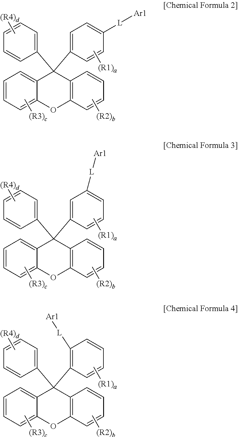
- An exemplary embodiment of the present specification provides a compound represented by the following Chemical Formula 1.
- Ar's are the same as or different from each other, and are each independently -L-Ar1,
- R1 to R4 are the same as or different from each other, and are each independently hydrogen or deuterium
- a, b, and c are an integer from 0 to 4
- n is an integer from 1 to 4
- d is an integer from 0 to 5
- n+a is 5 or less
- substituents in the parenthesis are the same as or different from each other
- L is a direct bond; or a substituted or unsubstituted arylene group,
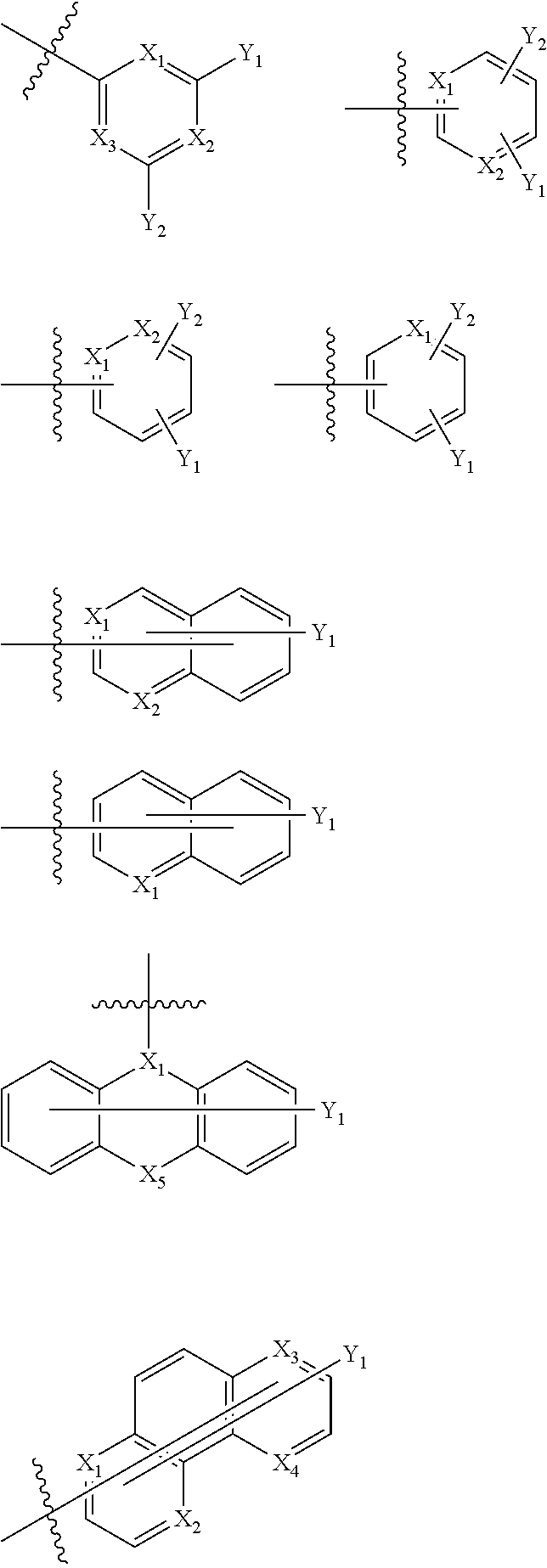
- Ar1 is selected from the following structural formulae,
- X 1 to X 4 are the same as or different from each other, and are each independently N or CH, and X 5 is S or O, and
- Y 1 and Y 2 are the same as or different from each other, and are each independently hydrogen; deuterium; a nitrile group; a substituted or unsubstituted alkyl group; a substituted or unsubstituted aryl group; a substituted or unsubstituted heteroaryl group; or a substituted or unsubstituted fused polycyclic group.
- an organic light emitting device including: a first electrode; a second electrode disposed to face the first electrode; and an organic material layer having one or more layers disposed between the first electrode and the second electrode, in which one or more layers of the organic material layer include the above-described compound.
- the compound according to an exemplary embodiment of the present application is used for an organic light emitting device and thus may lower the driving voltage of the organic light emitting device, and improve the light efficiency, and service life characteristics of the device by thermal stability of the compound.
- FIG. 1 illustrates an example of an organic light emitting device in which a substrate 1 , a positive electrode 2 , a light emitting layer 3 , and a negative electrode 4 are sequentially stacked.
- FIG. 2 illustrates an example of an organic light emitting device in which a substrate 1 , a positive electrode 2 , a hole injection layer 5 , a hole transporting layer 6 , a light emitting layer 3 , an electron transporting layer 7 , and a negative electrode 4 are sequentially stacked.
- FIG. 3 illustrates a HOMO energy level of Compound E1 according to an exemplary embodiment of the present specification, which is measured by using a photoelectron spectrometer.
- FIG. 4 illustrates a HOMO energy level of Compound E3 according to an exemplary embodiment of the present specification, which is measured by using a photoelectron spectrometer.
- FIG. 5 illustrates a HOMO energy level of Compound [ET-1-J], which is measured by using a photoelectron spectrometer.
- FIG. 6 is absorption and emission spectra of Compound E1 according to an exemplary embodiment of the present specification, which are measured via photoluminescence (PL).
- FIG. 7 is absorption and emission spectra of Compound E3 according to an exemplary embodiment of the present specification, which are measured via photoluminescence (PL).
- FIG. 8 is absorption and emission spectra of Compound [ET-1-J], which are measured via photoluminescence (PL).
- a dotted line mean a site bonded to another substituent or a binding portion.
- substitution means that a hydrogen atom bonded to a carbon atom of a compound is changed into another substituent, and a position to be substituted is not limited as long as the position is a position at which the hydrogen atom is substituted, that is, a position at which the substituent may be substituted, and when two or more are substituted, the two or more substituents may be the same as or different from each other.
- substituted or unsubstituted means being substituted with one or two or more substituents selected from the group consisting of deuterium; a halogen group; a cyano group; a nitro group; a hydroxy group; an alkyl group; a cycloalkyl group; an alkenyl group; an alkoxy group; a substituted or unsubstituted phosphine oxide group; an aryl group; and a heteroaryl group, being substituted with a substituent to which two or more substituents among the exemplified substituents are linked, or having no substituent.
- the substituent to which two or more substituents are linked may be a biphenyl group. That is, the biphenyl group may also be an aryl group, and may be interpreted as a substituent to which two phenyl groups are linked.
- examples of a halogen group include fluorine, chlorine, bromine or iodine.
- the alkyl group may be straight or branched, and the number of carbon atoms thereof is not particularly limited, but is preferably 1 to 50. Specific examples thereof include methyl, ethyl, propyl, n-propyl, isopropyl, butyl, n-butyl, isobutyl, tert-butyl, sec-butyl, 1-methyl-butyl, 1-ethyl-butyl, pentyl, n-pentyl, isopentyl, neopentyl, tert-pentyl, hexyl, n-hexyl, 1-methylpentyl, 2-methylpentyl, 4-methyl-2-pentyl, 3,3-dimethylbutyl, 2-ethylbutyl, heptyl, n-heptyl, 1-methylhexyl, cyclopentylmethyl, cyclohexylmethyl, octyl,
- a cycloalkyl group is not particularly limited, but the number of carbon atoms thereof is preferably 3 to 60, and specific examples thereof include cyclopropyl, cyclobutyl, cyclopentyl, 3-methylcyclopentyl, 2,3-dimethylcyclopentyl, cyclohexyl, 3-methylcyclohexyl, 4-methylcyclohexyl, 2,3-dimethylcyclohexyl, 3,4,5-trimethylcyclohexyl, 4-tert-butylcyclohexyl, cycloheptyl, cyclooctyl, and the like, but are not limited thereto.
- the alkoxy group may be straight, branched, or cyclic.
- the number of carbon atoms of the alkoxy group is not particularly limited, but is preferably 1 to 20. Specific examples thereof include methoxy, ethoxy, n-propoxy, isopropoxy, i-propyloxy, n-butoxy, isobutoxy, tert-butoxy, sec-butoxy, n-pentyloxy, neopentyloxy, isopentyloxy, n-hexyloxy, 3,3-dimethylbutyloxy, 2-ethylbutyloxy, n-octyloxy, n-nonyloxy, n-decyloxy, benzyloxy, p-methylbenzyloxy, and the like, but are not limited thereto.
- the alkenyl group may be straight or branched, and the number of carbon atoms thereof is not particularly limited, but is preferably 2 to 40.
- Specific examples thereof include vinyl, 1-propenyl, isopropenyl, 1-butenyl, 2-butenyl, 3-butenyl, 1-pentenyl, 2-pentenyl, 3-pentenyl, 3-methyl-1-butenyl, 1,3-butadienyl, allyl, 1-phenylvinyl-1-yl, 2-phenylvinyl-1-yl, 2,2-diphenylvinyl-1-yl, 2-phenyl-2-(naphthyl-1-yl)vinyl-1-yl, 2,2-bis(diphenyl-1-yl)vinyl-1-yl, a stilbenyl group, a styrenyl group, and the like, but are not limited thereto.
- phosphine oxide group examples include a diphenylphosphine oxide group, dinaphthylphosphine oxide group, and the like, but are not limited thereto.
- the aryl group is a monocyclic aryl group
- the number of carbon atoms thereof is not particularly limited, but is preferably 6 to 30.
- Specific examples of the monocyclic aryl group include a phenyl group, a biphenyl group, a terphenyl group, and the like, but are not limited thereto.
- the aryl group is a polycyclic aryl group
- the number of carbon atoms thereof is not particularly limited, but is preferably 10 to 24.
- Specific examples of the polycyclic aryl group include a naphthyl group, an anthracenyl group, a phenanthryl group, a pyrenyl group, a perylenyl group, a chrysenyl group, a fluorenyl group, and the like, but are not limited thereto.
- the fluorenyl group may be substituted, and adjacent substituents may be bonded to each other to form a ring.
- the group may be any organic compound.
- the group may be any organic compound.
- a heteroaryl group includes one or more atoms other than carbon, that is, one or more heteroatoms, and specifically, the heteroatom may include one or more atoms selected from the group consisting of O, N, Se, and S, and the like.
- the number of carbon atoms of the heteroaryl group is not particularly limited, but is preferably 2 to 60 or 2 to 30.
- heteroaryl group examples include a thiophenyl group, a furanyl group, a pyrrole group, an imidazolyl group, a thiazolyl group, an oxazolyl group, an oxadiazolyl group, a triazolyl group, a pyridyl group, a bipyridyl group, a pyrimidyl group, a triazinyl group, an acridyl group, a hydroacridyl group (for example,
- a pyridazinyl group a pyrazinyl group, a quinolinyl group, a quinazolinyl group, a quinoxalinyl group, a phthalazinyl group, a pyridopyrimidinyl group, a pyridopyrazinyl group, a pyrazinopyrazinyl group, an isoquinolinyl group, an indole group, a carbazolyl group, a benzoxazolyl group, a benzimidazolyl group, a benzothiazolyl group, a benzocarbazolyl group, a dibenzocarbazolyl group, a benzothiophenyl group, a dibenzothiophenyl group, a benzofuranyl group, a dibenzofuranyl group; a benzosilole group; a dibenzosilole group; a phenanthroliny
- a fused heterocyclic group may be a fused ring of an aromatic ring and an aliphatic ring, and may be selected from the examples of the heteroaryl group.
- aryl group may be applied to an arylene except for a divalent arylene group.
- n 1
- Chemical Formula 1 is represented by any one of the following Chemical Formulae 2 to 4.
- R1 to R4 a to d, L, and Ar1 are the same as the definitions in Chemical Formula 1.
- L is a direct bond
- L is an arylene group.
- L is an arylene group having 6 to 30 carbon atoms.
- L is a monocyclic arylene group.
- L is a direct bond; a phenylene group; a biphenylylene group; or a terphenylylene group.
- L is a direct bond; a phenylene group; or a biphenylylene group.
- L is selected from a direct bond or the following structural formulae.
- a dotted line means a bonding position in which Chemical Formula 1 is bonded to Ar1.
- R1 to R4 are hydrogen.
- Ar1 is selected from the following structural formulae.
- X 1 to X 4 are the same as or different from each other, and are each independently N or CH, and X 5 is S or O, and
- Y 1 and Y 2 are the same as or different from each other, and are each independently hydrogen; deuterium; a nitrile group; a substituted or unsubstituted alkyl group; a substituted or unsubstituted aryl group; a substituted or unsubstituted heteroaryl group; or a substituted or unsubstituted fused polycyclic group.
- a wavy line means a position which is bonded to L.
- Ar1 includes at least one N, or has a nitrile group as a substituent.
- At least one of X1 to X4 of Ar1 is N, and when X1 to X4 are all CH, Y1 or Y2 is a nitrile group.
- Ar1 is the substituent, there is an excellent effect by forming HOMO and LUMO levels at low levels to smoothly transport electrons and block holes.
- Y 1 and Y 2 are the same as or different from each other, and are each independently hydrogen; deuterium; a nitrile group; a substituted or unsubstituted aryl group; or a substituted or unsubstituted heteroaryl group.
- Y 1 and Y 2 are the same as or different from each other, and are each independently hydrogen; deuterium; a nitrile group; a substituted or unsubstituted aryl group having 6 to 30 carbon atoms; or a substituted or unsubstituted heteroaryl group having 2 to 30 carbon atoms.
- Y 1 and Y 2 are the same as or different from each other, and are each independently hydrogen; deuterium; a nitrile group; a substituted or unsubstituted phenyl group; a substituted or unsubstituted biphenyl group; a substituted or unsubstituted naphthyl group; a substituted or unsubstituted phenanthryl group; a substituted or unsubstituted pyridine group; or a substituted or unsubstituted dibenzofuranyl group.
- Y 1 and Y 2 are the same as or different from each other, and are each independently hydrogen; deuterium; a nitrile group; a phenyl group; a biphenyl group; a naphthyl group; a phenanthryl group; a pyridine group; or a dibenzofuranyl group.
- Ar1 is selected from the following structural formulae.
- a dotted line means a position which is bonded to L.
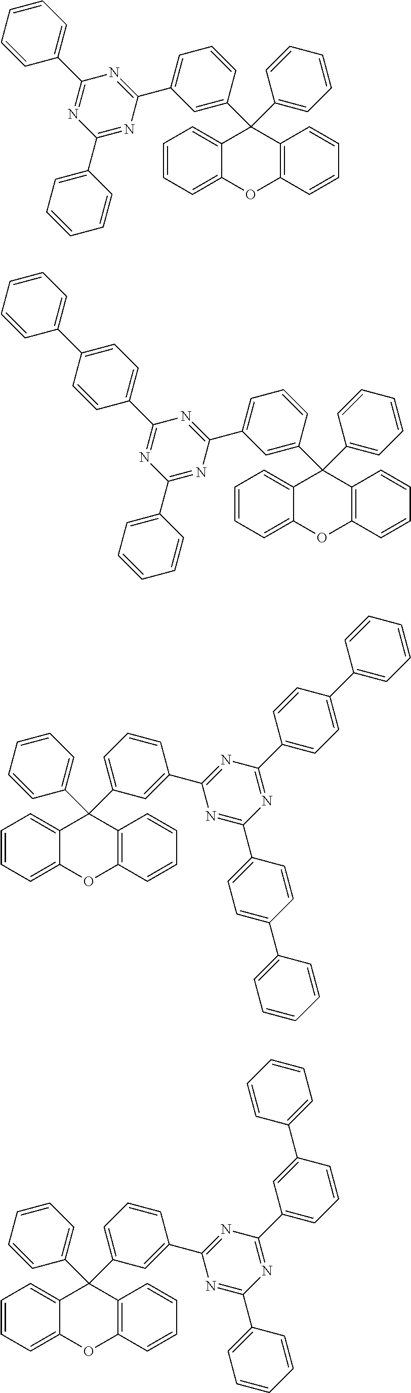
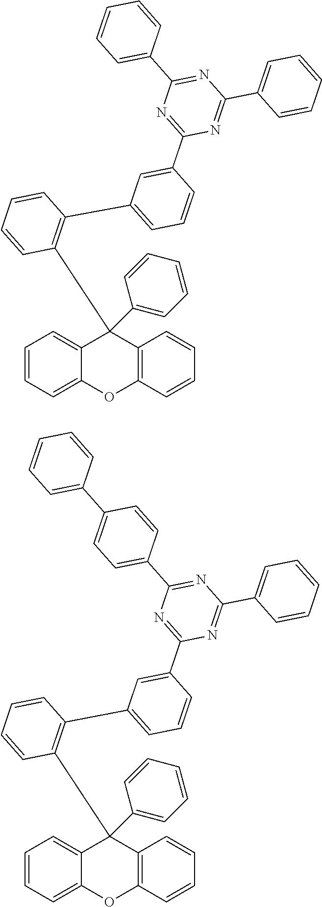
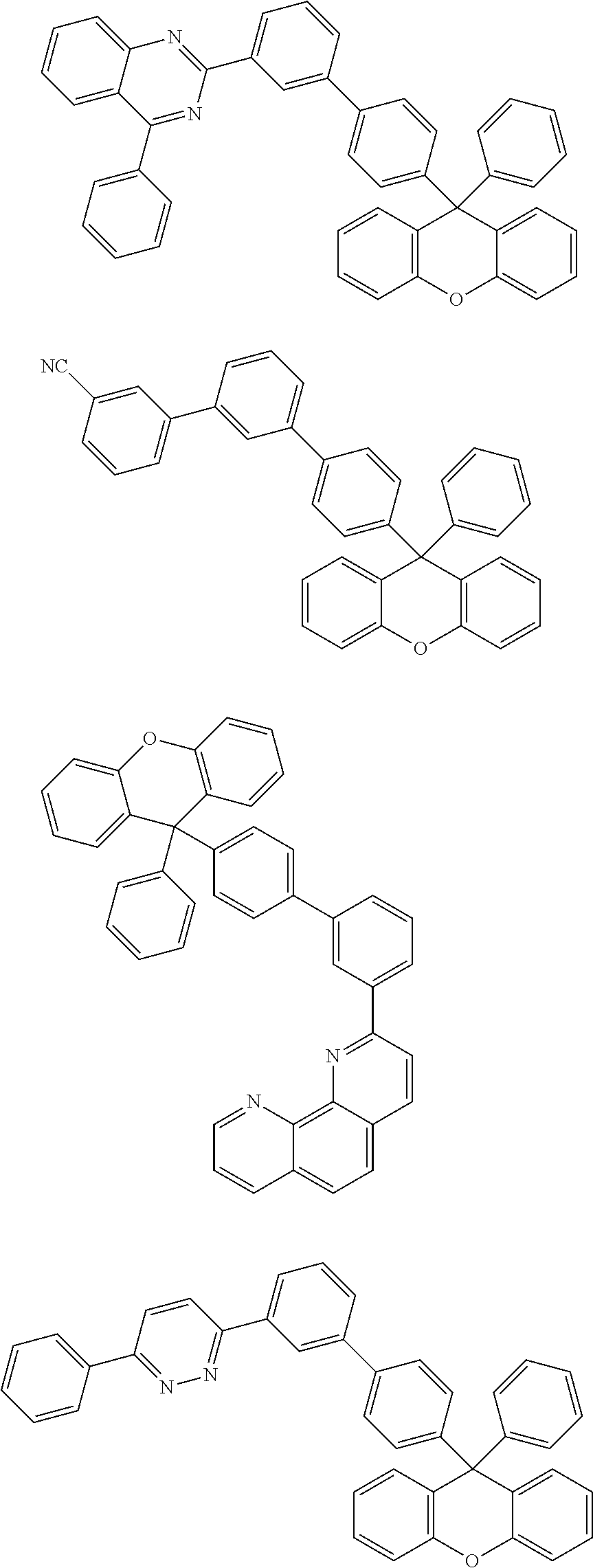
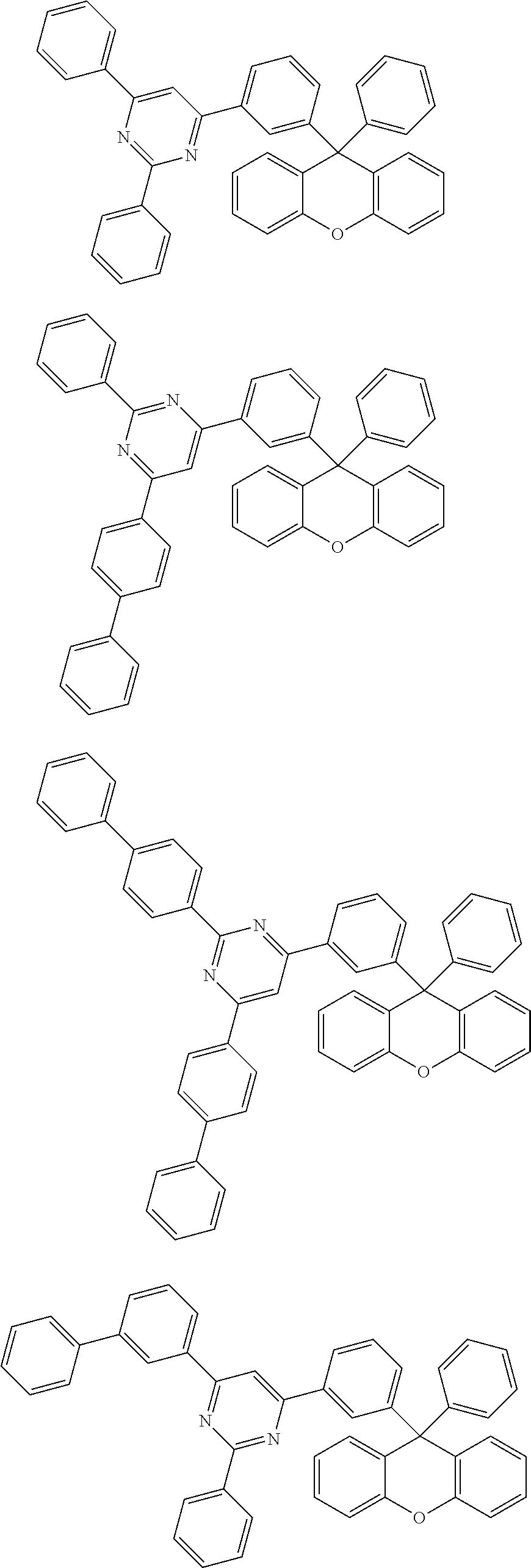
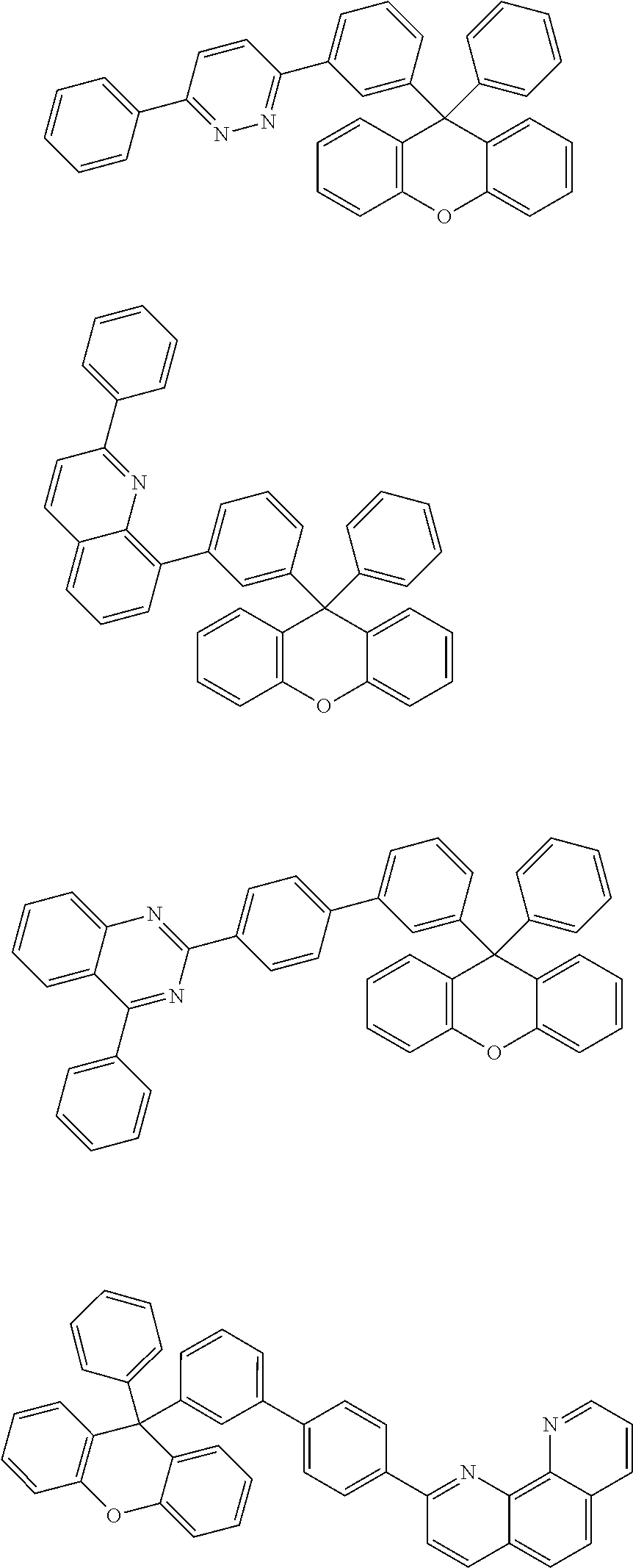
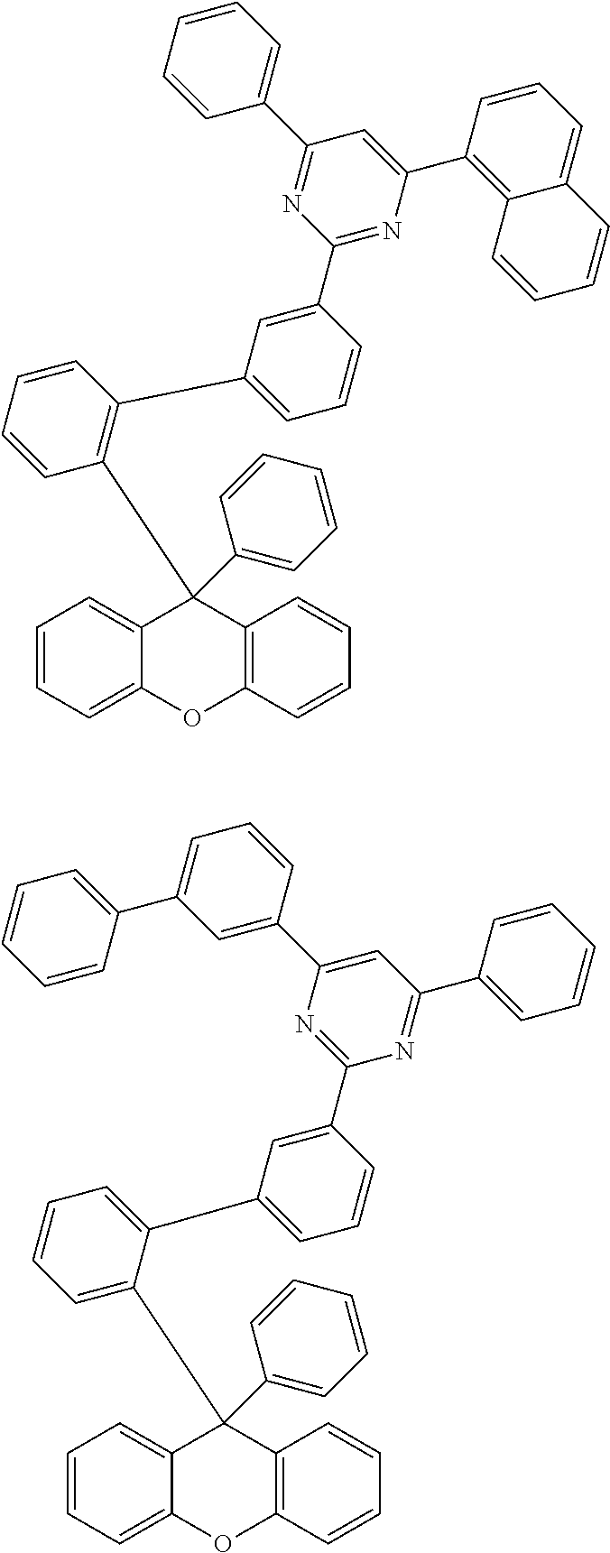
- the compound represented by Chemical Formula 1 is any one selected from the following structural formulae.
- the compound according to an exemplary embodiment of the present application may be prepared by a preparation method to be described below.
- a core structure of the compound of Chemical Formula 1 may be prepared as in the following Reaction Formula 1.
- the substituent may be bonded by a method known in the art, and the kind and position of the substituent or the number of substituents may be changed according to the technology known in the art.
- the bonding position of Br may be adjusted by using (3-bromophenyl) (phenyl)methanone or (2-bromophenyl) (phenyl)methanone instead of 2 A, and the compound of Chemical Formula 1 may be prepared by substituting Br with a substituent corresponding to the definition of Ar in Chemical Formula 1.
- the HOMO energy level of the compound represented by Chemical Formula 1 according to an exemplary embodiment of the present specification is 6.0 eV or more.
- the LUMO energy level of the compound represented by Chemical Formula 1 according to an exemplary embodiment of the present specification is 2.9 eV or more.
- the present specification provides an organic light emitting device including the above-described compound.
- An exemplary embodiment of the present application provides an organic light emitting device including: a first electrode; a second electrode disposed to face the first electrode; and an organic material layer having one or more layers disposed between the first electrode and the second electrode, in which one or more layers of the organic material layer include the compound.
- the organic material layer of the organic light emitting device of the present application may also be composed of a single-layered structure, but may be composed of a multi-layered structure in which two or more organic material layers are stacked.
- an organic light emitting device may have a structure including a hole injection layer, a hole transporting layer, a light emitting layer, an electron transporting layer, an electron injection layer, and the like as organic material layers.
- the structure of the organic light emitting device is not limited thereto, and may include a fewer number of organic material layers.
- the organic material layer includes a light emitting layer, and the light emitting layer includes the compound.
- the organic material layer includes a hole injection layer or a hole transporting layer, and the hole injection layer or the hole transporting layer includes the compound.
- the organic material layer includes an electron transporting layer or an electron injection layer, and the electron transporting layer or the electron injection layer includes the compound.
- the organic material layer includes an electron transporting layer, an electron injection layer, or an electron injection and transporting layer, and the electron transporting layer, the electron injection layer, or the electron injection or transporting layer includes the compound.
- the electron injection layer, the electron transporting layer, or the electron injection and transporting layer may include an additional compound.
- the electron injection layer, the electron transporting layer, or the electron injection and transporting layer may further include an N-type dopant.
- the electron injection layer, the electron transporting layer, or the electron injection and transporting layer may further include a metal complex.
- the electron injection layer, the electron transporting layer, or the electron injection and transporting layer may further include an alkali metal complex.
- the electron injection layer, the electron transporting layer, or the electron injection and transporting layer may further include lithium quinolate.
- the electron injection layer, the electron transporting layer, or the electron injection and transporting layer may include the compound of the present application and lithium quinolate at a weight ratio of 1:9 to 9:1.
- the electron injection layer, the electron transporting layer, or the electron injection and transporting layer may include the compound of the present application and lithium quinolate at a weight ratio of 4:6 to 6:4.
- the electron injection layer, the electron transporting layer, or the electron injection and transporting layer may include the compound of the present application and lithium quinolate at a weight ratio of 1:1.
- the organic material layer includes an electron blocking layer or a hole blocking layer, and the electron blocking layer or the hole blocking layer includes the compound.
- the organic material layer including the compound of Chemical Formula 1 has a thickness of 1 ⁇ to 1,000 ⁇ , and more preferably 1 ⁇ to 500 ⁇ .
- the organic light emitting device includes: a first electrode; a second electrode disposed to face the first electrode; a light emitting layer disposed between the first electrode and the second electrode; and an organic material layer having two or more layers disposed between the light emitting layer and the first electrode, or between the light emitting layer and the second electrode, in which at least one of the organic material layer having two or more layers includes the compound.
- two or more may be selected from the group consisting of an electron transporting layer, an electron injection layer, a layer which transports and injects electrons simultaneously, and a hole blocking layer.
- the organic material layer includes two or more electron transporting layers, and at least one of the two or more electron transporting layers includes the compound.
- the compound may also be included in one layer of the two or more electron transporting layers, and may be included in each layer of the two or more electron transporting layers.
- the other materials except for the compound may be the same as or different from each other.
- the organic material layer further includes a hole injection layer or a hole transporting layer, which includes a compound including an arylamino group, a carbazolyl group, or a benzocarbazolyl group, in addition to the organic material layer including the compound.
- a hole injection layer or a hole transporting layer which includes a compound including an arylamino group, a carbazolyl group, or a benzocarbazolyl group, in addition to the organic material layer including the compound.
- the organic light emitting device may be an organic light emitting device having a normal type structure in which a positive electrode, an organic material layer having one or more layers, and a negative electrode are sequentially stacked on a substrate.
- the organic light emitting device may be an organic light emitting device having an inverted type structure in which a negative electrode, an organic material layer having one or more layers, and a positive electrode are sequentially stacked on a substrate.
- FIGS. 1 and 2 the structure of the organic light emitting device according to an exemplary embodiment of the present application is exemplified in FIGS. 1 and 2 .
- FIG. 1 exemplifies a structure of an organic light emitting device in which a substrate 1 , a positive electrode 2 , a light emitting layer 3 , and a negative electrode 4 are sequentially stacked.
- the compound may be included in the light emitting layer 3 .
- FIG. 2 exemplifies a structure of an organic light emitting device in which a substrate 1 , a positive electrode 2 , a hole injection layer 5 , a hole transporting layer 6 , a light emitting layer 3 , an electron transporting layer 7 , and a negative electrode 4 are sequentially stacked.
- the compound may be included in one or more layers of the hole injection layer 5 , the hole transporting layer 6 , the light emitting layer 3 , and the electron transporting layer 7 .
- the compound may be included in one or more layers of the hole injection layer, the hole transporting layer, the light emitting layer, and the electron transporting layer.
- the organic light emitting device of the present application may be manufactured by the materials and methods known in the art, except that one or more layers of the organic material layer include the compound of the present application, that is, the compound.
- the organic material layers may be formed of the same material or different materials.
- the organic light emitting device of the present application may be manufactured by the materials and methods known in the art, except that one or more layers of the organic material layer include the compound, that is, the compound represented by Chemical Formula 1.
- the organic light emitting device of the present application may be manufactured by sequentially stacking a first electrode, an organic material layer, and a second electrode on a substrate.
- the organic light emitting device may be manufactured by depositing a metal or a metal oxide having conductivity, or an alloy thereof on a substrate to form a positive electrode, forming an organic material layer including a hole injection layer, a hole transporting layer, a light emitting layer, and an electron transporting layer thereon, and then depositing a material, which may be used as a negative electrode, thereon, by using a physical vapor deposition (PVD) method such as sputtering or e-beam evaporation.
- PVD physical vapor deposition
- an organic light emitting device may be made by sequentially depositing a negative electrode material, an organic material layer, and a positive electrode material on a substrate.
- the compound of Chemical Formula 1 may be formed as an organic material layer by not only a vacuum deposition method, but also a solution application method when an organic light emitting device is manufactured.
- the solution application method means spin coating, dip coating, doctor blading, inkjet printing, screen printing, a spray method, roll coating, and the like, but is not limited thereto.
- an organic light emitting device may also be made by sequentially depositing a negative electrode material, an organic material layer, and a positive electrode material on a substrate (International Publication No. 2003/012890).
- the manufacturing method is not limited thereto.
- the first electrode is a positive electrode
- the second electrode is a negative electrode
- the first electrode is a negative electrode
- the second electrode is a positive electrode
- the positive electrode material materials having a high work function are usually preferred so as to facilitate the injection of holes into an organic material layer.
- the positive electrode material which may be used in the present invention include: a metal such as vanadium, chromium, copper, zinc, and gold, or an alloy thereof; a metal oxide such as zinc oxide, indium oxide, indium tin oxide (ITO), and indium zinc oxide (IZO); a combination of a metal and an oxide, such as ZnO:Al or SnO 2 :Sb; a conductive polymer such as poly(3-methylthiophene), poly[3,4-(ethylene-1,2-dioxy)thiophene] (PEDOT), polypyrrole, and polyaniline; and the like, but are not limited thereto.
- a metal such as vanadium, chromium, copper, zinc, and gold, or an alloy thereof
- a metal oxide such as zinc oxide, indium oxide, indium tin oxide (ITO), and indium zinc oxide (IZO)
- the negative electrode material materials having a low work function are usually preferred so as to facilitate the injection of electrons into an organic material layer.
- the negative electrode material include: a metal such as magnesium, calcium, sodium, potassium, titanium, indium, yttrium, lithium, gadolinium, aluminum, silver, tin, and lead, or an alloy thereof; a multi-layer structured material, such as LiF/Al or LiO 2 /Al; and the like, but are not limited thereto.
- the hole injection layer is a layer which injects holes from an electrode
- a hole injection material is preferably a compound which has a capability of transporting holes and thus has an effect of injecting holes at a positive electrode and an excellent effect of injecting holes for a light emitting layer or a light emitting material, prevents excitons produced from the light emitting layer from moving to an electron injection layer or an electron injection material, and is also excellent in the ability to form a thin film.
- the highest occupied molecular orbital (HOMO) of the hole injection material is preferably a value between the work function of the positive electrode material and the HOMO of the neighboring organic material layer.
- the hole injection material examples include metal porphyrin, oligothiophene, arylamine-based organic materials, hexanitrile hexaazatriphenylene-based organic materials, quinacridone-based organic materials, perylene-based organic materials, anthraquinone, polyaniline-based and polythiophene-based conductive polymers, and the like, but are not limited thereto.
- the hole transporting layer is a layer which accepts holes from a hole injection layer and transports the holes to a light emitting layer
- a hole transporting material is suitably a material having high hole mobility which may accept holes from a positive electrode or a hole injection layer and transfer the holes to a light emitting layer.
- Specific examples thereof include arylamine-based organic materials, conductive polymers, block copolymers having both conjugated portions and non-conjugated portions, and the like, but are not limited thereto.
- the light emitting material is a material which may emit light in a visible light region by accepting and combining holes and electrons from a hole transporting layer and an electron transporting layer, respectively, and preferably a material having high quantum efficiency for fluorescence or phosphorescence.
- Specific examples thereof include: an 8-hydroxy-quinoline aluminum complex (Alq 3 ); carbazole-based compounds; dimerized styryl compounds; BAlq; 10-hydroxybenzoquinoline-metal compounds; benzoxazole-based, benzothiazole-based and benzimidazole-based compounds; poly(p-phenylenevinylene) (PPV)-based polymers; spiro compounds; polyfluorene, lubrene, and the like, but are not limited thereto.
- Alq 3 8-hydroxy-quinoline aluminum complex
- carbazole-based compounds dimerized styryl compounds
- BAlq 10-hydroxybenzoquinoline-metal compounds
- the light emitting layer may include a host material and a dopant material.
- the host material include a fused aromatic ring derivative, or a hetero ring-containing compound, and the like.
- the fused aromatic ring derivative include an anthracene derivative, a pyrene derivative, a naphthalene derivative, a pentacene derivative, a phenanthrene compound, a fluoranthene compound, and the like
- specific examples of the hetero ring-containing compound include a compound, a dibenzofuran derivative, a ladder-type furan compound, a pyrimidine derivative, and the like, but the examples are not limited thereto.
- the electron transporting layer is a layer which receives electrons from an electron injection layer and transports the electrons to a light emitting layer
- an electron transporting material is suitably a material having high electron mobility which may proficiently accept electrons from a negative electrode and transfer the electrons to a light emitting layer.
- Specific examples thereof include: an Al complex of 8-hydroxyquinoline; a complex including Alq 3 ; an organic radical compound; a hydroxyflavone-metal complex, and the like, but are not limited thereto.
- the electron transporting layer may be used with any desired cathode material, as used according to the related art.
- appropriate examples of the cathode material are a typical material which has a low work function, followed by an aluminum layer or a silver layer.
- Specific examples thereof include cesium, barium, calcium, ytterbium, and samarium, in each case followed by an aluminum layer or a silver layer.
- the electron injection layer is a layer which injects electrons from an electrode
- an electron injection material is preferably a compound which has a capability of transporting electrons, an effect of injecting electrons from a negative electrode, and an excellent effect of injecting electrons into a light emitting layer or a light emitting material, prevents excitons produced from the light emitting layer from moving to a hole injection layer, and is also excellent in the ability to form a thin film.
- fluorenone anthraquinodimethane, diphenoquinone, thiopyran dioxide, oxazole, oxadiazole, triazole, imidazole, perylenetetracarboxylic acid, fluorenylidene methane, anthrone, and the like, and a derivative thereof, a metal complex compound, a nitrogen-containing 5-membered ring derivative, and the like, but are not limited thereto.
- Examples of the metal complex compound include 8-hydroxyquinolinato lithium, bis(8-hydroxyquinolinato) zinc, bis(8-hydroxyquinolinato) copper, bis(8-hydroxyquinolinato) manganese, tris(8-hydroxyquinolinato) aluminum, tris(2-methyl-8-hydroxyquinolinato) aluminum, tris(8-hydroxyquinolinato) gallium, bis(10-hydroxybenzo[h]quinolinato) beryllium, bis(10-hydroxybenzo[h]quinolinato) zinc, bis(2-methyl-8-quinolinato) chlorogallium, bis(2-methyl-8-quinolinato) (o-cresolato) gallium, bis(2-methyl-8-quinolinato) (1-naphtholato) aluminum, bis(2-methyl-8-quinolinato) (2-naphtholato) gallium, and the like, but are not limited thereto.
- the hole blocking layer is a layer which blocks holes from reaching a negative electrode, and may be generally formed under the same conditions as those of the hole injection layer. Specific examples thereof include an oxadiazole derivative or a triazole derivative, a phenanthroline derivative, BCP, an aluminum complex, and the like, but are not limited thereto.
- the organic light emitting device may be a top emission type, a bottom emission type, or a dual emission type according to the materials to be used.
- a glass substrate thinly coated with indium tin oxide (ITO) to have a thickness of 1,000 ⁇ was put into distilled water in which a detergent was dissolved, and ultrasonically washed.
- ITO indium tin oxide
- a product manufactured by Fischer Co. was used as the detergent
- distilled water twice filtered using a filter manufactured by Millipore Co. was used as the distilled water.
- ultrasonic washing was repeated twice by using distilled water for 10 minutes.
- ultrasonic washing was conducted by using a solvent of isopropyl alcohol, acetone, and methanol, and the resultant product was dried and then transported to a plasma washing machine.
- the substrate was washed by using an oxygen plasma for 5 minutes, and then was transported to a vacuum deposition machine.
- HAT Hexanitrile hexaazatriphenylene
- the compound of [Chemical Formula E1] and the following compound [LiQ] (lithium quinolate) were vacuum deposited at a weight ratio of 1:1 on the light emitting layer, thereby forming an electron injection and transporting layer having a thickness of 350 ⁇ .
- Lithium fluoride (LiF) and aluminum were sequentially deposited to have a thickness of 10 ⁇ and 1,000 ⁇ , respectively, on the electron injection and transporting layer, thereby forming a negative electrode.
- the deposition rate of the organic material was maintained at 0.4 to 0.9 ⁇ /sec
- the deposition rates of lithium fluoride and aluminum of the negative electrode were maintained at 0.3 ⁇ /sec and at 2 ⁇ /sec, respectively
- the degree of vacuum during the deposition was maintained at 1 ⁇ 10 ⁇ 7 to 5 ⁇ 10 ⁇ 8 torr, thereby manufacturing an organic light emitting device.
- An organic light emitting device was manufactured in the same manner as in Experimental Example 1-1, except that the compound of Chemical Formula E2 was used instead of the compound of Chemical Formula E1 in Experimental Example 1-1.
- An organic light emitting device was manufactured in the same manner as in Experimental Example 1-1, except that the compound of Chemical Formula E3 was used instead of the compound of Chemical Formula E1 in Experimental Example 1-1.
- An organic light emitting device was manufactured in the same manner as in Experimental Example 1-1, except that the compound of Chemical Formula E4 was used instead of the compound of Chemical Formula E1 in Experimental Example 1-1.
- An organic light emitting device was manufactured in the same manner as in Experimental Example 1-1, except that the compound of Chemical Formula E5 was used instead of the compound of Chemical Formula E1 in Experimental Example 1-1.
- An organic light emitting device was manufactured in the same manner as in Experimental Example 1-1, except that the compound of Chemical Formula E6 was used instead of the compound of Chemical Formula E1 in Experimental Example 1-1.
- An organic light emitting device was manufactured in the same manner as in Experimental Example 1-1, except that the compound of Chemical Formula E7 was used instead of the compound of Chemical Formula E1 in Experimental Example 1-1.
- An organic light emitting device was manufactured in the same manner as in Experimental Example 1-1, except that the compound of Chemical Formula E8 was used instead of the compound of Chemical Formula E1 in Experimental Example 1-1.
- An organic light emitting device was manufactured in the same manner as in Experimental Example 1-1, except that the compound of Chemical Formula E9 was used instead of the compound of Chemical Formula E1 in Experimental Example 1-1.
- An organic light emitting device was manufactured in the same manner as in Experimental Example 1-1, except that the compound of Chemical Formula E10 was used instead of the compound of Chemical Formula E1 in Experimental Example 1-1.
- An organic light emitting device was manufactured in the same manner as in Experimental Example 1-1, except that the compound of Chemical Formula E12 was used instead of the compound of Chemical Formula E1 in Experimental Example 1-1.
- An organic light emitting device was manufactured in the same manner as in Experimental Example 1-1, except that the compound of Chemical Formula E13 was used instead of the compound of Chemical Formula E1 in Experimental Example 1-1.
- An organic light emitting device was manufactured in the same manner as in Experimental Example 1-1, except that the compound of Chemical Formula E14 was used instead of the compound of Chemical Formula E1 in Experimental Example 1-1.
- An organic light emitting device was manufactured in the same manner as in Experimental Example 1-1, except that the compound of Chemical Formula ET-1-A was used instead of the compound of Chemical Formula E1 in Experimental Example 1-1.
- An organic light emitting device was manufactured in the same manner as in Experimental Example 1-1, except that the compound of Chemical Formula ET-1-B was used instead of the compound of Chemical Formula E1 in Experimental Example 1-1.
- An organic light emitting device was manufactured in the same manner as in Experimental Example 1-1, except that the compound of Chemical Formula ET-1-C was used instead of the compound of Chemical Formula E1 in Experimental Example 1-1.
- An organic light emitting device was manufactured in the same manner as in Experimental Example 1-1, except that the compound of Chemical Formula ET-1-D was used instead of the compound of Chemical Formula E1 in Experimental Example 1-1.
- An organic light emitting device was manufactured in the same manner as in Experimental Example 1-1, except that the compound of Chemical Formula ET-1-E was used instead of the compound of Chemical Formula E1 in Experimental Example 1-1.
- An organic light emitting device was manufactured in the same manner as in Experimental Example 1-1, except that the compound of Chemical Formula ET-1-F was used instead of the compound of Chemical Formula E1 in Experimental Example 1-1.
- An organic light emitting device was manufactured in the same manner as in Experimental Example 1-1, except that the compound of Chemical Formula ET-1-G was used instead of the compound of Chemical Formula E1 in Experimental Example 1-1.
- An organic light emitting device was manufactured in the same manner as in Experimental Example 1-1, except that the compound of Chemical Formula ET-1-H was used instead of the compound of Chemical Formula E1 in Experimental Example 1-1.
- An organic light emitting device was manufactured in the same manner as in Experimental Example 1-1, except that the compound of Chemical Formula ET-1-I was used instead of the compound of Chemical Formula E1 in Experimental Example 1-1.
- An organic light emitting device was manufactured in the same manner as in Experimental Example 1-1, except that the compound of Chemical Formula ET-1-J was used instead of the compound of Chemical Formula E1 in Experimental Example 1-1.
- FIG. 5 the HOMO energy level of Compound [ET-1-J], which was measured by using a photoelectron spectrometer, is illustrated in FIG. 5
- FIG. 8 the absorption and emission spectra of Compound [ET-1-J], which were measured by using photoluminescence, are illustrated in FIG. 8 .
- An organic light emitting device was manufactured in the same manner as in Experimental Example 1-1, except that the compound of Chemical Formula ET-1-K was used instead of the compound of Chemical Formula E1 in Experimental Example 1-1.
- An organic light emitting device was manufactured in the same manner as in Experimental Example 1-1, except that the compound of Chemical Formula ET-1-L was used instead of the compound of Chemical Formula E1 in Experimental Example 1-1.
- heterocyclic compound represented by Chemical Formula 1 may be used for an organic material layer of an organic light emitting device which may simultaneously inject and transport electrons.
- the compound represented by Chemical Formula 1 according to an exemplary embodiment of the present specification has excellent thermal stability, a deep HOMO level of 6.0 eV or more, a high triplet energy (ET), and hole stability and thus may exhibit excellent characteristics.
- the compound represented by Chemical Formula 1 when used in the organic material layer which may simultaneously inject and transport electrons, the compound may be used in a mixture with an n-type dopant used in the art.
- the compound represented by Chemical Formula 1 may have low driving voltage and high efficiency, and may improve stability of the device by hole stability of the compound.
- the HOMO level was measured by using an atmospheric pressure photoelectron spectrometer (AC3: manufactured by RIKEN KEIKI Co., Ltd.).
- the LUMO level was calculated as a wavelength value measured via photoluminescence (PL).
Landscapes
- Chemical & Material Sciences (AREA)
- Organic Chemistry (AREA)
- Physics & Mathematics (AREA)
- Spectroscopy & Molecular Physics (AREA)
- Engineering & Computer Science (AREA)
- Materials Engineering (AREA)
- Optics & Photonics (AREA)
- Electroluminescent Light Sources (AREA)
- Nitrogen Condensed Heterocyclic Rings (AREA)
- Pyrane Compounds (AREA)
- Plural Heterocyclic Compounds (AREA)
- Organic Low-Molecular-Weight Compounds And Preparation Thereof (AREA)
Abstract
Description


-
- 1: Substrate
- 2: Positive electrode
- 3: Light emitting layer
- 4: Negative electrode
- 5: Hole injection layer
- 6: Hole transporting layer
- 7: Electron transporting layer
and a dotted line mean a site bonded to another substituent or a binding portion.

and the like, but is not limited thereto.
a pyridazinyl group, a pyrazinyl group, a quinolinyl group, a quinazolinyl group, a quinoxalinyl group, a phthalazinyl group, a pyridopyrimidinyl group, a pyridopyrazinyl group, a pyrazinopyrazinyl group, an isoquinolinyl group, an indole group, a carbazolyl group, a benzoxazolyl group, a benzimidazolyl group, a benzothiazolyl group, a benzocarbazolyl group, a dibenzocarbazolyl group, a benzothiophenyl group, a dibenzothiophenyl group, a benzofuranyl group, a dibenzofuranyl group; a benzosilole group; a dibenzosilole group; a phenanthrolinyl group, a thiazolyl group, an isoxazolyl group, an oxadiazolyl group, a thiadiazolyl group, a benzothiazolyl group, a phenothiazinyl group, a phenoxazinyl group, and fused structures thereof, and the like, but are not limited thereto. In addition, examples of the heterocyclic group include a heterocyclic structure including a sulfonyl group, for example,

and the like.


MS[M+H]+=642

MS[M+H]+=642

MS[M+H]+=641

MS[M+H]+=642

MS[M+H]+=539

MS[M+H]+=589

MS[M+H]+=589

MS[M+H]+=656

MS[M+H]+=642

MS[M+H]+=489

MS[M+H]+=718

MS[M+H]+=512

MS[M+H]+=616

MS[M+H]+=742

MS[M+H]+=717


| TABLE 1 | |||||
| Service | |||||
| Voltage | Efficiency | Color | life (h) | ||
| Chemical | (V@10 | (cd/A@10 | coordinate | T90 at 20 | |
| Formula | mA/cm2) | mA/cm2) | (x, y) | mA/cm2 | |
| Experimental | E1 | 4.37 | 5.77 | (0.142, | 110 |
| Example 1-1 | 0.097) | ||||
| Experimental | E2 | 4.25 | 5.80 | (0.142, | 100 |
| Example 1-2 | 0.096) | ||||
| Experimental | E3 | 4.44 | 5.82 | (0.142, | 98 |
| Example 1-3 | 0.096) | ||||
| Experimental | E4 | 4.30 | 5.75 | (0.142, | 106 |
| Example 1-4 | 0.096) | ||||
| Experimental | E5 | 4.50 | 5.34 | (0.142, | 97 |
| Example 1-5 | 0.096) | ||||
| Experimental | E6 | 4.41 | 5.40 | (0.142, | 115 |
| Example 1-6 | 0.097) | ||||
| Experimental | E7 | 4.47 | 5.39 | (0.142, | 112 |
| Example 1-7 | 0.096) | ||||
| Experimental | E8 | 4.39 | 5.71 | (0.142, | 129 |
| Example 1-8 | 0.099) | ||||
| Experimental | E9 | 4.48 | 5.30 | (0.142, | 96 |
| Example 1-9 | 0.096) | ||||
| Experimental | E10 | 4.39 | 5.68 | (0.142, | 133 |
| Example 1-10 | 0.098) | ||||
| Experimental | E11 | 4.31 | 5.70 | (0.142, | 136 |
| Example 1-11 | 0.096) | ||||
| Experimental | E12 | 4.47 | 5.48 | (0.142, | 160 |
| Example 1-12 | 0.097) | ||||
| Experimental | E13 | 4.21 | 5.75 | (0.142, | 120 |
| Example 1-13 | 0.096) | ||||
| Experimental | E14 | 4.33 | 5.80 | (0.142, | 100 |
| Example 1-14 | 0.097) | ||||
| Experimental | E15 | 4.30 | 5.84 | (0.142, | 101 |
| Example 1-15 | 0.097) | ||||
| Comparative | ET-1-A | 4.50 | 4.70 | (0.142, | 90 |
| Example 1-1 | 0.098) | ||||
| Comparative | ET-1-B | 4.84 | 4.01 | (0.142, | 77 |
| Example 1-2 | 0.102) | ||||
| Comparative | ET-1-C | 4.99 | 2.99 | (0.142, | 81 |
| Example 1-3 | 0.096) | ||||
| Comparative | ET-1-D | 4.70 | 4.00 | (0.142, | 57 |
| Example 1-4 | 0.096) | ||||
| Comparative | ET-1-E | 5.11 | 3.50 | (0.142, | 65 |
| Example 1-5 | 0.096) | ||||
| Comparative | ET-1-F | 4.33 | 5.00 | (0.142, | 30 |
| Example 1-6 | 0.096) | ||||
| Comparative | ET-1-G | 5.33 | 3.21 | (0.142, | 40 |
| Example 1-7 | 0.096) | ||||
| Comparative | ET-1-H | 5.45 | 3.18 | (0.142, | 45 |
| Example 1-8 | 0.096) | ||||
| Comparative | ET-1-I | 5.59 | 3.07 | (0.142, | 52 |
| Example 1-9 | 0.096) | ||||
| Comparative | ET-1-J | 5.00 | 3.77 | (0.142, | 80 |
| Example 1-10 | 0.096) | ||||
| Comparative | ET-1-K | 4.55 | 4.51 | (0.142, | 88 |
| Example 1-11 | 0.097) | ||||
| Comparative | ET-1-L | 4.40 | 5.05 | (0.142, | 27 |
| Example 1-12 | 0.097) | ||||

| TABLE 2 | ||
| Chemical Formula | HOMO (eV) | LUMO (eV) |
| E1 | 6.22 | 2.96 |
| E3 | 6.18 | 2.93 |
| ET-1-J | 5.70 | 2.87 |
Claims (7)


Applications Claiming Priority (3)
| Application Number | Priority Date | Filing Date | Title |
|---|---|---|---|
| KR20160101362 | 2016-08-09 | ||
| KR10-2016-0101362 | 2016-08-09 | ||
| PCT/KR2017/008621 WO2018030786A1 (en) | 2016-08-09 | 2017-08-09 | Compound and organic light-emitting device comprising same |
Publications (2)
| Publication Number | Publication Date |
|---|---|
| US20190189929A1 US20190189929A1 (en) | 2019-06-20 |
| US11653564B2 true US11653564B2 (en) | 2023-05-16 |
Family
ID=61163036
Family Applications (1)
| Application Number | Title | Priority Date | Filing Date |
|---|---|---|---|
| US16/322,065 Active 2038-12-02 US11653564B2 (en) | 2016-08-09 | 2017-08-09 | Compound and organic light-emitting device comprising same |
Country Status (7)
| Country | Link |
|---|---|
| US (1) | US11653564B2 (en) |
| EP (1) | EP3483152B1 (en) |
| JP (1) | JP6760582B2 (en) |
| KR (1) | KR101922649B1 (en) |
| CN (1) | CN109563065B (en) |
| TW (1) | TWI653231B (en) |
| WO (1) | WO2018030786A1 (en) |
Families Citing this family (7)
| Publication number | Priority date | Publication date | Assignee | Title |
|---|---|---|---|---|
| KR102233985B1 (en) * | 2018-08-10 | 2021-03-30 | 주식회사 엘지화학 | Novel compound and organic light emitting device comprising the same |
| KR102168068B1 (en) | 2018-08-17 | 2020-10-20 | 주식회사 엘지화학 | Novel compound and organic light emitting device comprising the same |
| CN112513035B (en) * | 2018-10-04 | 2024-08-02 | 株式会社Lg化学 | Compound and organic light emitting diode comprising the same |
| CN112409243A (en) * | 2019-08-23 | 2021-02-26 | 支志明 | Tetradentate ligand, gold (III) complex, and preparation method and application thereof |
| KR102807677B1 (en) * | 2020-04-17 | 2025-05-20 | 덕산네오룩스 주식회사 | Compound for organic electronic element, organic electronic element using the same, and an electronic device thereof |
| KR102573735B1 (en) | 2020-07-13 | 2023-08-31 | 주식회사 엘지화학 | Novel compound and organic light emitting device comprising the same |
| CN116349430A (en) * | 2021-09-01 | 2023-06-27 | 株式会社Lg化学 | Compound and organic light-emitting device containing same |
Citations (14)
| Publication number | Priority date | Publication date | Assignee | Title |
|---|---|---|---|---|
| KR20110102371A (en) | 2008-11-26 | 2011-09-16 | 코닌클리즈케 필립스 일렉트로닉스 엔.브이. | OLD with novel hole-conductive material |
| US20110240983A1 (en) * | 2008-12-12 | 2011-10-06 | Canon Kabushiki Kaisha | Triazine compound and organic light emitting device using the same |
| US20120228554A1 (en) | 2009-11-17 | 2012-09-13 | Merck Patent Gmbh | Materials for organic electroluminescent devices |
| KR20140108778A (en) | 2013-02-28 | 2014-09-15 | 에스에프씨 주식회사 | An electroluminescent compound and an electroluminescent device comprising the same |
| KR20140135117A (en) | 2013-05-15 | 2014-11-25 | 에스에프씨 주식회사 | An electroluminescent compound and an electroluminescent device comprising the same |
| KR20150002740A (en) | 2012-04-02 | 2015-01-07 | 노발레드 게엠베하 | Use of a semiconducting compound in an organic light emitting device |
| KR20150077263A (en) | 2013-12-27 | 2015-07-07 | 주식회사 두산 | Organic lighting-emitting compound and organic electroluminescent device using the same |
| KR20150083917A (en) | 2012-11-12 | 2015-07-20 | 메르크 파텐트 게엠베하 | Materials for electronic devices |
| KR20160018406A (en) | 2014-08-08 | 2016-02-17 | 롬엔드하스전자재료코리아유한회사 | Organic electroluminescent compounds and organic electroluminescent devices comprising the same |
| US20160118599A1 (en) | 2014-10-22 | 2016-04-28 | Samsung Display Co., Ltd. | Compound and organic light-emitting device including the same |
| WO2016096851A1 (en) | 2014-12-15 | 2016-06-23 | Cynora Gmbh | Ambipolar host materials for optoelectronic components |
| CN106478611A (en) | 2016-08-26 | 2017-03-08 | 江苏三月光电科技有限公司 | A kind of organic compound with xanthene as core and its application |
| CN106478610A (en) | 2016-08-26 | 2017-03-08 | 江苏三月光电科技有限公司 | A kind of organic compound containing xanthene and its application in OLED |
| CN107056763A (en) | 2016-04-25 | 2017-08-18 | 中节能万润股份有限公司 | A kind of electroluminescent organic material and its application using xanthene as core |
Family Cites Families (3)
| Publication number | Priority date | Publication date | Assignee | Title |
|---|---|---|---|---|
| DE10135513B4 (en) | 2001-07-20 | 2005-02-24 | Novaled Gmbh | Light-emitting component with organic layers |
| WO2014058123A1 (en) * | 2012-10-08 | 2014-04-17 | 제일모직 주식회사 | Compound for organic optoelectric device, organic light emitting diode comprising same, and display device comprising organic light emitting diode |
| KR20160101362A (en) | 2015-02-17 | 2016-08-25 | 전용남 | composition of rubber |
-
2017
- 2017-08-09 KR KR1020170101073A patent/KR101922649B1/en active Active
- 2017-08-09 EP EP17839804.6A patent/EP3483152B1/en active Active
- 2017-08-09 WO PCT/KR2017/008621 patent/WO2018030786A1/en not_active Ceased
- 2017-08-09 US US16/322,065 patent/US11653564B2/en active Active
- 2017-08-09 JP JP2019503314A patent/JP6760582B2/en active Active
- 2017-08-09 TW TW106126848A patent/TWI653231B/en active
- 2017-08-09 CN CN201780048270.1A patent/CN109563065B/en active Active
Patent Citations (22)
| Publication number | Priority date | Publication date | Assignee | Title |
|---|---|---|---|---|
| US20110227054A1 (en) | 2008-11-26 | 2011-09-22 | Koninklijke Philips Electronics N.V. | Oled including hole-conducting material |
| KR20110102371A (en) | 2008-11-26 | 2011-09-16 | 코닌클리즈케 필립스 일렉트로닉스 엔.브이. | OLD with novel hole-conductive material |
| US20110240983A1 (en) * | 2008-12-12 | 2011-10-06 | Canon Kabushiki Kaisha | Triazine compound and organic light emitting device using the same |
| US20120228554A1 (en) | 2009-11-17 | 2012-09-13 | Merck Patent Gmbh | Materials for organic electroluminescent devices |
| JP2013510889A (en) | 2009-11-17 | 2013-03-28 | メルク パテント ゲーエムベーハー | Materials for organic electroluminescent devices |
| US20160096809A1 (en) * | 2009-11-17 | 2016-04-07 | Merck Patent Gmbh | Materials for organic electroluminescent devices |
| KR20150002740A (en) | 2012-04-02 | 2015-01-07 | 노발레드 게엠베하 | Use of a semiconducting compound in an organic light emitting device |
| US20150115241A1 (en) | 2012-04-02 | 2015-04-30 | Novaled Gmbh | Use of a Semiconducting Compound in an Organic Light Emitting Device |
| KR20150083917A (en) | 2012-11-12 | 2015-07-20 | 메르크 파텐트 게엠베하 | Materials for electronic devices |
| US20150295181A1 (en) | 2012-11-12 | 2015-10-15 | Merck Patent Gmbh | Materials for electronic devices |
| KR20140108778A (en) | 2013-02-28 | 2014-09-15 | 에스에프씨 주식회사 | An electroluminescent compound and an electroluminescent device comprising the same |
| US20150333277A1 (en) | 2013-05-15 | 2015-11-19 | Sfc Co., Ltd. | Organic light emitting compound and organic light emitting device including the same |
| KR20140135117A (en) | 2013-05-15 | 2014-11-25 | 에스에프씨 주식회사 | An electroluminescent compound and an electroluminescent device comprising the same |
| KR20150077263A (en) | 2013-12-27 | 2015-07-07 | 주식회사 두산 | Organic lighting-emitting compound and organic electroluminescent device using the same |
| KR20160018406A (en) | 2014-08-08 | 2016-02-17 | 롬엔드하스전자재료코리아유한회사 | Organic electroluminescent compounds and organic electroluminescent devices comprising the same |
| US20170217992A1 (en) | 2014-08-08 | 2017-08-03 | Rohm And Haas Electronic Materials Korea Ltd. | Organic electroluminescent compounds and organic electroluminescent devices comprising the same |
| US20160118599A1 (en) | 2014-10-22 | 2016-04-28 | Samsung Display Co., Ltd. | Compound and organic light-emitting device including the same |
| KR20160047670A (en) | 2014-10-22 | 2016-05-03 | 삼성디스플레이 주식회사 | Compound and organic light emitting device comprising same |
| WO2016096851A1 (en) | 2014-12-15 | 2016-06-23 | Cynora Gmbh | Ambipolar host materials for optoelectronic components |
| CN107056763A (en) | 2016-04-25 | 2017-08-18 | 中节能万润股份有限公司 | A kind of electroluminescent organic material and its application using xanthene as core |
| CN106478611A (en) | 2016-08-26 | 2017-03-08 | 江苏三月光电科技有限公司 | A kind of organic compound with xanthene as core and its application |
| CN106478610A (en) | 2016-08-26 | 2017-03-08 | 江苏三月光电科技有限公司 | A kind of organic compound containing xanthene and its application in OLED |
Non-Patent Citations (2)
| Title |
|---|
| ‘Reactions of 9-Phenylxanthylium Salts with Organometallic Reagents. I’, Chemical and Pharmaceutical Bulletin, 1973, vol. 21, No. 6, p. 1318-1326. |
| Supplementary Search Report of European Patent Office in Appl'n No. EP17839804, dated May 20, 2019. |
Also Published As
| Publication number | Publication date |
|---|---|
| JP2019524751A (en) | 2019-09-05 |
| TWI653231B (en) | 2019-03-11 |
| EP3483152A4 (en) | 2019-06-19 |
| KR101922649B1 (en) | 2018-11-27 |
| CN109563065A (en) | 2019-04-02 |
| TW201811764A (en) | 2018-04-01 |
| EP3483152B1 (en) | 2021-04-28 |
| WO2018030786A1 (en) | 2018-02-15 |
| JP6760582B2 (en) | 2020-09-23 |
| US20190189929A1 (en) | 2019-06-20 |
| KR20180018400A (en) | 2018-02-21 |
| CN109563065B (en) | 2022-09-13 |
| EP3483152A1 (en) | 2019-05-15 |
Similar Documents
| Publication | Publication Date | Title |
|---|---|---|
| US11877510B2 (en) | Heterocyclic compound and organic light-emitting element comprising same | |
| US12415801B2 (en) | Organic light-emitting device | |
| US12098156B2 (en) | Compound and organic light emitting device comprising the same | |
| US11518769B2 (en) | Heterocyclic compounds and organic light emitting device using the same | |
| US11718606B2 (en) | Polycyclic compound and organic light emitting element comprising same | |
| US11997925B2 (en) | Cyclic compound and organic light emitting device comprising same | |
| US20200365814A1 (en) | Organic light-emitting device | |
| US11910711B2 (en) | Cyclic compound and organic light emitting device comprising same | |
| US20180337341A1 (en) | Heterocyclic compound and organic light emitting element comprising same | |
| US11653564B2 (en) | Compound and organic light-emitting device comprising same | |
| US12250879B2 (en) | Heterocyclic compound and organic light emitting device comprising the same | |
| US11569453B2 (en) | Polycyclic compound and organic light emitting element comprising same | |
| US11453650B2 (en) | Heterocyclic compound and organic light emitting device comprising the same | |
| US10738034B2 (en) | Spiro compound and organic light-emitting device comprising same | |
| US11367836B2 (en) | Heterocyclic compound and organic light emitting element including same | |
| US11968897B2 (en) | Heterocyclic compound and organic light emitting diode containing same | |
| US20210265572A1 (en) | Novel heterocyclic compound and organic light emitting device comprising the same | |
| US12133459B2 (en) | Heterocyclic compound and organic light emitting device comprising same | |
| US11856852B2 (en) | Organic light-emitting device | |
| US11795161B2 (en) | Compound and organic light emitting device comprising same | |
| US20240190850A1 (en) | Novel compound and organic light emitting device comprising the same | |
| US11261176B2 (en) | Amine-based compound and organic light emitting device using the same | |
| US11778909B2 (en) | Compound and organic light emitting device comprising the same | |
| US20240381763A1 (en) | Novel compound and organic light emitting device comprising the same | |
| US12202838B2 (en) | Heterocyclic compound and organic light emitting device comprising same |
Legal Events
| Date | Code | Title | Description |
|---|---|---|---|
| AS | Assignment |
Owner name: LG CHEM, LTD., KOREA, REPUBLIC OF Free format text: ASSIGNMENT OF ASSIGNORS INTEREST;ASSIGNORS:HEO, DONG UK;LEE, DONG HOON;HUH, JUNGOH;AND OTHERS;REEL/FRAME:048194/0874 Effective date: 20170906 |
|
| FEPP | Fee payment procedure |
Free format text: ENTITY STATUS SET TO UNDISCOUNTED (ORIGINAL EVENT CODE: BIG.); ENTITY STATUS OF PATENT OWNER: LARGE ENTITY |
|
| STPP | Information on status: patent application and granting procedure in general |
Free format text: DOCKETED NEW CASE - READY FOR EXAMINATION |
|
| STPP | Information on status: patent application and granting procedure in general |
Free format text: NON FINAL ACTION MAILED |
|
| STPP | Information on status: patent application and granting procedure in general |
Free format text: RESPONSE TO NON-FINAL OFFICE ACTION ENTERED AND FORWARDED TO EXAMINER |
|
| STPP | Information on status: patent application and granting procedure in general |
Free format text: FINAL REJECTION MAILED |
|
| STPP | Information on status: patent application and granting procedure in general |
Free format text: DOCKETED NEW CASE - READY FOR EXAMINATION |
|
| STPP | Information on status: patent application and granting procedure in general |
Free format text: NON FINAL ACTION MAILED |
|
| STPP | Information on status: patent application and granting procedure in general |
Free format text: RESPONSE TO NON-FINAL OFFICE ACTION ENTERED AND FORWARDED TO EXAMINER |
|
| STCF | Information on status: patent grant |
Free format text: PATENTED CASE |