US11653510B2 - Adhesive transparent electrode and method of fabricating the same - Google Patents
Adhesive transparent electrode and method of fabricating the same Download PDFInfo
- Publication number
- US11653510B2 US11653510B2 US16/169,174 US201816169174A US11653510B2 US 11653510 B2 US11653510 B2 US 11653510B2 US 201816169174 A US201816169174 A US 201816169174A US 11653510 B2 US11653510 B2 US 11653510B2
- Authority
- US
- United States
- Prior art keywords
- based polymer
- silicone
- adhesive
- pdms
- transparent electrode
- Prior art date
- Legal status (The legal status is an assumption and is not a legal conclusion. Google has not performed a legal analysis and makes no representation as to the accuracy of the status listed.)
- Active, expires
Links
- 239000000853 adhesive Substances 0.000 title claims abstract description 150
- 230000001070 adhesive effect Effects 0.000 title claims abstract description 150
- 238000004519 manufacturing process Methods 0.000 title claims abstract description 17
- 239000011159 matrix material Substances 0.000 claims abstract description 145
- 229920001296 polysiloxane Polymers 0.000 claims abstract description 90
- 229920000642 polymer Polymers 0.000 claims abstract description 86
- 239000002070 nanowire Substances 0.000 claims abstract description 54
- 239000000758 substrate Substances 0.000 claims abstract description 48
- 229910052751 metal Inorganic materials 0.000 claims abstract description 47
- 239000002184 metal Substances 0.000 claims abstract description 47
- 239000002736 nonionic surfactant Substances 0.000 claims abstract description 35
- 239000004971 Cross linker Substances 0.000 claims abstract description 20
- 229920000435 poly(dimethylsiloxane) Polymers 0.000 claims description 160
- 239000004205 dimethyl polysiloxane Substances 0.000 claims description 159
- -1 polydimethylsiloxane Polymers 0.000 claims description 157
- BQCADISMDOOEFD-UHFFFAOYSA-N Silver Chemical compound [Ag] BQCADISMDOOEFD-UHFFFAOYSA-N 0.000 claims description 56
- 229910052709 silver Inorganic materials 0.000 claims description 36
- 239000004332 silver Substances 0.000 claims description 36
- 238000000034 method Methods 0.000 claims description 20
- 238000000576 coating method Methods 0.000 claims description 17
- BASFCYQUMIYNBI-UHFFFAOYSA-N platinum Chemical compound [Pt] BASFCYQUMIYNBI-UHFFFAOYSA-N 0.000 claims description 16
- 239000011248 coating agent Substances 0.000 claims description 14
- 239000002202 Polyethylene glycol Substances 0.000 claims description 10
- 229920001223 polyethylene glycol Polymers 0.000 claims description 10
- 238000000137 annealing Methods 0.000 claims description 9
- 125000000524 functional group Chemical group 0.000 claims description 9
- 239000003054 catalyst Substances 0.000 claims description 8
- 238000004132 cross linking Methods 0.000 claims description 6
- 238000006243 chemical reaction Methods 0.000 claims description 5
- 230000003993 interaction Effects 0.000 claims description 5
- 229910052697 platinum Inorganic materials 0.000 claims description 4
- 230000005693 optoelectronics Effects 0.000 claims description 3
- 235000013870 dimethyl polysiloxane Nutrition 0.000 description 153
- 239000013504 Triton X-100 Substances 0.000 description 36
- 229920004890 Triton X-100 Polymers 0.000 description 36
- 239000002042 Silver nanowire Substances 0.000 description 24
- YXFVVABEGXRONW-UHFFFAOYSA-N Toluene Chemical compound CC1=CC=CC=C1 YXFVVABEGXRONW-UHFFFAOYSA-N 0.000 description 24
- 238000012360 testing method Methods 0.000 description 19
- 239000000523 sample Substances 0.000 description 17
- HEDRZPFGACZZDS-UHFFFAOYSA-N Chloroform Chemical compound ClC(Cl)Cl HEDRZPFGACZZDS-UHFFFAOYSA-N 0.000 description 16
- 238000002834 transmittance Methods 0.000 description 13
- 239000002390 adhesive tape Substances 0.000 description 11
- 239000000463 material Substances 0.000 description 11
- 239000002585 base Substances 0.000 description 10
- 230000008961 swelling Effects 0.000 description 10
- 239000011521 glass Substances 0.000 description 8
- 239000000654 additive Substances 0.000 description 7
- 210000004027 cell Anatomy 0.000 description 7
- 210000002950 fibroblast Anatomy 0.000 description 7
- 229920000307 polymer substrate Polymers 0.000 description 7
- 230000008569 process Effects 0.000 description 7
- 210000000707 wrist Anatomy 0.000 description 7
- KFZMGEQAYNKOFK-UHFFFAOYSA-N Isopropanol Chemical compound CC(C)O KFZMGEQAYNKOFK-UHFFFAOYSA-N 0.000 description 6
- 238000002835 absorbance Methods 0.000 description 6
- 230000000996 additive effect Effects 0.000 description 6
- 230000008859 change Effects 0.000 description 6
- 230000003247 decreasing effect Effects 0.000 description 6
- 239000008367 deionised water Substances 0.000 description 6
- 229910021641 deionized water Inorganic materials 0.000 description 6
- XLYOFNOQVPJJNP-UHFFFAOYSA-N water Chemical compound O XLYOFNOQVPJJNP-UHFFFAOYSA-N 0.000 description 6
- 238000007792 addition Methods 0.000 description 5
- 230000004663 cell proliferation Effects 0.000 description 5
- 230000003833 cell viability Effects 0.000 description 5
- 230000000737 periodic effect Effects 0.000 description 5
- 239000002904 solvent Substances 0.000 description 5
- CSCPPACGZOOCGX-UHFFFAOYSA-N Acetone Chemical compound CC(C)=O CSCPPACGZOOCGX-UHFFFAOYSA-N 0.000 description 4
- 108010087230 Sincalide Proteins 0.000 description 4
- 238000005452 bending Methods 0.000 description 4
- 238000010609 cell counting kit-8 assay Methods 0.000 description 4
- 210000000038 chest Anatomy 0.000 description 4
- 230000007423 decrease Effects 0.000 description 4
- 230000001419 dependent effect Effects 0.000 description 4
- 238000000445 field-emission scanning electron microscopy Methods 0.000 description 4
- 238000002156 mixing Methods 0.000 description 4
- 230000004048 modification Effects 0.000 description 4
- 238000012986 modification Methods 0.000 description 4
- IZTQOLKUZKXIRV-YRVFCXMDSA-N sincalide Chemical compound C([C@@H](C(=O)N[C@@H](CCSC)C(=O)NCC(=O)N[C@@H](CC=1C2=CC=CC=C2NC=1)C(=O)N[C@@H](CCSC)C(=O)N[C@@H](CC(O)=O)C(=O)N[C@@H](CC=1C=CC=CC=1)C(N)=O)NC(=O)[C@@H](N)CC(O)=O)C1=CC=C(OS(O)(=O)=O)C=C1 IZTQOLKUZKXIRV-YRVFCXMDSA-N 0.000 description 4
- 229910001369 Brass Inorganic materials 0.000 description 3
- 229920002873 Polyethylenimine Polymers 0.000 description 3
- 239000010951 brass Substances 0.000 description 3
- 238000007796 conventional method Methods 0.000 description 3
- 238000005259 measurement Methods 0.000 description 3
- 239000000693 micelle Substances 0.000 description 3
- GLDOVTGHNKAZLK-UHFFFAOYSA-N octadecan-1-ol Chemical compound CCCCCCCCCCCCCCCCCCO GLDOVTGHNKAZLK-UHFFFAOYSA-N 0.000 description 3
- 238000004987 plasma desorption mass spectroscopy Methods 0.000 description 3
- 238000011160 research Methods 0.000 description 3
- VBICKXHEKHSIBG-UHFFFAOYSA-N 1-monostearoylglycerol Chemical class CCCCCCCCCCCCCCCCCC(=O)OCC(O)CO VBICKXHEKHSIBG-UHFFFAOYSA-N 0.000 description 2
- LFQSCWFLJHTTHZ-UHFFFAOYSA-N Ethanol Chemical compound CCO LFQSCWFLJHTTHZ-UHFFFAOYSA-N 0.000 description 2
- 229920003171 Poly (ethylene oxide) Polymers 0.000 description 2
- 239000004642 Polyimide Substances 0.000 description 2
- 238000004458 analytical method Methods 0.000 description 2
- 238000000149 argon plasma sintering Methods 0.000 description 2
- 230000008901 benefit Effects 0.000 description 2
- 238000013043 cell viability test Methods 0.000 description 2
- 239000011258 core-shell material Substances 0.000 description 2
- 238000012217 deletion Methods 0.000 description 2
- 230000037430 deletion Effects 0.000 description 2
- 238000013461 design Methods 0.000 description 2
- 235000014113 dietary fatty acids Nutrition 0.000 description 2
- 229940008099 dimethicone Drugs 0.000 description 2
- 239000007772 electrode material Substances 0.000 description 2
- 238000004070 electrodeposition Methods 0.000 description 2
- 239000000194 fatty acid Substances 0.000 description 2
- 229930195729 fatty acid Natural products 0.000 description 2
- 238000000349 field-emission scanning electron micrograph Methods 0.000 description 2
- BXWNKGSJHAJOGX-UHFFFAOYSA-N hexadecan-1-ol Chemical compound CCCCCCCCCCCCCCCCO BXWNKGSJHAJOGX-UHFFFAOYSA-N 0.000 description 2
- 230000033001 locomotion Effects 0.000 description 2
- 238000000879 optical micrograph Methods 0.000 description 2
- 229920000139 polyethylene terephthalate Polymers 0.000 description 2
- 239000005020 polyethylene terephthalate Substances 0.000 description 2
- 229920001721 polyimide Polymers 0.000 description 2
- 229920001451 polypropylene glycol Chemical class 0.000 description 2
- 238000002360 preparation method Methods 0.000 description 2
- 230000035945 sensitivity Effects 0.000 description 2
- 238000004528 spin coating Methods 0.000 description 2
- 238000005507 spraying Methods 0.000 description 2
- JNYAEWCLZODPBN-JGWLITMVSA-N (2r,3r,4s)-2-[(1r)-1,2-dihydroxyethyl]oxolane-3,4-diol Chemical class OC[C@@H](O)[C@H]1OC[C@H](O)[C@H]1O JNYAEWCLZODPBN-JGWLITMVSA-N 0.000 description 1
- XMSXQFUHVRWGNA-UHFFFAOYSA-N Decamethylcyclopentasiloxane Chemical compound C[Si]1(C)O[Si](C)(C)O[Si](C)(C)O[Si](C)(C)O[Si](C)(C)O1 XMSXQFUHVRWGNA-UHFFFAOYSA-N 0.000 description 1
- WQZGKKKJIJFFOK-GASJEMHNSA-N Glucose Natural products OC[C@H]1OC(O)[C@H](O)[C@@H](O)[C@@H]1O WQZGKKKJIJFFOK-GASJEMHNSA-N 0.000 description 1
- 206010020751 Hypersensitivity Diseases 0.000 description 1
- 229920001214 Polysorbate 60 Polymers 0.000 description 1
- VYPSYNLAJGMNEJ-UHFFFAOYSA-N Silicium dioxide Chemical compound O=[Si]=O VYPSYNLAJGMNEJ-UHFFFAOYSA-N 0.000 description 1
- 206010040880 Skin irritation Diseases 0.000 description 1
- 239000003513 alkali Substances 0.000 description 1
- 229910052910 alkali metal silicate Inorganic materials 0.000 description 1
- 150000005215 alkyl ethers Chemical class 0.000 description 1
- 125000000217 alkyl group Chemical group 0.000 description 1
- 208000030961 allergic reaction Diseases 0.000 description 1
- 150000001412 amines Chemical class 0.000 description 1
- 210000003423 ankle Anatomy 0.000 description 1
- 230000015572 biosynthetic process Effects 0.000 description 1
- 230000010261 cell growth Effects 0.000 description 1
- 229940082500 cetostearyl alcohol Drugs 0.000 description 1
- 229960000541 cetyl alcohol Drugs 0.000 description 1
- 239000013065 commercial product Substances 0.000 description 1
- 230000000052 comparative effect Effects 0.000 description 1
- 239000002131 composite material Substances 0.000 description 1
- 239000004020 conductor Substances 0.000 description 1
- 239000000470 constituent Substances 0.000 description 1
- 239000013068 control sample Substances 0.000 description 1
- 229940086555 cyclomethicone Drugs 0.000 description 1
- 238000007872 degassing Methods 0.000 description 1
- 238000005137 deposition process Methods 0.000 description 1
- 238000001514 detection method Methods 0.000 description 1
- 238000011161 development Methods 0.000 description 1
- KPUWHANPEXNPJT-UHFFFAOYSA-N disiloxane Chemical class [SiH3]O[SiH3] KPUWHANPEXNPJT-UHFFFAOYSA-N 0.000 description 1
- 230000009881 electrostatic interaction Effects 0.000 description 1
- 238000005516 engineering process Methods 0.000 description 1
- 230000001747 exhibiting effect Effects 0.000 description 1
- 230000006870 function Effects 0.000 description 1
- 239000008103 glucose Substances 0.000 description 1
- 125000005908 glyceryl ester group Chemical class 0.000 description 1
- 229940075507 glyceryl monostearate Drugs 0.000 description 1
- 150000002334 glycols Chemical class 0.000 description 1
- 230000012010 growth Effects 0.000 description 1
- 230000002209 hydrophobic effect Effects 0.000 description 1
- 238000006459 hydrosilylation reaction Methods 0.000 description 1
- NOKUWSXLHXMAOM-UHFFFAOYSA-N hydroxy(phenyl)silicon Chemical compound O[Si]C1=CC=CC=C1 NOKUWSXLHXMAOM-UHFFFAOYSA-N 0.000 description 1
- 230000006872 improvement Effects 0.000 description 1
- 230000002779 inactivation Effects 0.000 description 1
- 239000007788 liquid Substances 0.000 description 1
- 230000007246 mechanism Effects 0.000 description 1
- 239000000203 mixture Substances 0.000 description 1
- 239000001788 mono and diglycerides of fatty acids Chemical class 0.000 description 1
- GOQYKNQRPGWPLP-UHFFFAOYSA-N n-heptadecyl alcohol Natural products CCCCCCCCCCCCCCCCCO GOQYKNQRPGWPLP-UHFFFAOYSA-N 0.000 description 1
- 230000003287 optical effect Effects 0.000 description 1
- 229940057874 phenyl trimethicone Drugs 0.000 description 1
- 239000011112 polyethylene naphthalate Substances 0.000 description 1
- 229940051841 polyoxyethylene ether Drugs 0.000 description 1
- 229920000056 polyoxyethylene ether Polymers 0.000 description 1
- 229920002635 polyurethane Polymers 0.000 description 1
- 239000004814 polyurethane Substances 0.000 description 1
- 238000012545 processing Methods 0.000 description 1
- 239000005368 silicate glass Substances 0.000 description 1
- 229920002379 silicone rubber Polymers 0.000 description 1
- 239000004945 silicone rubber Substances 0.000 description 1
- 230000036556 skin irritation Effects 0.000 description 1
- 231100000475 skin irritation Toxicity 0.000 description 1
- 238000003892 spreading Methods 0.000 description 1
- 230000007480 spreading Effects 0.000 description 1
- 229940012831 stearyl alcohol Drugs 0.000 description 1
- 238000003860 storage Methods 0.000 description 1
- 238000006467 substitution reaction Methods 0.000 description 1
- 230000003746 surface roughness Effects 0.000 description 1
- 239000004094 surface-active agent Substances 0.000 description 1
- OULAJFUGPPVRBK-UHFFFAOYSA-N tetratriacontyl alcohol Natural products CCCCCCCCCCCCCCCCCCCCCCCCCCCCCCCCCCO OULAJFUGPPVRBK-UHFFFAOYSA-N 0.000 description 1
- 239000012780 transparent material Substances 0.000 description 1
- LINXHFKHZLOLEI-UHFFFAOYSA-N trimethyl-[phenyl-bis(trimethylsilyloxy)silyl]oxysilane Chemical compound C[Si](C)(C)O[Si](O[Si](C)(C)C)(O[Si](C)(C)C)C1=CC=CC=C1 LINXHFKHZLOLEI-UHFFFAOYSA-N 0.000 description 1
- 230000036642 wellbeing Effects 0.000 description 1
- 238000009736 wetting Methods 0.000 description 1
Images


Classifications
-
- H—ELECTRICITY
- H10—SEMICONDUCTOR DEVICES; ELECTRIC SOLID-STATE DEVICES NOT OTHERWISE PROVIDED FOR
- H10K—ORGANIC ELECTRIC SOLID-STATE DEVICES
- H10K30/00—Organic devices sensitive to infrared radiation, light, electromagnetic radiation of shorter wavelength or corpuscular radiation
- H10K30/80—Constructional details
- H10K30/81—Electrodes
- H10K30/82—Transparent electrodes, e.g. indium tin oxide [ITO] electrodes
-
- A—HUMAN NECESSITIES
- A61—MEDICAL OR VETERINARY SCIENCE; HYGIENE
- A61N—ELECTROTHERAPY; MAGNETOTHERAPY; RADIATION THERAPY; ULTRASOUND THERAPY
- A61N1/00—Electrotherapy; Circuits therefor
- A61N1/02—Details
- A61N1/04—Electrodes
- A61N1/0404—Electrodes for external use
- A61N1/0408—Use-related aspects
- A61N1/0412—Specially adapted for transcutaneous electroporation, e.g. including drug reservoirs
- A61N1/0416—Anode and cathode
- A61N1/042—Material of the electrode
-
- A—HUMAN NECESSITIES
- A61—MEDICAL OR VETERINARY SCIENCE; HYGIENE
- A61B—DIAGNOSIS; SURGERY; IDENTIFICATION
- A61B5/00—Measuring for diagnostic purposes; Identification of persons
- A61B5/24—Detecting, measuring or recording bioelectric or biomagnetic signals of the body or parts thereof
- A61B5/25—Bioelectric electrodes therefor
- A61B5/251—Means for maintaining electrode contact with the body
- A61B5/257—Means for maintaining electrode contact with the body using adhesive means, e.g. adhesive pads or tapes
- A61B5/259—Means for maintaining electrode contact with the body using adhesive means, e.g. adhesive pads or tapes using conductive adhesive means, e.g. gels
-
- A—HUMAN NECESSITIES
- A61—MEDICAL OR VETERINARY SCIENCE; HYGIENE
- A61B—DIAGNOSIS; SURGERY; IDENTIFICATION
- A61B5/00—Measuring for diagnostic purposes; Identification of persons
- A61B5/24—Detecting, measuring or recording bioelectric or biomagnetic signals of the body or parts thereof
- A61B5/25—Bioelectric electrodes therefor
- A61B5/279—Bioelectric electrodes therefor specially adapted for particular uses
- A61B5/296—Bioelectric electrodes therefor specially adapted for particular uses for electromyography [EMG]
-
- A—HUMAN NECESSITIES
- A61—MEDICAL OR VETERINARY SCIENCE; HYGIENE
- A61B—DIAGNOSIS; SURGERY; IDENTIFICATION
- A61B5/00—Measuring for diagnostic purposes; Identification of persons
- A61B5/68—Arrangements of detecting, measuring or recording means, e.g. sensors, in relation to patient
- A61B5/6801—Arrangements of detecting, measuring or recording means, e.g. sensors, in relation to patient specially adapted to be attached to or worn on the body surface
- A61B5/6813—Specially adapted to be attached to a specific body part
- A61B5/6823—Trunk, e.g., chest, back, abdomen, hip
-
- A—HUMAN NECESSITIES
- A61—MEDICAL OR VETERINARY SCIENCE; HYGIENE
- A61B—DIAGNOSIS; SURGERY; IDENTIFICATION
- A61B5/00—Measuring for diagnostic purposes; Identification of persons
- A61B5/68—Arrangements of detecting, measuring or recording means, e.g. sensors, in relation to patient
- A61B5/6801—Arrangements of detecting, measuring or recording means, e.g. sensors, in relation to patient specially adapted to be attached to or worn on the body surface
- A61B5/6813—Specially adapted to be attached to a specific body part
- A61B5/6824—Arm or wrist
-
- B—PERFORMING OPERATIONS; TRANSPORTING
- B82—NANOTECHNOLOGY
- B82Y—SPECIFIC USES OR APPLICATIONS OF NANOSTRUCTURES; MEASUREMENT OR ANALYSIS OF NANOSTRUCTURES; MANUFACTURE OR TREATMENT OF NANOSTRUCTURES
- B82Y10/00—Nanotechnology for information processing, storage or transmission, e.g. quantum computing or single electron logic
-
- B—PERFORMING OPERATIONS; TRANSPORTING
- B82—NANOTECHNOLOGY
- B82Y—SPECIFIC USES OR APPLICATIONS OF NANOSTRUCTURES; MEASUREMENT OR ANALYSIS OF NANOSTRUCTURES; MANUFACTURE OR TREATMENT OF NANOSTRUCTURES
- B82Y15/00—Nanotechnology for interacting, sensing or actuating, e.g. quantum dots as markers in protein assays or molecular motors
-
- H—ELECTRICITY
- H01—ELECTRIC ELEMENTS
- H01L—SEMICONDUCTOR DEVICES NOT COVERED BY CLASS H10
- H01L21/00—Processes or apparatus adapted for the manufacture or treatment of semiconductor or solid state devices or of parts thereof
- H01L21/02—Manufacture or treatment of semiconductor devices or of parts thereof
- H01L21/04—Manufacture or treatment of semiconductor devices or of parts thereof the devices having at least one potential-jump barrier or surface barrier, e.g. PN junction, depletion layer or carrier concentration layer
- H01L21/0405—Manufacture or treatment of semiconductor devices or of parts thereof the devices having at least one potential-jump barrier or surface barrier, e.g. PN junction, depletion layer or carrier concentration layer the devices having semiconductor bodies comprising semiconducting carbon, e.g. diamond, diamond-like carbon
- H01L21/0425—Making electrodes
-
- H—ELECTRICITY
- H01—ELECTRIC ELEMENTS
- H01L—SEMICONDUCTOR DEVICES NOT COVERED BY CLASS H10
- H01L29/00—Semiconductor devices adapted for rectifying, amplifying, oscillating or switching, or capacitors or resistors with at least one potential-jump barrier or surface barrier, e.g. PN junction depletion layer or carrier concentration layer; Details of semiconductor bodies or of electrodes thereof ; Multistep manufacturing processes therefor
- H01L29/40—Electrodes ; Multistep manufacturing processes therefor
- H01L29/43—Electrodes ; Multistep manufacturing processes therefor characterised by the materials of which they are formed
-
- H—ELECTRICITY
- H01—ELECTRIC ELEMENTS
- H01L—SEMICONDUCTOR DEVICES NOT COVERED BY CLASS H10
- H01L33/00—Semiconductor devices with at least one potential-jump barrier or surface barrier specially adapted for light emission; Processes or apparatus specially adapted for the manufacture or treatment thereof or of parts thereof; Details thereof
- H01L33/0004—Devices characterised by their operation
- H01L33/002—Devices characterised by their operation having heterojunctions or graded gap
-
- H—ELECTRICITY
- H10—SEMICONDUCTOR DEVICES; ELECTRIC SOLID-STATE DEVICES NOT OTHERWISE PROVIDED FOR
- H10K—ORGANIC ELECTRIC SOLID-STATE DEVICES
- H10K50/00—Organic light-emitting devices
- H10K50/80—Constructional details
- H10K50/805—Electrodes
- H10K50/81—Anodes
-
- H—ELECTRICITY
- H10—SEMICONDUCTOR DEVICES; ELECTRIC SOLID-STATE DEVICES NOT OTHERWISE PROVIDED FOR
- H10K—ORGANIC ELECTRIC SOLID-STATE DEVICES
- H10K50/00—Organic light-emitting devices
- H10K50/80—Constructional details
- H10K50/805—Electrodes
- H10K50/82—Cathodes
- H10K50/828—Transparent cathodes, e.g. comprising thin metal layers
-
- H—ELECTRICITY
- H10—SEMICONDUCTOR DEVICES; ELECTRIC SOLID-STATE DEVICES NOT OTHERWISE PROVIDED FOR
- H10K—ORGANIC ELECTRIC SOLID-STATE DEVICES
- H10K85/00—Organic materials used in the body or electrodes of devices covered by this subclass
- H10K85/10—Organic polymers or oligomers
-
- A—HUMAN NECESSITIES
- A61—MEDICAL OR VETERINARY SCIENCE; HYGIENE
- A61B—DIAGNOSIS; SURGERY; IDENTIFICATION
- A61B2562/00—Details of sensors; Constructional details of sensor housings or probes; Accessories for sensors
- A61B2562/02—Details of sensors specially adapted for in-vivo measurements
- A61B2562/0209—Special features of electrodes classified in A61B5/24, A61B5/25, A61B5/283, A61B5/291, A61B5/296, A61B5/053
- A61B2562/0215—Silver or silver chloride containing
-
- A—HUMAN NECESSITIES
- A61—MEDICAL OR VETERINARY SCIENCE; HYGIENE
- A61B—DIAGNOSIS; SURGERY; IDENTIFICATION
- A61B2562/00—Details of sensors; Constructional details of sensor housings or probes; Accessories for sensors
- A61B2562/12—Manufacturing methods specially adapted for producing sensors for in-vivo measurements
- A61B2562/125—Manufacturing methods specially adapted for producing sensors for in-vivo measurements characterised by the manufacture of electrodes
-
- A—HUMAN NECESSITIES
- A61—MEDICAL OR VETERINARY SCIENCE; HYGIENE
- A61B—DIAGNOSIS; SURGERY; IDENTIFICATION
- A61B2562/00—Details of sensors; Constructional details of sensor housings or probes; Accessories for sensors
- A61B2562/16—Details of sensor housings or probes; Details of structural supports for sensors
- A61B2562/164—Details of sensor housings or probes; Details of structural supports for sensors the sensor is mounted in or on a conformable substrate or carrier
-
- B—PERFORMING OPERATIONS; TRANSPORTING
- B82—NANOTECHNOLOGY
- B82Y—SPECIFIC USES OR APPLICATIONS OF NANOSTRUCTURES; MEASUREMENT OR ANALYSIS OF NANOSTRUCTURES; MANUFACTURE OR TREATMENT OF NANOSTRUCTURES
- B82Y30/00—Nanotechnology for materials or surface science, e.g. nanocomposites
-
- H—ELECTRICITY
- H01—ELECTRIC ELEMENTS
- H01L—SEMICONDUCTOR DEVICES NOT COVERED BY CLASS H10
- H01L33/00—Semiconductor devices with at least one potential-jump barrier or surface barrier specially adapted for light emission; Processes or apparatus specially adapted for the manufacture or treatment thereof or of parts thereof; Details thereof
- H01L33/0004—Devices characterised by their operation
-
- H—ELECTRICITY
- H01—ELECTRIC ELEMENTS
- H01L—SEMICONDUCTOR DEVICES NOT COVERED BY CLASS H10
- H01L33/00—Semiconductor devices with at least one potential-jump barrier or surface barrier specially adapted for light emission; Processes or apparatus specially adapted for the manufacture or treatment thereof or of parts thereof; Details thereof
- H01L33/02—Semiconductor devices with at least one potential-jump barrier or surface barrier specially adapted for light emission; Processes or apparatus specially adapted for the manufacture or treatment thereof or of parts thereof; Details thereof characterised by the semiconductor bodies
- H01L33/16—Semiconductor devices with at least one potential-jump barrier or surface barrier specially adapted for light emission; Processes or apparatus specially adapted for the manufacture or treatment thereof or of parts thereof; Details thereof characterised by the semiconductor bodies with a particular crystal structure or orientation, e.g. polycrystalline, amorphous or porous
- H01L33/18—Semiconductor devices with at least one potential-jump barrier or surface barrier specially adapted for light emission; Processes or apparatus specially adapted for the manufacture or treatment thereof or of parts thereof; Details thereof characterised by the semiconductor bodies with a particular crystal structure or orientation, e.g. polycrystalline, amorphous or porous within the light emitting region
-
- Y—GENERAL TAGGING OF NEW TECHNOLOGICAL DEVELOPMENTS; GENERAL TAGGING OF CROSS-SECTIONAL TECHNOLOGIES SPANNING OVER SEVERAL SECTIONS OF THE IPC; TECHNICAL SUBJECTS COVERED BY FORMER USPC CROSS-REFERENCE ART COLLECTIONS [XRACs] AND DIGESTS
- Y02—TECHNOLOGIES OR APPLICATIONS FOR MITIGATION OR ADAPTATION AGAINST CLIMATE CHANGE
- Y02E—REDUCTION OF GREENHOUSE GAS [GHG] EMISSIONS, RELATED TO ENERGY GENERATION, TRANSMISSION OR DISTRIBUTION
- Y02E10/00—Energy generation through renewable energy sources
- Y02E10/50—Photovoltaic [PV] energy
- Y02E10/549—Organic PV cells
Definitions
- the present disclosure relates to an adhesive transparent electrode and a method of fabricating the same, and more particularly, to an adhesive transparent electrode including a metal nanowire network embedded in an adhesive silicone-based polymer matrix that includes a non-ionic surfactant, thus having improved conformability and adhesiveness, and a method of fabricating the same.
- PEIE polyethyleneimine
- an additional electrode formation process such as a coating or deposition process, should be separately performed to form an electrode for fabricating an electronic device.
- the present invention has been made in view of the above problems, and it is one object of the present invention to provide an adhesive transparent electrode allowing easy control of the properties of a silicone-based polymer with a very small amount of non-ionic surfactant due to use of a non-ionic surfactant, and a method of fabricating the adhesive transparent electrode.
- an adhesiveness transparent electrode including an adhesive silicone-based polymer matrix in which a metal nanowire network is embedded, wherein the adhesive silicone-based polymer matrix includes a silicone-based polymer including a silicone-based polymer base and a silicone-based polymer crosslinker; and a non-ionic surfactant.
- the adhesive transparent electrode may be fabricated by coating a dispersing solution including the silicone-based polymer base, the silicone-based polymer crosslinker, and the non-ionic surfactant on a substrate on which the metal nanowire network is formed, heat-hardening the coated dispersing solution to form the adhesive silicone-based polymer matrix in which the metal nanowire network is embedded, and separating the adhesive silicone-based polymer matrix from the substrate.
- Crosslinking reaction of the silicone-based polymer may be hindered and mechanical characteristics of the adhesive silicone-based polymer matrix may be improved, due to interaction between a platinum (Pt) catalyst, present in the silicone-based polymer crosslinker, and polar functional groups, present in the non-ionic surfactant.
- Pt platinum
- the metal nanowire network may be embedded in the adhesive silicone-based polymer matrix due to interaction between polar functional groups, present in the non-ionic surfactant, and polar functional groups, present in the metal nanowire network.
- the non-ionic surfactant may be 4-(1,1,3,3-tetramethylbutyl)phenyl-polyethylene glycol.
- the silicone-based polymer may be polydimethylsiloxane (PDMS).
- a weight ratio of the polydimethylsiloxane base to the polydimethylsiloxane crosslinker to the non-ionic surfactant may be 10:1:0.01 to 10:1:0.08.
- a method of fabricating an adhesive transparent electrode including forming a metal nanowire network on a substrate; coating a dispersing solution including a silicone-based polymer base, a silicone-based polymer crosslinker, and a non-ionic surfactant on the substrate on which the metal nanowire network is formed; and heat-hardening the dispersing solution coated on the substrate, on which the metal nanowire network is formed, to form an adhesive silicone-based polymer matrix in which the metal nanowire network is embedded.
- the method may further include separating the adhesive silicone-based polymer matrix, in which the metal nanowire network is embedded, from the substrate.
- the forming may include coating a metal nanowire solution on the substrate; and annealing the substrate coated with the metal nanowire solution.
- the silicone-based polymer may be polydimethylsiloxane, and the metal nanowire network may be a silver (Ag) nanowire network.
- the annealing may be performed at 100° C. to 180° C. for 5 minutes to 20 minutes.
- the heat hardening may be performed at 40° C. to 80° C. for 8 hours to 12 hours.
- the adhesive transparent electrode according to an embodiment of the present disclosure may be applied to an optoelectronic device, an electrocardiogram (ECG) sensor, an electromyogram (EMG) sensor and a transparent film heater.
- FIG. 1 is a view illustrating a method of fabricating an adhesive transparent electrode according to an embodiment of the present disclosure
- FIGS. 2 A to 2 E illustrate adhesive polydimethylsiloxane matrix images dependent upon a Triton X-100 content in an adhesive polydimethylsiloxane matrix according to an embodiment of the present disclosure
- FIG. 2 F is a graph illustrating light transmittances dependent upon a Triton X-100 content in an adhesive polydimethylsiloxane matrix
- FIG. 3 A illustrates stress-strain curves of adhesive polydimethylsiloxane matrixes according to an embodiment of the present disclosure
- FIG. 3 B illustrates an image of a4-PDMS_40 under a uniaxial stretching test
- FIG. 4 illustrates viscoelasticity of an adhesive polydimethylsiloxane matrix according to an embodiment of the present disclosure
- FIG. 5 A illustrates adhesion force of an adhesive polydimethylsiloxane matrix according to an embodiment of the present disclosure measured by a peel test
- FIGS. 5 B to 5 H illustrate adhesion force measured by a peel test
- FIG. 5 I illustrates images of an adhesive polydimethylsiloxane matrix supporting various weights
- FIGS. 6 A and 6 B illustrate a swelling ratio of an adhesive polydimethylsiloxane matrix according to an embodiment of the present disclosure
- FIGS. 6 C and 6 D illustrate a gel fraction
- FIGS. 7 A and 7 B illustrate a result of a cell viability test and optical microscope images of fibroblasts to measure biocompatibility of an adhesive polydimethylsiloxane matrix according to an embodiment of the present disclosure
- FIG. 7 C is a graph illustrating absorbance of fibroblasts
- FIG. 8 is a graph illustrating light transmittance of an adhesive transparent electrode based on a silver nanowire-embedded adhesive polydimethylsiloxane matrix according to an embodiment of the present disclosure
- FIG. 9 A is a graph illustrating a stretchability test result of an adhesive transparent electrode based on a silver nanowire-embedded adhesive polydimethylsiloxane matrix according to an embodiment of the present disclosure
- FIGS. 9 B and 9 C illustrate field emission-scanning electron microscopy (FE-SEM) images before and after stretching of a polydimethylsiloxane matrix-based transparent electrode (PDMS_40NW)
- FIGS. 9 D and 9 E illustrate FE-SEM images before and after stretching of an adhesive polydimethylsiloxane matrix-based transparent electrode (a4-PDMS_40NW);
- FIG. 10 A illustrates photograph of a strain sensor, to which a transparent electrode (a4-PDMS_40NW) based on a silver nanowire-embedded adhesive polydimethylsiloxane matrix according to an embodiment of the present disclosure is applied, attached to the wrist
- FIG. 10 B illustrates photographs of a strain sensor, to which an transparent electrode (PDMS_40NW) based on a silver nanowire-embedded polydimethylsiloxane matrix according to an embodiment of the present disclosure is applied, attached to the wrist
- FIG. 10 A illustrates photograph of a strain sensor, to which a transparent electrode (a4-PDMS_40NW) based on a silver nanowire-embedded adhesive polydimethylsiloxane matrix according to an embodiment of the present disclosure is applied, attached to the wrist
- FIG. 10 B illustrates photographs of a strain sensor, to which an transparent electrode (PDMS_40NW) based on a silver nanowire-embedded polydimethylsilox
- FIG. 10 C illustrates a relative resistance change of a strain sensor, to which a transparent electrode (a4-PDMS_40NW) based on a silver nanowire-embedded adhesive polydimethylsiloxane matrix according to an embodiment of the present disclosure is applied, and a relative resistance change of a strain sensor, to which an transparent electrode (PDMS_40NW) based on a silver nanowire-embedded polydimethylsiloxane matrix is applied;
- FIGS. 11 A to 11 C illustrate photographs of ECG sensors, to which a transparent electrode (a4-PDMS_40NW) based on a silver nanowire-embedded adhesive polydimethylsiloxane matrix according to an embodiment of the present disclosure is applied, attached to an arm ( FIG. 11 A ) and photographs of ECG sensors, to which an transparent electrode (PDMS_40NW) based on a silver nanowire-embedded polydimethylsiloxane matrix is applied, attached to an arm, ( FIGS. 11 B and C) and FIG. 11 D illustrates skin impedances measured with the ECG sensors;
- FIG. 11 E illustrates a photograph of the skin after detaching the transparent electrode (a4-PDMS_40NW) based on the silver nanowire-embedded adhesive polydimethylsiloxane matrix according to an embodiment of the present disclosure therefrom;
- FIG. 12 A illustrates electrode positions of an ECG sensor, to which a transparent electrode (a4-PDMS_40NW) based on a silver nanowire-embedded adhesive polydimethylsiloxane matrix according to an embodiment of the present disclosure is applied;
- FIG. 12 B illustrates electrocardiogram signals measured with an ECG sensor to which a commercial gel is applied
- FIG. 12 C illustrates electrocardiogram signals measured with an ECG sensor to which an transparent electrode (PDMS_40NW) based on a silver nanowire-embedded polydimethylsiloxane matrix is applied
- FIG. 12 D illustrates electrocardiogram signals measured with an ECG sensor, to which an transparent electrode (PDMS_40NW) based on a silver nanowire-embedded polydimethylsiloxane matrix is applied, attached to the skin using an adhesive tape
- FIG. 12 E illustrates electrocardiogram signals measured with an ECG sensor to which a transparent electrode (a4-PDMS_40NW) based on a silver nanowire-embedded adhesive polydimethylsiloxane matrix is applied;
- FIG. 13 A illustrate positions of ECG sensors to which a transparent electrode (a4-PDMS_40NW) based on a silver nanowire-embedded adhesive polydimethylsiloxane matrix according to an embodiment of the present disclosure is applied;
- FIG. 13 B illustrates electrocardiogram signals measured with an ECG sensor to which a commercial gel is applied
- FIG. 13 C illustrates electrocardiogram signals measured with an ECG sensor, to which an transparent electrode (PDMS_40NW) based on a silver nanowire-embedded polydimethylsiloxane matrix is applied, attached to the skin using an adhesive tape
- FIG. 13 D illustrates electrocardiogram signals measured with an ECG sensor to which a transparent electrode (a4-PDMS_40NW) based on a silver nanowire-embedded adhesive polydimethylsiloxane matrix is applied.
- an element such as a layer, a film, a region, and a constituent is referred to as being “on” another element, the element can be directly on another element or an intervening element can be present.
- first, second, third etc. may be used herein to describe various elements, these elements should not be limited by these terms. These terms are only used to distinguish one element from another element. For example, a first element may be termed a second element and a second element may be termed a first element without departing from the teachings of the present disclosure.
- the present disclosure relates to an adhesive transparent electrode and a method of fabricating the same, and more particularly, to a transparent electrode fabricated by adding an additive (non-ionic surfactant) to a silicone-based polymer and thus having excellent ductility and adhesiveness, and a method of fabricating the same.
- an additive non-ionic surfactant
- FIG. 1 is a view illustrating a method of fabricating an adhesive transparent electrode according to an embodiment of the present disclosure.
- an adhesive transparent electrode may be fabricated using a substrate, a silicone-based polymer, a non-ionic surfactant, and a metal nanowire network.
- a metal nanowire solution 120 may be coated on a substrate 110 ( 130 a ), and then a metal nanowire network 150 may be formed on the substrate 110 by annealing ( 140 a ).
- the substrate 110 may include a transparent material capable of transmitting light, e.g., a silicone substrate, a glass substrate, or a polymer substrate, but the present disclosure is not limited thereto.
- a transparent material capable of transmitting light e.g., a silicone substrate, a glass substrate, or a polymer substrate, but the present disclosure is not limited thereto.
- the silicone substrate may include a single silicone substrate or p-Si substrate, and the glass substrate may be formed of any one of alkali silicate glass, non-alkali glass, and quartz glass or a combination thereof.
- the silicone substrate and the glass substrate may be formed of various materials without being limited to the aforementioned materials.
- the polymer substrate may be formed of any one of polyethylene terephthalate (PET), polyethylene naphthalate (PEN), polyimide (PI), and polyurethane, or a combination thereof.
- PET polyethylene terephthalate
- PEN polyethylene naphthalate
- PI polyimide
- polyurethane or a combination thereof.
- the polymer substrate may be formed of various materials without being limited to the aforementioned materials.
- the polymer substrate is not specifically limited so long as it has sufficient transparency and flexibility to be used in a transparent flexible display.
- the metal nanowire solution 120 may be formed of various materials. Particularly, the metal nanowire solution 120 may be a silver nanowire solution.
- the metal nanowire solution 120 may be spin-coated on the substrate, but the present disclosure is not specifically limited thereto.
- the metal nanowire solution 120 may be coated on the substrate by other known methods varying a rotation speed and time.
- the metal nanowire solution 120 may be coated on the substrate in a spin coating manner, a spray coating manner, an inkjet coating manner, a slit coating manner, a deep coating manner, or the like, without being specifically limited thereto.
- the metal nanowire solution 120 is spin-coated on the substrate 110 at 400 rpm to 1000 rpm for 30 seconds to 60 seconds ( 130 a ), and then an annealing process ( 140 a ) is performed to evaporate and dry a solvent.
- a nanowire network 150 may be formed by annealing the silver nanowire solution at 100° C. to 180° C. for 5 minutes to 20 minutes.
- a dispersing solution 160 including a silicone-based polymer base, a silicone-based polymer crosslinker, and a non-ionic surfactant is coated on the substrate 110 coated with the metal nanowire network 150 .
- the silicone-based polymer may be made of, without being limited to, any one of cyclomethicone, dimethicone, phenyl trimethicone, amodimethicone, polydimethylsiloxane, phenyl siloxane, alkylmethyl siloxane, and dimethicone copolyol, or a combination thereof, and may be made of various materials. Particularly, the silicone-based polymer may be polydimethylsiloxane.
- the dispersing solution 160 may be prepared by mixing a polydimethylsiloxane base, a polydimethylsiloxane crosslinker, and a non-ionic surfactant in a weight ratio of 10:1:0.01 to 10:1:0.08, particularly in a weight ratio of 10:1:0.03 to 10:1:0.05.
- the polydimethylsiloxane base may be a commercial product and may be represented by Formula 1 below:
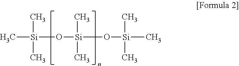
- the polydimethylsiloxane crosslinker may be a material represented by Formula 2 below:
- the non-ionic surfactant may be formed of any one of 4-(1,1,3,3-tetramethylbutyl)phenyl-polyethylene glycol, fatty alcohol-polyoxyethylene ether, polyoxyethylene sorbitan fatty acid esters, polyoxyethylene fatty acid ester, polyoxyethylene alkylether, sorbitan esters, glyceryl esters, glyceryl monostearate, polyethylene glycol, polypropylene glycol, polypropylene glycol esters, cetyl alcohol, cetostearyl alcohol, stearyl alcohol, or a combination thereof.
- the non-ionic surfactant may be formed of various materials without being limited to the aforementioned materials.
- non-ionic surfactant may be 4-(1,1,3,3-tetramethylbutyl)phenyl-polyethylene glycol represented by Formula 3 below:
- Bubbles in the dispersing solution 160 may be removed by degassing.
- the properties of the dispersing solution 160 may be controlled by a non-ionic surfactant included therein.
- the dispersing solution 160 may be spin-coated the substrate 110 coated with the metal nanowire network 150 , but the present disclosure is not limited to this coating manner.
- the dispersing solution 160 may be coated in other known manners varying a rotation speed and time.
- the dispersing solution 160 may be coated in a spin coating manner, a spray coating manner, an inkjet coating manner, a slit coating manner, a deep coating manner, or the like, without being specifically limited thereto.
- the dispersing solution 160 is spin-coated on the substrate 110 coated with the metal nanowire network 150 at 3 rpm to 400 rpm for 15 seconds to 30 seconds ( 130 b ), and then a heat hardening process ( 140 b ) is performed.
- the heat hardening may be performed at 40° C. to 80° C. for 8 hours to 12 hours, thereby forming the adhesive polydimethylsiloxane matrix 170 in which a nanowire network has been embedded.
- the heat-hardened adhesive silicone-based polymer matrix 170 is detached from the substrate 110 , thereby forming an adhesive transparent electrode 100 in which the metal nanowire network has been embedded.
- a silicone-based polymer matrix including a metal nanowire network on a surface thereof may be fabricated by heat-hardening a silicone-based polymer and then separating the hardened silicone-based polymer from a substrate, unlike a conventional method of forming an electrode on a heat-hardened polymer substrate in a coating process, etc. Accordingly, the adhesive transparent electrode based on the adhesive silicone-based polymer matrix according to an embodiment of the present disclosure may be simply formed without an additional process of forming an electrically conductive material.
- Dispersing solutions were prepared by mixing polydimethylsiloxane base, polydimethylsiloxane crosslinker, and 4-(1,1,3,3-tetramethylbutyl)phenyl-polyethylene glycol (hereinafter referred to as “Triton X-100”) in various weight ratios of 10:1:0 to 10:1:0.08.
- a weight ratio of the polydimethylsiloxane base to the polydimethylsiloxane crosslinker was fixed to 10:1.
- a slide glass (Paul Marienfeld GmbH & Co. KG, Germany), which was used as a substrate was sequentially washed with acetone, 2-propanol, and deionized water for 10 minutes in an ultrasonic bath, respectively.
- the washed slide glass was dried using an air gun.
- a dispersing solution was spin-coated on the substrate, coated with the silver nanowire solution, at 300 rpm for 15 seconds, followed by heat hardening at 40° C. to 80° C. for 11 hours.
- the hardened adhesive polydimethylsiloxane matrix was immersed in a bath containing deionized water for 5 minutes at room temperature, and then the adhesive transparent electrode, in which the nanowire network was embedded, was removed from the substrate in the state in which it was immersed in the deionized water.
- a dispersing solution was prepared by mixing a polydimethylsiloxane base and polydimethylsiloxane crosslinker in a weight ratio of 10:1.
- a slide glass (Paul Marienfeld GmbH & Co. KG, Germany), which was used as a substrate was sequentially washed with acetone, 2-propanol, and deionized water for 10 minutes in an ultrasonic bath, respectively.
- the washed slide glass was dried using an air gun.
- a dispersing solution was spin-coated on the substrate, coated with the silver nanowire solution, at 300 rpm for 15 seconds, followed by heat hardening at 40° C. to 80° C. for 11 hours.
- the hardened polydimethylsiloxane matrix was immersed in a bath containing deionized water for 5 minutes at room temperature, and then the polydimethylsiloxane matrix, in which the nanowire network was embedded, was removed from the substrate in the state in which it was immersed in the deionized water.
- Triton X-100 content (% by weight) in the adhesive polydimethylsiloxane matrix and hardening temperature (T a ) thereof were varied. Used samples are summarized in Table 1 below.
- FIGS. 2 A to 2 E illustrate adhesive polydimethylsiloxane matrix images dependent upon a Triton X-100 content in an adhesive polydimethylsiloxane matrix according to an embodiment of the present disclosure
- FIG. 2 F is a graph illustrating light transmittances dependent upon a Triton X-100 content in an adhesive polydimethylsiloxane matrix.
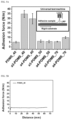
- a Triton X-100 content in the adhesive polydimethylsiloxane matrix was adjusted to 0%, 0.3%, 0.4%, 0.5%, and 0.8% at a heat hardening temperature of 40° C. As a result, it can be confirmed that light scattering of the adhesive polydimethylsiloxane matrix is worsened with increasing Triton X-100 content.
- a polydimethylsiloxane matrix (PDMS_40) excluding Triton X-100 exhibits a highest light transmittance value of 94.3% at a wavelength of 550 nm. It can be confirmed that light transmittance values of an adhesive polydimethylsiloxane matrix with 0.3% by weight of Triton X-100 (hereinafter referred to as “a3-PDMS_40”) and an adhesive polydimethylsiloxane matrix mixed with 0.4% by weight of Triton X-100 (hereinafter referred to as “a4-PDMS_40) are respectively 91.4% and 84.7% which are lower than that of PDMS_40.
- the adhesive polydimethylsiloxane matrix should have a light transmittance of 80% or more. Therefore, a3-PDMS_40 and a4-PDMS_40 were selected for subsequent analysis.
- Light transmittance is decreased with increasing Triton X-100 content because light scatters due to a micelle structure formed in a polydimethylsiloxane matrix mixed with Triton X-100. Since the polydimethylsiloxane matrix is very hydrophobic, alkyls in a Triton X-100 chain form a shell, whereas corresponding polyethylene glycol (PEG) forms a core of the micelle structure.
- PEG polyethylene glycol
- FIG. 3 A illustrates stress-strain curves of adhesive polydimethylsiloxane matrixes according to an embodiment of the present disclosure
- FIG. 3 B illustrates an image of a4-PDMS_40 under a uniaxial stretching test.
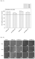
- Young's moduli and failure strains of a polydimethylsiloxane matrix, and adhesive polydimethylsiloxane matrixes which respectively included 0.3% by weight of Triton X-100 and 0.4% by weight of Triton X-100, fabricated while varying a heat hardening temperature at 40° C., 50° C. and 70° C. were only measured.
- a polydimethylsiloxane matrix sample and adhesive polydimethylsiloxane matrix samples used to measure Young's modulus and failure strain and measurement results thereof are summarized in Table 2 below.
- a3-PDMS_40 and a4-PDMS_40 exhibit the lowest Young's modulus and the highest failure strain among all the samples.
- Young's modulus and failure strain of PDMS_40 are respectively 500 kPa and 230%.
- a3-PDMS_40 and a4-PDMS_40 respectively exhibit Young's moduli of 38 kPa and 40 kPa, and both exhibit a failure strain of 400% or more.
- the Young's moduli of a3-PDMS_40 and a4-PDMS_40 are much lower than Young's modulus of human skin of 500 kPa to 1 MPa. From these results, it can be confirmed that a3-PDMS_40 and a4-PDMS_40 are suitable for epidermal electronics.
- Conformability of an electrode increases with decreasing Young's modulus of a polymer matrix. Accordingly, when the adhesive polydimethylsiloxane matrix has a lower Young's modulus than the skin, a contact area between an electrode and the skin expands, and a user feels more comfortable.
- a3-PDMS_40 and a4-PDMS_40 exhibit highly reinforced failure strain, which indicates that a3-PDMS_40 and a4-PDMS_40 are suitable candidate materials for a transparent and stretchable polymer matrix used in epidermal electronic devices.
- a4-PDMS_40 is not fractured even under a strain of 400% or more.
- FIG. 4 illustrates viscoelasticity of an adhesive polydimethylsiloxane matrix according to an embodiment of the present disclosure.
- Viscoelasticity of a polydimethylsiloxane matrix and adhesive polydimethylsiloxane matrixes was measured by means of a dynamic mechanical analyzer.
- the viscoelasticity of the polydimethylsiloxane matrix and the adhesive polydimethylsiloxane matrixes was determined according to Equation (1):
- tan ⁇ denotes a loss tangent
- E′ denotes elasticity of an elastic body
- E′′ denotes viscoelasticity of an elastic body. Accordingly, an elastic body exhibits higher viscoelasticity behavior as it has a higher loss tangent (tan ⁇ ).
- loss tangents of PDMS_40, a4-PDMS_40, a4-PDMS 50 , and a4-PDMS 70 increase with decreasing hardening temperature thereof.
- a4-PDMS_40 exhibits a high loss tangent of about 0.5 even at a low frequency of 0.1 Hz.
- the loss tangent of silicone rubber was reported to be less than 0.4 or less than 0.1. Accordingly, it can be confirmed that a4-PDMS_40 exhibits very high viscoelasticity, compared to other silicone-based elastic bodies.
- FIG. 5 A illustrates adhesion force of an adhesive polydimethylsiloxane matrix according to an embodiment of the present disclosure measured by a peel test
- FIGS. 5 B to 5 H illustrate adhesion force measured by a peel test
- FIG. 5 I illustrates images of an adhesive polydimethylsiloxane matrix supporting various weights.
- the size of a sample was 100 mm ⁇ 25 mm, a peeling speed was fixed to 300 mm min ⁇ 1 , and the force of a load cell was 20 N.
- a test environment was maintained at 25 ⁇ 2° C. under a relative humidity of 45 ⁇ 5%.
- a3-PDMS_40 and a4-PDMS_40 exhibit highest adhesion force among all the samples. It can be confirmed that the adhesion force of a3-PDMS_40 is 35 Nm ⁇ 1 which is 7 times higher than that of the polydimethylsiloxane matrix.
- heat hardening temperature affects the adhesion force of the adhesive polydimethylsiloxane matrix. It can be confirmed that the very low elastic modulus and the very high viscoelasticity of the adhesive polydimethylsiloxane matrix heat-hardened at 40° C. improve wetting and spreading of chains therein, which increases surface contact and the adhesion force of the adhesive polydimethylsiloxane matrix.
- FIGS. 6 A and 6 B illustrate a swelling ratio of an adhesive polydimethylsiloxane matrix according to an embodiment of the present disclosure
- FIGS. 6 C and 6 D illustrate a gel fraction.
- Optical properties of an adhesive polydimethylsiloxane matrix are greatly affected by a Triton X-100 content therein, and mechanical properties, such as Young's modulus, failure strain, viscoelasticity, and adhesion force, greatly affect a heat hardening temperature of an adhesive polydimethylsiloxane matrix.
- gel fractions of a4-PDMS_40 in chloroform and toluene are respectively 0.8 and 0.77, and gel fractions of PDMS_40 in chloroform and toluene are respectively 0.95 and 1.0.
- swelling ratios and gel fractions of a4-PDMS and PDMS_40 in chloroform and toluene solvents are represented by functions to hardening temperature, and the swelling ratios and the gel fractions are respectively determined by Equations (2) and (3) below:
- the swelling ratios of a4-PDMS_40 are respectively 2.5 times and 2 times higher than those of PDMS_40. Accordingly, the swelling ratio of the adhesive polydimethylsiloxane matrix is decreased with increasing heat hardening temperature, and becomes similar to that of the adhesive polydimethylsiloxane matrix at a heat hardening temperature of 70° C. or more.
- the gel fractions of a4-PDMS_40 in chloroform and toluene were respectively 0.8 and 0.77, and the gel fractions of PDMS_40 in chloroform and toluene were respectively 0.95 and 1.0. Similar to the swelling ratio result, the gel fraction of the adhesive polydimethylsiloxane matrix increases with increasing heat hardening temperature, and becomes similar to that of the polydimethylsiloxane matrix at a heat hardening temperature of 70° C. or more.
- Crosslinking of polydimethylsiloxane occurs via hydrosilylation using a platinum (Pt) catalyst.
- the Pt catalyst diffuses through a polydimethylsiloxane matrix to complete a crosslinking reaction.
- the Pt catalyst forms a complex with other polar functional groups, such as a PEG chain of Triton X-100, because it is coordinately unsaturated.
- Triton X-100 forms a core-shell structure inside a polydimethylsiloxane matrix. Therefore, when nonpolar functional groups surround platinum-interacting polar groups of Triton X-100 having a core-shell structure inside the polydimethylsiloxane matrix, the amount of an active Pt catalyst present in the polydimethylsiloxane matrix is reduced.
- crosslinking reaction is hindered by adding a small amount of Triton X-100 to a polydimethylsiloxane mixture to cause inactivation of a Pt catalyst, which is a main mechanism for forming a heterogeneously crosslinked network in polydimethylsiloxane. Due to Triton X-100 molecules, a heterogeneously crosslinked network composed of crosslinked polydimethylsiloxane and non-crosslinked polydimethylsiloxane is formed in the adhesive polydimethylsiloxane matrix.
- This composite structure modulates mechanical properties, such as Young's modulus, failure strain, viscoelasticity, and adhesion force, and thus, forms a soft and adhesive polydimethylsiloxane matrix.
- FIGS. 7 A and 7 B illustrate a result of a cell viability test and optical microscope images of fibroblasts to measure biocompatibility of an adhesive polydimethylsiloxane matrix according to an embodiment of the present disclosure
- FIG. 7 C is a graph illustrating absorbance of fibroblasts.
- a4-PDMS_40 and a4-PDMS_70 samples were used
- polydimethylsiloxane matrixes PDMS_40 and PDMS_70 were used
- cell viability and proliferation rates were analyzed by indirect methods.
- Fibroblasts L929) were grown at 37° C. in a 5% CO 2 incubator. The samples were washed with ethanol and by UV exposure. Subsequently, the samples were put in a 24-well plate, and then 1 ml of a solution containing fibroblasts was sprayed thereto.
- the density of the fibroblasts in the solution was 10 5 cells ⁇ ml ⁇ 1 , cell viability was analyzed using a CCK-8 kit, and absorbance was measured at 450 nm using a microplate reader (VersaMax, Molecular Devices LLC).
- Cell viability of a sample is determined by a ratio of the number of cells grown on a surface of the sample to the number of cells grown on a control sample (optimal environment conditions for cell growth). When a cell viability of a sample is 80% or more, the sample is considered biocompatible.
- Triton X-100 and low heat hardening temperature each independently induce decrease in a cell proliferation rate, and, particularly, the cell proliferation rate on a4-PDMS_40 is considerably low compared to other samples.
- a surface of a sample should be soft enough to allow cells to grow.
- a4-PDMS_40 has high surface roughness, thereby having a low cell proliferation rate.
- FIG. 8 is a graph illustrating light transmittance of an adhesive transparent electrode based on a silver nanowire-embedded adhesive polydimethylsiloxane matrix according to an embodiment of the present disclosure.
- an adhesive transparent electrode based on a silver nanowire-embedded adhesive polydimethylsiloxane matrix which has been heat-hardened at 40° C. and includes 0.4% by weight of Triton X-100, exhibits an electrical resistance (R S ) of 35 ⁇ sq ⁇ 1 and a light transmittance of about 75%.
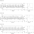
- FIG. 9 A is a graph illustrating a stretchability test result of an adhesive transparent electrode based on a silver nanowire-embedded adhesive polydimethylsiloxane matrix according to an embodiment of the present disclosure
- FIGS. 9 B and 9 C illustrate field emission-scanning electron microscopy (FE-SEM) images before and after stretching of a polydimethylsiloxane matrix-based transparent electrode (PDMS_40NW)
- FIGS. 9 D and 9 E illustrate FE-SEM images before and after stretching of an adhesive polydimethylsiloxane matrix-based transparent electrode (a4-PDMS_40NW).
- FE-SEM field emission-scanning electron microscopy
- a polydimethylsiloxane matrix-based transparent electrode sample (PDMS_40NW) and a a4-PDMS_40-based transparent electrode sample (a4-PDMS_40NW), which was an adhesive polydimethylsiloxane matrix, were used. This test was performed for 500 cycles at a strain of 12.5%.
- the a4-PDMS_40NW sample was only used because an a3-PDMS_40-based transparent electrode sample (a3-PDMS_40NW) exhibited too high electrical resistance to be applied to a transparent electrode.
- an electrical resistance ratio (R/R 0 ) of a4-PDMS_40NW decreases to 0.8 after 100 cycles and reaches 0.94 after 500 cycles.
- an electrical resistance ratio of PDMS_40NW continues to increase and reaches 1.5 after 500 cycles.
- FIGS. 9 B to 9 E enlarged portions of left images are illustrated in right images.
- PDMS_40NW shows severely peeled silver nanowires even before the periodic stretchability test.
- silver nanowires are fractured after the periodic stretchability test (indicated by dotted lines). From these images, it can be confirmed that the silver nanowires are not satisfactorily embedded in the polydimethylsiloxane matrix due to low adhesion force between the polydimethylsiloxane matrix and the silver nanowires.
- FIG. 9 D it can be confirmed that a4-PDMS_40NW does not show peeling of AgNWs.
- FIG. 9 E it can be confirmed that AgNWs are not fractured after the periodic stretchability test.
- the adhesion force between a4-PDMS_40 and silver nanowires is higher than that between PDMS_40 and silver nanowires because PEG chains of Triton X-100 can participate in electrostatic interactions with silver nanowires.
- Stretchability of the a4-PDMS_40NW electrode was improved due to superior adhesiveness between a4-PDMS_40 and silver nanowires.
- Another reason for the decrease in the electrical resistance ratio after stretching of 100 cycles is that alignment of silver nanowires has been changed in a stretching direction. According to previous research by other researchers, silver nanowires can be aligned in a stretching direction during mechanical stretching.
- the silver nanowires inserted in a4-PDMS_40 may be aligned in a stretching direction during periodic stretching because the adhesion force between silver nanowires and a4-PDMS_40 is strong due to Triton X-100.
- FIG. 10 A illustrates photograph of a strain sensor, to which a transparent electrode (a4-PDMS_40NW) based on a silver nanowire-embedded adhesive polydimethylsiloxane matrix according to an embodiment of the present disclosure is applied, attached to the wrist
- FIG. 10 B illustrates photographs of a strain sensor, to which an transparent electrode (PDMS_40NW) based on a silver nanowire-embedded polydimethylsiloxane matrix according to an embodiment of the present disclosure is applied, attached to the wrist.
- a4-PDMS_40NW exhibits perfectly conformal contact with the skin and is not peeled off by repeated bending of the wrist 10 times (a third image of FIG. 10 A ).
- the strain sensor, to which the PDMS_40NW is applied is peeled off from the skin even by a first bending motion (a second image of FIG. 10 B ).
- FIG. 10 C illustrates a relative resistance change of a strain sensor, to which a transparent electrode (a4-PDMS_40NW) based on a silver nanowire-embedded adhesive polydimethylsiloxane matrix according to an embodiment of the present disclosure is applied, and a relative resistance change of a strain sensor, to which an transparent electrode (PDMS_40NW) based on a silver nanowire-embedded polydimethylsiloxane matrix is applied.
- a transparent electrode a4-PDMS_40NW
- a relative resistance change of a strain sensor to which an transparent electrode (PDMS_40NW) based on a silver nanowire-embedded polydimethylsiloxane matrix is applied.
- a4-PDMS_40NW exhibits a greater electrical resistance change than PDMS_40NW under the same stain applied thereto. This indicates that the sensitivity of a4-PDMS_40NW is significantly higher than that of PDMS_40NW under the fixed strain. Such a difference is caused by higher conformability and stretchability of a4-PDMS_40NW to the skin, compared to PDMS_40NW.
- the strain sensor to which a4-PDMS_40NW is applied, exhibits low hysteresis, and maintains a relative resistance change ( ⁇ R ⁇ R 0 ⁇ 1 ) of 0 during the periodic bending of the wrist.
- the strain sensor to which PDMS_40NW is applied, exhibits high hysteresis that greatly deteriorates performance of the strain sensor, and ⁇ R ⁇ R 0 ⁇ 1 in a straight state continuously increases during multiple bending cycles of the wrist.
- FIGS. 11 A to 11 C illustrate photographs of ECG sensors, to which a transparent electrode (a4-PDMS_40NW) based on a silver nanowire-embedded adhesive polydimethylsiloxane matrix according to an embodiment of the present disclosure is applied, attached to an arm ( FIG. 11 A ) and photographs of ECG sensors, to which an transparent electrode (PDMS_40NW) based on a silver nanowire-embedded polydimethylsiloxane matrix is applied, attached to an arm, ( FIGS. 11 B and C) and FIG. 11 D illustrates skin impedances measured with the ECG sensors.
- ECG sensors to which a4-PDMS_40NW has been applied, are attached to the arm by a 3 cm interval so as to measure skin impedance, and are well attached to the arm without lifting.
- the ECG sensors can be confirmed to be well attached to the arm without lifting when observed at a different angle.
- FIG. 11 B it can be confirmed that, when the ECG sensors, to which PDMS_40NW has been applied, are attached to the arm without an adhesive tape, the ECG sensors have poor adhesiveness to the skin and thus are easily peeled off. Accordingly, to increase adhesion force thereof to the skin, ECG sensors, to which PDMS_40NW has been applied, were attached using an adhesive tape as shown in FIG. 11 C .
- the ECG sensors, to which PDMS_40NW has been applied have poor adhesion force to the skin and thus exhibit low conformability, thereby exhibiting a very high skin impedance.
- FIG. 11 E illustrates a photograph of the skin after detaching the transparent electrode (a4-PDMS_40NW) based on the silver nanowire-embedded adhesive polydimethylsiloxane matrix according to an embodiment of the present disclosure therefrom.
- a4-PDMS_40NW may be advantageously applied to an ECG sensor.
- FIG. 12 A illustrates electrode positions of an ECG sensor, to which a transparent electrode (a4-PDMS_40NW) based on a silver nanowire-embedded adhesive polydimethylsiloxane matrix according to an embodiment of the present disclosure is applied.
- three electrodes were respectively attached to a right side of the chest, a left side of the chest, and a lower right side of the thorax so as to measure an electrocardiogram.
- FIG. 12 B illustrates electrocardiogram signals measured with an ECG sensor to which a commercial gel is applied
- FIG. 12 C illustrates electrocardiogram signals measured with an ECG sensor to which an transparent electrode (PDMS_40NW) based on a silver nanowire-embedded polydimethylsiloxane matrix is applied
- FIG. 12 D illustrates electrocardiogram signals measured with an ECG sensor, to which an transparent electrode (PDMS_40NW) based on a silver nanowire-embedded polydimethylsiloxane matrix is applied, attached to the skin using an adhesive tape
- FIG. 12 E illustrates electrocardiogram signals measured with an ECG sensor to which a transparent electrode (a4-PDMS_40NW) based on a silver nanowire-embedded adhesive polydimethylsiloxane matrix is applied.
- a P wave of the ECG sensor, to which a commercial gel-based transparent electrode has been applied is weakly observed.
- some signals of the ECG sensor, to which PDMS_40NW has been applied exhibit low signal noise and such severe noise that a P wave could not be distinguished.
- FIG. 12 D it can be confirmed that, when the ECG sensor, to which PDMS_40NW has been applied, is attached to the skin using an adhesive tape to increase contact of PDMS_40NW to the skin, noise of an ECG signal is slightly reduced, compared to the ECG sensor, to which PDMS_40NW has been applied, illustrated in FIG. 12 C , but there is still signal noise.
- the ECG sensor to which a4-PDMS_40NW has been applied, exhibits much less ECG signal noise, compared to the ECG sensor to which a commercial gel-based transparent electrode has been applied, illustrated in FIG. 12 B .
- FIG. 13 A illustrate positions of ECG sensors to which a transparent electrode (a4-PDMS_40NW) based on a silver nanowire-embedded adhesive polydimethylsiloxane matrix according to an embodiment of the present disclosure is applied.
- FIG. 13 B illustrates electrocardiogram signals measured with an ECG sensor to which a commercial gel is applied
- FIG. 13 C illustrates electrocardiogram signals measured with an ECG sensor, to which an transparent electrode (PDMS_40NW) based on a silver nanowire-embedded polydimethylsiloxane matrix is applied, attached to the skin using an adhesive tape
- FIG. 13 D illustrates electrocardiogram signals measured with an ECG sensor to which a transparent electrode (a4-PDMS_40NW) based on a silver nanowire-embedded adhesive polydimethylsiloxane matrix is applied.
- FIGS. 13 B to 13 D it can be confirmed that, when an ECG sensor is attached to the chest, noise of ECG signals is large due to a distance between the electrode and the heart (see FIGS. 12 B to 12 E ).
- the ECG sensor to which a4-PDMS_40NW has been applied, exhibits clear and stable ECG signals similar to the ECG sensor to which a commercial gel-based transparent electrode has been applied.
- the ECG sensor to which a4-PDMS_40NW has been applied, exhibits low signal noise due to high conformability thereof to the skin and high electrical conductivity of silver nanowires embedded therein.
- the ECG sensor to which a4-PDMS_40NW has been applied, exhibits higher adhesion force to the skin, compared to the ECG sensor to which PDMS_40NW has been applied, and considerably increased biocompatibility, compared to the ECG sensor to which a commercial gel-based transparent electrode has been applied.
- a transparent electrode wherein a metal nanowire network is embedded in an adhesive silicone-based polymer matrix including a non-ionic surfactant has very high conformability when applied to an epidermal biosensor.
- the mechanical characteristics may be improved by adjusting hardening temperature and adding a non-ionic surfactant, Triton X-100, to cause interaction between a platinum (Pt) catalyst, present in a polydimethylsiloxane crosslinker, and polar functional groups, present in Triton X-100, and thus, hindering crosslinking reaction of polydimethylsiloxane.
- Triton X-100 a non-ionic surfactant
- a sensor to which the transparent electrode according to the present disclosure is applied may greatly increase detection sensitivity of various bio-signals such as EMG, EEG, and glucose.
- the transparent electrode may be used as an electrode material of, other than a biosensor, various wearable electronic devices such as a triboelectric nanogenerator, an optoelectronic device, a transparent film heater, and a wireless antenna.
- the properties of a silicone-based polymer can be easily controlled with a very small amount of non-ionic surfactant by using a non-ionic surfactant.
- a transparent electrode according to an embodiment of the present disclosure has high adhesiveness, the transparent electrode can be attached to the skin without an additional adhesive, and the adhesiveness of the transparent electrode can be maintained even after repeated detachment and attachment.
- the transparent electrode can be fabricated only through heat-hardening of a silicone-based polymer, unlike a conventional method of forming an electrode on a hardened polymer substrate in another coating process, etc.
- electrical conductivity can be maintained even under high strain due to the electrical characteristics of a metal nanowire network.
Landscapes
- Engineering & Computer Science (AREA)
- Life Sciences & Earth Sciences (AREA)
- Health & Medical Sciences (AREA)
- Physics & Mathematics (AREA)
- Chemical & Material Sciences (AREA)
- Nanotechnology (AREA)
- General Health & Medical Sciences (AREA)
- Microelectronics & Electronic Packaging (AREA)
- Power Engineering (AREA)
- Veterinary Medicine (AREA)
- Biophysics (AREA)
- Public Health (AREA)
- Biomedical Technology (AREA)
- Animal Behavior & Ethology (AREA)
- Molecular Biology (AREA)
- Condensed Matter Physics & Semiconductors (AREA)
- General Physics & Mathematics (AREA)
- Computer Hardware Design (AREA)
- Medical Informatics (AREA)
- Surgery (AREA)
- Heart & Thoracic Surgery (AREA)
- Pathology (AREA)
- Crystallography & Structural Chemistry (AREA)
- Manufacturing & Machinery (AREA)
- Optics & Photonics (AREA)
- Materials Engineering (AREA)
- Radiology & Medical Imaging (AREA)
- Electromagnetism (AREA)
- Bioinformatics & Cheminformatics (AREA)
- Nuclear Medicine, Radiotherapy & Molecular Imaging (AREA)
- Ceramic Engineering (AREA)
- Theoretical Computer Science (AREA)
- Dispersion Chemistry (AREA)
- Mathematical Physics (AREA)
- Composite Materials (AREA)
- Adhesives Or Adhesive Processes (AREA)
- Laminated Bodies (AREA)
- Adhesive Tapes (AREA)
Abstract
Description


| TABLE 1 | ||
| Triton X-100 content (% by | ||
| weight) in adhesive | Heat hardening | |
| Sample name | polydimethylsiloxane matrix | temperature (Tc) (° C.) |
| |
0 | 40 |
| |
70 | |
| a3-PDMS_40 | 0.3 | 40 |
| a3- |
50 | |
| a3- |
70 | |
| a4-PDMS_40 | 0.4 | 40 |
| a4- |
50 | |
| a4- |
70 | |
| a5-PDMS_40 | 0.5 | 40 |
| a8-PDMS_40 | 0.8 | 40 |
| TABLE 2 | ||||
| Sample | Young's modulus (kPa) | Failure strain (%) | ||
| PDMS_40 | 480 ± 30 | 230 | ||
| a3-PDMS_40 | 38 ± 6.3 | >400 | ||
| a4- |
40 ± 5 | >400 | ||
| a3-PDMS_50 | 194 ± 7.2 | >300 | ||
| a4-PDMS_50 | 162 ± 20 | >300 | ||
| a3- |
1000 ± 50 | 220 | ||
| a4-PDMS_70 | 810 ± 20 | 210 | ||
Claims (13)
Applications Claiming Priority (4)
| Application Number | Priority Date | Filing Date | Title |
|---|---|---|---|
| KR10-2018-0001504 | 2018-01-05 | ||
| KR20180001504 | 2018-01-05 | ||
| KR1020180065578A KR20190083947A (en) | 2018-01-05 | 2018-06-07 | Adhesive transparent electrode and method for manufacturing thereof |
| KR10-2018-0065578 | 2018-06-07 |
Publications (2)
| Publication Number | Publication Date |
|---|---|
| US20190214593A1 US20190214593A1 (en) | 2019-07-11 |
| US11653510B2 true US11653510B2 (en) | 2023-05-16 |
Family
ID=67141126
Family Applications (1)
| Application Number | Title | Priority Date | Filing Date |
|---|---|---|---|
| US16/169,174 Active 2042-01-18 US11653510B2 (en) | 2018-01-05 | 2018-10-24 | Adhesive transparent electrode and method of fabricating the same |
Country Status (1)
| Country | Link |
|---|---|
| US (1) | US11653510B2 (en) |
Families Citing this family (1)
| Publication number | Priority date | Publication date | Assignee | Title |
|---|---|---|---|---|
| CN113243920B (en) * | 2021-05-12 | 2023-06-13 | 北京石墨烯研究院 | Flexible skin-adhering electrode and preparation method and application thereof |
-
2018
- 2018-10-24 US US16/169,174 patent/US11653510B2/en active Active
Non-Patent Citations (6)
| Title |
|---|
| Communication dated Jun. 18, 2019, issued by the Korean Intellectual Property Office in corresponding Korean Application No. 10-2018-0065578. |
| Hojjat Madadi, et al., "Study the Effects of Different Surfactants on Hydrophilicity of Polydimethylsiloxane (PDMS)", Proceedings of the ASME 2012 11th Biennial Conference On Engineering Systems Design And Analysis ESDA2012, Nantes, France, Jul. 2-4, 2012 (5 pages total). |
| JinHoon Kim, et al., "Silver nanowire network embedded in polydimethylsiloxane as stretchable, transparent, and conductive substrates", Journal of Applied Polymer Science, 2016, pp. 1-7 (7 pages total). |
| Mei Ying Teo, et al., "Highly Stretchable and Highly Conductive PEDOT:PSS/Ionic Liquid Composite Transparent Electrodes for Solution-Processed Stretchable Electronics", ACS Applied Materials & Interfaces, 2017, vol. 9, pp. 819-826 (9 pages total). |
| Oytun et al. "Fabrication of solution-processable, highly transparent and conductive electrodes via layer-by-layer assembly of functional silver nanowires". Thin Solid Films 636 (May 2017). (Year: 2017). * |
| Razak et al. "A soft and conductive PDMS-PEG block copolymer as a compliant electrode for dielectric elastomers" 2015. (Year: 2015). * |
Also Published As
| Publication number | Publication date |
|---|---|
| US20190214593A1 (en) | 2019-07-11 |
Similar Documents
| Publication | Publication Date | Title |
|---|---|---|
| Wang et al. | Robust, self-adhesive, reinforced polymeric nanofilms enabling gas-permeable dry electrodes for long-term application | |
| CN102762740B (en) | Analyte sensors comprising blended membrane compositions and methods for making and using them | |
| Li et al. | Flexible and wearable healthcare sensors for visual reality health-monitoring | |
| KR102176764B1 (en) | Adhesive transparent electrode and method for manufacturing thereof | |
| Sun et al. | Water-resistant and underwater adhesive ion-conducting gel for motion-robust bioelectric monitoring | |
| JP5595038B2 (en) | Analyte sensor device and manufacturing method, composition and kit thereof | |
| US9309550B2 (en) | Analyte sensors having nanostructured electrodes and methods for making and using them | |
| Guiseppi-Elie | An implantable biochip to influence patient outcomes following trauma-induced hemorrhage | |
| Xia et al. | Intrinsically Electron Conductive, Antibacterial, and Anti‐swelling Hydrogels as Implantable Sensors for Bioelectronics | |
| TW201922764A (en) | Silicon-containing compound, urethane resin, stretchable film, and method for forming the same | |
| US20120088997A1 (en) | Implantable biochip for managing trauma--induced hemorrhage | |
| US11839700B2 (en) | Bio-electrode composition, bio-electrode, and method for manufacturing a bio-electrode | |
| TWI667248B (en) | Silicon-containing compound, urethane resin, stretchable film, and method for forming the same | |
| US11607162B2 (en) | Bio-electrode composition, bio-electrode, and method for manufacturing a bio-electrode | |
| CN107260655B (en) | Vitamin E modified silicon-based hydrogel contact lens drug-loading system and preparation method thereof | |
| US11653510B2 (en) | Adhesive transparent electrode and method of fabricating the same | |
| WO2015192064A1 (en) | Graphene-based nanosensor for identifying target analytes | |
| Wu et al. | Ultrathin, soft, bioresorbable organic electrochemical transistors for transient spatiotemporal mapping of brain activity | |
| Jung et al. | Carbon nanofiber-based wearable patches for bio-potential monitoring | |
| CN111366571B (en) | CsPbBr 3-Au-based flexible photoinduced enhanced Raman sensor and preparation and application thereof | |
| Kotanen et al. | Characterization of a wireless potentiostat for integration with a novel implantable biotransducer | |
| Hua et al. | Hydrogel-Based Bioelectronics and Their Applications in Health Monitoring | |
| US11839476B2 (en) | Bio-electrode composition, bio-electrode, and method for manufacturing a bio-electrode | |
| Patel et al. | Flexible three-dimensional electrochemical glucose sensor with improved sensitivity realized in hybrid polymer microelectromechanical systems technique | |
| CN109142485B (en) | Glucose sensor and preparation method thereof |
Legal Events
| Date | Code | Title | Description |
|---|---|---|---|
| AS | Assignment |
Owner name: INDUSTRY-ACADEMIC COOPERATION FOUNDATION, YONSEI UNIVERSITY, KOREA, REPUBLIC OF Free format text: ASSIGNMENT OF ASSIGNORS INTEREST;ASSIGNORS:PARK, JIN WOO;KIM, JIN HOON;REEL/FRAME:047298/0941 Effective date: 20180913 Owner name: INDUSTRY-ACADEMIC COOPERATION FOUNDATION, YONSEI U Free format text: ASSIGNMENT OF ASSIGNORS INTEREST;ASSIGNORS:PARK, JIN WOO;KIM, JIN HOON;REEL/FRAME:047298/0941 Effective date: 20180913 |
|
| FEPP | Fee payment procedure |
Free format text: ENTITY STATUS SET TO UNDISCOUNTED (ORIGINAL EVENT CODE: BIG.); ENTITY STATUS OF PATENT OWNER: SMALL ENTITY |
|
| FEPP | Fee payment procedure |
Free format text: ENTITY STATUS SET TO SMALL (ORIGINAL EVENT CODE: SMAL); ENTITY STATUS OF PATENT OWNER: SMALL ENTITY |
|
| STPP | Information on status: patent application and granting procedure in general |
Free format text: NON FINAL ACTION MAILED |
|
| STPP | Information on status: patent application and granting procedure in general |
Free format text: RESPONSE TO NON-FINAL OFFICE ACTION ENTERED AND FORWARDED TO EXAMINER |
|
| STPP | Information on status: patent application and granting procedure in general |
Free format text: NON FINAL ACTION MAILED |
|
| AS | Assignment |
Owner name: ASEN COMPANY, KOREA, REPUBLIC OF Free format text: ASSIGNMENT OF ASSIGNORS INTEREST;ASSIGNOR:INDUSTRY-ACADEMIC COOPERATION FOUNDATION, YONSEI UNIVERSITY;REEL/FRAME:063314/0108 Effective date: 20230413 |
|
| STCF | Information on status: patent grant |
Free format text: PATENTED CASE |