US11652476B2 - Pad-tracking circuit design to prevent leakage current during power ramp up or ramp down of output buffer - Google Patents
Pad-tracking circuit design to prevent leakage current during power ramp up or ramp down of output buffer Download PDFInfo
- Publication number
- US11652476B2 US11652476B2 US17/499,886 US202117499886A US11652476B2 US 11652476 B2 US11652476 B2 US 11652476B2 US 202117499886 A US202117499886 A US 202117499886A US 11652476 B2 US11652476 B2 US 11652476B2
- Authority
- US
- United States
- Prior art keywords
- pad
- voltage
- control signal
- transistor
- output buffer
- Prior art date
- Legal status (The legal status is an assumption and is not a legal conclusion. Google has not performed a legal analysis and makes no representation as to the accuracy of the status listed.)
- Active
Links
Images


Classifications
-
- H—ELECTRICITY
- H03—ELECTRONIC CIRCUITRY
- H03K—PULSE TECHNIQUE
- H03K19/00—Logic circuits, i.e. having at least two inputs acting on one output; Inverting circuits
- H03K19/0008—Arrangements for reducing power consumption
- H03K19/0013—Arrangements for reducing power consumption in field effect transistor circuits
-
- H—ELECTRICITY
- H03—ELECTRONIC CIRCUITRY
- H03K—PULSE TECHNIQUE
- H03K17/00—Electronic switching or gating, i.e. not by contact-making and –breaking
- H03K17/16—Modifications for eliminating interference voltages or currents
-
- H—ELECTRICITY
- H03—ELECTRONIC CIRCUITRY
- H03K—PULSE TECHNIQUE
- H03K19/00—Logic circuits, i.e. having at least two inputs acting on one output; Inverting circuits
- H03K19/0175—Coupling arrangements; Interface arrangements
- H03K19/0185—Coupling arrangements; Interface arrangements using field effect transistors only
- H03K19/018507—Interface arrangements
-
- H—ELECTRICITY
- H03—ELECTRONIC CIRCUITRY
- H03K—PULSE TECHNIQUE
- H03K17/00—Electronic switching or gating, i.e. not by contact-making and –breaking
- H03K17/16—Modifications for eliminating interference voltages or currents
- H03K17/161—Modifications for eliminating interference voltages or currents in field-effect transistor switches
- H03K17/165—Modifications for eliminating interference voltages or currents in field-effect transistor switches by feedback from the output circuit to the control circuit
-
- H—ELECTRICITY
- H03—ELECTRONIC CIRCUITRY
- H03K—PULSE TECHNIQUE
- H03K19/00—Logic circuits, i.e. having at least two inputs acting on one output; Inverting circuits
- H03K19/003—Modifications for increasing the reliability for protection
- H03K19/00315—Modifications for increasing the reliability for protection in field-effect transistor circuits
-
- H—ELECTRICITY
- H03—ELECTRONIC CIRCUITRY
- H03K—PULSE TECHNIQUE
- H03K19/00—Logic circuits, i.e. having at least two inputs acting on one output; Inverting circuits
- H03K19/007—Fail-safe circuits
-
- H—ELECTRICITY
- H03—ELECTRONIC CIRCUITRY
- H03K—PULSE TECHNIQUE
- H03K4/00—Generating pulses having essentially a finite slope or stepped portions
- H03K4/06—Generating pulses having essentially a finite slope or stepped portions having triangular shape
Definitions
- an output buffer and an input buffer are connected to the same pad, and the GPIO can be operate in an output mode, an input mode or a fail-safe mode.
- the output buffer when the GPIO operates in the output mode, the output buffer is enabled so that a signal can be outputted to another device via the pad; when the GPIO operates in the input mode, the output buffer is disabled; and when the GPIO operates in the fail-safe mode, the output buffer is disabled while no supply voltage is applied to the output buffer, and a high voltage is provided to the pad.
- the output buffer may have leakage current if the supply voltage ramps up or ramp down, that is the output buffer may have leakage when a switching operation between the input mode and the fail-safe mode.
- an output buffer comprising a first transistor, a second transistor and a pad-tracking circuit.
- the first transistor is coupled between a supply voltage and an output node, wherein the output node is coupled to a pad.
- the second transistor is coupled between the output node and a reference voltage.
- the pad-tracking circuit is coupled to the control circuit and the first transistor, and is configured to generate a gate control signal to a gate electrode of the first transistor.
- the output buffer is selectively operated in an input mode and a fail-safe mode, when the output buffer operates in the input mode, the pad-tracking circuit generates the gate control signal to disable the first transistor, and the second transistor is also disabled; and when the output buffer operates in the fail-safe mode, the first transistor is powered down, and the pad-tracking circuit generates the gate control signal to the gate electrode of the first transistor according to a voltage of the pad.
- the pad-tracking circuit When the output buffer switches between the input mode and the fail-safe mode and the supply voltage of the first transistor ramps up or ramps down, the pad-tracking circuit generates the gate control signal to the gate electrode of the first transistor according to the voltage of the pad.
- FIG. 1 is a diagram illustrating an output buffer operating in an output mode according to one embodiment of the present invention.
- FIG. 2 is a diagram illustrating the output buffer operating in an input mode according to one embodiment of the present invention.
- FIG. 3 is a diagram illustrating the output buffer operating in a fail-safe mode according to one embodiment of the present invention.
- FIG. 4 shows a conventional output buffer that a voltage at the pad has an IR drop when switching between the input mode and the fail-safe mode.
- FIG. 5 shows that no leakage current occurs in the embodiment of the present invention.
- FIG. 6 is a diagram illustrating the pad-tracking circuit according to one embodiment of the present invention.
- FIG. 7 is a diagram illustrating the first multiplexer and the second multiplexer when the output buffer operates in the input mode according to one embodiment of the present invention.
- FIG. 8 is a diagram illustrating the first multiplexer and the second multiplexer when the output buffer operates in the fail-safe mode according to one embodiment of the present invention.
- FIG. 9 is a diagram illustrating an output buffer according to another embodiment of the present invention.
- FIG. 1 is a diagram illustrating an output buffer 100 operating in an output mode according to one embodiment of the present invention.
- the output buffer 100 comprises a control circuit 110 , a pad-tracking circuit 120 , a P-type transistor MP 1 and an N-type transistor MN 1 , wherein the output buffer 100 is supplied by a supply voltage VDIO 1 and a reference voltage VSS, and the supply voltage VDIO 1 may be equal to a fixed high voltage VDDQ, and the reference voltage VSS may be equal to 0V.
- the output buffer 100 is coupled to a pad 104 , wherein the pad 104 is selectively coupled to a specific voltage provider 102 , wherein the specific voltage provider 100 is configured to selectively provide a supply voltage VDIO 2 to the pad 104 via a resistor R.
- the output buffer 100 When the output buffer 100 operates in the output mode, the output buffer 100 is configured to output a high voltage (i.e., logical value “1”) or a low voltage (i.e., logical value “0”) to the pad 104 , and the specific voltage provider 102 is disabled.
- the control circuit 110 receives two control signals VC_I and VC_E, wherein the control signal VC_E is used to indicate if the output buffer 100 operates in the output mode, and the control signal VC_I is used to control the output buffer 100 to output the high voltage or the low voltage.
- control circuit 110 determines the output mode, and if the control signal VC_I is equal to “0”, the control circuit 110 controls the pad-tracking circuit 120 to generate a gate control signal PG 1 having high voltage such as VDDQ to a gate of the transistor MP 1 , and to generate a bulk control signal PB 1 having high voltage such as VDDQ to a bulk of the transistor MP 1 , to disable transistor MP 1 ; and the control circuit 110 further generates a gate control signal NG 1 having high voltage such as VDDQ to a gate of the transistor MN 1 to enable the transistor MN 1 .
- the pad 104 has a low voltage such as 0V.
- the control circuit 110 controls the pad-tracking circuit 120 to generate the gate control signal PG 1 having low voltage such as 0V to the gate of the transistor MP 1 , and to generate the bulk control signal PB 1 having high voltage such as VDDQ to the bulk of the transistor MP 1 , to enable transistor MP 1 ; and the control circuit 110 further generates the gate control signal NG 1 having low voltage such as 0V to the gate of the transistor MN 1 to disable the transistor MN 1 .
- the pad 104 has a high voltage such as VDDQ.
- FIG. 2 is a diagram illustrating the output buffer 100 operating in an input mode according to one embodiment of the present invention.
- the output buffer 100 and the specific voltage provider 102 are disabled, and an input buffer (not shown) is configured to receive signal at the pad 104 .
- the control circuit 110 receives two control signals VC_I and VC_E, wherein the control signal VC_E is used to indicate if the output buffer 100 operates in the input mode.
- the control circuit 110 determines the output mode, and under the condition that a voltage VPAD at the pad 104 has lower voltage level such as 0V, regardless of whether the control signal VC_I is equal to 0 or 1, the control circuit 110 controls the pad-tracking circuit 120 to generate the gate control signal PG 1 having high voltage such as VDDQ to the gate of the transistor MP 1 , and to generate the bulk control signal PB 1 having high voltage such as VDDQ to the bulk of the transistor MP 1 , to disable transistor MP 1 ; and the control circuit 110 further generates the gate control signal NG 1 having low voltage such as 0V to the gate of the transistor MN 1 to disable the transistor MN 1 .
- the output buffer 100 does not provide any signal to the pad 104 .
- FIG. 3 is a diagram illustrating the output buffer 100 operating in a fail-safe mode according to one embodiment of the present invention.
- the control circuit 110 and the transistor MP 1 of the output buffer 100 are powered down (i.e., the supply voltage VDIO 1 becomes 0V)
- the specific voltage provider 102 is enabled to provide high voltage to the pad 104 (in this embodiment, the pad 104 has voltage VPAD which is much close to supply voltage VDIO 2 , and the supply voltage VDIO 2 may be equal to or higher than VDDQ)
- the pad-tracking circuit 120 can be supplied by the supply voltage VDIO 2 to generate the gate control signal PG 1 and the bulk control signal PB 1 based on the voltage VPAD at the pad 104 .
- the pad-tracking circuit 120 when the output buffer 100 operates in the fail-safe mode, the pad-tracking circuit 120 generates the gate control signal PG 1 and the bulk control signal PB 1 having the voltage VPAD to the transistor MP 1 , to disable the transistor MP 1 to prevent leakage current.
- VDDQ is provided by a voltage source, and VDDQ always has a high voltage level (fixed high voltage level) no matter if the output buffer 100 operates in the output mode and the input mode.
- the control circuit 110 when the output buffer 100 operates in the input mode, the control circuit 110 always controls the pad-tracking circuit 120 to generate the gate control signal PG 1 having VDDQ to disable the transistor MP 1 .
- the output buffer 100 switches between the input mode and the fail-safe mode, that is the supply voltage VDIO 1 increases from 0V to VDDQ or decreases from VDDQ to 0V, the transistor MP 1 may be enabled within a period of time, thus causing leakage current.
- the output buffer 100 switches between the input mode and the fail-safe mode, that is the supply voltage VDIO 1 increases from 0V to VDDQ or decreases from VDDQ to 0V
- the transistor MP 1 may be enabled within a period of time, thus causing leakage current.
- the pad-tracking circuit 120 is configured to always provide the voltage VPAD at the pad 104 as the gate control signal PG 1 and the bulk control signal PB 1 when the supply voltage VDIO 1 ramps up or ramps down, and there will be no leakage current between the pad 104 and the supply voltage VDIO 1 , as shown in FIG. 5 .
- FIG. 6 is a diagram illustrating the pad-tracking circuit 120 according to one embodiment of the present invention.
- the pad-tracking circuit 120 comprises a first multiplexer 610 and a second multiplexer 620 , wherein the first multiplexer 610 is configured to receive a plurality of input signals such as VDDQ and VPAD, and select one of the input signals as the gate control signal PG 1 according to a first selection signal SEL 1 ; and the second multiplexer 620 is configured to receive a plurality of input signals such as VDDQ and VPAD, and select one of the input signals as the bulk control signal PB 1 according to a second selection signal SEL 2 .
- the first multiplexer 610 outputs the voltage VPAD at the pad 104 as the gate control signal PG 1
- the second multiplexer 620 outputs the voltage VPAD at the pad 104 as the bulk control signal PB 1 . That is, if VPAD is a low voltage such as 0V, the gate control signal PG 1 and the bulk control signal PB 1 are equal to 0V; and if VPAD is a high voltage such as VDIO 2 /VDDQ, the gate control signal PG 1 and the bulk control signal PB 1 are equal to VDDQ.
- the first multiplexer 610 when the supply voltage VDIO 1 is equal to VDDQ and the output buffer 100 operates in the input mode, if VPAD is a low voltage such as 0V, the first multiplexer 610 outputs VDDQ at the pad 104 as the gate control signal PG 1 , and the second multiplexer 620 outputs VDDQ at the pad 104 as the bulk control signal PB 1 ; and if VPAD is a high voltage such as VDIO 2 /VDDQ, the first multiplexer 610 outputs VPAD at the pad 104 as the gate control signal PG 1 , and the second multiplexer 620 outputs VPAD at the pad 104 as the bulk control signal PB 1 .
- the first selection signal SEL 1 and the second selection signal SEL 2 can be any signal capable of indicating the level of VPAD.
- the pad-tracking circuit 120 when the pad 104 receives a high voltage such as VDIO 2 from the specific voltage provider 102 , the pad-tracking circuit 120 always provides the voltage VPAD at the pad 104 as the gate control signal PG 1 and the bulk control signal PB 1 , to prevent the leakage current of the transistor MP 1 when the supply voltage VDIO 1 ramps up or ramps down.
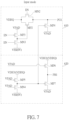
- FIG. 7 is a diagram illustrating the first multiplexer 610 and the second multiplexer 620 when the output buffer 100 operates in the input mode according to one embodiment of the present invention.
- the first multiplexer 610 comprises P-type transistors MP 2 -MP 4 and N-type transistors MN 2 -MN 3 , wherein the transistors MP 2 and MN 2 serve as a transmission gate to selectively output VDDQ as the gate control signal PG 1 , the transistors MP 3 and MN 3 are coupled between VPAD and VSS, and the transistor MP 4 is used to selectively outputs VPAD as the gate control signal PG 1 .
- the transistors MN 2 , MP 3 and MN 3 are controlled by an enable signal EN that is equal to 0V, the transistor MP 2 is controlled by an output signal of the transistors MP 3 and MN 3 .
- the second multiplexer 620 comprises P-type transistors MP 5 -MP 7 and an N-type transistor MN 4 , wherein the transistors MP 5 and MN 4 are coupled between the supply voltage VDIO 1 and VSS, the transistors MP 6 and MP 7 are coupled between the supply voltage VDIO 1 and VPAD.
- the transistors MP 5 , MN 4 and MP 6 are controlled by the voltage VPAD
- the transistor MP 7 is controlled by the output signal of the transistors MP 5 and MN 4
- the output signal of the transistors MP 5 and MN 4 are also used to control the transistor MP 4 of the first multiplexer 610
- an output signal of the transistors MP 6 and MP 7 serves as the bulk control signal PB 1 .
- the enable signal EN is equal to 0V, and when the voltage VPAD has a high voltage level such as VDDQ, the transistors MP 2 , MN 2 , MN 3 , MP 5 , MP 6 are disabled while the transistors MP 3 , MP 4 , MN 4 and MP 7 are enabled, so that the gate control signal PG 1 and the bulk control signal PB 1 are equal to VPAD.
- the transistors MN 2 , MN 3 , MP 4 , MN 4 and MP 7 are disabled while the transistors MP 2 , MP 3 , MP 5 and MP 6 are enabled, so that the gate control signal PG 1 and the bulk control signal PB 1 are equal to VDDQ.
- FIG. 8 is a diagram illustrating the first multiplexer 610 and the second multiplexer 620 when the output buffer 100 operates in the fail-safe mode according to one embodiment of the present invention. As shown in FIG. 8 , regardless of whether the voltage VPAD has high voltage level or low voltage level, the gate control signal PG 1 and the bulk control signal PB 1 are equal to VPAD.
- the pad-tracking circuit 120 may have other circuit designs.
- the output buffer 100 comprises only one P-type transistor MP 1 and only one N-type transistor MN 1 serving as an output stage, however, in other embodiment, the output stage may have more than one P-type transistor and/or more than one N-type transistor.
- the output stage comprises P-type transistors MP 1 -MPN and N-type transistors MN 1 -MNM connected in cascode, and the P-type transistors MP 1 -MPN and N-type transistors MN 1 -MNM are controlled by control signals PG 1 -PGM and NG 1 -NGM, respectively.
- the pad-tracking circuit when the output buffer switches between the input mode and the fail-safe mode, the pad-tracking circuit always provides the gate control signal that is substantially equal to the voltage of the pad to control the P-type transistor when the supply voltage ramps up or ramps down. Therefore, there will be no leakage current flowing through the P-type transistor when the supply voltage of the P-type transistor ramps up or ramps down.
Abstract
The present invention provides an output buffer including a first transistor, a second transistor and a pad-tracking circuit is disclosed. The first transistor is coupled between a supply voltage and an output node, wherein the output node is coupled to a pad. The second transistor is coupled between the output node and a reference voltage. The pad-tracking circuit is coupled to the control circuit and the first transistor, and is configured to generate a gate control signal to a gate electrode of the first transistor. The output buffer is selectively operated in an input mode and a fail-safe mode, and when the output buffer switches between the input mode and the fail-safe mode and the supply voltage of the first transistor ramps up or ramps down, the pad-tracking circuit generates the gate control signal to the gate electrode of the first transistor according to the voltage of the pad.
Description
This application claims the priority of U.S. Provisional Application No. 63/142,517, filed on Jan. 28, 2021, which is included herein by reference in its entirety.
In conventional general purpose input/output (GPIO) designs, an output buffer and an input buffer are connected to the same pad, and the GPIO can be operate in an output mode, an input mode or a fail-safe mode. Regarding three modes of the GPIO, when the GPIO operates in the output mode, the output buffer is enabled so that a signal can be outputted to another device via the pad; when the GPIO operates in the input mode, the output buffer is disabled; and when the GPIO operates in the fail-safe mode, the output buffer is disabled while no supply voltage is applied to the output buffer, and a high voltage is provided to the pad. In the above design, however, the output buffer may have leakage current if the supply voltage ramps up or ramp down, that is the output buffer may have leakage when a switching operation between the input mode and the fail-safe mode.
It is therefore an objective of the present invention to provide an output buffer design, which can prevent leakage current during power ramp up and power ramp down of the output buffer, to solve the above-mentioned problems.
According to one embodiment of the present invention, an output buffer comprising a first transistor, a second transistor and a pad-tracking circuit is disclosed. The first transistor is coupled between a supply voltage and an output node, wherein the output node is coupled to a pad. The second transistor is coupled between the output node and a reference voltage. The pad-tracking circuit is coupled to the control circuit and the first transistor, and is configured to generate a gate control signal to a gate electrode of the first transistor. The output buffer is selectively operated in an input mode and a fail-safe mode, when the output buffer operates in the input mode, the pad-tracking circuit generates the gate control signal to disable the first transistor, and the second transistor is also disabled; and when the output buffer operates in the fail-safe mode, the first transistor is powered down, and the pad-tracking circuit generates the gate control signal to the gate electrode of the first transistor according to a voltage of the pad. When the output buffer switches between the input mode and the fail-safe mode and the supply voltage of the first transistor ramps up or ramps down, the pad-tracking circuit generates the gate control signal to the gate electrode of the first transistor according to the voltage of the pad.
These and other objectives of the present invention will no doubt become obvious to those of ordinary skill in the art after reading the following detailed description of the preferred embodiment that is illustrated in the various figures and drawings.
Certain terms are used throughout the following description and claims to refer to particular system components. As one skilled in the art will appreciate, manufacturers may refer to a component by different names. This document does not intend to distinguish between components that differ in name but not function. In the following discussion and in the claims, the terms “including” and “comprising” are used in an open-ended fashion, and thus should be interpreted to mean “including, but not limited to . . . ”. The terms “couple” and “couples” are intended to mean either an indirect or a direct electrical connection. Thus, if a first device couples to a second device, that connection may be through a direct electrical connection, or through an indirect electrical connection via other devices and connections.
When the output buffer 100 operates in the output mode, the output buffer 100 is configured to output a high voltage (i.e., logical value “1”) or a low voltage (i.e., logical value “0”) to the pad 104, and the specific voltage provider 102 is disabled. Specifically, the control circuit 110 receives two control signals VC_I and VC_E, wherein the control signal VC_E is used to indicate if the output buffer 100 operates in the output mode, and the control signal VC_I is used to control the output buffer 100 to output the high voltage or the low voltage. In this embodiment, when the control signal VC_E is equal to “1”, the control circuit 110 determines the output mode, and if the control signal VC_I is equal to “0”, the control circuit 110 controls the pad-tracking circuit 120 to generate a gate control signal PG1 having high voltage such as VDDQ to a gate of the transistor MP1, and to generate a bulk control signal PB1 having high voltage such as VDDQ to a bulk of the transistor MP1, to disable transistor MP1; and the control circuit 110 further generates a gate control signal NG1 having high voltage such as VDDQ to a gate of the transistor MN1 to enable the transistor MN1. At this time, the pad 104 has a low voltage such as 0V. On the other hand, if the control signal VC_I is equal to “1”, the control circuit 110 controls the pad-tracking circuit 120 to generate the gate control signal PG1 having low voltage such as 0V to the gate of the transistor MP1, and to generate the bulk control signal PB1 having high voltage such as VDDQ to the bulk of the transistor MP1, to enable transistor MP1; and the control circuit 110 further generates the gate control signal NG1 having low voltage such as 0V to the gate of the transistor MN1 to disable the transistor MN1. At this time, the pad 104 has a high voltage such as VDDQ.
In the conventional art, when the output buffer 100 operates in the input mode, the control circuit 110 always controls the pad-tracking circuit 120 to generate the gate control signal PG1 having VDDQ to disable the transistor MP1. However, when the output buffer 100 switches between the input mode and the fail-safe mode, that is the supply voltage VDIO1 increases from 0V to VDDQ or decreases from VDDQ to 0V, the transistor MP1 may be enabled within a period of time, thus causing leakage current. Specifically, referring to FIG. 4 , when the supply voltage VDIO1 ramps up or ramps down, the gate control signal PG1 and the bulk control signal PB1 may be dropped and the transistor MP1 may be enabled so that a leakage current flowing from the pad 104 to the source electrode of the transistor MP1, causing the voltage VPAD has an IR drop. In order to solve this problem, the pad-tracking circuit 120 is configured to always provide the voltage VPAD at the pad 104 as the gate control signal PG1 and the bulk control signal PB1 when the supply voltage VDIO1 ramps up or ramps down, and there will be no leakage current between the pad 104 and the supply voltage VDIO1, as shown in FIG. 5 .
In the embodiment shown in FIG. 6 , no matter what mode it is (input mode or fail-safe mode), when the pad 104 receives a high voltage such as VDIO2 from the specific voltage provider 102, the pad-tracking circuit 120 always provides the voltage VPAD at the pad 104 as the gate control signal PG1 and the bulk control signal PB1, to prevent the leakage current of the transistor MP1 when the supply voltage VDIO1 ramps up or ramps down.
In the operation of the first multiplexer 610 and the second multiplexer 620 shown in FIG. 7 , the enable signal EN is equal to 0V, and when the voltage VPAD has a high voltage level such as VDDQ, the transistors MP2, MN2, MN3, MP5, MP6 are disabled while the transistors MP3, MP4, MN4 and MP7 are enabled, so that the gate control signal PG1 and the bulk control signal PB1 are equal to VPAD. In addition, when the voltage VPAD has a low voltage level such as 0V, the transistors MN2, MN3, MP4, MN4 and MP7 are disabled while the transistors MP2, MP3, MP5 and MP6 are enabled, so that the gate control signal PG1 and the bulk control signal PB1 are equal to VDDQ.
It is noted that the embodiment shown in FIGS. 6-8 are for illustration without a limitation of the present invention. In other embodiments, as long as the pad-tracking circuit 120 can always provide the voltage VPAD at the pad 104 as the gate control signal PG1 and the bulk control signal PB1 when the supply voltage VDIO1 ramps up and ramps down, the pad-tracking circuit 120 may have other circuit designs.
In the above embodiment shown in FIG. 1-3 , the output buffer 100 comprises only one P-type transistor MP1 and only one N-type transistor MN1 serving as an output stage, however, in other embodiment, the output stage may have more than one P-type transistor and/or more than one N-type transistor. Taking FIG. 9 as an example, the output stage comprises P-type transistors MP1-MPN and N-type transistors MN1-MNM connected in cascode, and the P-type transistors MP1-MPN and N-type transistors MN1-MNM are controlled by control signals PG1-PGM and NG1-NGM, respectively.
Briefly summarized, in the output buffer of the present invention, when the output buffer switches between the input mode and the fail-safe mode, the pad-tracking circuit always provides the gate control signal that is substantially equal to the voltage of the pad to control the P-type transistor when the supply voltage ramps up or ramps down. Therefore, there will be no leakage current flowing through the P-type transistor when the supply voltage of the P-type transistor ramps up or ramps down.
Those skilled in the art will readily observe that numerous modifications and alterations of the device and method may be made while retaining the teachings of the invention. Accordingly, the above disclosure should be construed as limited only by the metes and bounds of the appended claims.
Claims (12)
1. An output buffer, comprising:
a first transistor, coupled between a supply voltage and an output node, wherein the output node is coupled to a pad;
a second transistor, coupled between the output node and a reference voltage;
a pad-tracking circuit, coupled to the first transistor, configured to generate a gate control signal to a gate electrode of the first transistor;
wherein the output buffer is selectively operated in an input mode and a fail-safe mode, when the output buffer operates in the input mode, the pad-tracking circuit generates the gate control signal to disable the first transistor, and the second transistor is also disabled; and when the output buffer operates in the fail-safe mode, the first transistor is powered down, and the pad-tracking circuit generates the gate control signal to the gate electrode of the first transistor according to a voltage of the pad;
wherein when the output buffer switches between the input mode and the fail-safe mode, and the supply voltage of the first transistor ramps up or ramps down, the pad-tracking circuit generates the gate control signal to the gate electrode of the first transistor according to the voltage of the pad;
wherein when the output buffer operates in the input mode different from the fail-safe mode: the supply voltage has a fixed voltage level; and if the voltage of the pad has a high voltage level equal to the fixed voltage level of the supply voltage, the pad-tracking circuit refers to the voltage of the pad to generate the gate control signal, and a voltage level of the gate control signal is substantially equal to the voltage of the pad; and if the voltage of the pad has a low voltage level, the pad-tracking circuit refers to the supply voltage having the fixed voltage level to generate the gate control signal, and the voltage level of the gate control signal is substantially equal to the voltage of the supply voltage having the fixed voltage level.
2. The output buffer of claim 1 , wherein the when the output buffer switches between the input mode and the fail-safe mode and the supply voltage of the first transistor ramps up or ramps down, the pad-tracking circuit always generates the gate control signal to the gate electrode of the first transistor according to the voltage of the pad, and a voltage level of the gate control signal is substantially equal to the voltage of the pad.
3. The output buffer of claim 1 , wherein when the output buffer switches between the input mode and the fail-safe mode and the supply voltage of the first transistor ramps up or ramps down, the pad-tracking circuit generates a bulk control signal to a bulk of the first transistor according to the voltage of the pad.
4. The output buffer of claim 3 , wherein when the output buffer switches between the input mode and the fail-safe mode and the supply voltage of the first transistor ramps up or ramps down, the pad-tracking circuit always generates the gate control signal and the bulk control signal to the gate electrode and the bulk of the first transistor according to the voltage of the pad, and a voltage level of the gate control signal and a voltage of the bulk control signal are substantially equal to the voltage of the pad.
5. An output buffer, comprising:
a first transistor, coupled between a supply voltage and an output node, wherein the output node is coupled to a pad;
a second transistor, coupled between the output node and a reference voltage;
a pad-tracking circuit, coupled to the first transistor, configured to generate a gate control signal to a gate electrode of the first transistor;
wherein the output buffer is selectively operated in an input mode and a fail-safe mode, when the output buffer operates in the input mode, the pad-tracking circuit generates the gate control signal to disable the first transistor, and the second transistor is also disabled; and when the output buffer operates in the fail-safe mode, the first transistor is powered down, and the pad-tracking circuit generates the gate control signal to the gate electrode of the first transistor according to a voltage of the pad;
wherein when the output buffer switches between the input mode and the fail-safe mode, and the supply voltage of the first transistor ramps up or ramps down, the pad-tracking circuit generates the gate control signal to the gate electrode of the first transistor according to the voltage of the pad;
wherein when the output buffer operates in the input mode different from the fail-safe mode: the supply voltage has a fixed voltage level; and if the voltage of the pad has a high voltage level equal to the fixed voltage level of the supply voltage, the pad-tracking circuit refers to the voltage of the pad to generate the gate control signal and a bulk control signal, and voltage levels of the gate control signal and the bulk control signal are substantially equal to the voltage of the pad; and if the voltage of the pad has a low voltage level, the pad-tracking circuit refers to the supply voltage having the fixed voltage level to generate the gate control signal and the bulk control signal, and the voltage levels of the gate control signal and the bulk control signal are substantially equal to the voltage of the supply voltage having the fixed voltage level.
6. The output buffer of claim 5 , wherein the when the output buffer switches between the input mode and the fail-safe mode and the supply voltage of the first transistor ramps up or ramps down, the pad-tracking circuit always generates the gate control signal to the gate electrode of the first transistor according to the voltage of the pad, and a voltage level of the gate control signal is substantially equal to the voltage of the pad.
7. The output buffer of claim 5 , wherein when the output buffer switches between the input mode and the fail-safe mode and the supply voltage of the first transistor ramps up or ramps down, the pad-tracking circuit generates a bulk control signal to a bulk of the first transistor according to the voltage of the pad.
8. An output buffer, comprising:
a first transistor, coupled between a supply voltage and an output node, wherein the output node is coupled to a pad;
a second transistor, coupled between the output node and a reference voltage;
a pad-tracking circuit, coupled to the first transistor, configured to generate a gate control signal to a gate electrode of the first transistor;
wherein the output buffer is selectively operated in an input mode and a fail-safe mode, when the output buffer operates in the input mode, the pad-tracking circuit generates the gate control signal to disable the first transistor, and the second transistor is also disabled; and when the output buffer operates in the fail-safe mode, the first transistor is powered down, and the pad-tracking circuit generates the gate control signal to the gate electrode of the first transistor according to a voltage of the pad;
wherein when the output buffer switches between the input mode and the fail-safe mode, and the supply voltage of the first transistor ramps up or ramps down, the pad-tracking circuit generates the gate control signal to the gate electrode of the first transistor according to the voltage of the pad;
wherein when the output buffer operates in the input mode, the supply voltage has a fixed voltage level; and the pad-tracking circuit refers to the voltage of the pad to determine if generating the gate control signal according to the voltage of the pad or generating the gate control signal according to the supply voltage having the fixed voltage level;
wherein the pad-tracking circuit comprises:
a first multiplexer, configured to receive a plurality of input signals, and select one of the plurality of input signals to serve as the gate control signal, wherein the plurality of input signals comprises a first input signal having the fixed voltage level and a second input signal having the voltage of the pad;
wherein when the output buffer operates in the input mode different from the fail-safe mode: the supply voltage has a fixed voltage level; and if the voltage of the pad has a high voltage level equal to the fixed voltage level of the supply voltage, the first multiplexer selects the second input signal as the gate control signal; and if the voltage of the pad has a low voltage level, the first multiplexer selects the first input signal as the gate control signal.
9. The output buffer of claim 8 , wherein the pad-tracking circuit refers to the voltage of the pad to determine if generating a bulk control signal to a bulk of the first transistor according to the voltage of the pad or generating the bulk control signal according to the supply voltage having the fixed voltage level; and the pad-tracking circuit comprises:
a second multiplexer, configured to receive the plurality of input signals, and select one of the plurality of input signals to serve as the bulk control signal.
10. The output buffer of claim 8 , wherein when the output buffer operates in the fail-safe mode: if the voltage of the pad has the high voltage level, the first multiplexer outputs the second input signal to serve as the gate control signal.
11. The output buffer of claim 9 , wherein when the output buffer operates in the input mode: if the voltage of the pad has the high voltage level, the first multiplexer outputs the second input signal to serve as the gate control signal, and the second multiplexer outputs one of the plurality of input signals whose voltage level is equal to the second input signal to serve as the bulk control signal.
12. The output buffer of claim 9 , wherein when the output buffer operates in the input mode: if the voltage of the pad has the low voltage level, the first multiplexer outputs the first input signal to serve as the gate control signal, and the second multiplexer outputs one of the plurality of input signals whose voltage level is equal to the first input signal to serve as the bulk control signal.
Priority Applications (3)
| Application Number | Priority Date | Filing Date | Title |
|---|---|---|---|
| US17/499,886 US11652476B2 (en) | 2021-01-28 | 2021-10-13 | Pad-tracking circuit design to prevent leakage current during power ramp up or ramp down of output buffer |
| CN202111421319.8A CN114826245A (en) | 2021-01-28 | 2021-11-26 | Output buffer |
| TW110144776A TWI792734B (en) | 2021-01-28 | 2021-12-01 | Output buffer |
Applications Claiming Priority (2)
| Application Number | Priority Date | Filing Date | Title |
|---|---|---|---|
| US202163142517P | 2021-01-28 | 2021-01-28 | |
| US17/499,886 US11652476B2 (en) | 2021-01-28 | 2021-10-13 | Pad-tracking circuit design to prevent leakage current during power ramp up or ramp down of output buffer |
Publications (2)
| Publication Number | Publication Date |
|---|---|
| US20220239290A1 US20220239290A1 (en) | 2022-07-28 |
| US11652476B2 true US11652476B2 (en) | 2023-05-16 |
Family
ID=82495950
Family Applications (1)
| Application Number | Title | Priority Date | Filing Date |
|---|---|---|---|
| US17/499,886 Active US11652476B2 (en) | 2021-01-28 | 2021-10-13 | Pad-tracking circuit design to prevent leakage current during power ramp up or ramp down of output buffer |
Country Status (3)
| Country | Link |
|---|---|
| US (1) | US11652476B2 (en) |
| CN (1) | CN114826245A (en) |
| TW (1) | TWI792734B (en) |
Citations (19)
| Publication number | Priority date | Publication date | Assignee | Title |
|---|---|---|---|---|
| US5966026A (en) | 1995-02-14 | 1999-10-12 | Advanced Micro Devices, Inc. | Output buffer with improved tolerance to overvoltage |
| US6184700B1 (en) * | 1999-05-25 | 2001-02-06 | Lucent Technologies, Inc. | Fail safe buffer capable of operating with a mixed voltage core |
| US6696867B2 (en) | 1997-05-30 | 2004-02-24 | Micron Technology, Inc. | Voltage generator with stability indicator circuit |
| US6970024B1 (en) * | 2004-02-24 | 2005-11-29 | Altera Corporation | Over-voltage protection of integrated circuit I/O pins |
| US20080068050A1 (en) * | 2001-01-09 | 2008-03-20 | Broadcom Corporation | Sub-micron high input voltage tolerant input output (I/O) circuit |
| US7633321B2 (en) * | 2007-07-24 | 2009-12-15 | Infineon Technologies Ag | Driver circuit; electronic circuit having driver circuit and corresponding method |
| US20100253392A1 (en) * | 2009-04-03 | 2010-10-07 | Ming-Dou Ker | I/o buffer with twice the supply voltage tolerance using normal supply voltage devices |
| US7834653B1 (en) | 2009-10-31 | 2010-11-16 | Lsi Corporation | Failsafe and tolerant driver architecture and method |
| US7986171B2 (en) * | 2008-10-21 | 2011-07-26 | Himax Technologies Limited | Mixed-voltage I/O buffer |
| TWI406500B (en) | 2009-10-31 | 2013-08-21 | Lsi Corp | Bias voltage generation to protect input/output (io) circuits during a failsafe operation and a tolerant operation |
| US8598941B2 (en) | 2011-06-21 | 2013-12-03 | Lsi Corporation | Hybrid impedance compensation in a buffer circuit |
| US9432005B2 (en) * | 2014-06-12 | 2016-08-30 | Taiwan Semiconductor Manufacturing Company, Ltd. | Pull-up circuit and related method |
| US9738738B2 (en) * | 2015-04-01 | 2017-08-22 | Bridgestone Corporation | Polymers functionalized with activated nitrogen heterocycles containing a pendant functional group |
| US20190305778A1 (en) | 2018-04-02 | 2019-10-03 | Mediatek Inc. | Pad tracking circuit for high-voltage input-tolerant output buffer |
| US10644701B1 (en) * | 2019-05-21 | 2020-05-05 | Faraday Technology Corp. | Input and output circuit and self-biased circuit thereof |
| US20200145002A1 (en) * | 2018-11-02 | 2020-05-07 | Texas Instruments Incorporated | Failsafe, ultra-wide voltage input output interface using low-voltage gate oxide transistors |
| US10673436B1 (en) * | 2018-11-30 | 2020-06-02 | Texas Instruments Incorporated | Failsafe device |
| US10985754B1 (en) * | 2020-05-27 | 2021-04-20 | Db Hitek Co., Ltd. | Input/output circuit and electronic device including the same |
| US20210208615A1 (en) * | 2020-01-06 | 2021-07-08 | Arm Limited | Voltage Tracking Circuitry |
-
2021
- 2021-10-13 US US17/499,886 patent/US11652476B2/en active Active
- 2021-11-26 CN CN202111421319.8A patent/CN114826245A/en active Pending
- 2021-12-01 TW TW110144776A patent/TWI792734B/en active
Patent Citations (19)
| Publication number | Priority date | Publication date | Assignee | Title |
|---|---|---|---|---|
| US5966026A (en) | 1995-02-14 | 1999-10-12 | Advanced Micro Devices, Inc. | Output buffer with improved tolerance to overvoltage |
| US6696867B2 (en) | 1997-05-30 | 2004-02-24 | Micron Technology, Inc. | Voltage generator with stability indicator circuit |
| US6184700B1 (en) * | 1999-05-25 | 2001-02-06 | Lucent Technologies, Inc. | Fail safe buffer capable of operating with a mixed voltage core |
| US20080068050A1 (en) * | 2001-01-09 | 2008-03-20 | Broadcom Corporation | Sub-micron high input voltage tolerant input output (I/O) circuit |
| US6970024B1 (en) * | 2004-02-24 | 2005-11-29 | Altera Corporation | Over-voltage protection of integrated circuit I/O pins |
| US7633321B2 (en) * | 2007-07-24 | 2009-12-15 | Infineon Technologies Ag | Driver circuit; electronic circuit having driver circuit and corresponding method |
| US7986171B2 (en) * | 2008-10-21 | 2011-07-26 | Himax Technologies Limited | Mixed-voltage I/O buffer |
| US20100253392A1 (en) * | 2009-04-03 | 2010-10-07 | Ming-Dou Ker | I/o buffer with twice the supply voltage tolerance using normal supply voltage devices |
| US7834653B1 (en) | 2009-10-31 | 2010-11-16 | Lsi Corporation | Failsafe and tolerant driver architecture and method |
| TWI406500B (en) | 2009-10-31 | 2013-08-21 | Lsi Corp | Bias voltage generation to protect input/output (io) circuits during a failsafe operation and a tolerant operation |
| US8598941B2 (en) | 2011-06-21 | 2013-12-03 | Lsi Corporation | Hybrid impedance compensation in a buffer circuit |
| US9432005B2 (en) * | 2014-06-12 | 2016-08-30 | Taiwan Semiconductor Manufacturing Company, Ltd. | Pull-up circuit and related method |
| US9738738B2 (en) * | 2015-04-01 | 2017-08-22 | Bridgestone Corporation | Polymers functionalized with activated nitrogen heterocycles containing a pendant functional group |
| US20190305778A1 (en) | 2018-04-02 | 2019-10-03 | Mediatek Inc. | Pad tracking circuit for high-voltage input-tolerant output buffer |
| US20200145002A1 (en) * | 2018-11-02 | 2020-05-07 | Texas Instruments Incorporated | Failsafe, ultra-wide voltage input output interface using low-voltage gate oxide transistors |
| US10673436B1 (en) * | 2018-11-30 | 2020-06-02 | Texas Instruments Incorporated | Failsafe device |
| US10644701B1 (en) * | 2019-05-21 | 2020-05-05 | Faraday Technology Corp. | Input and output circuit and self-biased circuit thereof |
| US20210208615A1 (en) * | 2020-01-06 | 2021-07-08 | Arm Limited | Voltage Tracking Circuitry |
| US10985754B1 (en) * | 2020-05-27 | 2021-04-20 | Db Hitek Co., Ltd. | Input/output circuit and electronic device including the same |
Also Published As
| Publication number | Publication date |
|---|---|
| US20220239290A1 (en) | 2022-07-28 |
| CN114826245A (en) | 2022-07-29 |
| TWI792734B (en) | 2023-02-11 |
| TW202230982A (en) | 2022-08-01 |
Similar Documents
| Publication | Publication Date | Title |
|---|---|---|
| US6049245A (en) | Power reduction circuit | |
| US10305474B2 (en) | High voltage output driver with low voltage devices | |
| US5844425A (en) | CMOS tristate output buffer with having overvoltage protection and increased stability against bus voltage variations | |
| US7388410B2 (en) | Input circuits configured to operate using a range of supply voltages | |
| US7382158B2 (en) | Level shifter circuit | |
| US20080024178A1 (en) | Transmission line drivers and serial interface data transmission devices including the same | |
| US5801550A (en) | Output circuit device preventing overshoot and undershoot | |
| US8339159B2 (en) | Input buffer circuit of semiconductor apparatus | |
| US7956654B2 (en) | Predriver and output driver circuit using the same | |
| US7868667B2 (en) | Output driving device | |
| KR20040108011A (en) | An internal voltage generator for a semiconductor device | |
| US11799482B2 (en) | Interface circuit and semiconductor output circuit device | |
| US7282953B2 (en) | Pre-buffer level shifter and input/output buffer apparatus | |
| US11652476B2 (en) | Pad-tracking circuit design to prevent leakage current during power ramp up or ramp down of output buffer | |
| US6326803B1 (en) | Terminating circuit for a transmission line | |
| US5418477A (en) | Data output buffer pull-down circuit for TTL interface | |
| US10903840B2 (en) | Pad tracking circuit for high-voltage input-tolerant output buffer | |
| US10622976B2 (en) | Schmitt trigger circuit | |
| US6133755A (en) | Input/output buffer with reduced ring-back effect | |
| US6456147B1 (en) | Output interface circuit | |
| US6798236B2 (en) | Output buffer circuit with power supply voltages different from a power supply voltage applied to an internal circuit | |
| JP2001339285A (en) | Power-off detecting circuit | |
| US5825221A (en) | Output circuit of semiconductor device | |
| US20040001551A1 (en) | Data transmission circuit and method for reducing leakage current | |
| US7733154B2 (en) | Semiconductor device |
Legal Events
| Date | Code | Title | Description |
|---|---|---|---|
| AS | Assignment |
Owner name: MEDIATEK INC., TAIWAN Free format text: ASSIGNMENT OF ASSIGNORS INTEREST;ASSIGNORS:HSU, HSIN-CHENG;WU, CHIEN;REEL/FRAME:057771/0922 Effective date: 20210914 |
|
| FEPP | Fee payment procedure |
Free format text: ENTITY STATUS SET TO UNDISCOUNTED (ORIGINAL EVENT CODE: BIG.); ENTITY STATUS OF PATENT OWNER: LARGE ENTITY |
|
| STPP | Information on status: patent application and granting procedure in general |
Free format text: FINAL REJECTION MAILED |
|
| STPP | Information on status: patent application and granting procedure in general |
Free format text: DOCKETED NEW CASE - READY FOR EXAMINATION |
|
| STCF | Information on status: patent grant |
Free format text: PATENTED CASE |