US11631927B2 - Probe calibration system and method for electromagnetic compatibility testing - Google Patents
Probe calibration system and method for electromagnetic compatibility testing Download PDFInfo
- Publication number
- US11631927B2 US11631927B2 US16/458,004 US201916458004A US11631927B2 US 11631927 B2 US11631927 B2 US 11631927B2 US 201916458004 A US201916458004 A US 201916458004A US 11631927 B2 US11631927 B2 US 11631927B2
- Authority
- US
- United States
- Prior art keywords
- air
- cpw
- dielectric
- trace
- gcpw
- Prior art date
- Legal status (The legal status is an assumption and is not a legal conclusion. Google has not performed a legal analysis and makes no representation as to the accuracy of the status listed.)
- Active, expires
Links
Images


Classifications
-
- H—ELECTRICITY
- H01—ELECTRIC ELEMENTS
- H01P—WAVEGUIDES; RESONATORS, LINES, OR OTHER DEVICES OF THE WAVEGUIDE TYPE
- H01P1/00—Auxiliary devices
- H01P1/16—Auxiliary devices for mode selection, e.g. mode suppression or mode promotion; for mode conversion
-
- H—ELECTRICITY
- H01—ELECTRIC ELEMENTS
- H01P—WAVEGUIDES; RESONATORS, LINES, OR OTHER DEVICES OF THE WAVEGUIDE TYPE
- H01P3/00—Waveguides; Transmission lines of the waveguide type
- H01P3/003—Coplanar lines
- H01P3/006—Conductor backed coplanar waveguides
-
- H—ELECTRICITY
- H01—ELECTRIC ELEMENTS
- H01P—WAVEGUIDES; RESONATORS, LINES, OR OTHER DEVICES OF THE WAVEGUIDE TYPE
- H01P3/00—Waveguides; Transmission lines of the waveguide type
- H01P3/12—Hollow waveguides
- H01P3/121—Hollow waveguides integrated in a substrate
-
- H—ELECTRICITY
- H01—ELECTRIC ELEMENTS
- H01P—WAVEGUIDES; RESONATORS, LINES, OR OTHER DEVICES OF THE WAVEGUIDE TYPE
- H01P5/00—Coupling devices of the waveguide type
- H01P5/08—Coupling devices of the waveguide type for linking dissimilar lines or devices
-
- H—ELECTRICITY
- H01—ELECTRIC ELEMENTS
- H01P—WAVEGUIDES; RESONATORS, LINES, OR OTHER DEVICES OF THE WAVEGUIDE TYPE
- H01P11/00—Apparatus or processes specially adapted for manufacturing waveguides or resonators, lines, or other devices of the waveguide type
- H01P11/001—Manufacturing waveguides or transmission lines of the waveguide type
- H01P11/003—Manufacturing lines with conductors on a substrate, e.g. strip lines, slot lines
-
- H—ELECTRICITY
- H01—ELECTRIC ELEMENTS
- H01P—WAVEGUIDES; RESONATORS, LINES, OR OTHER DEVICES OF THE WAVEGUIDE TYPE
- H01P3/00—Waveguides; Transmission lines of the waveguide type
- H01P3/02—Waveguides; Transmission lines of the waveguide type with two longitudinal conductors
- H01P3/06—Coaxial lines
Definitions
- Electromagnetic compatibility (EMC) testing is widely performed on equipment, such as complete systems, integrated circuits, printed circuit boards (PCBs) and other electronic modules, to determine whether the equipment radiates more radio frequency (RF) energy than either allowed by regulations or acceptable to avoid interference with wireless receivers, or to determine if the equipment is susceptible to electromagnetic (EM) disturbances.
- An EMC test may involve a number of different EM analyses. As an example, EMC testing may involve radiating electromagnetic waves at the equipment, measuring the emissions from the equipment or testing the immunity to electrostatic discharges (ESD).
- Electromagnetic interference (EMI) testing is usually performed according to standards, e.g., the Federal Communications Commission (FCC) normally uses a semi-anechoic chamber or an open area test site to measure the fields in the far field region. Such methodology, however, provides little insight into the root cause of EMI problems.
- EMI analysis can also be performed by near-field scanning, i.e., measuring local electric or magnetic field around the equipment under test (EUT) to identify areas of strong electric or magnetic field. This near-field information may then assist in identifying the cause of an EMI problem of the EUT based on an implicit assumption that an area of strong field is the cause of the EMI problem.
- An immunity or ESD analysis can also be performed by subjecting the EUT to strong electromagnetic fields (immunity) or injecting ESD currents into the EUT at different locations. Such analysis can then include determining whether an error has occurred because of the RF field or ESD current stress injected into the selected location.
- the difference between the immunity analysis and the ESD analysis is the type of noise injected. Modulated RF signals are usually injected for the immunity analysis, whereas narrow pulses (having one or sub nanosecond rise time) are injected for an ESD analysis. Another relevant difference is that immunity analysis subjects the EUT to fields, most often in the far-field region of the transmitting antenna, while ESD testing injects currents directly into the EUT. Indirect ESD testing, which subjects the EUT only to the fields of the ESD, is also performed.
- a method that provides better insight into the possible root cause of an immunity or susceptibility problem is susceptibility scanning.
- a probe is moved above the equipment (e.g., PCB, cables etc.) and a strong local field is caused by injecting pulses or RF signals into the probe.
- the probe is moved around the equipment and the reaction of the equipment is observed. This way, local areas of higher susceptibility can be identified.
- strong local fields might be the cause of strong radiated emissions
- local areas of high susceptibility might be the reason for immunity or ESD problems as they show up if the complete system is tested in accordance to the standards, such as IEC 61000-4-3 (radiated immunity) or IEC 61000-4-2 (ESD).
- NFS Phase-resolved near-field scanning
- various technologies e.g., high speed communication systems, cloud computing, autonomous vehicles, etc.
- millimeter (mm) wavebands above 20 GHz are being intensively studied, and there is a great need for high frequency probes and a corresponding methodology for calibrating them.
- a probe or a set of probes
- an E-field probe or an H-field probe can be used to visualize the E-field or the H-field near-field distribution over an EUT.
- probe calibration methods suitable for different frequency ranges are well known in the art including, for example, the different calibration methods and their typical frequency ranges disclosed in the Institute of Electrical and Electronics Engineers (IEEE) standards (See e.g., IEEE Standard 1309-2013), as well as methods disclosed by the International Electrotechnical Commission (IEC) (See e.g., IEC 61000-4-20 Annex E which discusses E-field probe calibration in transverse electromagnetic (TEM) waveguides).
- IEEE Institute of Electrical and Electronics Engineers
- IEC International Electrotechnical Commission
- VNA Vector Network Analyzer
- a “pure” TEM mode is generally desirable for calibration since a pure TEM is frequency-independent and the field components are well defined.
- any given structure will always have frequency limitations since transitions and inhomogeneity cause non-TEM modes (e.g., a transition from connector to transmission line would create some non-TEM mode behavior). Therefore, in the physical world, the desired features of a transmission line for calibration could generally be prioritized as follows:
- a simple microstrip can be used up to a few gigahertz (GHz), while a grounded coplanar waveguide (GCPW) generally performs better for higher frequencies.
- GCPW grounded coplanar waveguide
- the inhomogeneous medium of a coplanar waveguide (CPW) undesirably causes non-TEM behavior, wherein calibration is more difficult with non-TEM modes (e.g., frequency-dependent) and more inaccurate because of the longitudinal field component.
- an integrated transverse electromagnetic (TEM) transmission line structure for probe calibration which includes a printed circuit board (PCB) and an air-dielectric coplanar waveguide (CPW).
- the air-dielectric CPW includes an air trace in a cutout slot of the PCB.
- a method for probe calibration comprises forming a first trace on one end of an integrated TEM transmission line structure, and a second trace on an opposite end of the integrated TEM transmission line structure.
- the method further comprises forming a PCB and forming an air-dielectric CPW on the PCB.
- the air-dielectric CPW includes an air trace in a cutout slot of the PCB.
- a system for probe calibration which includes an air-dielectric CPW with an air trace.
- a first connector is electrically coupled to a first end of the air-dielectric CPW
- a second connector is electrically coupled to a second end of the air-dielectric CPW.
- the system further includes a first grounded CPW (GCPW) in between a first end of the air-dielectric CPW and the first connector, and a second GCPW in between a second end of the air-dielectric CPW and the second connector.
- GCPW grounded CPW
- the first GCPW includes a first trace aligned with the air trace
- the second GCPW includes a second trace aligned with the air trace.
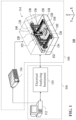
- FIG. 1 is a diagram of a near-field scanning system in accordance with an embodiment of the invention.
- FIG. 2 is a top view of an exemplary integrated transverse electromagnetic (TEM) transmission line structure with an air-dielectric coplanar waveguide (CPW) in accordance with an embodiment of the invention.
- TEM transverse electromagnetic
- FIG. 3 is a perspective view of the exemplary integrated TEM transmission line structure illustrated in FIG. 2 .
- FIG. 4 is a bottom view of the exemplary integrated TEM transmission line structure illustrated in FIG. 2 .
- FIG. 5 is a top view of the exemplary integrated TEM transmission line structure illustrated in FIG. 2 configured with connectors in accordance with an embodiment of the invention.
- FIG. 6 is a perspective view of the exemplary integrated TEM transmission line structure illustrated in FIG. 5 .
- FIG. 7 is a flow diagram of an exemplary process for forming an air-dielectric CPW in accordance with an embodiment of the invention.
- FIG. 8 is a graph of simulation results illustrating the tangential field across an exemplary air trace for various frequencies in accordance with an embodiment of the invention.
- FIG. 9 is a graph of simulation results illustrating the longitudinal field across an exemplary air trace for various frequencies in accordance with an embodiment of the invention.
- FIG. 10 is a graph of simulation results illustrating the S 11 and S 21 parameters corresponding to an exemplary air trace in accordance with an embodiment of the invention.
- FIG. 11 is a graph illustrating a comparison between simulations and measurements of an S 11 parameter corresponding to an exemplary air trace in accordance with an embodiment of the invention.
- FIG. 12 is a graph illustrating a comparison between simulations and measurements of an S 21 parameter corresponding to an exemplary air trace in accordance with an embodiment of the invention.
- FIG. 13 is a graph of measurement results illustrating magnetic field components across an exemplary air-dielectric CPW in accordance with an embodiment of the invention.
- FIG. 14 is a graph of measurement results illustrating magnetic field components across a conventional CPW in accordance with an embodiment of the invention.
- FIG. 15 is a graph illustrating a comparison of tangential fields across an exemplary air trace for various printed circuit board (PCB) thicknesses in accordance with an embodiment of the invention.
- FIG. 16 is a graph illustrating a comparison S 21 parameters corresponding to an exemplary air trace for various PCB thicknesses in accordance with an embodiment of the invention.
- a transmission line for probe calibration that includes an air-dielectric coplanar waveguide (CPW).
- CPW air-dielectric coplanar waveguide
- TEM transverse electromagnetic
- the air-dielectric CPW design disclosed herein is particularly desirable for high frequency probe calibration since it provides a more pure TEM structure relative to TEM structures that utilize a conventional CPW.
- TEM transverse electromagnetic
- EMI electromagnetic interference
- ESD electrostatic discharge
- CSP current spreading
- PPM phase measurement
- ESM emission source microscopy
- the near-field scanning system 100 includes a transverse electromagnetic (TEM) transmission line structure 102 configured to calibrate near-field probes used to measure an equipment under test (EUT), which can be an integrated circuit (IC), a printed circuit board (PCB) or any electronic device, module or system, in accordance with an embodiment of the invention is described.
- EUT equipment under test
- EMC electromagnetic compatibility
- the challenge in electromagnetic compatibility (EMC) analysis is often locating the source of emissions, the coupling paths, and the antennas.
- EMC electromagnetic compatibility
- the most basic coupling theory for EMI predicts a broadband or linear increase of the coupling strength with increasing frequency.
- the electrical analyzing instrument 110 is a network analyzer 110 , in particular, a vector network analyzer.
- the electrical analyzing instrument 110 is referred to herein as a network analyzer.
- the electrical analyzing instrument 110 can be one of many commercially available vector network analyzers.
- the electrical analyzing instrument 110 may be a spectrum analyzer with a tracking generator or a spectrum analyzer with a radio frequency (RF) generator, or an RF source and an oscilloscope.
- RF radio frequency
- the motor driver 116 of the automatic scanning subsystem 106 is designed to provide driving signals to the probe positioning mechanism 114 so that the probe 108 can be displaced to desired testing locations of the EUT and/or be rotated to desired rotational positions.
- the motor driver 116 is electrically connected to the motors 130 and 132 of the probe positioning mechanism 114 to provide driving signals to these motors so that the probe 108 can be linearly displaced along the X-axis and the Y-axis.
- the motor driver 116 is also electrically connected to the motors 138 and 140 of the scan head 122 to provide driving signals to these motors so that the probe 108 can be vertically moved along the Z-axis and be rotated about the Z-axis.
- the motor driver 116 is controlled by the processing device 112 .
- the processing device 112 is able to track the movements of the probe 108 that is being displaced by the automatic scanning subsystem 106 .
- an integrated TEM transmission line structure comprises an air-dielectric coplanar waveguide (CPW) 200 formed on a printed circuit board (PCB) 280 , wherein the air-dielectric CPW 200 may include an air trace 210 in a cutout slot of the PCB 280 .
- PCB printed circuit board
- the TEM transmission line structure may further include a first grounded CPW (GCPW) 260 on a first end of the air-dielectric CPW 200 , wherein the first GCPW 260 includes a first trace 220 aligned with the air trace 210 , and a second GCPW 270 on a second end of the air-dielectric CPW 200 , wherein the second grounded CPW 270 includes a second trace 230 aligned with the air trace 210 .
- the air-dielectric CPW 200 may comprise an air trace 210 in a cutout slot of the PCB 280 .
- the first trace 220 and second trace 230 may also include a corresponding set of vias, 222 and 232 , respectively, as shown.
- the air trace 210 is plated (e.g., a copper plating) except on each of a first end of the cutout slot and a second end of the cutout slot.
- each of the first end of the cutout slot and the second end of the cutout slot are un-plated (i.e., un-plated end 212 and un-plated end 214 , respectively).
- plat e.g., edge-plating
- PCB printed circuit board
- the impedance of the air-dielectric CPW 200 is matched with the impedance of the first GCPW 260 and/or second GCPW 270 .
- at least one connector may be electrically coupled to either the first GCPW 260 or the second GCPW 270 (See e.g., FIGS.
- the impedance of the at least one connector may be matched with the impedance of the first GCPW 260 and/or second GCPW 270 (i.e., to avoid reflections caused by the transition from the connector to the first GCPW 260 and/or second GCPW 270 ).
- connectors may be electrically coupled directly to a first and opposite end of the air-dielectric CPW 200 (i.e., a structure without the first GCPW 260 or the second GCPW 270 ), wherein the impedance of the connectors may be matched with the impedance of the air-dielectric CPW 200 .
- the dimensions of the integrated TEM transmission line structure are carefully selected so as to facilitate near-pure TEM behavior. For instance, dimensions may be selected to facilitate maintaining one of an electric near-field or a magnetic near-field having an orthogonal component across the air trace 210 and a minimized longitudinal component across the air trace 210 . Similarly, the dimensions may be selected to facilitate maintaining one of an electric near-field or a magnetic near-field having an amplitude along a line across the first and second GCPWs, 260 and 270 , wherein the dimensions further facilitate minimizing a frequency dependence of the amplitude.
- a TEM transmission line structure may comprise an air-dielectric CPW 300 formed on a PCB 380 , wherein the air-dielectric CPW 300 may include an air trace 310 in a cutout slot of the PCB 380 .
- the TEM transmission line structure may further include a first GCPW 360 on a first end of the air-dielectric CPW 300 , wherein the first GCPW 360 includes a first trace 320 aligned with the air trace 310 , and a second GCPW 370 on a second end of the air-dielectric CPW 300 , wherein the second GCPW 370 includes a second trace 330 aligned with the air trace 310 .
- the first trace 320 and second trace 330 may also include a corresponding set of vias, 322 and 332 , respectively, as shown.
- the system may also include a first connector 340 electrically coupled to the first GCPW 360 , and a second connector 350 electrically coupled to the second GCPW 370 .
- the first and second GCPWs, 360 and 370 are not plated, whereas the air trace 310 may or may not be plated.
- the air trace 310 is plated (e.g., a copper plating) except on each of a first end of the cutout slot and a second end of the cutout slot.
- each of the first end of the cutout slot and the second end of the cutout slot are un-plated (i.e., un-plated end 312 and un-plated end 314 , respectively).
- the dimensions of the integrated TEM transmission line structure are again carefully selected so as to facilitate near-pure TEM behavior. For instance, to avoid reflections caused by the transition from the air-dielectric CPW 300 to the first and second GCPWs, 360 and 370 , dimensions may be selected to facilitate an impedance match of the air-dielectric CPW 300 and the first and second GCPWs, 360 and 370 .
- the dimensions may be selected to facilitate an impedance match of the first connector 340 to the first GCPW 360 , and an impedance match of the second connector 350 to the second GCPW 370 .
- the dimensions of the TEM transmission line structure are carefully selected so as to facilitate maintaining one of an electric near-field or a magnetic near-field having an orthogonal component across the air trace 310 and a minimized longitudinal component across the air trace 310 .
- the dimensions may be selected to facilitate maintaining one of an electric near-field or a magnetic near-field having an amplitude along a line across the first and second GCPWs, 360 and 370 , wherein the dimensions further facilitate minimizing a frequency dependence of the amplitude.
- FIG. 7 a flow chart is provided, which illustrates an exemplary process for forming a TEM transmission line structure with an air-dielectric CPW in accordance with some aspects of the disclosure.
- some or all illustrated features may be omitted in a particular implementation within the scope of the present disclosure, and some illustrated features may not be required for implementation of all embodiments.
- the process 700 may be carried out by any suitable apparatus or means for carrying out the functions or algorithm described below.
- Process 700 begins at block 710 with the forming of a PCB (e.g., PCB 280 ), and concludes with the forming of an air-dielectric CPW (e.g., air-dielectric CPW 200 ) on the PCB at block 720 , wherein the air-dielectric CPW includes an air trace (e.g., air trace 210 ) formed in a cutout slot of the PCB.
- a PCB e.g., PCB 280
- an air-dielectric CPW e.g., air-dielectric CPW 200
- process 700 may further comprise forming a first GCPW (e.g., first GCPW 260 ) on a first end of the air-dielectric CPW, wherein the first GCPW includes a first trace (e.g., first trace 220 ) aligned with the air trace, and forming a second GCPW (e.g., second GCPW 270 ) on a second end of the air-dielectric CPW, wherein the second GCPW includes a second trace (e.g., second trace 230 ) aligned with the air trace.
- a first GCPW e.g., first GCPW 260
- first trace e.g., first trace 220
- second GCPW e.g., second GCPW 270
- process 700 may further comprise plating the air trace (e.g., a copper plating). Within such embodiment, it is contemplated that process 700 may further comprise the removal of each of a first plating and a second plating from each of a first end of the cutout slot (e.g., un-plated end 212 ) and a second end of the cutout slot (e.g., un-plated end 214 ).
- plating the air trace e.g., a copper plating
- process 700 may further comprise the removal of each of a first plating and a second plating from each of a first end of the cutout slot (e.g., un-plated end 212 ) and a second end of the cutout slot (e.g., un-plated end 214 ).
- process 700 may further comprise matching the impedance of the air-dielectric CPW with the impedance of the first and second GCPWs.
- process 700 may also comprise electrically coupling a connector to either end of the air-dielectric CPW (e.g., either directly to either end of the air-dielectric CPW, or via the first and second GCPWs)
- process 700 may further comprise matching the impedance of the connectors with the impedance of the air-dielectric CPW (i.e., to avoid reflections caused by a transition from the connector to the air-dielectric CPW, if the connectors are directly connected to the air-dielectric CPW), and/or matching the impedance of the connectors with the impedance of the first and second GCPWs (i.e., to avoid reflections caused by a transition from the connector to the first or second GCPW, if the connectors are connected to the air-dielectric CPW via the first and second GCPWs).
- process 700 may comprise selecting the dimensions of the integrated TEM transmission line structure so as to facilitate near-pure TEM behavior.
- the selecting of dimensions may facilitate maintaining one of an electric near-field or a magnetic near-field having an orthogonal component across the air trace and a minimized longitudinal component across the air trace.
- the selecting of dimensions may facilitate maintaining one of an electric near-field or a magnetic near-field having an amplitude along a line across the first and second GCPWs to further facilitate minimizing a frequency dependence of the amplitude.
- a 2.4 millimeter (mm) connector (e.g., first connector 340 and/or second connector 350 ) is attached to a 1 mm thick PCB (e.g., PCB 380 ) with a 1 mm wide trace (e.g., first trace 320 and/or second trace 330 ).
- the trace (e.g., first trace 320 and/or second trace 330 ) continues in an air trace (e.g., air trace 310 ) formed by a cutout slot in the PCB, which may be plated with copper.
- a transmission line with a characteristic impedance of 50 ⁇ with low loss and almost pure TEM may be obtained.
- the structure disclosed herein can be PCB-manufactured, which desirably avoids the possibility of human error associated with man-made craftsmanship.
- the cutout slot may be completely plated, which would cause the trace to be short circuited to ground.
- aspects disclosed herein contemplate removing (e.g., drilling away) the plating at the ends of the cutout slot (e.g., forming un-plated end 312 and un-plated end 314 ).
- the calibration structure for this particular implementation was evaluated with respect to the longitudinal field component (non-TEM mode), S-parameters, and amplitude across and along the air trace.
- Time domain reflectometry (TDR) was used in measurements to analyze imperfections in the structure.
- the near-field was evaluated 1 mm above the transmission line, which is a typical scanning height for high frequency (up to EHF band of radio frequencies) applications.
- TDR Time domain reflectometry
- FIGS. 8 - 9 simulation results are provided respectively illustrating the orthogonal and longitudinal fields across the air trace for various frequencies.
- the air-dielectric CPW yields desirable results up to 30 GHz.
- Orthogonal fields across the air trace are frequency-independent up to the EHF band of radio frequencies, and the longitudinal field is negligible.
- simulation results are provided illustrating the S 11 and S 21 parameters corresponding to the air trace. A comparison between actual measurements and the simulations were also made.
- FIGS. 11 - 12 for instance, a comparison between simulations and measurements for each of an S 11 and S 21 parameter corresponding to the air trace are respectively provided. As illustrated, although there are differences in amplitude, there is desirable agreement with trends.
- FIG. 13 is a graph of measurement results illustrating magnetic field components across the air trace
- FIG. 14 illustrates measurements of magnetic field components across the grounded CPW.
- the H-field across a 0.762 mm GCPW is compared with the same field of a 1 mm thick air-dielectric CPW at 30 GHz.
- the H y (tangential component) of the air-dielectric CPW is negligible compared to the orthogonal fields (H x and H z ) at all points across the air-dielectric CPW.
- the measurements and simulations of the air-dielectric CPW disclosed herein reveal that the transition between the GCPW and the air-dielectric CPW should be accounted for in order to avoid standing waves and loss.
- the wavelength in free space is 7.5 mm.
- the PCB thickness can be made thinner.
- the PCB may be designed with 0.8 mm and 0.6 mm thicknesses, and the air and substrate gaps may be adjusted to the thinner board in order to obtain a 50 ⁇ characteristic impedance.
- FIG. 15 provides a comparison of orthogonal fields across the air-dielectric CPW for various PCB thicknesses
- FIG. 16 provides a comparison of S 21 parameters corresponding to the air-dielectric CPW for various PCB thicknesses.
- both standing waves and loss are reduced with thinner boards.
- the variation along the air-dielectric CPW at 30 GHz is reduced to approximately 3 dB for the 0.6 mm board corresponding to the reflections caused by the transition from the connectors (e.g., first connector 340 and/or second connector 350 ) to the GCPWs.
- Attenuators can be included along the transmission line.
- first connector 340 to first GCPW 360 , and first GCPW 360 to air trace 310 and on the opposite end, second connector 350 to second GCPW 370 , and second GCPW 370 to air trace 310 .
- four attenuators might be needed, which may cause an undesirably large reduction in the dynamic range.
Abstract
Description
where ref is the normalized near-field strength (E or H) from a simulation at a given input voltage and at a given height above the TL:
-
- 1) Well defined field components (i.e., the near-field should be orthogonal to the direction of propagation and there should be no longitudinal component).
- 2) The near-field amplitude along a line across the TL should be as frequency-independent as possible.
- 3) Impedance matched in order to avoid reflections. If reflections arise, the calibration probe can measure the field along the line and relate the average to the average in the simulation.
Claims (19)
Priority Applications (1)
| Application Number | Priority Date | Filing Date | Title |
|---|---|---|---|
| US16/458,004 US11631927B2 (en) | 2019-06-29 | 2019-06-29 | Probe calibration system and method for electromagnetic compatibility testing |
Applications Claiming Priority (1)
| Application Number | Priority Date | Filing Date | Title |
|---|---|---|---|
| US16/458,004 US11631927B2 (en) | 2019-06-29 | 2019-06-29 | Probe calibration system and method for electromagnetic compatibility testing |
Publications (2)
| Publication Number | Publication Date |
|---|---|
| US20200411934A1 US20200411934A1 (en) | 2020-12-31 |
| US11631927B2 true US11631927B2 (en) | 2023-04-18 |
Family
ID=74044066
Family Applications (1)
| Application Number | Title | Priority Date | Filing Date |
|---|---|---|---|
| US16/458,004 Active 2040-11-10 US11631927B2 (en) | 2019-06-29 | 2019-06-29 | Probe calibration system and method for electromagnetic compatibility testing |
Country Status (1)
| Country | Link |
|---|---|
| US (1) | US11631927B2 (en) |
Families Citing this family (2)
| Publication number | Priority date | Publication date | Assignee | Title |
|---|---|---|---|---|
| JP7138257B1 (en) | 2021-08-12 | 2022-09-15 | 日本碍子株式会社 | waveguide element |
| CN114509715B (en) * | 2022-01-25 | 2023-06-02 | 上海特斯汀电子科技有限公司 | Radio frequency probe calibrating device |
Citations (4)
| Publication number | Priority date | Publication date | Assignee | Title |
|---|---|---|---|---|
| US5920240A (en) * | 1996-06-19 | 1999-07-06 | The Regents Of The University Of California | High efficiency broadband coaxial power combiner/splitter with radial slotline cards |
| US20020180570A1 (en) * | 2000-10-26 | 2002-12-05 | The Trustees Of Princeton University | Method and apparatus for dielectric spectroscopy or biological solustions |
| US20070024515A1 (en) * | 2005-07-28 | 2007-02-01 | Seong-Youp Suh | Coplanar waveguide fed dual-band slot antenna and method of operature therefore |
| US20160018393A1 (en) * | 2014-07-17 | 2016-01-21 | Wright State University | Transmission-line-coupled microfluidic-chip technology for electromagnetic sensing of biomolecules and bioparticles |
-
2019
- 2019-06-29 US US16/458,004 patent/US11631927B2/en active Active
Patent Citations (4)
| Publication number | Priority date | Publication date | Assignee | Title |
|---|---|---|---|---|
| US5920240A (en) * | 1996-06-19 | 1999-07-06 | The Regents Of The University Of California | High efficiency broadband coaxial power combiner/splitter with radial slotline cards |
| US20020180570A1 (en) * | 2000-10-26 | 2002-12-05 | The Trustees Of Princeton University | Method and apparatus for dielectric spectroscopy or biological solustions |
| US20070024515A1 (en) * | 2005-07-28 | 2007-02-01 | Seong-Youp Suh | Coplanar waveguide fed dual-band slot antenna and method of operature therefore |
| US20160018393A1 (en) * | 2014-07-17 | 2016-01-21 | Wright State University | Transmission-line-coupled microfluidic-chip technology for electromagnetic sensing of biomolecules and bioparticles |
Also Published As
| Publication number | Publication date |
|---|---|
| US20200411934A1 (en) | 2020-12-31 |
Similar Documents
| Publication | Publication Date | Title |
|---|---|---|
| Yan et al. | A miniature ultrawideband electric field probe based on coax-thru-hole via array for near-field measurement | |
| US8143903B2 (en) | Resonance scanning system and method for testing equipment for electromagnetic resonances | |
| CN109884407B (en) | Electromagnetic shielding effectiveness measuring system and measuring method | |
| US11631927B2 (en) | Probe calibration system and method for electromagnetic compatibility testing | |
| Marathe et al. | Effect of inhomogeneous medium on fields above GCPW PCB for near-field scanning probe calibration application | |
| Lin et al. | Design and application of a mobile miniature current probe for analysing the cause of EMI noise in IC circuits | |
| Ding et al. | Near-field scanning based shielding effectiveness analysis of system in package | |
| Hu et al. | Dual-components magnetic probe for electromagnetic interference measurement | |
| Shinde et al. | Investigation of interference in a mobile phone from a DC-to-DC converter | |
| Ye et al. | High-performance inter-PCB connectors: Analysis of EMI characteristics | |
| Sorensen et al. | Design of TEM transmission line for probe calibration up to 40 GHz | |
| Wu et al. | Investigation of semi-rigid coaxial test probes as RF injection devices for immunity tests at PCB level | |
| CN109884406B (en) | High-frequency electromagnetic shielding effectiveness measuring system, measuring method and device | |
| Lakoza et al. | Measuring radiated emission levels and EMI susceptibility of protection devices based on modal filtering | |
| Vanhee et al. | Proposed methods to measure the shielding performance of PCB level enclosures | |
| Yuhui et al. | An investigation of the shielding performance of PCB-level enclosures using a reverberation chamber | |
| Wu et al. | Performance of electric near-field probes for immunity tests | |
| Huang et al. | Investigation and mitigation of radio frequency interference caused by weak grounding of USB type-C receptacle connector | |
| Sørensen et al. | Recent developments in using measured sources in computational EMC | |
| Criel et al. | Theoretical and experimental quantitative characterization of the near-fields of printed circuit board interconnection structures | |
| Merfeldas et al. | Characterization of radiated susceptibility directivity for microstrip and coplanar lines | |
| Chua et al. | Radiated emissions estimation of an integrated circuit based on measurements in GTEM cell | |
| Hariyawan et al. | Low-cost Transverse Electromagnetic (TEM) cell design for radiated emission measurement | |
| Wu et al. | Analysis of Near-Field Probing Techniques for Immunity Tests | |
| Yang | Passive harmonic generation at spring contacts |
Legal Events
| Date | Code | Title | Description |
|---|---|---|---|
| FEPP | Fee payment procedure |
Free format text: ENTITY STATUS SET TO UNDISCOUNTED (ORIGINAL EVENT CODE: BIG.); ENTITY STATUS OF PATENT OWNER: SMALL ENTITY |
|
| FEPP | Fee payment procedure |
Free format text: ENTITY STATUS SET TO SMALL (ORIGINAL EVENT CODE: SMAL); ENTITY STATUS OF PATENT OWNER: SMALL ENTITY |
|
| STPP | Information on status: patent application and granting procedure in general |
Free format text: DOCKETED NEW CASE - READY FOR EXAMINATION |
|
| STPP | Information on status: patent application and granting procedure in general |
Free format text: NON FINAL ACTION MAILED |
|
| STCB | Information on status: application discontinuation |
Free format text: ABANDONED -- FAILURE TO RESPOND TO AN OFFICE ACTION |
|
| STCC | Information on status: application revival |
Free format text: WITHDRAWN ABANDONMENT, AWAITING EXAMINER ACTION |
|
| STPP | Information on status: patent application and granting procedure in general |
Free format text: RESPONSE TO NON-FINAL OFFICE ACTION ENTERED AND FORWARDED TO EXAMINER |
|
| STPP | Information on status: patent application and granting procedure in general |
Free format text: NON FINAL ACTION MAILED |
|
| STPP | Information on status: patent application and granting procedure in general |
Free format text: RESPONSE TO NON-FINAL OFFICE ACTION ENTERED AND FORWARDED TO EXAMINER |
|
| STPP | Information on status: patent application and granting procedure in general |
Free format text: NOTICE OF ALLOWANCE MAILED -- APPLICATION RECEIVED IN OFFICE OF PUBLICATIONS |
|
| AS | Assignment |
Owner name: AMBER PRECISION INSTRUMENTS, INC., CALIFORNIA Free format text: ASSIGNMENT OF ASSIGNORS INTEREST;ASSIGNOR:KAJBAF, HAMED;REEL/FRAME:062893/0446 Effective date: 20190821 |
|
| STCF | Information on status: patent grant |
Free format text: PATENTED CASE |