US11609284B2 - Magnetic sensor - Google Patents
Magnetic sensor Download PDFInfo
- Publication number
- US11609284B2 US11609284B2 US15/069,084 US201615069084A US11609284B2 US 11609284 B2 US11609284 B2 US 11609284B2 US 201615069084 A US201615069084 A US 201615069084A US 11609284 B2 US11609284 B2 US 11609284B2
- Authority
- US
- United States
- Prior art keywords
- magnetic
- magnetic body
- magnetic field
- magnetoresistance effect
- placement surface
- Prior art date
- Legal status (The legal status is an assumption and is not a legal conclusion. Google has not performed a legal analysis and makes no representation as to the accuracy of the status listed.)
- Active, expires
Links
Images


Classifications
-
- G—PHYSICS
- G01—MEASURING; TESTING
- G01R—MEASURING ELECTRIC VARIABLES; MEASURING MAGNETIC VARIABLES
- G01R33/00—Arrangements or instruments for measuring magnetic variables
- G01R33/02—Measuring direction or magnitude of magnetic fields or magnetic flux
- G01R33/06—Measuring direction or magnitude of magnetic fields or magnetic flux using galvano-magnetic devices
- G01R33/09—Magnetoresistive devices
- G01R33/095—Magnetoresistive devices extraordinary magnetoresistance sensors
-
- G—PHYSICS
- G01—MEASURING; TESTING
- G01R—MEASURING ELECTRIC VARIABLES; MEASURING MAGNETIC VARIABLES
- G01R33/00—Arrangements or instruments for measuring magnetic variables
- G01R33/02—Measuring direction or magnitude of magnetic fields or magnetic flux
- G01R33/06—Measuring direction or magnitude of magnetic fields or magnetic flux using galvano-magnetic devices
- G01R33/09—Magnetoresistive devices
- G01R33/093—Magnetoresistive devices using multilayer structures, e.g. giant magnetoresistance sensors
-
- G—PHYSICS
- G01—MEASURING; TESTING
- G01R—MEASURING ELECTRIC VARIABLES; MEASURING MAGNETIC VARIABLES
- G01R33/00—Arrangements or instruments for measuring magnetic variables
- G01R33/0005—Geometrical arrangement of magnetic sensor elements; Apparatus combining different magnetic sensor types
Definitions
- the present invention relates to a magnetic sensor, especially a magnetic sensor utilizing a magnetoresistance effect element.
- a magnetic sensor capable of detecting the change of the magnetic field is developed as a measuring device and used in various applications such as the galvanometer, the magnetic encoder and the like.
- a magnetic sensor is disclosed in the following Patent Document 1 in which a GMR element (Giant Magneto Resistive element) is used as the element for detecting the change of the magnetic field.
- the GMR element is a kind of element in which the output resistance value changes according to the input magnetic field, and the change of the magnetic field to be detected can be measured based on the output resistance value.
- a GMR chip (the chip for detecting magnetic field) is provided in the magnetic sensor as disclosed in Patent Document 1, wherein the GMR chip utilizes the spin valve typed GMR elements (Giant Magneto Resistive element) in which the output resistance value changes depending on the direction of the input magnetic field.
- the GMR chip utilizes the spin valve typed GMR elements (Giant Magneto Resistive element) in which the output resistance value changes depending on the direction of the input magnetic field.
- each GMR element is magnetized fixedly in a specific direction in one surface so as to detect the magnetic field in the specified direction.
- four GMR elements which have already formed the bridge circuit are provided on one GMR chip. Thus, all four GMR elements are magnetized fixedly in the same direction.
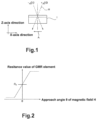
- FIG. 1 and FIG. 2 illustrate the characteristic of the GMR element.
- the GMR element is the GMR element (Giant Magneto Resistive element) made in the spin valve type in which output resistance value changes depending on the direction of the input magnetic field.
- the approach angle refers to the angle of magnetic field H relative to the GMR element.
- GMR elements are formed on the upper surface of GMR chip 1 .
- the GMR elements are arranged in such a manner that they are magnetized fixedly in the direction indicated by arrow A. Thus, the magnetic field in the direction as indicated by arrow A can be detected.
- the GMR elements are arranged in magnetic field H that enters in the direction perpendicular to the form surface of the GMR elements.
- the resistance value of the GMR element turns to “R 0 ” as shown in FIG. 2 .
- the incidence angle of magnetic field H relative to the GMR element surface deviates from the perpendicular direction with an angle of i.e., ⁇ or + ⁇ , as shown in FIG. 1 with dotted lines, wherein ⁇ (Delta) refers to the variation.
- the GMR element is magnetized fixedly in one direction and the resistance value of the GMR element changes when the direction of the magnetic field changes with respect to said direction, as shown in FIG.
- the GMR element has the following characteristic. If the resistance value is defined as R 0 when the magnetic field enters in a perpendicular direction, the resistance value will have substantial change when the direction of the magnetic field H inclines with a tiny angle.
- FIG. 3 and FIG. 4 show the configuration of the conventional magnetic sensor.
- magnetic body 21 which changes the direction of the magnetic field input to the GMR element is provided in the vicinity of the element forming part where the GMR elements in pair that are adjacent but not connected to each other in the bridge circuit are provided at almost symmetrical positions, as described in Patent Document 1.
- magnetic body 21 can change the external magnetic field in one direction into a different direction between the GMR elements.
- four GMR elements inside the bridge circuit are provided in such a manner that the magnetic field comes out in the direction in which the magnetization is fixed relative to one and comes out in the opposite direction relative to another one.
- a high differential voltage is output from the bridge circuit, and the magnetic field in one direction can be detected in precision.
- FIG. 5 is a schematic view showing the magnetic field H introduced to the GMR element parts 11 and 12 through magnetic body 21 as described in Patent Document 1.
- the magnetic field bends due to magnetic body 21 , and the component of the magnetic field is generated in the GMR element parts 11 and 12 in the direction of the induced magnetic field (magnetic field component in the X-axis direction) and the resistance value of said GMR element changes.
- the sensor is provided which is highly sensitive to the change of the magnetic field.
- the direction parallel to that where the GMR element is magnetized fixedly is defined as the X-axis direction
- the direction which is perpendicular to that where the GMR element is magnetized fixedly and also is located on the surface where the GMR elements are formed is defined as the Y-axis direction
- the direction perpendicular to the surface where the GMR elements are formed is defined as the Z-axis direction.
- FIG. 6 is a view showing the surface involving the X-axis and the Y-axis in Patent Document 1, wherein said surface is taken from the schematic view showing magnetic field H introduced to GMR elements 11 and 12 through magnetic body 21 .
- Magnetic field G is introduced from the external side of the view as shown in FIG. 6 to the internal side and is then bended with the effect from magnetic body 21 towards the direction where the magnetic induction occurs in GMR elements 11 and 12 .
- the component of the magnetic field introduced in the direction where the magnetic induction occurs in GMR elements 11 and 12 (the magnetic field in the X-axis direction) is increased, and the resistance values of the GMR elements change as mentioned above.
- Patent Document 2 has disclosed a sensor in which several magnetic bodies are provided for the magnetoresistance effect element to convert the external magnetic field in the vertical direction into magnetic field component in the horizontal direction so that the component of the magnetic field entering in the vertical direction is detected.
- Patent Document 1 JP-P5500785
- Patent Document 2 JP-P5597206
- the objective of the present invention is to solve the technical problem mentioned above. That is, the present invention aims to improve the detection precision of the magnetic sensor with an easy and convenient configuration.
- the magnetic sensor according to one embodiment of the present invention, wherein a magnetic body which changes the direction of a magnetic field input to a magnetoresistance effect element is provided in the vicinity of the magnetoresistance effect element in which the resistance value changes according to the direction of the input magnetic field, and the magnetic body has at least one chamfer part where the corner part is chamfered in the cross-section shape on the surface parallel to the placement surface of the magnetoresistance effect element.
- the magnetic field to be detected is introduced to the magnetoresistance effect element efficiently to improve the detection precision.
- the magnetic body is chamfered with a shape having at least one flat surface.
- the magnetic field to be detected can be introduced to the magnetoresistance effect element efficiently so as to improve the detection precision.
- the magnetic body is chamfered with a shape having at least one curved part.
- the magnetic field to be detected can be introduced to the magnetoresistance effect element efficiently so as to improve the detection precision.
- the magnetic body is preferably the soft magnetic body.
- the detection precision of the magnetic sensor can be improved by introducing the magnetic field to be detected to the magnetoresistance effect element through the chamfer part of the magnetic body.
- FIG. 1 is a view showing the configuration of the GMR chip.
- FIG. 2 is a diagram showing the characteristic of the GMR element.
- FIG. 3 is a view showing the configuration of the conventional magnetic sensor (the surface involving X-Z axis).
- FIG. 4 is a view showing the configuration of the conventional magnetic sensor (the surface involving X-Y axis).
- FIG. 5 is a schematic view showing the magnetic flux introduced to the GMR element part in the example of prior art (on the surface involving X-Z axis).
- FIG. 6 is a schematic view showing the magnetic flux introduced to the GMR element part in the example of prior art (on the surface involving X-Y axis).
- FIG. 7 is a view showing the configuration of the magnetic sensor in Embodiment 1 (on the surface involving X-Z axis).
- FIG. 8 is a view showing the configuration of the magnetic sensor in Embodiment 1 (on the surface involving X-Y axis).
- FIG. 9 is a schematic view showing the magnetic flux introduced to the GMR element part in Embodiment 1.
- FIG. 10 shows the stimulation results in the example of prior art and Embodiment 1 about the intensity of the magnetic field at the magnetoresistance effect element part in the X-axis direction.
- FIG. 11 is a view showing the configuration of the magnetic sensor in Embodiment 2 (on the surface involving X-Z axis).
- FIG. 12 is a view showing the configuration of the magnetic sensor in Embodiment 2 (on the surface involving X-Y axis).
- FIG. 13 is a schematic view showing the magnetic flux introduced to the GMR element part in Embodiment 2.
- FIG. 14 shows the stimulation results in the example of prior art and Embodiment 2 about the intensity of the magnetic field at the magnetoresistance effect element part in the X-axis direction.
- FIG. 15 is a view showing the configuration of the magnetic sensor in Embodiment 3 (on the surface involving X-Z axis).
- FIG. 16 is a view showing the configuration of the magnetic sensor in Embodiment 3 (on the surface involving X-Y axis).
- FIG. 17 is a schematic view showing the magnetic flux introduced to the GMR element part in Embodiment 3.
- FIG. 18 shows the stimulation results in the example of prior art and Embodiment 3 about the intensity of the magnetic field at the magnetoresistance effect element part in the X-axis direction.
- FIG. 19 is a view showing the configuration of the magnetic sensor in Embodiment 4 (on the surface involving X-Z axis).
- FIG. 20 is a view showing the configuration of the magnetic sensor in Embodiment 4 (on the surface involving X-Y axis).
- FIG. 21 is a schematic view showing the magnetic flux introduced to the GMR element part in Embodiment 4.
- FIG. 22 shows the stimulation results in the example of prior art and Embodiment 4 about the intensity of the magnetic field at the magnetoresistance effect element part in the X-axis direction.
- the GMR element is described as an example of the magnetoresistance effect element, but the element involving the magneto-resistance effect can also be used, including the TMR element, AMR element and the like.
- FIG. 7 is a view showing the configuration of the magnetic sensor according to the present embodiment on the surface involving X-Z axis.
- FIG. 8 is a view showing the configuration of the magnetic sensor according to the present embodiment on the surface involving X-Y axis.
- FIG. 9 is a schematic view showing the magnetic field entering the GMR element part through the magnetic body in the present embodiment.
- FIG. 10 shows the stimulation results in the example of prior art and the present embodiment about the intensity of the magnetic field at the magnetoresistance effect element part in the X-axis direction.
- GMR elements 111 and 112 are formed in GMR chip 110 . Further, these GMR elements form a bridge circuit. In the vicinity of the bridge circuit, magnetic body 121 changing the direction of the magnetic field input to the magnetoresistance effect element is disposed. In addition, on the cross-section involving X-Y axis, chamfer part 131 is disposed on the corner part of magnetic body 121 .
- chamfer part 131 of magnetic body 121 preferably has one flat surface.
- Magnetic body 121 is the soft magnetic body made of the material such as the ferrite material, the permalloy (Ni—Fe alloy), Sendust (Fe—Si—Al alloy) or the like.
- the material is not restricted as long as magnetic body 121 functions to change the direction of magnetic field H.
- magnetic body 121 is preferably composed of one component. However, as long as magnetic body 121 is capable of changing the direction of magnetic field H, the number of the components to constitute magnetic body 121 is not particularly restricted.
- magnetic field H introduced to GMR element parts 111 and 112 through the configuration mentioned above will be described with reference to FIG. 9 . Similar to that in the example of prior art, the magnetic field entering magnetic body 121 from the front external side of the figure in Z-axis direction is bended by magnetic body 121 and is introduced into the interior of magnetic body 121 .
- Magnetic field H introduced into the interior of magnetic body 121 is guided towards the GMR element disposing side by the chamfer shape in the vicinity of chamfer part 131 of magnetic body 121 and is then bended towards the direction where the magnetic induction occurs in the GMR element.
- the component of magnetic field H in the X-axis direction is increased to improve the detection precision of the magnetic sensor, wherein the magnetic induction occurs in the X-axis direction in the GMR element.
- the detection precision of the magnetic sensor can be improved by increasing the intensity of the magnetic field at the GMR element part.
- FIG. 11 is a view showing the configuration of the magnetic sensor according to the present embodiment on the surface involving X-Z axis.
- FIG. 12 is a view showing the configuration of the magnetic sensor according to the present embodiment on the surface involving X-Y axis.
- FIG. 13 is a schematic view showing the magnetic field entering the GMR element part through the magnetic body in the present embodiment.
- FIG. 14 shows the stimulation results in the example of prior art and the present embodiment about the intensity of the magnetic field at the magnetoresistance effect element part in the X-axis direction.
- GMR elements 211 and 212 are formed in GMR chip 210 . Further, these GMR elements form a bridge circuit. In the vicinity of the bridge circuit, magnetic body 221 changing the direction of the magnetic field input to the magnetoresistance effect element is disposed. In addition, on the cross-section involving X-Y axis, chamfer part 231 is disposed on the corner part of magnetic body 221 .
- the shape of chamfer part 231 of magnetic body 221 preferably has two flat surfaces.
- the shape of chamfer part 231 may have two or more flat surfaces as long as chamfer part 231 functions to change the direction of magnetic field H.
- Magnetic body 221 is the soft magnetic body made of the material such as the ferrite material, the permalloy (Ni—Fe alloy), Sendust (Fe—Si—Al alloy) or the like.
- the material is not restricted as long as magnetic body 221 functions to change the direction of magnetic field H.
- magnetic body 221 is preferably composed of one component. However, as long as magnetic body 221 is capable of changing the direction of magnetic field H, the number of the components to constitute magnetic body 221 is not particularly restricted.
- magnetic field H introduced to GMR element parts 211 and 212 through the configuration mentioned above will be described with reference to FIG. 13 . Similar to that in the example of prior art, the magnetic field entering magnetic body 221 from the front external side of the figure in Z-axis direction is bended by magnetic body 221 and is introduced into the interior of magnetic body 221 .
- Magnetic field H introduced into the interior of magnetic body 221 is guided towards the GMR element disposing side by the chamfer shape in the vicinity of chamfer part 231 of magnetic body 221 and is then bended towards the direction where the magnetic induction occurs in the GMR element.
- the component of magnetic field H in the X-axis direction is increased to improve the detection precision of the magnetic sensor, wherein the magnetic induction occurs in the X-axis direction in the GMR element.
- the detection precision of the magnetic sensor can be improved by increasing the intensity of the magnetic field at the GMR element part.
- FIG. 15 is a view showing the configuration of the magnetic sensor according to the present embodiment on the surface involving X-Z axis.
- FIG. 16 is a view showing the configuration of the magnetic sensor according to the present embodiment on the surface involving X-Y axis.
- FIG. 17 is a schematic view showing the magnetic field entering the GMR element part through the magnetic body in the present embodiment.
- FIG. 18 shows the stimulation results in the example of prior art and the present embodiment about the intensity of the magnetic field at the magnetoresistance effect element part in the X-axis direction.
- GMR elements 311 and 312 are formed in GMR chip 310 . Further, these GMR elements form a bridge circuit. In the vicinity of the bridge circuit, magnetic body 321 changing the direction of the magnetic field input to the magnetoresistance effect element is disposed. In addition, on the cross-section involving X-Y axis, chamfer part 331 is disposed on the corner part of magnetic body 321 .
- chamfer part 331 of magnetic body 321 preferably has an arc like shape bulging towards the center direction of magnetic body 321 .
- the arc like shape can be used for part or all of chamfer parts 331 as long as chamfer part 331 functions to change the direction of magnetic field H.
- the arc like shape and the polygon like shape can be used in combination for chamfer part 331 .
- Magnetic body 321 is the soft magnetic body made of the material such as the ferrite material, the permalloy (Ni—Fe alloy), Sendust (Fe—Si—Al alloy) or the like.
- the material is not restricted as long as magnetic body 221 functions to change the direction of magnetic field H.
- magnetic body 321 is preferably composed of one component. However, as long as magnetic body 321 is capable of changing the direction of magnetic field H, the number of the components to constitute magnetic body 321 is not particularly restricted.
- magnetic field H introduced to GMR element parts 311 and 312 through the configuration mentioned above will be described with reference to FIG. 17 .
- the magnetic field entering magnetic body 321 from the front external side of the figure in Z-axis direction is bended by magnetic body 321 and is introduced into the interior of magnetic body 321 .
- Magnetic field H introduced into the interior of magnetic body 321 is guided towards the GMR element disposing side by the chamfer shape in the vicinity of chamfer part 331 of magnetic body 321 and is then bended towards the direction where the magnetic induction occurs in the GMR element.
- the component of magnetic field H in the X-axis direction is increased to improve the detection precision of the magnetic sensor, wherein the magnetic induction occurs in the X-axis direction in the GMR element.
- the detection precision of the magnetic sensor can be improved by increasing the intensity of the magnetic field at the GMR element part.
- FIG. 19 is a view showing the configuration of the magnetic sensor according to the present embodiment on the surface involving X-Z axis.
- FIG. 20 is a view showing the configuration of the magnetic sensor according to the present embodiment on the surface involving X-Y axis.
- FIG. 21 is a schematic view showing the magnetic field entering the GMR element part through the magnetic body in the present embodiment.
- FIG. 22 shows the stimulation results in the example of prior art and the present embodiment about the intensity of the magnetic field at the magnetoresistance effect element part in the X-axis direction.
- GMR elements 411 and 412 arc formed in GMR chip 410 . Further, these GMR elements form a bridge circuit in the vicinity of the bridge circuit, magnetic body 421 changing the direction of the magnetic field input to the magnetoresistance effect element is disposed. In addition, on the cross-section involving X-Y axis, chamfer part 431 is disposed on the corner part of magnetic body 421 .
- chamfer part 431 of magnetic body 421 preferably has an arc like shape bulging towards the outside direction of magnetic body 421 .
- the arc like shape can be used for part or all of chamfer parts 431 as long as chamfer part 431 functions to change the direction of magnetic field H.
- the arc like shape and the polygon like shape can be used in combination for chamfer part 431 .
- Magnetic body 421 is the soft magnetic body made of the material such as the ferrite material, the permalloy (Ni—Fe alloy), Sendust (Fe—Si—Al alloy) or the like.
- the material is not restricted as long as magnetic body 221 functions to change the direction of magnetic field H.
- magnetic body 421 is preferably composed of one component. However, as long as magnetic body 421 is capable of changing the direction of magnetic field H, the number of the components to constitute magnetic body 421 is not particularly restricted.
- magnetic field H introduced to GMR element parts 411 and 412 through the configuration mentioned above will be described with reference to FIG. 21 . Similar to that in the example of prior art, the magnetic field entering magnetic body 421 from the front external side of the figure in Z-axis direction is bended by magnetic body 421 and is introduced into the interior of magnetic body 421 .
- Magnetic field H introduced into the interior of magnetic body 421 is guided towards the GMR element disposing side by the chamfer shape in the vicinity of chamfer part 431 of magnetic body 421 and is then bended towards the direction where the magnetic induction occurs in the GMR element.
- the component of magnetic field H in the X-axis direction is increased to improve the detection precision of the magnetic sensor, wherein the magnetic induction occurs in the X-axis direction in the GMR element.
- the detection precision of the magnetic sensor can be improved by increasing the intensity of the magnetic field at the GMR element part.
- the present invention can be applied to various measuring devices such as the magnetic sensor, the galvanometer and the encoder.
- the present invention can be utilized in the industry.
Abstract
Description
- 1 GMR chip
- 10 GMR chip in example of prior art
- 11, 12 element disposing part in example of prior art
- 21 magnetic body in example of prior art
- 110 GMR chip in
Embodiment 1 - 111, 112 element disposing part in
Embodiment 1 - 121 magnetic body in
Embodiment 1 - 131 chamfer part of magnetic body in
Embodiment 1 - 210 GMR chip in
Embodiment 2 - 211, 212 element disposing part in
Embodiment 2 - 221 magnetic body in
Embodiment 2 - 231 chamfer part of magnetic body in
Embodiment 2 - 310 GMR chip in
Embodiment 3 - 311, 312 element disposing part in
Embodiment 3 - 321 magnetic body in
Embodiment 3 - 331 chamfer part of magnetic body in
Embodiment 3 - 410 GMR chip in
Embodiment 4 - 411, 412 element disposing part in
Embodiment 4 - 421 magnetic body in
Embodiment 4 - 431 chamfer part of magnetic body in
Embodiment 4 - A fixed direction of magnetization
- H magnetic field
Claims (14)
Applications Claiming Priority (3)
| Application Number | Priority Date | Filing Date | Title |
|---|---|---|---|
| JPJP2015-049730 | 2015-03-12 | ||
| JP2015049730A JP6503802B2 (en) | 2015-03-12 | 2015-03-12 | Magnetic sensor |
| JP2015-049730 | 2015-03-12 |
Publications (2)
| Publication Number | Publication Date |
|---|---|
| US20160266218A1 US20160266218A1 (en) | 2016-09-15 |
| US11609284B2 true US11609284B2 (en) | 2023-03-21 |
Family
ID=56887815
Family Applications (1)
| Application Number | Title | Priority Date | Filing Date |
|---|---|---|---|
| US15/069,084 Active 2036-11-03 US11609284B2 (en) | 2015-03-12 | 2016-03-14 | Magnetic sensor |
Country Status (3)
| Country | Link |
|---|---|
| US (1) | US11609284B2 (en) |
| JP (1) | JP6503802B2 (en) |
| CN (1) | CN105974338B (en) |
Families Citing this family (7)
| Publication number | Priority date | Publication date | Assignee | Title |
|---|---|---|---|---|
| JP6544374B2 (en) * | 2017-03-24 | 2019-07-17 | Tdk株式会社 | Magnetic sensor |
| JP6828676B2 (en) | 2017-12-27 | 2021-02-10 | Tdk株式会社 | Magnetic sensor |
| JP6605570B2 (en) * | 2017-12-27 | 2019-11-13 | Tdk株式会社 | Magnetic sensor |
| JP7192227B2 (en) * | 2018-03-19 | 2022-12-20 | Tdk株式会社 | magnetic sensor |
| JP6620834B2 (en) * | 2018-03-27 | 2019-12-18 | Tdk株式会社 | Magnetic sensor and magnetic sensor system |
| JP2020071095A (en) * | 2018-10-30 | 2020-05-07 | Tdk株式会社 | Magnetic sensor |
| JP2020071096A (en) * | 2018-10-30 | 2020-05-07 | Tdk株式会社 | Magnetic sensor |
Citations (10)
| Publication number | Priority date | Publication date | Assignee | Title |
|---|---|---|---|---|
| US6014023A (en) * | 1997-02-26 | 2000-01-11 | Mitsubishi Denki Kabushiki Kaisha | High resolution magnetoresistance sensing device with accurate placement of inducing and detecting elements |
| WO2008146809A1 (en) | 2007-05-28 | 2008-12-04 | Mitsubishi Electric Corporation | Magnetic field detection device |
| US20090322325A1 (en) * | 2007-05-30 | 2009-12-31 | Udo Ausserlechner | Magnetic-Field Sensor |
| US20120313631A1 (en) * | 2011-06-09 | 2012-12-13 | James William Sterling | Angle measurement system including magnet with substantially square face for through-shaft applications |
| WO2013118498A1 (en) | 2012-02-07 | 2013-08-15 | 旭化成エレクトロニクス株式会社 | Magnetic sensor and magnetic detection method thereof |
| JP5500785B2 (en) | 2008-05-14 | 2014-05-21 | 新科實業有限公司 | Magnetic sensor |
| JP5597206B2 (en) | 2009-12-02 | 2014-10-01 | アルプス電気株式会社 | Magnetic sensor |
| US20150177286A1 (en) * | 2013-12-25 | 2015-06-25 | Kabushiki Kaisha Toshiba | Current sensor, current measuring module, and smart meter |
| US20150345990A1 (en) * | 2014-05-27 | 2015-12-03 | Allegro Microsystems, Llc | Systems and Methods for a Magnet with Uniform Magnetic Flux |
| US9983273B2 (en) * | 2014-05-15 | 2018-05-29 | Tdk Corporation | Magnetic field detecting sensor and magnetic field detecting apparatus using the same |
Family Cites Families (6)
| Publication number | Priority date | Publication date | Assignee | Title |
|---|---|---|---|---|
| EP2088397A4 (en) * | 2006-10-26 | 2011-06-08 | Furukawa Electric Co Ltd | Rotation angle detector |
| JP5066576B2 (en) * | 2007-10-11 | 2012-11-07 | アルプス電気株式会社 | Magnetic detector |
| US9274180B2 (en) * | 2013-07-29 | 2016-03-01 | Innovative Mion Technology | Microfabricated magnetic field transducer with flux guide |
| JP6460372B2 (en) * | 2014-06-04 | 2019-01-30 | Tdk株式会社 | Magnetic sensor, method for manufacturing the same, and measuring instrument using the same |
| JP6597369B2 (en) * | 2015-03-12 | 2019-10-30 | Tdk株式会社 | Magnetic sensor |
| JP6597370B2 (en) * | 2015-03-12 | 2019-10-30 | Tdk株式会社 | Magnetic sensor |
-
2015
- 2015-03-12 JP JP2015049730A patent/JP6503802B2/en active Active
-
2016
- 2016-03-11 CN CN201610139634.4A patent/CN105974338B/en active Active
- 2016-03-14 US US15/069,084 patent/US11609284B2/en active Active
Patent Citations (12)
| Publication number | Priority date | Publication date | Assignee | Title |
|---|---|---|---|---|
| US6014023A (en) * | 1997-02-26 | 2000-01-11 | Mitsubishi Denki Kabushiki Kaisha | High resolution magnetoresistance sensing device with accurate placement of inducing and detecting elements |
| WO2008146809A1 (en) | 2007-05-28 | 2008-12-04 | Mitsubishi Electric Corporation | Magnetic field detection device |
| US20100156405A1 (en) | 2007-05-28 | 2010-06-24 | Mitsubishi Electric Corporation | Magnetic field detection device |
| US20090322325A1 (en) * | 2007-05-30 | 2009-12-31 | Udo Ausserlechner | Magnetic-Field Sensor |
| JP5500785B2 (en) | 2008-05-14 | 2014-05-21 | 新科實業有限公司 | Magnetic sensor |
| JP5597206B2 (en) | 2009-12-02 | 2014-10-01 | アルプス電気株式会社 | Magnetic sensor |
| US20120313631A1 (en) * | 2011-06-09 | 2012-12-13 | James William Sterling | Angle measurement system including magnet with substantially square face for through-shaft applications |
| WO2013118498A1 (en) | 2012-02-07 | 2013-08-15 | 旭化成エレクトロニクス株式会社 | Magnetic sensor and magnetic detection method thereof |
| US20140375311A1 (en) | 2012-02-07 | 2014-12-25 | Asahi Kasei Microdevices Corporation | Magnetic sensor and magnetic detecting method of the same |
| US20150177286A1 (en) * | 2013-12-25 | 2015-06-25 | Kabushiki Kaisha Toshiba | Current sensor, current measuring module, and smart meter |
| US9983273B2 (en) * | 2014-05-15 | 2018-05-29 | Tdk Corporation | Magnetic field detecting sensor and magnetic field detecting apparatus using the same |
| US20150345990A1 (en) * | 2014-05-27 | 2015-12-03 | Allegro Microsystems, Llc | Systems and Methods for a Magnet with Uniform Magnetic Flux |
Also Published As
| Publication number | Publication date |
|---|---|
| JP2016170028A (en) | 2016-09-23 |
| CN105974338B (en) | 2019-06-25 |
| US20160266218A1 (en) | 2016-09-15 |
| CN105974338A (en) | 2016-09-28 |
| JP6503802B2 (en) | 2019-04-24 |
Similar Documents
| Publication | Publication Date | Title |
|---|---|---|
| US11609284B2 (en) | Magnetic sensor | |
| JP6597369B2 (en) | Magnetic sensor | |
| US9810551B2 (en) | On-axis magnetic field angle sensors, systems and method | |
| JP6597370B2 (en) | Magnetic sensor | |
| US9766304B2 (en) | Integrated AMR magnetoresistor with a set/reset coil having a stretch positioned between a magnetoresistive strip and a concentrating region | |
| US11237229B2 (en) | Magnetic field sensing apparatus | |
| CN107976644B (en) | Magnetic field detection device | |
| JP6886222B2 (en) | Magnetic sensor | |
| JP6427588B2 (en) | Magnetic sensor | |
| CN111198341B (en) | Magnetic sensor and position detection device | |
| US11754645B2 (en) | Magnetic sensor | |
| JP7057680B2 (en) | Magnetic sensor and current sensor | |
| CN112904246B (en) | Magnetic sensor | |
| US10168395B2 (en) | Magnetic sensor | |
| US10247790B2 (en) | Magnetic sensor | |
| WO2017126373A1 (en) | Magnetic medium detection device | |
| CN109974569A (en) | Magnetic Sensor | |
| US11953568B1 (en) | Wide-range perpendicular sensitive magnetic sensor and method for manufacturing the same | |
| JP2018054477A (en) | Magnetic sensor and method for manufacturing magnetic sensor | |
| WO2010095495A1 (en) | Magnetism detection device |
Legal Events
| Date | Code | Title | Description |
|---|---|---|---|
| AS | Assignment |
Owner name: TDK CORPORATION, JAPAN Free format text: ASSIGNMENT OF ASSIGNORS INTEREST;ASSIGNOR:TANABE, KEI;REEL/FRAME:037966/0804 Effective date: 20160302 |
|
| STPP | Information on status: patent application and granting procedure in general |
Free format text: FINAL REJECTION MAILED |
|
| STPP | Information on status: patent application and granting procedure in general |
Free format text: RESPONSE AFTER FINAL ACTION FORWARDED TO EXAMINER |
|
| STPP | Information on status: patent application and granting procedure in general |
Free format text: ADVISORY ACTION MAILED |
|
| STPP | Information on status: patent application and granting procedure in general |
Free format text: DOCKETED NEW CASE - READY FOR EXAMINATION |
|
| STPP | Information on status: patent application and granting procedure in general |
Free format text: NON FINAL ACTION MAILED |
|
| STPP | Information on status: patent application and granting procedure in general |
Free format text: RESPONSE TO NON-FINAL OFFICE ACTION ENTERED AND FORWARDED TO EXAMINER |
|
| STPP | Information on status: patent application and granting procedure in general |
Free format text: FINAL REJECTION MAILED |
|
| STPP | Information on status: patent application and granting procedure in general |
Free format text: ADVISORY ACTION MAILED |
|
| STCV | Information on status: appeal procedure |
Free format text: NOTICE OF APPEAL FILED |
|
| STCV | Information on status: appeal procedure |
Free format text: NOTICE OF APPEAL FILED |
|
| STCV | Information on status: appeal procedure |
Free format text: EXAMINER'S ANSWER TO APPEAL BRIEF MAILED |
|
| STCV | Information on status: appeal procedure |
Free format text: APPEAL READY FOR REVIEW |
|
| STCV | Information on status: appeal procedure |
Free format text: ON APPEAL -- AWAITING DECISION BY THE BOARD OF APPEALS |
|
| STCV | Information on status: appeal procedure |
Free format text: BOARD OF APPEALS DECISION RENDERED |
|
| STPP | Information on status: patent application and granting procedure in general |
Free format text: NOTICE OF ALLOWANCE MAILED -- APPLICATION RECEIVED IN OFFICE OF PUBLICATIONS |
|
| STPP | Information on status: patent application and granting procedure in general |
Free format text: NOTICE OF ALLOWANCE MAILED -- APPLICATION RECEIVED IN OFFICE OF PUBLICATIONS |
|
| STPP | Information on status: patent application and granting procedure in general |
Free format text: PUBLICATIONS -- ISSUE FEE PAYMENT VERIFIED |
|
| STCF | Information on status: patent grant |
Free format text: PATENTED CASE |