US11606032B2 - Adaptive combination power supply circuit and charging architecture - Google Patents
Adaptive combination power supply circuit and charging architecture Download PDFInfo
- Publication number
- US11606032B2 US11606032B2 US16/683,913 US201916683913A US11606032B2 US 11606032 B2 US11606032 B2 US 11606032B2 US 201916683913 A US201916683913 A US 201916683913A US 11606032 B2 US11606032 B2 US 11606032B2
- Authority
- US
- United States
- Prior art keywords
- transistor
- power supply
- coupled
- supply circuit
- node
- Prior art date
- Legal status (The legal status is an assumption and is not a legal conclusion. Google has not performed a legal analysis and makes no representation as to the accuracy of the status listed.)
- Active, expires
Links
- 230000003044 adaptive effect Effects 0.000 title abstract description 53
- 230000001939 inductive effect Effects 0.000 claims abstract description 37
- 239000003990 capacitor Substances 0.000 claims description 2
- 239000004065 semiconductor Substances 0.000 claims description 2
- 238000010586 diagram Methods 0.000 description 18
- 238000000034 method Methods 0.000 description 10
- 238000007726 management method Methods 0.000 description 8
- 238000004891 communication Methods 0.000 description 6
- 230000003213 activating effect Effects 0.000 description 4
- 230000008901 benefit Effects 0.000 description 4
- 230000000903 blocking effect Effects 0.000 description 4
- 230000005669 field effect Effects 0.000 description 4
- 230000006870 function Effects 0.000 description 4
- 238000006243 chemical reaction Methods 0.000 description 3
- 238000013461 design Methods 0.000 description 3
- 238000012545 processing Methods 0.000 description 3
- 230000001105 regulatory effect Effects 0.000 description 3
- 230000001413 cellular effect Effects 0.000 description 2
- 238000012163 sequencing technique Methods 0.000 description 2
- 230000002411 adverse Effects 0.000 description 1
- 238000013459 approach Methods 0.000 description 1
- 230000005540 biological transmission Effects 0.000 description 1
- 239000004020 conductor Substances 0.000 description 1
- 230000002708 enhancing effect Effects 0.000 description 1
- 238000012986 modification Methods 0.000 description 1
- 230000004048 modification Effects 0.000 description 1
- 230000003595 spectral effect Effects 0.000 description 1
- 238000012360 testing method Methods 0.000 description 1
- 230000007704 transition Effects 0.000 description 1
Images


Classifications
-
- H—ELECTRICITY
- H02—GENERATION; CONVERSION OR DISTRIBUTION OF ELECTRIC POWER
- H02J—CIRCUIT ARRANGEMENTS OR SYSTEMS FOR SUPPLYING OR DISTRIBUTING ELECTRIC POWER; SYSTEMS FOR STORING ELECTRIC ENERGY
- H02J7/00—Circuit arrangements for charging or depolarising batteries or for supplying loads from batteries
- H02J7/007—Regulation of charging or discharging current or voltage
- H02J7/0071—Regulation of charging or discharging current or voltage with a programmable schedule
-
- H02J7/0072—
-
- H—ELECTRICITY
- H02—GENERATION; CONVERSION OR DISTRIBUTION OF ELECTRIC POWER
- H02J—CIRCUIT ARRANGEMENTS OR SYSTEMS FOR SUPPLYING OR DISTRIBUTING ELECTRIC POWER; SYSTEMS FOR STORING ELECTRIC ENERGY
- H02J7/00—Circuit arrangements for charging or depolarising batteries or for supplying loads from batteries
- H02J7/34—Parallel operation in networks using both storage and other dc sources, e.g. providing buffering
-
- H—ELECTRICITY
- H02—GENERATION; CONVERSION OR DISTRIBUTION OF ELECTRIC POWER
- H02M—APPARATUS FOR CONVERSION BETWEEN AC AND AC, BETWEEN AC AND DC, OR BETWEEN DC AND DC, AND FOR USE WITH MAINS OR SIMILAR POWER SUPPLY SYSTEMS; CONVERSION OF DC OR AC INPUT POWER INTO SURGE OUTPUT POWER; CONTROL OR REGULATION THEREOF
- H02M3/00—Conversion of dc power input into dc power output
- H02M3/02—Conversion of dc power input into dc power output without intermediate conversion into ac
- H02M3/04—Conversion of dc power input into dc power output without intermediate conversion into ac by static converters
- H02M3/06—Conversion of dc power input into dc power output without intermediate conversion into ac by static converters using resistors or capacitors, e.g. potential divider
- H02M3/07—Conversion of dc power input into dc power output without intermediate conversion into ac by static converters using resistors or capacitors, e.g. potential divider using capacitors charged and discharged alternately by semiconductor devices with control electrode, e.g. charge pumps
-
- H—ELECTRICITY
- H02—GENERATION; CONVERSION OR DISTRIBUTION OF ELECTRIC POWER
- H02M—APPARATUS FOR CONVERSION BETWEEN AC AND AC, BETWEEN AC AND DC, OR BETWEEN DC AND DC, AND FOR USE WITH MAINS OR SIMILAR POWER SUPPLY SYSTEMS; CONVERSION OF DC OR AC INPUT POWER INTO SURGE OUTPUT POWER; CONTROL OR REGULATION THEREOF
- H02M3/00—Conversion of dc power input into dc power output
- H02M3/02—Conversion of dc power input into dc power output without intermediate conversion into ac
- H02M3/04—Conversion of dc power input into dc power output without intermediate conversion into ac by static converters
- H02M3/10—Conversion of dc power input into dc power output without intermediate conversion into ac by static converters using discharge tubes with control electrode or semiconductor devices with control electrode
- H02M3/145—Conversion of dc power input into dc power output without intermediate conversion into ac by static converters using discharge tubes with control electrode or semiconductor devices with control electrode using devices of a triode or transistor type requiring continuous application of a control signal
- H02M3/155—Conversion of dc power input into dc power output without intermediate conversion into ac by static converters using discharge tubes with control electrode or semiconductor devices with control electrode using devices of a triode or transistor type requiring continuous application of a control signal using semiconductor devices only
- H02M3/156—Conversion of dc power input into dc power output without intermediate conversion into ac by static converters using discharge tubes with control electrode or semiconductor devices with control electrode using devices of a triode or transistor type requiring continuous application of a control signal using semiconductor devices only with automatic control of output voltage or current, e.g. switching regulators
- H02M3/158—Conversion of dc power input into dc power output without intermediate conversion into ac by static converters using discharge tubes with control electrode or semiconductor devices with control electrode using devices of a triode or transistor type requiring continuous application of a control signal using semiconductor devices only with automatic control of output voltage or current, e.g. switching regulators including plural semiconductor devices as final control devices for a single load
- H02M3/1582—Buck-boost converters
Definitions
- Certain aspects of the present disclosure generally relate to electronic circuits and, more particularly, to an adaptive combination power supply circuit.
- a voltage regulator ideally provides a constant direct current (DC) output voltage regardless of changes in load current or input voltage.
- Voltage regulators may be classified as linear regulators or switching regulators. While linear regulators tend to be relatively compact, many applications may benefit from the increased efficiency of a switching regulator.
- a linear regulator may be implemented by a low-dropout (LDO) regulator, for example.
- LDO low-dropout
- a switching regulator may be implemented, for example, by a switched-mode power supply (SMPS), such as a buck converter, a boost converter, a buck-boost converter, or a charge pump.
- SMPS switched-mode power supply
- a buck converter is a type of SMPS typically comprising: (1) a high-side switch coupled between a relatively higher voltage rail and a switching node, (2) a low-side switch coupled between the switching node and a relatively lower voltage rail, (3) and an inductor coupled between the switching node and a load (e.g., represented by a shunt capacitive element).
- the high-side and low-side switches are typically implemented with transistors, although the low-side switch may alternatively be implemented with a diode.
- Power management integrated circuits are used for managing the power requirement of a host system and may include and/or control one or more voltage regulators (e.g., buck converters or charge pumps).
- a PMIC may be used in battery-operated devices, such as mobile phones, tablets, laptops, wearables, etc., to control the flow and direction of electrical power in the devices.
- the PMIC may perform a variety of functions for the device such as DC-to-DC conversion, battery charging, power-source selection, voltage scaling, power sequencing, etc.
- Certain aspects of the present disclosure generally relate to an adaptive combination power supply circuit and methods for operation of such a power supply circuit.
- the power supply circuit generally includes a first transistor; a second transistor coupled to the first transistor via a first node; a third transistor coupled to the second transistor via a second node; a fourth transistor coupled to the third transistor via a third node; a capacitive element having a first terminal coupled to the first node and a second terminal coupled to the third node; an inductive element having a first terminal coupled to the second node; and a switch having a first terminal coupled to the first terminal of the inductive element, the switch having a second terminal coupled to a second terminal of the inductive element.
- Certain aspects of the present disclosure provide a power management integrated circuit (PMIC) comprising at least a portion of the power supply circuit described above.
- PMIC power management integrated circuit
- Certain aspects of the present disclosure provide a battery charging circuit comprising the power supply circuit described above.
- the battery charging circuit generally includes a master charging circuit and at least one slave charging circuit having an output coupled in parallel with an output of the master charging circuit. At least one of the master charging circuit or the slave charging circuit comprises the power supply circuit described above.
- Certain aspects of the present disclosure provide a method of regulating power.
- the method generally includes operating a power supply circuit in a first operation mode, the power supply circuit including an inductive element and a switch coupled in parallel with the inductive element, wherein the switch is open in the first operation mode; and closing the switch to operate the power supply circuit in a second operation mode.
- the first operation mode may be a three-level buck converter mode.
- the second operation mode may be a divide-by-two charge pump mode.
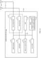
- FIG. 1 is a block diagram of an example master-slave charging circuit for charging a battery, where the master-slave charging circuit includes two parallel charging circuits.
- FIG. 2 is a block diagram of an example adaptive combination power supply circuit implemented in a master charging circuit, in accordance with certain aspects of the present disclosure.
- FIG. 3 A is an equivalent circuit diagram of the example adaptive combination power supply circuit in FIG. 2 when a transistor across an inductor is deactivated, in accordance with certain aspects of the present disclosure.
- FIG. 3 B is an equivalent circuit diagram of the example adaptive combination power supply circuit in FIG. 2 when the transistor across the inductor is activated, in accordance with certain aspects of the present disclosure.
- FIG. 4 is a block diagram of an example adaptive combination power supply circuit implemented in a slave charging circuit, in accordance with certain aspects of the present disclosure.
- FIG. 5 is a block diagram of an example parallel charging circuit in which both the master charging circuit and the slave charging circuit use an adaptive combination power supply circuit, in accordance with certain aspects of the present disclosure.
- FIG. 5 is divided across multiple sheets labeled FIG. 5 A and FIG. 5 B , this block diagram will hereinafter be referred to as FIG. 5 . The reader is to understand that portions of this block diagram may appear in FIG. 5 A , FIG. 5 B , or both.
- FIG. 6 is a block diagram of an example device comprising a power management integrated circuit (PMIC) that includes an adaptive combination power supply circuit, in accordance with certain aspects of the present disclosure.
- PMIC power management integrated circuit
- FIG. 7 is a flow diagram of example operations for regulating power, in accordance with certain aspects of the present disclosure.
- the adaptive combination power supply circuit may be capable of switching between performing as a three-level buck converter and as a divide-by-two charge pump.
- connection in the various tenses of the verb “connect” may mean that element A is directly connected to element B or that other elements may be connected between elements A and B (i.e., that element A is indirectly connected with element B).
- connection may also be used herein to mean that a wire, trace, or other electrically conductive material is used to electrically connect elements A and B (and any components electrically connected therebetween).
- a battery charging circuit may be utilized.
- the battery charging circuit or at least a portion thereof, may reside in a power management integrated circuit (PMIC) in the device.
- PMIC power management integrated circuit
- the battery charging circuit may comprise two or more parallel charging circuits, each capable of charging the battery, which may be connected together and to the battery in an effort to provide fast charging of the battery.
- the parallel charging circuits may be configured so that these circuits do not adversely interfere with each other during battery charging (e.g., in a master-slave relationship).
- Example master-slave battery charging circuits are described in U.S. Pat. No. 9,590,436 to Sporck et al., filed Apr. 11, 2014 and entitled “Master-Slave Multi-Phase Charging.”
- FIG. 1 is a block diagram of an example master-slave charging circuit 100 for charging a battery 102 .
- the master-slave charging circuit 100 includes two parallel charging circuits: a main charger 104 (also referred to as a master charger) and a parallel charger 106 (also referred to as a slave charger).
- the main charger 104 and the parallel charger 106 may receive power from the same power supply voltage rail 108 (e.g., with input voltage VIN as illustrated in FIG. 1 ) or from different power sources (e.g., different power supply rails).
- the main charger 104 and the parallel charger 106 may use the same or different power supply circuit topologies.
- the main charger 104 may employ a switched-mode power supply (SMPS) topology (e.g., a buck converter topology), while the parallel charger 106 is implemented with a charge pump topology or the same SMPS topology.
- SMPS switched-mode power supply
- the main charger 104 and the parallel charger 106 may include or be connected to an inductor L 1 and an inductor L 2 , respectively, in an effort to maintain continuous current out of the chargers and into respective loads.
- the main charger 104 may control the parallel charger 106 , but both chargers in the master-slave charging circuit 100 are utilized to charge the battery 102 from respective output voltages, coupled to a battery voltage node (VBAT).
- VBAT battery voltage node
- the main charger 104 may also be used to provide power to other loads within the device (referred to as the system load voltage, or VSYS LOAD)
- the parallel charger 106 may be used solely to charge the battery 102 .
- Battery charging systems are trending towards higher charging current, which leads to the desire for higher efficiency converters that can operate over a wider battery voltage range. To reduce thermal issues and/or conserve power, it may be desirable to operate such battery charging systems with higher efficiency.
- the master charger is implemented based on a buck converter topology.
- the master charger is capable of charging the battery and providing power by itself or may be paralleled with one or more slave chargers.
- Each of the slave chargers may be implemented as a switched-capacitor converter (e.g., a divide-by-two (Div2) charge pump) or a switched-mode power supply (SMPS) topology using an inductor (e.g., a buck converter).
- SMPS switched-mode power supply
- Charge pump converters may provide a more efficient alternative to buck converters.
- a Div2 charge pump may operate efficiently under constant current (CC) mode, but may not work efficiently under constant voltage (CV) mode. Consequently, in some applications such as battery chargers, another power supply topology (e.g., an inductor-based SMPS) may be implemented in conjunction with the charge pump. Furthermore, a Div2 charge pump may not support higher power or higher charging current with certain adaptor cables (e.g., 3 A cables).
- CC constant current
- CV constant voltage
- a Div2 charge pump may not support higher power or higher charging current with certain adaptor cables (e.g., 3 A cables).
- certain aspects of the present disclosure provide a charger architecture for further enhancing charging efficiency, especially under heavy load.
- this charger architecture further increases power density to reduce the solution size and use a smaller inductor, balances power loss, avoids a thermal hot spot, supports a higher power specification with existing adaptor cables (e.g., 3 A cables), and/or operates in the highest efficiency range in different scenarios.
- FIG. 2 is a block diagram of an example adaptive combination power supply circuit 200 implemented as a master charging circuit, in accordance with certain aspects of the present disclosure.
- the adaptive combination power supply circuit 200 may be realized by adding a switch 201 across an inductive element L 1 of a three-level buck converter topology.
- the three-level buck converter topology may include a first transistor Q 1 , a second transistor Q 2 , a third transistor Q 3 , a fourth transistor Q 4 , a flying capacitive element Cfly, the inductive element L 1 , and a load 203 , which is represented here by capacitive element C 3 .
- Transistor Q 2 may be coupled to transistor Q 1 via a first node 202
- transistor Q 3 may be coupled to transistor Q 2 via a second node 204
- transistor Q 4 may be coupled to transistor Q 3 via a third node 206 .
- the transistors Q 1 -Q 4 may be implemented as n-type metal-oxide-semiconductor (NMOS) transistors, as illustrated in FIG. 2 .
- NMOS n-type metal-oxide-semiconductor
- the drain of transistor Q 2 may be coupled to the source of transistor Q 1
- the drain of transistor Q 3 may be coupled to the source of transistor Q 2
- the drain of transistor Q 4 may be coupled to the source of transistor Q 3 .
- the source of transistor Q 4 may be coupled to a reference potential node 229 (e.g., electric ground, labeled “PGND_CHG”) for the circuit.
- the flying capacitive element Cfly may have a first terminal 208 coupled to the first node 202 and a second terminal 210 coupled to the third node 206 .
- the inductive element L 1 may have a first terminal 212 coupled to the second node 204 (also referred to as the “switching node”) and a second terminal 214 coupled to the output voltage node 215 (labeled “VPH_PWR”) and the load 203 .
- the switch 201 may be coupled in parallel with the inductive element L 1 , having a first terminal 216 coupled to the first terminal 212 of the inductive element L 1 and a second terminal 218 coupled to the second terminal 214 of the inductive element L 1 .
- the switch 201 may be implemented by a transistor, such as transistor Q 6 , which may be an NMOS transistor.
- the source of transistor Q 6 may be coupled to the first terminal 212 of the inductive element L 1
- the drain of transistor Q 6 may be coupled to the second terminal 214 of the inductive element L 1 .
- Control logic 220 may control operation of the adaptive combination power supply circuit 200 .
- the control logic 220 may control operation of transistors Q 1 -Q 4 via output signals to the inputs of respective gate drivers 221 - 224 .
- the outputs of the gate drivers 221 - 224 are coupled to respective gates of transistors Q 1 -Q 4 .
- the control logic 220 may cycle through four different phases. In a first phase, transistors Q 1 and Q 3 are activated, and transistors Q 2 and Q 4 are deactivated, to charge the flying capacitive element Cfly and to energize the inductive element L 1 .
- transistor is Q 1 is deactivated, and transistor Q 4 is activated, such that the switching node (second node 204 ) is coupled to the reference potential node (e.g., PGND_CHG), the flying capacitive element Cfly is disconnected, and the inductive element L 1 is deenergized.
- transistors Q 2 and Q 4 are activated, and transistor Q 3 is deactivated, to discharge the flying capacitive element Cfly and to energize the inductive element L 1 .
- transistor Q 3 is activated, and transistor Q 2 is deactivated, such that the flying capacitive element Cfly is disconnected and the inductive element L 1 is deenergized.
- control logic 220 has an output signal labeled “EN_Div2” configured to control operation of the switch 201 and selectively enable divide-by-two charge pump operation.
- EN_Div2 an output signal labeled “EN_Div2” configured to control operation of the switch 201 and selectively enable divide-by-two charge pump operation.
- the EN_Div2 signal when the EN_Div2 signal is logic low, the switch 201 is open, and the adaptive combination power supply circuit 200 operates as a three-level buck converter using the inductive element L 1 .
- the switch 201 is closed, thereby shorting across the inductive element L 1 and effectively removing the inductive element L 1 from the circuit, such that the power supply circuit 200 operates as a divide-by-two charge pump.
- the control logic 220 may be configured to automatically control operation of the switch 201 (e.g., through the logic level of the EN_Div2 signal) based on at least one of an input voltage (e.g., USB_IN from a Universal Serial Bus (USB) power source) or an operation mode, for the power supply circuit 200 .
- an input voltage e.g., USB_IN from a Universal Serial Bus (USB) power source
- an operation mode for the power supply circuit 200 .
- FIG. 3 A is an equivalent circuit diagram of the example adaptive combination power supply circuit 200 in FIG. 2 when transistor Q 6 across the inductive element L 1 is deactivated.
- FIG. 3 B is an equivalent circuit diagram of the example adaptive combination power supply circuit 200 in FIG. 2 when transistor Q 6 across the inductive element L 1 is activated.
- the adaptive combination power supply circuit 200 may also include a capacitive element C 1 , a reverse current blocking transistor Q 0 , a capacitive element C 2 , a transistor Q 5 , a battery 230 , and a battery capacitive element C BAT .
- the reverse current blocking transistor Q 0 (which may be referred to as a front-porch field-effect transistor (FPFET)) may be coupled between the input voltage node (USB_IN) and the drain of transistor Q 1 at node 232 (labeled “MID_CHG”).
- the capacitive element C 1 may be coupled in shunt between the input voltage node USB_IN and the reference potential node 229
- the capacitive element C 2 may be coupled in shunt between node 232 and the reference potential node 229 .
- the reverse current blocking transistor Q 0 may be implemented as an NMOS transistor, where the source of transistor Q 0 is coupled to the input voltage node USB_IN and the drain of transistor Q 0 coupled to node 232 .
- Transistor Q 5 may be referred to as a battery field-effect transistor (BATFET)), which may be implemented by an NMOS transistor as depicted.
- BATFET battery field-effect transistor
- the drain of transistor Q 5 may be coupled to the output voltage node 215 (VPH_PWR), and the source of transistor Q 5 may be coupled to a terminal of the battery (labeled “VBATT_PWR”).
- the gate of transistor Q 5 may be controlled by battery logic 234 and a gate driver 236 as shown.
- the battery capacitive element C BAT may be coupled in shunt across the terminals of the battery 230 (VBATT_PWR and the reference potential node 229 ).
- the adaptive combination power supply circuit 200 may be implemented in an integrated circuit 250 .
- at least transistors Q 0 -Q 5 , control logic 220 , gate drivers 221 - 224 , battery logic 234 , and gate driver 236 may be included in the integrated circuit 250 .
- the capacitive elements C 1 , C 2 , C 3 , and C BAT , the inductive element L 1 , and the battery 230 may be implemented outside of the integrated circuit 250 .
- the switch 201 may be fabricated as part of the integrated circuit 250 for certain aspects.
- the adaptive combination power supply circuit may be capable of switching between performing as a three-level buck converter and as a divide-by-two charge pump, by opening or closing a switch connected in parallel with the inductor.
- the transition may be adaptive depending on adaptor type, cable type, charging status, protection capability (e.g., current limit), etc.
- the adaptive combination power supply circuit may operate as a 3-level buck converter during trickle and precharging modes, operate as a Div2 charge pump during CC mode, and back to operating as a 3-level buck converter in CV mode to finish charging.
- the adaptive combination power supply circuit achieves the benefits of both a 3-level buck converter and a Div2 charge pump. Its flexible architecture offers different configuration options for different customer specifications.
- the adaptive combination power supply circuit may be configured as a 3-level buck converter, as a Div2 charge pump, or as an adaptive combination converter capable of automatically transitioning between operating as either a 3-level buck converter or a Div2 charge pump depending on operating conditions.
- the adaptive combination power supply circuit can support different adaptors at the highest efficiency and can support high power delivery with high efficiency.
- transistor Q 6 may be deactivated (the switch is opened), and the circuit operates as a 3-level buck converter to support higher power with high efficiency.
- FIG. 4 is a block diagram of an example adaptive combination power supply circuit 400 implemented as a slave charging circuit, in accordance with certain aspects of the present disclosure.
- the adaptive combination power supply circuit 400 of FIG. 4 includes capacitive elements C 4 and C 5 .
- the input voltage node 402 for the adaptive combination power supply circuit 400 may be coupled to node 232 and may receive a USB_IN voltage as illustrated.
- the output voltage node 404 (labeled “VOUT_S” for slave output voltage) may be coupled to a load 405 , which is represented here by shunt capacitive element C 5 .
- the architecture illustrated in FIG. 4 may be operated in 3-level buck converter mode, operated in a Div2 charge pump mode, or may be automatically transitioned between the 3-level buck converter and Div2 charge pump modes, depending on operation conditions.
- a reverse current blocking transistor (which may be referred to as a front-porch field-effect transistor (FPFET)) may be added between the drain of transistor Q 1 and the input voltage node 402 (USB_IN), and/or a transistor (e.g., a battery field-effect transistor (BATFET)) may be added between VOUT_S and the load (e.g., a battery), similar to the power supply circuit 200 of FIG. 2 .
- FFPFET front-porch field-effect transistor
- BATFET battery field-effect transistor
- the slave charger may be turned off (e.g., if the slave charger does not support the VPH_PWR load, typically supplied by the master charger).
- the slave charger may be turned on and may operate as a three-level buck converter or a Div2 charge pump. Under certain conditions (e.g., a particular Vin and Vout window), transistor Q 6 may be activated (the switch is closed), and Div2 charge pump operation is selected for higher efficiency.
- transistor Q 6 may be deactivated (the switch is opened), and the circuit may operate as a 3-level buck converter to support higher power with high efficiency.
- CV mode Once CV mode is entered, the slave charger may be turned off, and the master charger may be used by itself.
- FIG. 5 is a block diagram of an example parallel charging circuit 500 , in accordance with certain aspects of the present disclosure.
- the parallel charging circuit 500 includes a master charging circuit 502 (e.g., power supply circuit 200 of FIG. 2 ) and a slave charging circuit 504 (e.g., power supply circuit 400 of FIG. 4 ), in which both the master and slave charging circuits are implemented with an adaptive combination power supply circuit, as described above. While a single slave charging circuit 504 is illustrated in FIG. 5 , more than one slave charging circuit (e.g., two slave charging circuits) may be utilized to charge the battery in other parallel charging solutions.
- One or more of these multiple slave charging circuits may be implemented with adaptive combination power supply circuits, as described herein.
- Other of the multiple slave charging circuits may be implemented with a traditional topology, such as a 3-level or 2-level buck converter.
- VOUT output voltage node
- the VOUT node of the slave charging circuit 504 is illustrated in FIG. 5 as being connected to the battery pack and to the VBATT_PWR node of the master charging circuit 502 , the VOUT node of the slave charging circuit may be connected to the VPH_PWR node of the master charging circuit for other aspects.
- a single software point-of reference may be used to support different configurations (e.g., various input/output options), via the control logic.
- different configurations e.g., various input/output options
- the selection between different power supply circuits is significantly simplified, with the number of options reduced.
- the adaptive combination converter architecture can improve the efficiency by about 2-3% at loads higher than 2 A, which may represent 200 mW to 400 mW less power loss compared to conventional approaches.
- the adaptive combination charger may automatically switch to Div2 mode, for example, when one or more conditions are met.
- the adaptive combination power supply circuit When operating in Div2 mode, the adaptive combination power supply circuit will have even less power loss and higher efficiency.
- the peak efficiency of the adaptive combination circuit operating in Div2 mode with a 4 A load is about 97%, for example.
- circuits disclosed herein may be used in many apparatuses, such as in the power supply, battery charging circuit, or power management circuit of a communication system, a video codec, audio equipment such as music players and microphones, a television, camera equipment, and test equipment such as an oscilloscope.
- Communication systems intended to be included within the scope of the present disclosure include, by way of example only, cellular radiotelephone communication systems, satellite communication systems, two-way radio communication systems, one-way pagers, two-way pagers, personal communication systems (PCS), personal digital assistants (PDAs), and the like.
- FIG. 6 illustrates an example device 600 in which aspects of the present disclosure may be implemented.
- the device 600 may be a battery-operated device such as a cellular phone, a PDA, a handheld device, a wireless device, a laptop computer, a tablet, a smartphone, a wearable device, etc.
- the device 600 may include a processor 604 that controls operation of the device 600 .
- the processor 604 may also be referred to as a central processing unit (CPU).
- Memory 606 which may include both read-only memory (ROM) and random access memory (RAM), provides instructions and data to the processor 604 .
- a portion of the memory 606 may also include non-volatile random access memory (NVRAM).
- the processor 604 typically performs logical and arithmetic operations based on program instructions stored within the memory 606 .
- the device 600 may also include a housing 608 that may include a transmitter 610 and a receiver 612 to allow transmission and reception of data between the device 600 and a remote location.
- the transmitter 610 and receiver 612 may be combined into a transceiver 614 .
- One or more antennas 616 may be attached or otherwise coupled to the housing 608 and electrically connected to the transceiver 614 .
- the device 600 may also include (not shown) multiple transmitters, multiple receivers, and/or multiple transceivers.
- the device 600 may also include a signal detector 618 that may be used in an effort to detect and quantify the level of signals received by the transceiver 614 .
- the signal detector 618 may detect such signal parameters as total energy, energy per subcarrier per symbol, and power spectral density, among others.
- the device 600 may also include a digital signal processor (DSP) 620 for use in processing signals.
- DSP digital signal processor
- the device 600 may further include a battery 622 used to power the various components of the device 600 .
- the device 600 may also include a power management integrated circuit (power management IC or PMIC) 624 for managing the power from the battery to the various components of the device 600 .
- the PMIC 624 may perform a variety of functions for the device such as DC-to-DC conversion, battery charging, power-source selection, voltage scaling, power sequencing, etc.
- the PMIC 624 may include at least a portion of an adaptive combination power supply circuit 625 .
- the adaptive combination power supply circuit 625 may be implemented by any adaptive combination power supply circuit as described herein, such as by the adaptive combination power supply circuit 200 of FIG. 2 .
- the various components of the device 600 may be coupled together by a bus system 626 , which may include a power bus, a control signal bus, and/or a status signal bus in addition to a data bus.
- FIG. 7 is a flow diagram of example operations 700 for regulating power, in accordance with certain aspects of the present disclosure.
- the operations 700 may be performed by an adaptive combination power supply circuit, such as the power supply circuits 200 or 400 .
- the operations 700 may begin, at block 702 , with the power supply circuit operating in a first operation mode (e.g., a three-level buck converter mode).
- the power supply circuit generally includes an inductive element (e.g., inductive element L 1 ) and a switch (e.g., switch 201 ) coupled in parallel with the inductive element.
- the switch may be open in the first operation mode.
- the switch may be closed to operate the power supply circuit in a second operation mode (e.g., a divide-by-two charge pump mode).
- the power supply circuit further includes a first transistor (e.g., transistor Q 1 ); a second transistor (e.g., transistor Q 2 ) coupled to the first transistor via a first node (e.g., first node 202 ); a third transistor (e.g., transistor Q 3 ) coupled to the second transistor via a second node (e.g., second node 204 ); a fourth transistor (e.g., transistor Q 4 ) coupled to the third transistor via a third node (e.g., third node 206 ); and a capacitive element (e.g., capacitive element Cfly) having a first terminal (e.g., terminal 208 ) coupled to the first node and a second terminal (e.g., terminal 210 ) coupled to the third node.
- a first transistor e.g., transistor Q 1
- a second transistor e.g., transistor Q 2
- a first node e.g., first node 202
- the inductive element may have a first terminal (e.g., terminal 212 ) coupled to the second node; the switch may have a first terminal (e.g., terminal 216 ) coupled to the first terminal of the inductive element; and the switch may have a second terminal (e.g., terminal 218 ) coupled to a second terminal (e.g., terminal 214 ) of the inductive element.
- first terminal e.g., terminal 212
- the switch may have a first terminal (e.g., terminal 216 ) coupled to the first terminal of the inductive element
- the switch may have a second terminal (e.g., terminal 218 ) coupled to a second terminal (e.g., terminal 214 ) of the inductive element.
- the operations 700 may optionally further entail opening the switch to operate the power supply circuit in the first operation mode at block 706 .
- closing the switch at block 702 involves automatically closing (or opening) the switch based on at least one of an input voltage, a type of adaptor coupled to the power supply circuit and providing the input voltage, or a charging status of a load (e.g., the battery 230 ) of the power supply circuit.
- a load e.g., the battery 230
- operating the power supply circuit in at least one of the first operation mode at block 702 or the second operation mode at block 704 involves: in a first phase, activating the first transistor and the third transistor and deactivating the second transistor and the fourth transistor; in a second phase, activating the third transistor and the fourth transistor and deactivating the first transistor and the second transistor; in a third phase, activating the second transistor and the fourth transistor and deactivating the first transistor and the third transistor; and in a fourth phase, activating the third transistor and the fourth transistor and deactivating the first transistor and the second transistor.
- the second phase follows the first phase
- the third phase follows the second phase
- the fourth phase follows the third phase
- the first phase follows the fourth phase during the operating.
- the four phases may progress in a different order.
- Certain aspects of the present disclosure achieve the benefits of both a three-level buck converter and a Div2 charge pump, allowing the adaptive combination power supply circuit to switch between different modes for different scenarios, in an effort to operate in the most optimized mode.
- Certain aspects of the present disclosure provide a flexible architecture configuration for different customer application specifications, providing for configuration as an adaptive combination conversion circuit, a three-level buck converter only, and/or a Div2 charge pump only.
- the power supply circuit may enable the use of a smaller inductance, such as 0.47 ⁇ H and/or 0.33 ⁇ H inductor.
- Certain aspects of the present disclosure can support a high power consumption with a high efficiency compared to conventional power supply circuits.
- certain aspects of the present disclosure provide flexible parallel charging configurations to support different applications and specifications. In such parallel charging configurations, the master and slave chargers implemented with adaptive combination power supply circuits described herein may have a more unified design compared to conventional solutions.
- the various operations of methods described above may be performed by any suitable means capable of performing the corresponding functions.
- the means may include various hardware and/or software component(s) and/or module(s), including, but not limited to a circuit, an application-specific integrated circuit (ASIC), or processor.
- ASIC application-specific integrated circuit
- determining encompasses a wide variety of actions. For example, “determining” may include calculating, computing, processing, deriving, investigating, looking up (e.g., looking up in a table, a database, or another data structure), ascertaining, and the like. Also, “determining” may include receiving (e.g., receiving information), accessing (e.g., accessing data in a memory), and the like. Also, “determining” may include resolving, selecting, choosing, establishing, and the like.
- a phrase referring to “at least one of” a list of items refers to any combination of those items, including single members.
- “at least one of: a, b, or c” is intended to cover: a, b, c, a-b, a-c, b-c, and a-b-c, as well as any combination with multiples of the same element (e.g., a-a, a-a-a, a-a-b, a-a-c, a-b-b, a-c-c, b-b, b-b-b, b-b-c, c-c, and c-c-c or any other ordering of a, b, and c).
- the methods disclosed herein comprise one or more steps or actions for achieving the described method.
- the method steps and/or actions may be interchanged with one another without departing from the scope of the claims.
- the order and/or use of specific steps and/or actions may be modified without departing from the scope of the claims.
Landscapes
- Engineering & Computer Science (AREA)
- Power Engineering (AREA)
- Dc-Dc Converters (AREA)
- Charge And Discharge Circuits For Batteries Or The Like (AREA)
Priority Applications (5)
| Application Number | Priority Date | Filing Date | Title |
|---|---|---|---|
| US16/683,913 US11606032B2 (en) | 2018-11-15 | 2019-11-14 | Adaptive combination power supply circuit and charging architecture |
| TW108141567A TW202034615A (zh) | 2018-11-15 | 2019-11-15 | 自適應組合電源電路和充電架構 |
| CN201980085654.XA CN113273070A (zh) | 2018-11-15 | 2019-11-15 | 自适应组合电源电路和充电架构 |
| EP19817523.4A EP3881420A1 (en) | 2018-11-15 | 2019-11-15 | Adaptive combination power supply circuit and charging architecture |
| PCT/US2019/061665 WO2020102649A1 (en) | 2018-11-15 | 2019-11-15 | Adaptive combination power supply circuit and charging architecture |
Applications Claiming Priority (2)
| Application Number | Priority Date | Filing Date | Title |
|---|---|---|---|
| US201862767623P | 2018-11-15 | 2018-11-15 | |
| US16/683,913 US11606032B2 (en) | 2018-11-15 | 2019-11-14 | Adaptive combination power supply circuit and charging architecture |
Publications (2)
| Publication Number | Publication Date |
|---|---|
| US20200161976A1 US20200161976A1 (en) | 2020-05-21 |
| US11606032B2 true US11606032B2 (en) | 2023-03-14 |
Family
ID=70726772
Family Applications (1)
| Application Number | Title | Priority Date | Filing Date |
|---|---|---|---|
| US16/683,913 Active 2041-02-02 US11606032B2 (en) | 2018-11-15 | 2019-11-14 | Adaptive combination power supply circuit and charging architecture |
Country Status (5)
| Country | Link |
|---|---|
| US (1) | US11606032B2 (zh) |
| EP (1) | EP3881420A1 (zh) |
| CN (1) | CN113273070A (zh) |
| TW (1) | TW202034615A (zh) |
| WO (1) | WO2020102649A1 (zh) |
Cited By (1)
| Publication number | Priority date | Publication date | Assignee | Title |
|---|---|---|---|---|
| US20210376622A1 (en) * | 2020-06-02 | 2021-12-02 | Qualcomm Incorporated | Trickle charging and precharging a dead multi-cell-in-series battery |
Families Citing this family (14)
| Publication number | Priority date | Publication date | Assignee | Title |
|---|---|---|---|---|
| CN111293883B (zh) * | 2019-01-28 | 2021-07-13 | 展讯通信(上海)有限公司 | 升降压电路及其控制方法 |
| US10686367B1 (en) | 2019-03-04 | 2020-06-16 | Psemi Corporation | Apparatus and method for efficient shutdown of adiabatic charge pumps |
| US11532987B2 (en) * | 2020-05-15 | 2022-12-20 | Halo Microelectronics Co., Ltd. | Power conversion circuit, power conversion system and power chip |
| CN114069750A (zh) | 2020-08-07 | 2022-02-18 | 北京小米移动软件有限公司 | 充电电路确定方法和装置、电子设备、存储介质 |
| TWI736458B (zh) * | 2020-10-28 | 2021-08-11 | 立錡科技股份有限公司 | 切換電容式電源轉換電路及其轉換控制電路與控制方法 |
| KR102382987B1 (ko) * | 2020-11-12 | 2022-04-05 | 주식회사 실리콘마이터스 | 전원 공급 회로 |
| US11705812B2 (en) * | 2021-03-29 | 2023-07-18 | Qualcomm Incorporated | Current-based transitions between buck converter and charge pump modes in an adaptive combination power supply circuit |
| CN115207997A (zh) * | 2021-04-14 | 2022-10-18 | 舜宇光学(浙江)研究院有限公司 | 供电系统、控制方法及供电设备 |
| US11831241B2 (en) * | 2021-06-30 | 2023-11-28 | Qualcomm Incorporated | Three-level buck converter configurable for two-level buck converter mode operation |
| CN113595177A (zh) * | 2021-07-12 | 2021-11-02 | 南京矽力微电子技术有限公司 | 混合模式充电电路、系统及充电方法 |
| CN114337257B (zh) * | 2022-01-04 | 2023-09-15 | 上海南芯半导体科技股份有限公司 | 一种实现电压转换的电路拓扑 |
| CN114400890B (zh) * | 2022-03-24 | 2022-06-17 | 伏达半导体(合肥)有限公司 | 功率转换结构、系统、方法包括其的电子设备及芯片单元 |
| TW202425495A (zh) * | 2022-08-05 | 2024-06-16 | 日商村田製作所股份有限公司 | 電源轉換器電路、電池管理系統和轉換電壓的方法 |
| DE102023106543A1 (de) | 2023-03-15 | 2024-09-19 | Lenze Se | Vorladeschaltung zum Vorladen eines Gleichspannungsnetzes |
Citations (4)
| Publication number | Priority date | Publication date | Assignee | Title |
|---|---|---|---|---|
| US20160190921A1 (en) | 2014-12-24 | 2016-06-30 | Intel Corporation | Selectable-mode voltage regulator topology |
| US9590436B2 (en) | 2013-05-24 | 2017-03-07 | Qualcomm Incorporated | Master-slave multi-phase charging |
| US20180026467A1 (en) * | 2016-07-19 | 2018-01-25 | Silicon Mitus, Inc. | Multi-configurable switch mode charging system, charging circuit, and charging method |
| EP3312968A1 (en) | 2016-10-21 | 2018-04-25 | Nxp B.V. | System and method for power management |
-
2019
- 2019-11-14 US US16/683,913 patent/US11606032B2/en active Active
- 2019-11-15 CN CN201980085654.XA patent/CN113273070A/zh active Pending
- 2019-11-15 TW TW108141567A patent/TW202034615A/zh unknown
- 2019-11-15 WO PCT/US2019/061665 patent/WO2020102649A1/en unknown
- 2019-11-15 EP EP19817523.4A patent/EP3881420A1/en active Pending
Patent Citations (5)
| Publication number | Priority date | Publication date | Assignee | Title |
|---|---|---|---|---|
| US9590436B2 (en) | 2013-05-24 | 2017-03-07 | Qualcomm Incorporated | Master-slave multi-phase charging |
| US20160190921A1 (en) | 2014-12-24 | 2016-06-30 | Intel Corporation | Selectable-mode voltage regulator topology |
| US20180026467A1 (en) * | 2016-07-19 | 2018-01-25 | Silicon Mitus, Inc. | Multi-configurable switch mode charging system, charging circuit, and charging method |
| EP3312968A1 (en) | 2016-10-21 | 2018-04-25 | Nxp B.V. | System and method for power management |
| US20180115157A1 (en) * | 2016-10-21 | 2018-04-26 | Nxp B.V. | System and method for power management |
Non-Patent Citations (1)
| Title |
|---|
| International Search Report and Written Opinion—PCT/US2019/061665—ISA/EPO—dated Mar. 6, 2020. |
Cited By (1)
| Publication number | Priority date | Publication date | Assignee | Title |
|---|---|---|---|---|
| US20210376622A1 (en) * | 2020-06-02 | 2021-12-02 | Qualcomm Incorporated | Trickle charging and precharging a dead multi-cell-in-series battery |
Also Published As
| Publication number | Publication date |
|---|---|
| WO2020102649A1 (en) | 2020-05-22 |
| CN113273070A (zh) | 2021-08-17 |
| TW202034615A (zh) | 2020-09-16 |
| EP3881420A1 (en) | 2021-09-22 |
| US20200161976A1 (en) | 2020-05-21 |
Similar Documents
| Publication | Publication Date | Title |
|---|---|---|
| US11606032B2 (en) | Adaptive combination power supply circuit and charging architecture | |
| US11502599B2 (en) | Constant gate-to-source-volt age-driving driver architecture for switched-mode power supplies | |
| US11705812B2 (en) | Current-based transitions between buck converter and charge pump modes in an adaptive combination power supply circuit | |
| EP3446399B1 (en) | Apparatus, systems, and methods for reconfigurable dickson star switched capacitor voltage regulator | |
| US11545897B2 (en) | Gate driver power-saving method for switched-mode power supplies in pulse-skipping mode | |
| US20210067033A1 (en) | Differential sensing and maintenance of flying capacitor voltage in a switched-mode power supply circuit | |
| US20220231518A1 (en) | Multi-output switched-mode power supply for multi-cell-in-series battery charging | |
| US11527951B2 (en) | Reverse X2 mode charge pump soft start | |
| US20210376622A1 (en) | Trickle charging and precharging a dead multi-cell-in-series battery | |
| US20240047985A1 (en) | Battery management infrastructure | |
| US20240055992A1 (en) | Three-level buck converter configurable for two-level buck converter mode operation | |
| WO2022159927A1 (en) | Multi-output switched-mode power supply for multi- cell-in-series battery charging | |
| US11817771B2 (en) | Gate driver having a floating supply node with selective power reception for use in switching converters | |
| US10958168B2 (en) | Techniques for controlling a single-inductor multiple-output (SIMO) switched-mode power supply (SMPS) | |
| US20240291284A1 (en) | Power supply circuit for independent control and monitoring of multi-battery charging | |
| US20240322686A1 (en) | Switching scheme for operating a three-level buck converter in a two-level buck converter mode | |
| US11606031B1 (en) | Power supply circuit with low quiescent current in bypass mode | |
| CN116711199A (zh) | 用于多单元串联电池充电的多输出开关模式电源 | |
| US20240322562A1 (en) | Battery hot swapping | |
| US10924017B2 (en) | Techniques for controlling a single-inductor multiple-output switched-mode power supply | |
| US20210036617A1 (en) | Methods and apparatuses for a multi-mode regulator architecture | |
| WO2024196551A1 (en) | Battery hot swapping | |
| CN118696487A (zh) | 混合降压转换器 |
Legal Events
| Date | Code | Title | Description |
|---|---|---|---|
| FEPP | Fee payment procedure |
Free format text: ENTITY STATUS SET TO UNDISCOUNTED (ORIGINAL EVENT CODE: BIG.); ENTITY STATUS OF PATENT OWNER: LARGE ENTITY |
|
| STPP | Information on status: patent application and granting procedure in general |
Free format text: DOCKETED NEW CASE - READY FOR EXAMINATION |
|
| AS | Assignment |
Owner name: QUALCOMM INCORPORATED, CALIFORNIA Free format text: ASSIGNMENT OF ASSIGNORS INTEREST;ASSIGNORS:SONG, CHUNPING;CHEN, JIWEI;LI, DAVID KING WAI;SIGNING DATES FROM 20200923 TO 20200928;REEL/FRAME:055899/0034 |
|
| STPP | Information on status: patent application and granting procedure in general |
Free format text: NON FINAL ACTION MAILED |
|
| STPP | Information on status: patent application and granting procedure in general |
Free format text: RESPONSE TO NON-FINAL OFFICE ACTION ENTERED AND FORWARDED TO EXAMINER |
|
| STPP | Information on status: patent application and granting procedure in general |
Free format text: NOTICE OF ALLOWANCE MAILED -- APPLICATION RECEIVED IN OFFICE OF PUBLICATIONS |
|
| STCF | Information on status: patent grant |
Free format text: PATENTED CASE |