US11600507B2 - Pedestal assembly for a substrate processing chamber - Google Patents

Pedestal assembly for a substrate processing chamber Download PDF

Info

Publication number
US11600507B2
US11600507B2 US17/016,030 US202017016030A US11600507B2 US 11600507 B2 US11600507 B2 US 11600507B2 US 202017016030 A US202017016030 A US 202017016030A US 11600507 B2 US11600507 B2 US 11600507B2
Authority
US
United States
Prior art keywords
pins
electrostatic chuck
substrate support
assembly
coupled
Prior art date
Legal status (The legal status is an assumption and is not a legal conclusion. Google has not performed a legal analysis and makes no representation as to the accuracy of the status listed.)
Active, expires
Application number
US17/016,030
Other versions
US20220076979A1 (en
Inventor
Bhaskar PRASAD
Kirankumar Neelasandra Savandaiah
Srinivasa Rao Yedla
Nitin Bharadwaj SATYAVOLU
Thomas Brezoczky
Current Assignee (The listed assignees may be inaccurate. Google has not performed a legal analysis and makes no representation or warranty as to the accuracy of the list.)
Applied Materials Inc
Original Assignee
Applied Materials Inc
Priority date (The priority date is an assumption and is not a legal conclusion. Google has not performed a legal analysis and makes no representation as to the accuracy of the date listed.)
Filing date
Publication date
Application filed by Applied Materials Inc filed Critical Applied Materials Inc
Priority to US17/016,030 priority Critical patent/US11600507B2/en
Assigned to APPLIED MATERIALS, INC. reassignment APPLIED MATERIALS, INC. ASSIGNMENT OF ASSIGNORS INTEREST (SEE DOCUMENT FOR DETAILS). Assignors: BREZOCZKY, THOMAS, PRASAD, Bhaskar, SATYAVOLU, NITIN BHARADWAJ, SAVANDAIAH, KIRANKUMAR NEELASANDRA, YEDLA, Srinivasa Rao
Publication of US20220076979A1 publication Critical patent/US20220076979A1/en
Application granted granted Critical
Publication of US11600507B2 publication Critical patent/US11600507B2/en
Active legal-status Critical Current
Adjusted expiration legal-status Critical

Links

Images

Classifications

    • H10P72/50
    • HELECTRICITY
    • H01ELECTRIC ELEMENTS
    • H01LSEMICONDUCTOR DEVICES NOT COVERED BY CLASS H10
    • H01L21/00Processes or apparatus adapted for the manufacture or treatment of semiconductor or solid state devices or of parts thereof
    • H01L21/67Apparatus specially adapted for handling semiconductor or electric solid state devices during manufacture or treatment thereof; Apparatus specially adapted for handling wafers during manufacture or treatment of semiconductor or electric solid state devices or components ; Apparatus not specifically provided for elsewhere
    • H01L21/68Apparatus specially adapted for handling semiconductor or electric solid state devices during manufacture or treatment thereof; Apparatus specially adapted for handling wafers during manufacture or treatment of semiconductor or electric solid state devices or components ; Apparatus not specifically provided for elsewhere for positioning, orientation or alignment
    • H10P72/3308
    • BPERFORMING OPERATIONS; TRANSPORTING
    • B65CONVEYING; PACKING; STORING; HANDLING THIN OR FILAMENTARY MATERIAL
    • B65GTRANSPORT OR STORAGE DEVICES, e.g. CONVEYORS FOR LOADING OR TIPPING, SHOP CONVEYOR SYSTEMS OR PNEUMATIC TUBE CONVEYORS
    • B65G47/00Article or material-handling devices associated with conveyors; Methods employing such devices
    • B65G47/74Feeding, transfer, or discharging devices of particular kinds or types
    • B65G47/90Devices for picking-up and depositing articles or materials
    • B65G47/92Devices for picking-up and depositing articles or materials incorporating electrostatic or magnetic grippers
    • HELECTRICITY
    • H01ELECTRIC ELEMENTS
    • H01LSEMICONDUCTOR DEVICES NOT COVERED BY CLASS H10
    • H01L21/00Processes or apparatus adapted for the manufacture or treatment of semiconductor or solid state devices or of parts thereof
    • H01L21/67Apparatus specially adapted for handling semiconductor or electric solid state devices during manufacture or treatment thereof; Apparatus specially adapted for handling wafers during manufacture or treatment of semiconductor or electric solid state devices or components ; Apparatus not specifically provided for elsewhere
    • H01L21/67005Apparatus not specifically provided for elsewhere
    • H01L21/67011Apparatus for manufacture or treatment
    • H01L21/67155Apparatus for manufacturing or treating in a plurality of work-stations
    • H01L21/67161Apparatus for manufacturing or treating in a plurality of work-stations characterized by the layout of the process chambers
    • H01L21/67167Apparatus for manufacturing or treating in a plurality of work-stations characterized by the layout of the process chambers surrounding a central transfer chamber
    • HELECTRICITY
    • H01ELECTRIC ELEMENTS
    • H01LSEMICONDUCTOR DEVICES NOT COVERED BY CLASS H10
    • H01L21/00Processes or apparatus adapted for the manufacture or treatment of semiconductor or solid state devices or of parts thereof
    • H01L21/67Apparatus specially adapted for handling semiconductor or electric solid state devices during manufacture or treatment thereof; Apparatus specially adapted for handling wafers during manufacture or treatment of semiconductor or electric solid state devices or components ; Apparatus not specifically provided for elsewhere
    • H01L21/683Apparatus specially adapted for handling semiconductor or electric solid state devices during manufacture or treatment thereof; Apparatus specially adapted for handling wafers during manufacture or treatment of semiconductor or electric solid state devices or components ; Apparatus not specifically provided for elsewhere for supporting or gripping
    • H01L21/6831Apparatus specially adapted for handling semiconductor or electric solid state devices during manufacture or treatment thereof; Apparatus specially adapted for handling wafers during manufacture or treatment of semiconductor or electric solid state devices or components ; Apparatus not specifically provided for elsewhere for supporting or gripping using electrostatic chucks
    • H01L21/6833Details of electrostatic chucks
    • HELECTRICITY
    • H01ELECTRIC ELEMENTS
    • H01LSEMICONDUCTOR DEVICES NOT COVERED BY CLASS H10
    • H01L21/00Processes or apparatus adapted for the manufacture or treatment of semiconductor or solid state devices or of parts thereof
    • H01L21/67Apparatus specially adapted for handling semiconductor or electric solid state devices during manufacture or treatment thereof; Apparatus specially adapted for handling wafers during manufacture or treatment of semiconductor or electric solid state devices or components ; Apparatus not specifically provided for elsewhere
    • H01L21/683Apparatus specially adapted for handling semiconductor or electric solid state devices during manufacture or treatment thereof; Apparatus specially adapted for handling wafers during manufacture or treatment of semiconductor or electric solid state devices or components ; Apparatus not specifically provided for elsewhere for supporting or gripping
    • H01L21/687Apparatus specially adapted for handling semiconductor or electric solid state devices during manufacture or treatment thereof; Apparatus specially adapted for handling wafers during manufacture or treatment of semiconductor or electric solid state devices or components ; Apparatus not specifically provided for elsewhere for supporting or gripping using mechanical means, e.g. chucks, clamps or pinches
    • H01L21/68714Apparatus specially adapted for handling semiconductor or electric solid state devices during manufacture or treatment thereof; Apparatus specially adapted for handling wafers during manufacture or treatment of semiconductor or electric solid state devices or components ; Apparatus not specifically provided for elsewhere for supporting or gripping using mechanical means, e.g. chucks, clamps or pinches the wafers being placed on a susceptor, stage or support
    • H01L21/68735Apparatus specially adapted for handling semiconductor or electric solid state devices during manufacture or treatment thereof; Apparatus specially adapted for handling wafers during manufacture or treatment of semiconductor or electric solid state devices or components ; Apparatus not specifically provided for elsewhere for supporting or gripping using mechanical means, e.g. chucks, clamps or pinches the wafers being placed on a susceptor, stage or support characterised by edge profile or support profile
    • HELECTRICITY
    • H01ELECTRIC ELEMENTS
    • H01LSEMICONDUCTOR DEVICES NOT COVERED BY CLASS H10
    • H01L21/00Processes or apparatus adapted for the manufacture or treatment of semiconductor or solid state devices or of parts thereof
    • H01L21/67Apparatus specially adapted for handling semiconductor or electric solid state devices during manufacture or treatment thereof; Apparatus specially adapted for handling wafers during manufacture or treatment of semiconductor or electric solid state devices or components ; Apparatus not specifically provided for elsewhere
    • H01L21/683Apparatus specially adapted for handling semiconductor or electric solid state devices during manufacture or treatment thereof; Apparatus specially adapted for handling wafers during manufacture or treatment of semiconductor or electric solid state devices or components ; Apparatus not specifically provided for elsewhere for supporting or gripping
    • H01L21/687Apparatus specially adapted for handling semiconductor or electric solid state devices during manufacture or treatment thereof; Apparatus specially adapted for handling wafers during manufacture or treatment of semiconductor or electric solid state devices or components ; Apparatus not specifically provided for elsewhere for supporting or gripping using mechanical means, e.g. chucks, clamps or pinches
    • H01L21/68714Apparatus specially adapted for handling semiconductor or electric solid state devices during manufacture or treatment thereof; Apparatus specially adapted for handling wafers during manufacture or treatment of semiconductor or electric solid state devices or components ; Apparatus not specifically provided for elsewhere for supporting or gripping using mechanical means, e.g. chucks, clamps or pinches the wafers being placed on a susceptor, stage or support
    • H01L21/68742Apparatus specially adapted for handling semiconductor or electric solid state devices during manufacture or treatment thereof; Apparatus specially adapted for handling wafers during manufacture or treatment of semiconductor or electric solid state devices or components ; Apparatus not specifically provided for elsewhere for supporting or gripping using mechanical means, e.g. chucks, clamps or pinches the wafers being placed on a susceptor, stage or support characterised by a lifting arrangement, e.g. lift pins
    • H10P72/0432
    • H10P72/0434
    • H10P72/0454
    • H10P72/3306
    • H10P72/722
    • H10P72/7611
    • H10P72/7612
    • H10P72/7621
    • H10P72/7624

Definitions

  • Embodiments of the present disclosure generally relate to methods and apparatus for processing substrates.
  • Embodiments of the disclosure relate to substrate processing platforms, which use multiple processing chambers for processing substrates. More particularly, embodiments of the disclosure relate to pedestal assemblies for such processing chambers.
  • a cluster tool can include a physical vapor deposition (PVD) chamber for performing a PVD process on a substrate, an atomic layer deposition (ALD) chamber for performing an ALD process on a substrate, a chemical vapor deposition (CVD) chamber for performing a CVD process on a substrate, and/or one or more other processing chambers for performing one or more other processes on a substrate.
  • PVD physical vapor deposition
  • ALD atomic layer deposition
  • CVD chemical vapor deposition
  • the aforementioned cluster tools have limitations, such as mechanical throughput, vacuum purity, and process flexibility. Therefore, what is needed in the art is a transfer apparatus for the cluster tool capable of improving the mechanical throughput, improving vacuum purity, and increasing process flexibility.
  • a pedestal assembly for a processing region comprises a substrate support, first pins, second pins, alignment elements, and a flexible element.
  • the first pins are coupled to the substrate support, configured to mate with first terminals of an electrostatic chuck, and are configured to be coupled to a first power source.
  • Each of the first pins comprises an interface element, and a compliance element supporting the interface element.
  • the second pins are coupled to the substrate support, configured to mate with second terminals of the electrostatic chuck, and configured to be coupled to a second power source.
  • the alignment elements are coupled to the substrate support and are configured to interface with centering elements of the electrostatic chuck.
  • the flexible element is coupled to the substrate support, configured to interface with a passageway of the electrostatic chuck, and configured to be coupled to a gas source.
  • a processing region comprises a sealing assembly, and a pedestal assembly configured to move between a processing position and a transfer position.
  • the pedestal assembly comprises a substrate support, first pins, second pins, alignment elements, and a flexible element.
  • the first pins are coupled to the substrate support, configured to mate with first terminals of an electrostatic chuck, and configured to couple to a first power source.
  • Each of the first pins comprises an interface element, and a compliance element supporting the interface element.
  • the second pins are coupled to the substrate support, configured to mate with second terminals of the electrostatic chuck, and configured to couple to a second power source.
  • the alignment elements are coupled to the substrate support and are configured to interface with centering elements of the electrostatic chuck.
  • the flexible element is coupled to the substrate support, is configured to interface with a passageway of the electrostatic chuck, and is configured couple to a gas source.
  • a portion of the electrostatic chuck mates with a portion of the sealing assembly to form a processing volume.
  • a cluster tool assembly and a processing region.
  • the cluster tool assembly comprises a central transfer apparatus comprising a transfer arm.
  • the transfer arm comprising a first pins configured to mate with first terminals of an electrostatic chuck.
  • the processing region comprises a pedestal assembly configured to move between a processing position and transfer position.
  • the pedestal assembly comprises a substrate support, second pins, third pins, alignment elements, and a flexible element.
  • the second pins are coupled to the substrate support, configured to mate with second terminals of the electrostatic chuck, and configured to couple to a first power source.
  • Each of the second pins comprises an interface element, and a compliance element supporting the interface element.
  • the third pins are coupled to the substrate support, configured to mate with third terminals of the electrostatic chuck, and are configured to couple to a second power source.
  • the alignment elements coupled to the substrate support, and are configured to interface with centering elements of the electrostatic chuck.
  • the flexible element is coupled to the substrate support, configured to interface with a passageway of the electrostatic chuck, and configured to couple to a gas source.
  • FIG. 1 is a plan view of a cluster tool assembly according to one or more embodiments.
  • FIGS. 2 A and 2 B are side views of a processing chamber, according to one or more embodiments.
  • FIG. 3 illustrates a transfer arm, an electrostatic chuck, and a substrate, according to one or more embodiments.
  • FIG. 4 illustrates a substrate support, an electrostatic chuck, and a substrate, according to one or more embodiments.
  • FIGS. 5 , 6 , 7 , 8 and 9 are example pins, according to one or more embodiments.
  • FIG. 10 illustrates a substrate support, an electrostatic chuck, and a substrate, according to one or more embodiments.
  • FIG. 11 illustrates an alignment element of an electrostatic chuck and a centering element of a substrate support, according to one or more embodiments.
  • FIGS. 12 and 13 are side views of pins of a substrate support, according to one or more embodiments.
  • FIG. 14 illustrates various compliance elements, according to one or more embodiments.
  • FIG. 15 illustrates pins of a substrate support, according to one or more embodiments.
  • FIG. 16 illustrates pins of a substrate support, according to one or more embodiments.
  • One or more embodiments of the present disclosure are directed towards an apparatus for substrate processing and a cluster tool including a transfer apparatus and a plurality of processing regions.
  • the transfer apparatus is configured as a carousel in some embodiments, and the processing regions may include facilities to enable atomic layer deposition (ALD), chemical vapor deposition (CVD), physical vapor deposition (PVD), etch, cleaning, heating, annealing, and/or polishing processes.
  • ALD atomic layer deposition
  • CVD chemical vapor deposition
  • PVD physical vapor deposition
  • etch cleaning, heating, annealing, and/or polishing processes.
  • Other processing platforms may also be used with the present disclosure at the discretion of a user.
  • the present disclosure is generally meant to provide a substrate processing tool with high throughput, increased adaptability, and a smaller footprint.
  • a cluster tool assembly in which both an electrostatic chuck and a substrate are transferred between processing chambers of the cluster tool assembly.
  • terminals of the electrostatic chuck mate with pins of a substrate support in the processing chamber.
  • the pins of the substrate support provide power signals to terminals of the electrostatic chuck.
  • the pins of the substrate support are configured to support a portion of the weight of the electrostatic chuck to ensure that the connection between the pins of the substrate support and the terminals of the electrostatic chuck allows power signals to be transferred from the pins of the substrate support to the terminals of the electrostatic chuck.
  • FIG. 1 is a plan view of a cluster tool assembly 100 with a single transfer chamber assembly 150 .
  • the cluster tool assembly 100 includes a plurality of load lock chambers 130 , a plurality of robot chambers 180 adjacent to the plurality of load lock chambers 130 , a plurality of prep chambers 190 adjacent to the plurality of robot chambers 180 , and the transfer chamber assembly 150 adjacent to the plurality of robot chambers 180 .
  • the load lock chambers 130 of the cluster tool assembly 100 are typically coupled to a plurality of Front Opening Unified Pods (FOUPs) 110 by a Factory Interface (FI) 120 adjacent to the FOUPs 110 .
  • FOUPs Front Opening Unified Pods
  • FI Factory Interface
  • the plurality of FOUPs 110 may be utilized to safely secure and store substrates as the substrates are moved between different machines.
  • the plurality of FOUPs 110 may vary in quantity depending upon the process and throughput of the system.
  • the FI 120 is disposed between the plurality of FOUPs 110 and the plurality of load lock chambers 130 .
  • the FI 120 creates an interface between the factory and the cluster tool assembly 100 .
  • the plurality of load lock chambers 130 are connected to the FI 120 by first valves 125 , such that a substrate may be transferred from the FI 120 to the plurality of load lock chambers 130 through the first valves 125 and from the plurality of load lock chambers 130 to the FI 120 .
  • the first valves 125 are on one wall of the load lock chambers 130 .
  • the first valves 125 are fluid isolation valves and form a seal between the FI 120 and the load lock chambers 130 . This seal may keep outside contaminants from entering the cluster tool assembly 100 .
  • the load lock chambers 130 also comprise a second valve 135 on an opposite wall from the first valve 125 . The second valve 135 interfaces the load lock chambers 130 with the robot chambers 180 .
  • the transfer chamber assembly 150 includes a central transfer apparatus 145 and a plurality of processing regions 160 .
  • the plurality of processing regions 160 are disposed around the central transfer apparatus 145 , such that the plurality of processing regions 160 are disposed radially outward of the central transfer apparatus 145 in the transfer chamber assembly 150 .
  • the robot chambers 180 are on one side of the load lock chambers 130 , such that the load lock chambers 130 are between the FI 120 and the robot chambers 180 .
  • the robot chambers 180 include a transfer robot 185 .
  • the transfer robot 185 may be any robot suitable to transfer one or more substrates from one chamber to another.
  • the transfer robot 185 is utilized to transfer substrates 186 to an electrostatic chuck (e.g., electrostatic chuck) 187 that is temporarily connected to the central transfer apparatus 145 .
  • the connection between the electrostatic chuck 187 and the central transfer apparatus 145 is described below in more detail.
  • the electrostatic chuck 187 holds a single substrate 186 and travels with the substrate 186 into each of the processing regions 160 .
  • the electrostatic chuck 187 when in one of the processing regions 160 (with a substrate thereon), forms a boundary of the processing region 160 .
  • the substrates 186 are mated with one electrostatic chuck 187 , and the substrate 186 moves in and between the processing regions 160 on that electrostatic chuck 187 .
  • the transfer robot 185 is configured to transport substrates 186 from the load lock chambers 130 and into the plurality of prep chambers 190 .
  • the transfer robot 185 removes the substrate 186 from the load lock chambers 130 , moves the substrate 186 into the robot chamber 180 , and then moves the substrate 186 into the prep chamber 190 .
  • the transfer robot 185 is also be configured to move substrates 186 to the transfer chamber assembly 150 .
  • the substrate 186 may also be moved from the prep chamber 190 to the load lock chambers 130 by the transfer robot 185 .
  • the transfer robot 185 may also move substrates 186 from the transfer chamber assembly 150 to the prep chambers 190 or the load lock chambers 130 .
  • the transfer robot 185 may move a substrate 186 from the load lock chambers 130 , move the substrate 186 into the robot chamber 180 , and then move the substrate 186 into the transfer chamber assembly 150 .
  • the substrate 186 may not enter the prep chamber 190 either before processing in the transfer chamber assembly 150 or after processing in the transfer chamber assembly 150 .
  • the prep chambers 190 include a cleaning chamber 192 , a packaging structure 194 , and a cleaning chamber vacuum pump 196 .
  • the cleaning chamber 192 may be any one of a pre-clean chamber, an anneal chamber, or a cool down chamber, depending upon the desired process within the cluster tool assembly 100 .
  • the cleaning chamber 192 is a wet clean chamber.
  • the cleaning chamber 192 is a plasma clean chamber.
  • the cleaning chamber 192 is a Preclean II chamber available from Applied Materials, Inc., of Santa Clara, Calif.
  • the packaging structure 194 may be a structural support for the cleaning chamber 192 .
  • the packaging structure 194 may include a sub-transfer chamber (not shown), a gas supply (not shown), and an exhaust port (not shown).
  • the packaging structure 194 may provide the structure around the cleaning chamber 192 and interface the cleaning chamber 192 to the robot chamber 180 .
  • the cleaning chamber vacuum pump 196 is disposed adjacent to a wall of the cleaning chamber 192 and provides control of the pressure within the cleaning chamber 192 .
  • One cleaning chamber vacuum pump 196 may be adjacent to each of the cleaning chambers 192 .
  • the cleaning chamber vacuum pump 196 may be configured to provide a pressure change to the cleaning chamber 192 .
  • the cleaning chamber vacuum pump 196 is configured to increase the pressure of the cleaning chamber 192 .
  • the cleaning chamber vacuum pump 196 is configured to decrease the pressure of the cleaning chamber 192 , such as to create a vacuum within the cleaning chamber 192 . In yet other embodiments, the cleaning chamber vacuum pump 196 is configured to both increase and decrease the pressure of the cleaning chamber 192 depending on the process being utilized within the cluster tool assembly 100 .
  • the cleaning chamber vacuum pump 196 may be held in place by the packaging structure 194 , such that the packaging structure 194 at least partially surrounds the cleaning chamber vacuum pump 196 .
  • the load lock chambers 130 , robot chambers 180 , and prep chambers 190 may be arranged to reduce the footprint required for the cluster tool assembly 100 .
  • one load lock chamber 130 is attached to a first wall of the robot chamber 180 .
  • One prep chamber 190 is attached to a second wall of the robot chamber 180 .
  • the first and second walls may be adjacent walls on the robot chamber 180 .
  • the robot chamber 180 is roughly square shaped.
  • the robot chamber 180 is a quadrilateral.
  • the robot chambers 180 may be any desired shape, such as a polygon or a round shape, such as a circle.
  • the first wall and the second wall may be adjacent walls, such that the two walls intersect each other.
  • the cluster tool assembly 100 includes two load lock chambers 130 , two robot chambers 180 , and two cleaning chambers 190 .
  • the two load lock chambers 130 , two robot chambers 180 , and two cleaning chambers 190 when arranged as described above, form two transport assemblies.
  • the two transport assemblies are spaced apart from each other and form mirror images of one another, such that the prep chambers 190 are on opposite walls of their respective robot chambers 180 .
  • the transfer chamber assembly 150 is adjacent to the robot chambers 180 , such that the transfer chamber assembly 150 is connected to the robot chambers 180 by a valve (not shown).
  • the transfer chamber assembly 150 may be attached to a third wall of the robot chambers 180 .
  • the third wall of the robot chambers 180 may be opposite the first wall of the robot chambers 180 .
  • a chamber pump 165 is disposed adjacent to each of the processing regions 160 , such that a plurality of chamber pumps 165 are disposed around the central transfer apparatus 145 .
  • the plurality of chamber pumps 165 may also be disposed radially outward of the central transfer apparatus 145 in the transfer chamber assembly 150 .
  • One chamber pump 165 for each of the processing regions 160 is provided, such that one chamber pump 165 is connected to each of the processing regions 160 .
  • multiple chamber pumps 165 per processing region 160 are provided.
  • a processing region 160 may not have a chamber pump 165 .
  • a varying number of chamber pumps 165 per processing region 160 may be provided, such that one or more processing regions 160 may have a different number of chamber pumps 165 than a separate set of processing regions 160 .
  • the chamber pumps 165 are configured to increase the pressure of the processing region 160 .
  • the chamber pumps 196 are configured to decrease the pressure of the processing region 160 , such as to create a vacuum within the processing region 160 .
  • the chamber pumps 165 are configured to both increase and decrease the pressure of the processing regions 160 depending on the process being utilized within the cluster tool assembly 100 .
  • the transfer chamber assembly 150 includes six processing regions 160 .
  • the transfer chamber assembly 150 includes a single processing region 160 .
  • two or more processing regions 160 are provided.
  • two to twelve processing regions 160 are within the transfer chamber assembly 150 .
  • four to eight processing regions 160 are within the transfer chamber assembly 150 .
  • the number of processing regions 160 impacts the total footprint of the cluster tool assembly 100 , the number of possible process steps capable of being performed by the cluster tool assembly 100 , the total fabrication cost of the cluster tool assembly 100 , and the throughput of the cluster tool assembly 100 .
  • the plurality of processing regions 160 can be any one of PVD, CVD, ALD, etch, cleaning, heating, annealing, and/or polishing platforms. In some embodiments, the plurality of processing regions 160 can all be similar platforms. In other embodiments, the plurality of processing regions 160 can include two or more types of processing platforms. In one exemplary embodiment, all of the plurality of processing regions 160 are PVD process chambers. In another exemplary embodiment, the plurality of processing regions 160 includes both PVD and CVD process chambers. Other embodiments of the makeup of the plurality of processing regions 160 are envisioned. The plurality of processing regions 160 can be altered to match the types of process chambers needed to complete a process.
  • the central transfer apparatus 145 is disposed in the center of the transfer chamber assembly 150 , such that the central transfer apparatus 145 is disposed around a central axis of the transfer chamber assembly 150 .
  • the central transfer apparatus 145 may be any suitable transfer device.
  • the central transfer apparatus 145 is configured to transport a substrate 186 on an electrostatic chuck 187 to and from each of the processing regions 160 .
  • the central transfer apparatus 145 is configured as a carousel system.
  • a processing region 160 is serviced via a central transfer apparatus (e.g., the central transfer apparatus 145 of FIG. 1 ) to transfer electrostatic chucks (e.g., the electrostatic chuck 187 ) and substrates (e.g., the substrate 186 ) into and out of the processing region 160 .
  • a substrate transfer opening 204 extends inwardly of the outer surface of a circumferential wall of the processing region 160 and into a transfer region 201 of the processing region 160 .
  • the transfer opening 204 allows the transfer robot 185 , to transfer the substrate 186 into and out of the transfer region 201 .
  • the transfer opening 204 may be omitted.
  • the transfer opening 204 may be omitted.
  • a source assembly 270 of the processing region 160 is configured to perform a deposition process (e.g., a PVD deposition process or the like).
  • the source assembly 270 includes a target 272 , a magnetron assembly 271 , a source assembly wall 273 , a lid 274 , and a sputtering power supply 275 .
  • the magnetron assembly 271 includes a magnetron region 279 in which the magnetron 271 A is rotated by use of a magnetron rotation motor 276 during processing.
  • the target 272 and magnetron assembly 271 are typically cooled by the delivery of a cooling fluid (e.g., DI water) to the magnetron region 279 from a fluid recirculation device (not shown).
  • the magnetron 271 A includes a plurality of magnets 271 B that are configured to generate magnetic fields that extend below the lower surface of the target 272 to promote a sputtering process in the processing volume 260 during a PVD deposition process.
  • the source assembly 270 generally include different hardware components.
  • the source assembly 270 of a processing station that is adapted to perform a PECVD deposition process or etch process includes a gas distribution plate, or showerhead, that is configured to deliver a precursor gas or etching gas into the processing volume 260 and across a surface of a substrate disposed within the processing region 160 during processing.
  • the magnetron assembly 271 and target are not used, and the sputtering power supply 275 is replaced with an RF power supply that is configured to bias the gas distribution plate.
  • a substrate support actuation assembly 290 includes a pedestal lift assembly 291 and a pedestal assembly 224 .
  • the pedestal lift assembly 291 includes a lift actuator assembly 268 and a lift mounting assembly 266 , which is coupled to the base 219 of the processing region 160 .
  • the lift actuator assembly 268 and lift mounting assembly 266 are configured to position the pedestal assembly 224 in at least a transfer position ( FIG. 2 A ), which is positioned vertically (in the Z direction) below a transfer arm 210 of the central transfer apparatus 145 (i.e., transfer plane), and a processing position ( FIG. 2 B ), which is vertically above the transfer arm 210 .
  • the lift actuator assembly 268 and the lift mounting assembly 266 apply vertical motion, in the +Z direction, to the pedestal assembly 224 to pick the electrostatic chuck 187 off of the transfer arm 210 . Additionally, the lift actuator assembly 268 and the lift mounting assembly 266 apply vertical motion, in the ⁇ Z direction, to the pedestal assembly 224 to position the electrostatic chuck 187 on the transfer arm 210 .
  • the lift actuator assembly 268 is coupled to a pedestal shaft 292 , which is supported by bearings (not shown) that are coupled to a base 219 of the transfer chamber assembly 150 to guide the pedestal shaft 292 as it is translated by the lift actuator assembly 268 .
  • a bellows assembly (not shown) is used to form a seal between the outer diameter of the pedestal shaft 292 and a portion of the base 219 , such that a vacuum environment created within the transfer region 201 by use of a pump 254 is maintained during normal operation.
  • the pedestal assembly 224 includes a substrate support 226 that is coupled to the pedestal shaft 292 .
  • the pedestal assembly 224 includes a heater power source 295 , an electrostatic chuck power source 296 and a backside gas source 297 .
  • the substrate support 226 supports the electrostatic chuck 187 and the substrate 186 within the processing region 160 .
  • the substrate support 226 comprises pins 240 and 242 .
  • the pins 240 are coupled to the heater power source 295 .
  • the pedestal assembly 224 includes two or more pins 240 . Further, the pins 240 are configured to mate (e.g., physically and electrically couple) with terminals 214 of the electrostatic chuck 187 .
  • the heater power source 295 provides an AC power signal or signals.
  • the heater power source 295 provides an AC power signal having a current in a range of about 20 A to about 30 A to the pins 240 which is provided to the heating elements (e.g., heating elements 372 of FIG. 3 ) via the terminals 214 when the pins 240 are mated with the terminals 214 .
  • the heater power source 295 provides an AC power signal having a current of less than 20 A, or greater than 30 A.
  • the pins 242 of the substrate support 226 mate with terminals 216 of the electrostatic chuck 187 .
  • the substrate support 226 includes two or more pins 242 .
  • each of the pins 242 is configured to couple to a different one of the terminals 216 .
  • a first one of the pins 242 is configured to couple to a first one of the terminals 216 and a second of the pins 242 is configured to couple to a second one of the terminals 216 .
  • the pins 242 are coupled to the electrostatic chuck power source 296 .
  • the electrostatic chuck power source 296 provides DC power signals to the pins 242 .
  • the pins 242 couple the DC power signals to the terminals 216 and to chucking electrodes (e.g., the chucking electrodes 370 of FIG. 3 ) when the pins 242 are mated with the terminals 216 to electrically chuck the substrate 186 to the electrostatic chuck 187 .
  • the electrostatic chuck power source 296 provides a positive DC power signal to a first one of the pins 242 and a negative DC power signal to a second one of the pins 242 to electrically chuck the substrate 186 to the electrostatic chuck 187 .
  • the DC power signals drive the pins 242 , the terminals 212 , and the chucking electrodes 370 in a bi-polar configuration such that a first DC power signal is positive and a second DC power signal is negative.
  • the magnitudes of the DC power signals may be the same.
  • the first DC power signal is about 1500 V and the second DC power signal is about ⁇ 1500 V.
  • the DC power signals have a magnitude greater than or less than about 1500 V.
  • the magnitude of a first one of the DC power signals differs from the magnitude of a second one of the DC power signals.
  • the pins 240 and 242 are removably coupled or non-removably (or permanently) coupled to the pedestal assembly 224 .
  • the pins 240 and/or 242 are removably coupled and may be attached and removed from the pedestal assembly 224 such that the pins 240 and/or 242 may be replaced without damaging the pedestal assembly 224 .
  • the contact between the pins 240 and 242 and the terminals 214 and 212 causes wear to the pins 240 and 242 . Over time, the pins 240 and 242 may need to be replaced.
  • Removably coupling the pins 240 and 242 to the pedestal assembly 224 allows the pins 240 and 242 to be removed and replaced when wear affects the operation of the pins 240 and/or 242 and degrades the coupling between the pins 240 , 242 and the terminals 214 , 212 .
  • the pedestal assembly 224 includes flexible element 280 .
  • the flexible element 280 includes a passageway 282 and bellows 284 .
  • the flexible element 280 is configured to generate a seal against a bottom surface of the electrostatic chuck 187 .
  • a backside gas is provided via the backside gas source 297 to the passageway 282 of the flexible element 280 .
  • the backside gas flows through the passageway 282 into the space between the substrate 186 and the electrostatic chuck 187 to improve the uniformity of the thermal conductivity between the substrate 186 and the electrostatic chuck 187 , improving the uniformity of the deposition of materials onto the substrate 186 .
  • the backside gas may be nitrogen, helium, or argon, among others.
  • a process kit assembly 230 generally includes a process region shield 232 and a sealing assembly 235 .
  • a station wall 234 includes a first port that is coupled to a vacuum pump 265 and is configured to evacuate a processing volume 260 through a circumferential gap formed between an upper portion of the shield 232 , lower surface of the target 272 and a portion of an isolation ring 233 and station wall 234 during processing.
  • the station wall 234 is coupled to a gas source assembly 289 , and is configured to deliver one or more process gases (e.g., Ar, N 2 ) to the processing volume 260 through a circumferential plenum during processing.
  • process gases e.g., Ar, N 2
  • the substrate 186 and the electrostatic chuck 187 are positioned in a processing position below the source assembly 270 .
  • a region 284 of the electrostatic chuck 187 forms a “seal” with a portion of the sealing assembly 235 so as to substantially fluidly isolate the processing volume 260 from the transfer region 201 .
  • the electrostatic chuck 187 , the sealing assembly 235 , the process region shield 232 , the station wall 234 , the isolation ring 233 and target 272 substantially enclose and define the processing volume 260 .
  • the “seal” formed between the portion of the electrostatic chuck 187 and an upper plate 235 a of the sealing assembly 235 is created at a sealing region that is formed by physical contact between a surface of the region 264 of the electrostatic chuck 187 and a surface of the upper plate 235 a .
  • a flexible bellows assembly 235 b of the sealing assembly 235 is configured to be extended in the vertical direction as the portion of the electrostatic chuck 187 is placed in contact with the surface of the portion of the sealing assembly 235 by use of the lift actuator assembly 268 in the substrate support actuation assembly 290 .
  • the compliant nature of the flexible bellows assembly allows any misalignment or planarity differences between the surface of the portion of the electrostatic chuck 187 and the surface of the portion of the sealing assembly 235 to be taken up so that a reliable and repeatable seal can be formed at the region 264 .
  • the flexible bellows assembly 235 b may be a stainless steel bellows assembly or Inconel bellows assembly, among others.
  • FIG. 3 is a schematic sectional side view of a portion of one of the transfer arms 210 of the central transfer apparatus 145 .
  • Electrical contacts 253 are at a second end 225 of the transfer arm 210 .
  • the electrostatic chuck 187 supported by the electrical contact 253 .
  • a substrate 186 is shown attached to the electrostatic chuck 187 .
  • Each of the electrical contacts 253 may be shaped as a protruding member or pin.
  • the electrical contacts 253 a and 253 b contact and form an electrical connection with the terminals 212 of the electrostatic chuck 187 .
  • the electrical contacts 253 c and 253 d contact and form an electrical connection with one or more of the terminals 214 .
  • the electrical contacts 253 c and 253 d are omitted such that the transfer arm 210 includes the electrical interface connects 253 a and 253 b , and not the electrical contacts 253 c and 253 d.
  • the electrical contacts 253 provide electrical power to an electrical component or components within the electrostatic chuck 187 while the electrostatic chuck 187 and substrate 186 are supported by the transfer arm 210 .
  • the electrical contacts 253 a and 253 b are coupled to a power supply 258 that provides DC signals, e.g., a DC power supply, via connections 350 a .
  • the DC signals are supplied to the chucking electrodes (e.g., chucking electrodes 370 of FIGS. 3 and 4 ) via the electrical connection between the electrical contacts 253 a , 253 b and the terminals 212 .
  • a first one of the DC signals has a positive polarity and a second one of the DC signals has a negative polarity.
  • the magnitude of the DC signals are substantially similar (e.g., within five percent of each other).
  • the magnitude of the DC signals is about 1500 V.
  • the magnitude of the DC signals is less than or greater than about 1500 V.
  • the power supply 256 provides an alternating current (AC) signal or signals that is provided to the heating elements (e.g., heating elements 372 of FIGS. 3 and 4 ) via the electrical connection between an electrical contact 253 and a terminal 214 .
  • the power supply 256 is connected to the electrical contacts 253 c and 253 d via connections 350 b .
  • the power supply 256 may be referred to as an AC power supply.
  • the AC signal provides a current of about 30 A. Alternatively, the AC signal provides a current of less than or greater than 30 A.
  • the AC signal or signals are converted by the heating elements 372 into heat that thermally couples with the substrate 186 .
  • connections (conductors) 350 are routed through an internal region of the transfer arm 210 to connect with the respective ones of the electrical contacts 253 .
  • FIG. 4 illustrates a portion of the pedestal assembly 224 , the electrostatic chuck 187 , and the substrate 186 .
  • substrate support 226 has pins 240 and 242 that are coupled to terminals 214 and 216 , respectively.
  • the pins 240 receive an AC power signal from heater power source 295 and couple the AC power signal to the terminals 214 .
  • the terminals 214 are connected to the heating elements 372 and receive the AC power signal from the terminals 214 .
  • the heating elements 372 generate heat from the AC power signals which is thermally coupled to the substrate 186 .
  • the pins 242 of the substrate support 226 mate with the terminals 216 of the electrostatic chuck 187 and couple DC power signals to the terminals 216 from the power source 296 .
  • the DC power signals are communicated from the terminals 216 to the chucking electrodes 370 to electrostatic chuck the substrate 186 to the surface of the electrostatic chuck 187 .
  • First and second DC power signals are driven onto the terminals 216 such that a first DC power signal is driven onto chucking electrode 370 A or 370 B and a second DC power signal is driven on the other one of the chucking electrode 370 A or 370 B.
  • the first and second DC power signals have a similar magnitude but differ in polarity.
  • the flexible element 280 forces a seal with the surface 311 of the electrostatic chuck 187 such that a backside gas may be provided into the space or spaces between the substrate 186 and the surface 312 of the electrostatic chuck 187 via the passageway 317 of the electrostatic chuck 187 .
  • the passageway 317 is fluidly coupled with the passageway 282 .
  • the backside gas improves the thermal coupling between the electrostatic chuck 187 and the substrate 186 , increasing the uniformity of thermal coupling between the electrostatic chuck 187 and the substrate 186 , improving the process uniformity on the substrate 186 .
  • FIG. 5 illustrates an example pin 500 , according to one or more embodiments.
  • One or more of the pins 240 and 242 may be configured similar to that of the pin 500 such that the surface of one or more of the pins 240 and 242 have a substantially flat surface 510 .
  • the surface 510 is substantially flat such that the surface 510 does not significantly vary in the +Z or ⁇ Z direction.
  • FIG. 6 illustrates an example pin 600 , according to one or more embodiments.
  • One or more of the pins 240 and 242 may be configured similar to that of the pin 600 .
  • the pin 600 includes a convex surface 610 .
  • the convex surface 610 has a radius of about 5 mm to about 20 mm. Alternatively, the convex surface 610 may have a radius of less than 5 mm or greater than 20 mm.
  • FIG. 7 illustrates an example pin 700 , according to one or more embodiments.
  • One or more of the pins 240 and 242 may be configured similar to that of the pin 600 .
  • the surface of the pin 600 includes a convex portion 710 .
  • the convex portion 710 has a radius of about 5 mm to about 20 mm. Alternatively, the convex portion 710 may have a radius of less than 5 mm or greater than 20 mm. Further, the convex portion 710 includes a flat portion 712 in a central area of the convex portion 710 .
  • FIG. 8 illustrates an example pin 800 , according to one or more embodiments.
  • One or more of the pins 240 and 242 may be configured similar to that of the pin 800 .
  • the surface of the pin 800 includes a groove 810 .
  • the groove 810 has a depth of 812 from the surface 814 of the pin 800 in the ⁇ Z direction.
  • the depth 812 allows a portion (e.g., at least a tip) of a terminal (e.g., the terminal 212 , 214 , and/or 216 ) to contact the internal inclined surfaces of the groove 810 .
  • FIG. 9 illustrates an example pin 900 , according to one or more embodiments.
  • One or more of the pins 240 and 242 may be configured similar to that of the pin 900 .
  • the surface of the pin 900 includes concave portion 910 .
  • the concave portion 910 has a radius of 912 .
  • the concave portion 910 has a radius 912 of about 5 mm to about 20 mm.
  • the concave portion 910 may have a radius of less than 5 mm or greater than 20 mm.
  • the pins 500 , 600 , 700 , 800 , and/or 900 may be comprised of molybdenum (Mo) or tungsten (W), or a combination thereof.
  • Mo molybdenum
  • W tungsten
  • the pins 500 , 600 , 700 , 800 , and/or 900 may be comprised of a material other than Mo or W, or a combination of materials including or not including Mo and W.
  • the pins 500 , 600 , 700 , 800 , and/or 900 has a surface roughness in a range of about 2 Ra to about 6 Ra.
  • the pins 500 , 600 , 700 , 800 , and/or 900 may have a surface roughness of less than 2 Ra or greater than about 6 Ra.
  • the terminals 212 , 214 , and 216 and the pins 240 and 242 may be comprised of similar materials or different materials.
  • the terminals 212 , 214 , and 216 and the pins 240 and 242 may be formed of a first material (e.g., Mo or W, among others).
  • the terminals 212 , 214 , and 216 are formed from a first material or materials and the pins 240 and 242 are formed from a second material or materials.
  • the terminals 212 , 214 , and 216 and the pins 240 and 242 may have a similar shape.
  • the terminals 212 , 214 , and 216 and the pins 240 and 242 have a common one of a flat, a convex, concave, and a grooved shape.
  • the terminals 212 , 214 , and 216 have one of a flat, convex, concave, and a grooved shape and the pins 240 and 242 have a different one of a flat, convex, concave, and a grooved shape.
  • the terminals 212 , 214 , 216 have a flat shape and the pins 240 , 242 have a convex shape.
  • FIG. 10 is a schematic illustration of the substrate support 226 and the electrostatic chuck 287 , according to one or more embodiments.
  • the pins 240 are coupled to a power source (e.g., the power source 296 ) via traces 1010 .
  • the pins 242 are coupled to a power source (e.g., the power source 295 ) via the traces 1020 .
  • the traces 1010 and 1020 may be routed through an internal region of the pedestal assembly 224 .
  • the pins 240 are secured to the substrate support 226 via fasteners 1030
  • the pins 242 are secured to the substrate support 226 via fasteners 1031
  • the fasteners 1030 and 1031 may be a nut or similar type of fastener device.
  • the fasteners 1030 and 1031 may be removed such that the pins 240 and 242 may be replaced. For example, removing the fastener 1030 allows the pins 240 to be removed and a new pin 240 coupled to the substrate support 226 via the fastener 1030 . Further, removing the fastener 1031 allows the pins 242 to be removed and a new pin 242 coupled to the substrate support 226 via the fastener 1031 .
  • FIG. 11 illustrates the interface between an alignment element 1060 of the substrate support 226 and a centering element 218 of the electrostatic chuck 287 .
  • each of the centering elements 218 of the electrostatic chuck 287 interfaces with one of the alignment elements 1060 , centering the electrostatic chuck 287 over the substrate support 226 .
  • Utilizing the alignment elements 1060 and the centering elements 218 centers the electrostatic chuck 287 with the substrate support 226 and aligns the passageway 282 with the passageway 317 of the electrostatic chuck 287 .
  • Centering the electrostatic chuck 287 with the substrate support 226 aligns the flexible element 280 with the passageway 317 , the terminals 214 with the pins 240 and the terminals 216 with the pins 242 .
  • the pins 240 include one or more compliance elements.
  • the pin 242 a comprises an interface element 1210 , a compliance element 1220 , and a base 1230 .
  • the compliance element 1220 is positioned on the base 1230 and supports the interface element 1210 , controlling the movement of the interface element 1210 in the Z direction.
  • the compliance element 1220 allows interface element 1210 to travel in the ⁇ Z direction in response to a force (e.g., the force 1090 in FIG. 10 ).
  • the compliance element 1220 controls the amount that the interface element 1210 travels in the ⁇ Z direction and returns the interface element 1210 to a starting point when a force (e.g., the force 1090 ) is removed.
  • Each of the pins 240 includes an interface element 1210 , a compliance element 1220 , and a base 1230 as well.
  • the compliance element 1220 for each pin 240 may be configured similarly, or one or more of the compliance elements 1220 may be configured differently from a second one or more compliance element 1220 .
  • each of the compliance elements 1220 allows the corresponding interface element 1210 to travel the same distance in the ⁇ Z direction in response to a common amount of force.
  • a first one or more of the compliance elements 1220 is more restrictive regarding the movement of a corresponding interface element 1210 in the ⁇ Z direction than a second one or more of the compliance elements 1220 .
  • the electrostatic chuck 287 and the substrate 286 apply a force 1090 to the pins 240 and 242 , and the flexible element (e.g., the flexible element 280 of FIG. 4 ) of the substrate support 226 . At least a portion of the force 1090 generates the coupling between the pins 240 , 242 and the terminals 214 , 216 . Further, at least a portion of the force 1090 generates the coupling between the flexible element 280 and the electrostatic chuck 287 .
  • the force 1090 is the combined weight of the electrostatic chuck 287 and the substrate 286 .
  • the weight of the electrostatic chuck 287 and the substrate 286 may be in a range of about 4 lb. to about 8 lb. Alternatively, the weight of the electrostatic chuck 287 and the substrate 286 may be less than about 4 lb. or greater than 8 lb.
  • the compliance element 1220 controls the distance that interface element 1210 travels in the ⁇ Z direction is response to receiving the electrostatic chuck 287 and the substrate 286 .
  • the compliance element 1220 controls the movement of the interface element 1210 in the ⁇ Z direction such that that each of the pins 240 and 242 are sufficiently coupled with a corresponding one of the terminals 214 and 216 and AC or DC power signals may be driven onto the terminals 214 and 216 form corresponding ones of the pins 240 and 242 .
  • the compliance element 1220 is a spring.
  • the compliance element 1220 may be a compression spring that compresses in response to an input force.
  • the compliance element 1220 may have an angled shape.
  • a compliance element 1320 includes one or more spring elements.
  • the spring elements may be spring disks (e.g., the spring disks 1410 of FIG. 14 ).
  • the compliance element 1320 may have a single spring disk 1410 or multiple spring disks 1410 .
  • the spring disks 1410 may be disclosed in parallel with each other (e.g., compliance element 1420 ), in series with other (e.g., compliance element 1422 ), or a combination thereof (e.g., compliance element 1424 ).
  • the number of the spring disks 1410 in a compliance member may be one or more. In one embodiment, the number of spring disks in a compliance member is four or more. In one or more embodiments, the compliance element 1220 is a device other than a spring and that is able to control the movement of the interface element 1210 in the Z direction.
  • the compliance element 1220 may have a spring constant of about 2 lb/mm to about 3 lb/mm. However, in other embodiments, spring constants of less than about 2 lb/mm or greater than about 3 lb/mm may be utilized. Further, the spring force may be about 3 lb/mm to about 4 lb/mm. The compression of the compliance element 1220 may be about 0.2 mm to about 0.7 mm. Alternatively, the compression of the compliance element 1220 may be less than about 0.2 mm or greater than about 0.7 mm. The compliance force for the pin 242 a is about 1.3 lb/mm to about 1.6 lb/mm.
  • the compliance force for the pin 242 a is less than about 1.3 lb/mm or greater than about 1.6 lb/mm. Further, the total spring force of the compliance element 1220 is about 2.5 lb/mm to about 3 lb/mm. Alternatively, the total spring force of the compliance element 1220 is less than 2.5 lb/mm or greater than about 3 lb/mm.
  • the compliance element 1220 controls the amount that the interface element 1210 travels in the ⁇ Z direction when an external force is applied. Controlling the travel of the interface element 1210 ensures that sufficient contact is present between the pins 240 and 242 and the terminals 214 and 216 such that the AC and DC power signals are coupled from the pins 240 and 242 to the terminals 214 and 216 .
  • no force e.g., no load
  • the corresponding compliance element e.g., the compliance element 1220
  • the compliance element places the interface element (e.g., the interface element 1210 ) of each pin 240 in the extended position.
  • FIG. 15 illustrates the pins 240 coupled to a compliance element 1510 .
  • the compliance element 1510 is coupled to each of the pins 240 .
  • the compliance element 1510 may be a flexure mechanism configured to control the movement of the pins 240 in the ⁇ Z direction in response to a force (e.g., force 1090 ) similar to that of the compliance element 1220 .
  • the pins 240 are configured to aid in leveling the electrostatic chuck 287 and the substrate 286 .
  • the pin 240 A is configured to level the electrostatic chuck 287 and the substrate 286 .
  • the pin 240 a includes an interface element 1620 and a leveling element 1610 .
  • the interface element 1620 is configured to interface with one of the terminals 214 .
  • the leveling element 1610 flexes in the ⁇ Z direction in response to the weight of the electrostatic chuck 287 and the substrate 286 .
  • Each of the pins 240 is configured similar to that of the pin 240 a .
  • each of the leveling elements 1610 flex (e.g., move) in the ⁇ Z direction, in response to the force 1090 , the surface of the substrate 286 is leveled.
  • the leveling elements 1610 provide about +/ ⁇ 2 mm of movement. Alternatively, the leveling elements 1610 provide less than about +/ ⁇ 2 mm or more than +/ ⁇ 2 mm of movement.
  • Each of the leveling elements 1610 may provide a common amount movement or different amounts of movement according to the weight of the electrostatic chuck 287 and the substrate 286 to level the substrate 286 .
  • the electrostatic chuck 287 and the substrate 286 are loaded into the processing region 160 via a transfer arm 210 of the central transfer apparatus 145 and positioned over the pedestal assembly 224 .
  • the pedestal lift assembly 291 moves the substrate support 226 vertically toward the electrostatic chuck 287 such that the alignment elements 1060 interface with the centering elements 218 , centering the electrostatic chuck 287 with the substrate support 226 .
  • the initial force applied by the electrostatic chuck 287 and the substrate 286 corresponds to the combined weight of the electrostatic chuck 287 and the substrate 286 .
  • the initial force applied by the electrostatic chuck 287 and the substrate 286 is about 5 lb to about 10 lb.
  • the pins 240 and 242 do not contact the terminals 214 and 216 .
  • the pins 240 and 242 partially contact the terminals 214 and 216 , however, the pins 240 and 242 do not support the weight of the electrostatic chuck 287 and the substrate 286 .
  • the pedestal lift assembly 291 further moves the substrate support 226 about 8 mm to about 12 mm in the +Z direction such that the pins 242 contact the terminals 216 .
  • the pedestal lift assembly 291 moves the substrate support 226 less than about 8 mm or greater than about 12 mm, or another distance in the +Z direction such that the pins 242 contact the terminals 216 .
  • the pins 242 support about 5 percent to about 10 percent of the weight of the electrostatic chuck 287 and the substrate 286 .
  • the pins 242 include a compliance element (e.g., the compliance element 1220 ) that aids in establishing an electrical contact between the interface element (e.g., the interface element 1210 ) and a respective one of the terminals 216 .
  • the pedestal lift assembly 291 moves the substrate support 226 about 0.5 mm to about 2.5 mm to establish an interface between the flexible element 280 and the electrostatic chuck 287 .
  • the pedestal lift assembly 291 moves the substrate support 226 greater than 0 mm but less 0.5 mm or greater than 2.5 mm, or another distance in the +Z direction such that flexible element 280 contacts the bottom of the electrostatic chuck 287 .
  • the flexible element 280 supports about 20 percent to about 30 percent of the force 1090 (e.g., weight of the electrostatic chuck 287 and the substrate 286 ). Alternatively, the flexible element 280 supports less than about 20 percent or more than about 30 percent of the weight of the electrostatic chuck 287 and the substrate 286 . In various embodiments, the amount of weight supported by the flexible element 280 (e.g., the amount of force in the ⁇ Z direction) generates a seal between the flexible element 280 and the bottom of the electrostatic chuck 287 .
  • the pedestal lift assembly 291 moves the substrate support 226 about 1 mm to about 3 mm to establish an interface between the pins 240 and the terminals 214 . Alternatively, the pedestal lift assembly 291 moves the substrate support 226 less than about 1 mm or greater than about 3 mm. The pedestal lift assembly 291 moves the substrate support 226 to generate a coupling between the pins 240 and the terminals 214 .
  • the amount of weight supported by each of the pins 240 is about 1.25 lb to about 1.75 lb. Alternatively, the amount of weight supported by each of the pins 240 is less than about 1.25 lb or greater than about 1.75 lb.
  • the amount of weight supported by each pin 240 forms an electrical contact between the pin 240 and the terminal 214 .

Landscapes

  • Engineering & Computer Science (AREA)
  • Physics & Mathematics (AREA)
  • Condensed Matter Physics & Semiconductors (AREA)
  • General Physics & Mathematics (AREA)
  • Manufacturing & Machinery (AREA)
  • Computer Hardware Design (AREA)
  • Microelectronics & Electronic Packaging (AREA)
  • Power Engineering (AREA)
  • Mechanical Engineering (AREA)
  • Container, Conveyance, Adherence, Positioning, Of Wafer (AREA)

Abstract

A pedestal assembly for a processing region and comprising first pins coupled to a substrate support, configured to mate with first terminals of an electrostatic chuck, and are configured to be coupled to a first power source. Each of the first pins comprises an interface element, and a compliance element supporting the interface element. Second pins are coupled to the substrate support, configured to mate with second terminals of the electrostatic chuck, and configured to couple to a second power source. Alignment elements are coupled to the substrate support and are configured to interface with centering elements of the electrostatic chuck. The flexible element is coupled to the substrate support, configured to interface with a passageway of the electrostatic chuck, and configured to be coupled to a gas source.

Description

BACKGROUND Field
Embodiments of the present disclosure generally relate to methods and apparatus for processing substrates. Embodiments of the disclosure relate to substrate processing platforms, which use multiple processing chambers for processing substrates. More particularly, embodiments of the disclosure relate to pedestal assemblies for such processing chambers.
Description of the Related Art
Conventional cluster tools are configured to perform one or more processes during substrate processing. For example, a cluster tool can include a physical vapor deposition (PVD) chamber for performing a PVD process on a substrate, an atomic layer deposition (ALD) chamber for performing an ALD process on a substrate, a chemical vapor deposition (CVD) chamber for performing a CVD process on a substrate, and/or one or more other processing chambers for performing one or more other processes on a substrate.
The aforementioned cluster tools have limitations, such as mechanical throughput, vacuum purity, and process flexibility. Therefore, what is needed in the art is a transfer apparatus for the cluster tool capable of improving the mechanical throughput, improving vacuum purity, and increasing process flexibility.
SUMMARY
In one example embodiment, a pedestal assembly for a processing region comprises a substrate support, first pins, second pins, alignment elements, and a flexible element. The first pins are coupled to the substrate support, configured to mate with first terminals of an electrostatic chuck, and are configured to be coupled to a first power source. Each of the first pins comprises an interface element, and a compliance element supporting the interface element. The second pins are coupled to the substrate support, configured to mate with second terminals of the electrostatic chuck, and configured to be coupled to a second power source. The alignment elements are coupled to the substrate support and are configured to interface with centering elements of the electrostatic chuck. The flexible element is coupled to the substrate support, configured to interface with a passageway of the electrostatic chuck, and configured to be coupled to a gas source.
In one example embodiment, a processing region comprises a sealing assembly, and a pedestal assembly configured to move between a processing position and a transfer position. The pedestal assembly comprises a substrate support, first pins, second pins, alignment elements, and a flexible element. The first pins are coupled to the substrate support, configured to mate with first terminals of an electrostatic chuck, and configured to couple to a first power source. Each of the first pins comprises an interface element, and a compliance element supporting the interface element. The second pins are coupled to the substrate support, configured to mate with second terminals of the electrostatic chuck, and configured to couple to a second power source. The alignment elements are coupled to the substrate support and are configured to interface with centering elements of the electrostatic chuck. The flexible element is coupled to the substrate support, is configured to interface with a passageway of the electrostatic chuck, and is configured couple to a gas source. When the pedestal assembly is in the processing position, a portion of the electrostatic chuck mates with a portion of the sealing assembly to form a processing volume.
In one example embodiment, a cluster tool assembly and a processing region. The cluster tool assembly comprises a central transfer apparatus comprising a transfer arm. The transfer arm comprising a first pins configured to mate with first terminals of an electrostatic chuck. The processing region comprises a pedestal assembly configured to move between a processing position and transfer position. The pedestal assembly comprises a substrate support, second pins, third pins, alignment elements, and a flexible element. The second pins are coupled to the substrate support, configured to mate with second terminals of the electrostatic chuck, and configured to couple to a first power source. Each of the second pins comprises an interface element, and a compliance element supporting the interface element. The third pins are coupled to the substrate support, configured to mate with third terminals of the electrostatic chuck, and are configured to couple to a second power source. The alignment elements coupled to the substrate support, and are configured to interface with centering elements of the electrostatic chuck. The flexible element is coupled to the substrate support, configured to interface with a passageway of the electrostatic chuck, and configured to couple to a gas source.
BRIEF DESCRIPTION OF THE DRAWINGS
So that the manner in which the above recited features of the present disclosure can be understood in detail, a more particular description of the disclosure, briefly summarized above, may be had by reference to embodiments, some of which are illustrated in the appended drawings. It is to be noted, however, that the appended drawings illustrate only exemplary embodiments and are therefore not to be considered limiting of its scope, may admit to other equally effective embodiments.
FIG. 1 is a plan view of a cluster tool assembly according to one or more embodiments.
FIGS. 2A and 2B are side views of a processing chamber, according to one or more embodiments.
FIG. 3 illustrates a transfer arm, an electrostatic chuck, and a substrate, according to one or more embodiments.
FIG. 4 illustrates a substrate support, an electrostatic chuck, and a substrate, according to one or more embodiments.
FIGS. 5, 6, 7, 8 and 9 are example pins, according to one or more embodiments.
FIG. 10 illustrates a substrate support, an electrostatic chuck, and a substrate, according to one or more embodiments.
FIG. 11 illustrates an alignment element of an electrostatic chuck and a centering element of a substrate support, according to one or more embodiments.
FIGS. 12 and 13 are side views of pins of a substrate support, according to one or more embodiments.
FIG. 14 illustrates various compliance elements, according to one or more embodiments.
FIG. 15 illustrates pins of a substrate support, according to one or more embodiments.
FIG. 16 illustrates pins of a substrate support, according to one or more embodiments.
To facilitate understanding, identical reference numerals have been used, where possible, to designate identical elements that are common to the figures. It is contemplated that elements and features of one embodiment may be beneficially incorporated in other embodiments without further recitation.
DETAILED DESCRIPTION
Before describing several exemplary embodiments of the apparatus and methods, it is to be understood that the disclosure is not limited to the details of construction or process steps set forth in the following description. It is envisioned that some embodiments of the present disclosure may be combined with other embodiments.
One or more embodiments of the present disclosure are directed towards an apparatus for substrate processing and a cluster tool including a transfer apparatus and a plurality of processing regions. The transfer apparatus is configured as a carousel in some embodiments, and the processing regions may include facilities to enable atomic layer deposition (ALD), chemical vapor deposition (CVD), physical vapor deposition (PVD), etch, cleaning, heating, annealing, and/or polishing processes. Other processing platforms may also be used with the present disclosure at the discretion of a user. The present disclosure is generally meant to provide a substrate processing tool with high throughput, increased adaptability, and a smaller footprint.
In addition, in embodiments of the present disclosure a cluster tool assembly is provided in which both an electrostatic chuck and a substrate are transferred between processing chambers of the cluster tool assembly. As the electrostatic chuck and substrate are transferred into a processing chamber of the cluster tool, terminals of the electrostatic chuck mate with pins of a substrate support in the processing chamber. The pins of the substrate support provide power signals to terminals of the electrostatic chuck. Further, the pins of the substrate support are configured to support a portion of the weight of the electrostatic chuck to ensure that the connection between the pins of the substrate support and the terminals of the electrostatic chuck allows power signals to be transferred from the pins of the substrate support to the terminals of the electrostatic chuck.
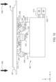
FIG. 1 is a plan view of a cluster tool assembly 100 with a single transfer chamber assembly 150. The cluster tool assembly 100 includes a plurality of load lock chambers 130, a plurality of robot chambers 180 adjacent to the plurality of load lock chambers 130, a plurality of prep chambers 190 adjacent to the plurality of robot chambers 180, and the transfer chamber assembly 150 adjacent to the plurality of robot chambers 180. The load lock chambers 130 of the cluster tool assembly 100 are typically coupled to a plurality of Front Opening Unified Pods (FOUPs) 110 by a Factory Interface (FI) 120 adjacent to the FOUPs 110.
The plurality of FOUPs 110 may be utilized to safely secure and store substrates as the substrates are moved between different machines. The plurality of FOUPs 110 may vary in quantity depending upon the process and throughput of the system. The FI 120 is disposed between the plurality of FOUPs 110 and the plurality of load lock chambers 130. The FI 120 creates an interface between the factory and the cluster tool assembly 100. The plurality of load lock chambers 130 are connected to the FI 120 by first valves 125, such that a substrate may be transferred from the FI 120 to the plurality of load lock chambers 130 through the first valves 125 and from the plurality of load lock chambers 130 to the FI 120. As shown, the first valves 125 are on one wall of the load lock chambers 130. In some embodiments, the first valves 125 are fluid isolation valves and form a seal between the FI 120 and the load lock chambers 130. This seal may keep outside contaminants from entering the cluster tool assembly 100. The load lock chambers 130 also comprise a second valve 135 on an opposite wall from the first valve 125. The second valve 135 interfaces the load lock chambers 130 with the robot chambers 180.
The transfer chamber assembly 150 includes a central transfer apparatus 145 and a plurality of processing regions 160. The plurality of processing regions 160 are disposed around the central transfer apparatus 145, such that the plurality of processing regions 160 are disposed radially outward of the central transfer apparatus 145 in the transfer chamber assembly 150.
As shown, the robot chambers 180 are on one side of the load lock chambers 130, such that the load lock chambers 130 are between the FI 120 and the robot chambers 180. The robot chambers 180 include a transfer robot 185. The transfer robot 185 may be any robot suitable to transfer one or more substrates from one chamber to another. The transfer robot 185 is utilized to transfer substrates 186 to an electrostatic chuck (e.g., electrostatic chuck) 187 that is temporarily connected to the central transfer apparatus 145. The connection between the electrostatic chuck 187 and the central transfer apparatus 145 is described below in more detail. The electrostatic chuck 187 holds a single substrate 186 and travels with the substrate 186 into each of the processing regions 160. The electrostatic chuck 187, when in one of the processing regions 160 (with a substrate thereon), forms a boundary of the processing region 160. The substrates 186 are mated with one electrostatic chuck 187, and the substrate 186 moves in and between the processing regions 160 on that electrostatic chuck 187.
In some embodiments, the transfer robot 185 is configured to transport substrates 186 from the load lock chambers 130 and into the plurality of prep chambers 190. The transfer robot 185 removes the substrate 186 from the load lock chambers 130, moves the substrate 186 into the robot chamber 180, and then moves the substrate 186 into the prep chamber 190. The transfer robot 185 is also be configured to move substrates 186 to the transfer chamber assembly 150. Similarly to how the substrate 186 may be moved to the prep chambers 190 from the load lock chambers 130 by the transfer robot 185, the substrate 186 may also be moved from the prep chamber 190 to the load lock chambers 130 by the transfer robot 185. The transfer robot 185 may also move substrates 186 from the transfer chamber assembly 150 to the prep chambers 190 or the load lock chambers 130. In some alternative embodiments, the transfer robot 185 may move a substrate 186 from the load lock chambers 130, move the substrate 186 into the robot chamber 180, and then move the substrate 186 into the transfer chamber assembly 150. In this alternative embodiment, the substrate 186 may not enter the prep chamber 190 either before processing in the transfer chamber assembly 150 or after processing in the transfer chamber assembly 150.
The prep chambers 190 include a cleaning chamber 192, a packaging structure 194, and a cleaning chamber vacuum pump 196. The cleaning chamber 192 may be any one of a pre-clean chamber, an anneal chamber, or a cool down chamber, depending upon the desired process within the cluster tool assembly 100. In some embodiments, the cleaning chamber 192 is a wet clean chamber. In other embodiments, the cleaning chamber 192 is a plasma clean chamber. In yet other exemplary embodiments, the cleaning chamber 192 is a Preclean II chamber available from Applied Materials, Inc., of Santa Clara, Calif.
The packaging structure 194 may be a structural support for the cleaning chamber 192. The packaging structure 194 may include a sub-transfer chamber (not shown), a gas supply (not shown), and an exhaust port (not shown). The packaging structure 194 may provide the structure around the cleaning chamber 192 and interface the cleaning chamber 192 to the robot chamber 180. The cleaning chamber vacuum pump 196 is disposed adjacent to a wall of the cleaning chamber 192 and provides control of the pressure within the cleaning chamber 192. One cleaning chamber vacuum pump 196 may be adjacent to each of the cleaning chambers 192. The cleaning chamber vacuum pump 196 may be configured to provide a pressure change to the cleaning chamber 192. In some embodiments, the cleaning chamber vacuum pump 196 is configured to increase the pressure of the cleaning chamber 192. In other embodiments, the cleaning chamber vacuum pump 196 is configured to decrease the pressure of the cleaning chamber 192, such as to create a vacuum within the cleaning chamber 192. In yet other embodiments, the cleaning chamber vacuum pump 196 is configured to both increase and decrease the pressure of the cleaning chamber 192 depending on the process being utilized within the cluster tool assembly 100. The cleaning chamber vacuum pump 196 may be held in place by the packaging structure 194, such that the packaging structure 194 at least partially surrounds the cleaning chamber vacuum pump 196.
The load lock chambers 130, robot chambers 180, and prep chambers 190 may be arranged to reduce the footprint required for the cluster tool assembly 100. In one embodiment, one load lock chamber 130 is attached to a first wall of the robot chamber 180. One prep chamber 190 is attached to a second wall of the robot chamber 180. The first and second walls may be adjacent walls on the robot chamber 180. In some embodiments, the robot chamber 180 is roughly square shaped. In other embodiments, the robot chamber 180 is a quadrilateral. In yet other embodiments, the robot chambers 180 may be any desired shape, such as a polygon or a round shape, such as a circle. In an embodiment where the robot chambers 180 are a square or quadrilateral shape, the first wall and the second wall may be adjacent walls, such that the two walls intersect each other. As shown in FIG. 1 , the cluster tool assembly 100 includes two load lock chambers 130, two robot chambers 180, and two cleaning chambers 190. The two load lock chambers 130, two robot chambers 180, and two cleaning chambers 190, when arranged as described above, form two transport assemblies. The two transport assemblies are spaced apart from each other and form mirror images of one another, such that the prep chambers 190 are on opposite walls of their respective robot chambers 180.
As shown, the transfer chamber assembly 150 is adjacent to the robot chambers 180, such that the transfer chamber assembly 150 is connected to the robot chambers 180 by a valve (not shown). The transfer chamber assembly 150 may be attached to a third wall of the robot chambers 180. The third wall of the robot chambers 180 may be opposite the first wall of the robot chambers 180.
A chamber pump 165 is disposed adjacent to each of the processing regions 160, such that a plurality of chamber pumps 165 are disposed around the central transfer apparatus 145. The plurality of chamber pumps 165 may also be disposed radially outward of the central transfer apparatus 145 in the transfer chamber assembly 150. One chamber pump 165 for each of the processing regions 160 is provided, such that one chamber pump 165 is connected to each of the processing regions 160. In some embodiments, multiple chamber pumps 165 per processing region 160 are provided. In yet other embodiments, a processing region 160 may not have a chamber pump 165. A varying number of chamber pumps 165 per processing region 160 may be provided, such that one or more processing regions 160 may have a different number of chamber pumps 165 than a separate set of processing regions 160. In some embodiments, the chamber pumps 165 are configured to increase the pressure of the processing region 160. In other embodiments, the chamber pumps 196 are configured to decrease the pressure of the processing region 160, such as to create a vacuum within the processing region 160. In yet other embodiments, the chamber pumps 165 are configured to both increase and decrease the pressure of the processing regions 160 depending on the process being utilized within the cluster tool assembly 100.
In the embodiment shown in FIG. 1 , the transfer chamber assembly 150 includes six processing regions 160. In one embodiment, the transfer chamber assembly 150 includes a single processing region 160. In another embodiment, two or more processing regions 160 are provided. In some embodiments two to twelve processing regions 160 are within the transfer chamber assembly 150. In other embodiments, four to eight processing regions 160 are within the transfer chamber assembly 150. The number of processing regions 160 impacts the total footprint of the cluster tool assembly 100, the number of possible process steps capable of being performed by the cluster tool assembly 100, the total fabrication cost of the cluster tool assembly 100, and the throughput of the cluster tool assembly 100.
The plurality of processing regions 160 can be any one of PVD, CVD, ALD, etch, cleaning, heating, annealing, and/or polishing platforms. In some embodiments, the plurality of processing regions 160 can all be similar platforms. In other embodiments, the plurality of processing regions 160 can include two or more types of processing platforms. In one exemplary embodiment, all of the plurality of processing regions 160 are PVD process chambers. In another exemplary embodiment, the plurality of processing regions 160 includes both PVD and CVD process chambers. Other embodiments of the makeup of the plurality of processing regions 160 are envisioned. The plurality of processing regions 160 can be altered to match the types of process chambers needed to complete a process.
The central transfer apparatus 145 is disposed in the center of the transfer chamber assembly 150, such that the central transfer apparatus 145 is disposed around a central axis of the transfer chamber assembly 150. The central transfer apparatus 145, may be any suitable transfer device. The central transfer apparatus 145 is configured to transport a substrate 186 on an electrostatic chuck 187 to and from each of the processing regions 160. In one embodiment, the central transfer apparatus 145 is configured as a carousel system.
As shown in FIGS. 2A and 2B, a processing region 160 is serviced via a central transfer apparatus (e.g., the central transfer apparatus 145 of FIG. 1 ) to transfer electrostatic chucks (e.g., the electrostatic chuck 187) and substrates (e.g., the substrate 186) into and out of the processing region 160. A substrate transfer opening 204 extends inwardly of the outer surface of a circumferential wall of the processing region 160 and into a transfer region 201 of the processing region 160. The transfer opening 204 allows the transfer robot 185, to transfer the substrate 186 into and out of the transfer region 201. In various embodiments, the transfer opening 204 may be omitted. For example, in embodiments where the processing region 160 does not interface with the transfer robot 185, the transfer opening 204 may be omitted.
A source assembly 270 of the processing region 160 is configured to perform a deposition process (e.g., a PVD deposition process or the like). In this configuration, the source assembly 270 includes a target 272, a magnetron assembly 271, a source assembly wall 273, a lid 274, and a sputtering power supply 275. The magnetron assembly 271 includes a magnetron region 279 in which the magnetron 271A is rotated by use of a magnetron rotation motor 276 during processing. The target 272 and magnetron assembly 271 are typically cooled by the delivery of a cooling fluid (e.g., DI water) to the magnetron region 279 from a fluid recirculation device (not shown). The magnetron 271A includes a plurality of magnets 271B that are configured to generate magnetic fields that extend below the lower surface of the target 272 to promote a sputtering process in the processing volume 260 during a PVD deposition process.
Alternate configurations of the processing region 160, which are adapted to perform CVD, PECVD, ALD, PEALD, etch, or thermal processes, the source assembly 270 generally include different hardware components. In one example, the source assembly 270 of a processing station that is adapted to perform a PECVD deposition process or etch process includes a gas distribution plate, or showerhead, that is configured to deliver a precursor gas or etching gas into the processing volume 260 and across a surface of a substrate disposed within the processing region 160 during processing. In this case, the magnetron assembly 271 and target are not used, and the sputtering power supply 275 is replaced with an RF power supply that is configured to bias the gas distribution plate.
A substrate support actuation assembly 290 includes a pedestal lift assembly 291 and a pedestal assembly 224. The pedestal lift assembly 291 includes a lift actuator assembly 268 and a lift mounting assembly 266, which is coupled to the base 219 of the processing region 160. During operation the lift actuator assembly 268 and lift mounting assembly 266 are configured to position the pedestal assembly 224 in at least a transfer position (FIG. 2A), which is positioned vertically (in the Z direction) below a transfer arm 210 of the central transfer apparatus 145 (i.e., transfer plane), and a processing position (FIG. 2B), which is vertically above the transfer arm 210. Further, the lift actuator assembly 268 and the lift mounting assembly 266 apply vertical motion, in the +Z direction, to the pedestal assembly 224 to pick the electrostatic chuck 187 off of the transfer arm 210. Additionally, the lift actuator assembly 268 and the lift mounting assembly 266 apply vertical motion, in the −Z direction, to the pedestal assembly 224 to position the electrostatic chuck 187 on the transfer arm 210.
The lift actuator assembly 268 is coupled to a pedestal shaft 292, which is supported by bearings (not shown) that are coupled to a base 219 of the transfer chamber assembly 150 to guide the pedestal shaft 292 as it is translated by the lift actuator assembly 268. A bellows assembly (not shown) is used to form a seal between the outer diameter of the pedestal shaft 292 and a portion of the base 219, such that a vacuum environment created within the transfer region 201 by use of a pump 254 is maintained during normal operation.
The pedestal assembly 224 includes a substrate support 226 that is coupled to the pedestal shaft 292. The pedestal assembly 224 includes a heater power source 295, an electrostatic chuck power source 296 and a backside gas source 297. The substrate support 226 supports the electrostatic chuck 187 and the substrate 186 within the processing region 160.
The substrate support 226 comprises pins 240 and 242. The pins 240 are coupled to the heater power source 295. The pedestal assembly 224 includes two or more pins 240. Further, the pins 240 are configured to mate (e.g., physically and electrically couple) with terminals 214 of the electrostatic chuck 187. The heater power source 295 provides an AC power signal or signals. The heater power source 295 provides an AC power signal having a current in a range of about 20 A to about 30 A to the pins 240 which is provided to the heating elements (e.g., heating elements 372 of FIG. 3 ) via the terminals 214 when the pins 240 are mated with the terminals 214. In other embodiments, the heater power source 295 provides an AC power signal having a current of less than 20 A, or greater than 30 A.
The pins 242 of the substrate support 226 mate with terminals 216 of the electrostatic chuck 187. The substrate support 226 includes two or more pins 242. In such embodiments, each of the pins 242 is configured to couple to a different one of the terminals 216. For example, a first one of the pins 242 is configured to couple to a first one of the terminals 216 and a second of the pins 242 is configured to couple to a second one of the terminals 216. The pins 242 are coupled to the electrostatic chuck power source 296.
The electrostatic chuck power source 296 provides DC power signals to the pins 242. The pins 242 couple the DC power signals to the terminals 216 and to chucking electrodes (e.g., the chucking electrodes 370 of FIG. 3 ) when the pins 242 are mated with the terminals 216 to electrically chuck the substrate 186 to the electrostatic chuck 187. In one embodiment, the electrostatic chuck power source 296 provides a positive DC power signal to a first one of the pins 242 and a negative DC power signal to a second one of the pins 242 to electrically chuck the substrate 186 to the electrostatic chuck 187. The DC power signals drive the pins 242, the terminals 212, and the chucking electrodes 370 in a bi-polar configuration such that a first DC power signal is positive and a second DC power signal is negative. The magnitudes of the DC power signals may be the same. For example, the first DC power signal is about 1500 V and the second DC power signal is about −1500 V. Alternatively, the DC power signals have a magnitude greater than or less than about 1500 V. In other embodiments, the magnitude of a first one of the DC power signals differs from the magnitude of a second one of the DC power signals.
The pins 240 and 242 are removably coupled or non-removably (or permanently) coupled to the pedestal assembly 224. For example, in one embodiment, the pins 240 and/or 242 are removably coupled and may be attached and removed from the pedestal assembly 224 such that the pins 240 and/or 242 may be replaced without damaging the pedestal assembly 224. The contact between the pins 240 and 242 and the terminals 214 and 212 causes wear to the pins 240 and 242. Over time, the pins 240 and 242 may need to be replaced. Removably coupling the pins 240 and 242 to the pedestal assembly 224 allows the pins 240 and 242 to be removed and replaced when wear affects the operation of the pins 240 and/or 242 and degrades the coupling between the pins 240, 242 and the terminals 214, 212.
The pedestal assembly 224 includes flexible element 280. The flexible element 280 includes a passageway 282 and bellows 284. The flexible element 280 is configured to generate a seal against a bottom surface of the electrostatic chuck 187. A backside gas is provided via the backside gas source 297 to the passageway 282 of the flexible element 280. The backside gas flows through the passageway 282 into the space between the substrate 186 and the electrostatic chuck 187 to improve the uniformity of the thermal conductivity between the substrate 186 and the electrostatic chuck 187, improving the uniformity of the deposition of materials onto the substrate 186. The backside gas may be nitrogen, helium, or argon, among others.
A process kit assembly 230 generally includes a process region shield 232 and a sealing assembly 235. A station wall 234 includes a first port that is coupled to a vacuum pump 265 and is configured to evacuate a processing volume 260 through a circumferential gap formed between an upper portion of the shield 232, lower surface of the target 272 and a portion of an isolation ring 233 and station wall 234 during processing. The station wall 234 is coupled to a gas source assembly 289, and is configured to deliver one or more process gases (e.g., Ar, N2) to the processing volume 260 through a circumferential plenum during processing.
During processing of a substrate, e.g., FIG. 2B, the substrate 186 and the electrostatic chuck 187 are positioned in a processing position below the source assembly 270. When in the processing position a region 284 of the electrostatic chuck 187 forms a “seal” with a portion of the sealing assembly 235 so as to substantially fluidly isolate the processing volume 260 from the transfer region 201. Thus, in the processing position, the electrostatic chuck 187, the sealing assembly 235, the process region shield 232, the station wall 234, the isolation ring 233 and target 272 substantially enclose and define the processing volume 260. In some embodiments, the “seal” formed between the portion of the electrostatic chuck 187 and an upper plate 235 a of the sealing assembly 235 is created at a sealing region that is formed by physical contact between a surface of the region 264 of the electrostatic chuck 187 and a surface of the upper plate 235 a. In some embodiments, a flexible bellows assembly 235 b of the sealing assembly 235 is configured to be extended in the vertical direction as the portion of the electrostatic chuck 187 is placed in contact with the surface of the portion of the sealing assembly 235 by use of the lift actuator assembly 268 in the substrate support actuation assembly 290. The compliant nature of the flexible bellows assembly allows any misalignment or planarity differences between the surface of the portion of the electrostatic chuck 187 and the surface of the portion of the sealing assembly 235 to be taken up so that a reliable and repeatable seal can be formed at the region 264. The flexible bellows assembly 235 b may be a stainless steel bellows assembly or Inconel bellows assembly, among others.
FIG. 3 is a schematic sectional side view of a portion of one of the transfer arms 210 of the central transfer apparatus 145. Electrical contacts 253 are at a second end 225 of the transfer arm 210. Also shown is the electrostatic chuck 187 supported by the electrical contact 253. A substrate 186 is shown attached to the electrostatic chuck 187.
Each of the electrical contacts 253 may be shaped as a protruding member or pin. The electrical contacts 253 a and 253 b contact and form an electrical connection with the terminals 212 of the electrostatic chuck 187. Additionally, or alternatively, the electrical contacts 253 c and 253 d contact and form an electrical connection with one or more of the terminals 214. In one or more embodiments, the electrical contacts 253 c and 253 d are omitted such that the transfer arm 210 includes the electrical interface connects 253 a and 253 b, and not the electrical contacts 253 c and 253 d.
The electrical contacts 253 provide electrical power to an electrical component or components within the electrostatic chuck 187 while the electrostatic chuck 187 and substrate 186 are supported by the transfer arm 210. For example, the electrical contacts 253 a and 253 b are coupled to a power supply 258 that provides DC signals, e.g., a DC power supply, via connections 350 a. The DC signals are supplied to the chucking electrodes (e.g., chucking electrodes 370 of FIGS. 3 and 4 ) via the electrical connection between the electrical contacts 253 a, 253 b and the terminals 212. A first one of the DC signals has a positive polarity and a second one of the DC signals has a negative polarity. Further, the magnitude of the DC signals are substantially similar (e.g., within five percent of each other). For example, the magnitude of the DC signals is about 1500 V. Alternatively, the magnitude of the DC signals is less than or greater than about 1500 V. Driving the chucking electrodes 370 with the DC signals generates an electrical chucking force that holds the substrate 186 to the surface of the electrostatic chuck 187.
The power supply 256 provides an alternating current (AC) signal or signals that is provided to the heating elements (e.g., heating elements 372 of FIGS. 3 and 4 ) via the electrical connection between an electrical contact 253 and a terminal 214. The power supply 256 is connected to the electrical contacts 253 c and 253 d via connections 350 b. The power supply 256 may be referred to as an AC power supply. The AC signal provides a current of about 30 A. Alternatively, the AC signal provides a current of less than or greater than 30 A. The AC signal or signals are converted by the heating elements 372 into heat that thermally couples with the substrate 186.
The connections (conductors) 350 are routed through an internal region of the transfer arm 210 to connect with the respective ones of the electrical contacts 253.
FIG. 4 illustrates a portion of the pedestal assembly 224, the electrostatic chuck 187, and the substrate 186. In the embodiment of FIG. 4 , substrate support 226 has pins 240 and 242 that are coupled to terminals 214 and 216, respectively. The pins 240 receive an AC power signal from heater power source 295 and couple the AC power signal to the terminals 214. The terminals 214 are connected to the heating elements 372 and receive the AC power signal from the terminals 214. The heating elements 372 generate heat from the AC power signals which is thermally coupled to the substrate 186.
The pins 242 of the substrate support 226 mate with the terminals 216 of the electrostatic chuck 187 and couple DC power signals to the terminals 216 from the power source 296. The DC power signals are communicated from the terminals 216 to the chucking electrodes 370 to electrostatic chuck the substrate 186 to the surface of the electrostatic chuck 187. First and second DC power signals are driven onto the terminals 216 such that a first DC power signal is driven onto chucking electrode 370A or 370B and a second DC power signal is driven on the other one of the chucking electrode 370A or 370B. The first and second DC power signals have a similar magnitude but differ in polarity.
The flexible element 280 forces a seal with the surface 311 of the electrostatic chuck 187 such that a backside gas may be provided into the space or spaces between the substrate 186 and the surface 312 of the electrostatic chuck 187 via the passageway 317 of the electrostatic chuck 187. The passageway 317 is fluidly coupled with the passageway 282. The backside gas improves the thermal coupling between the electrostatic chuck 187 and the substrate 186, increasing the uniformity of thermal coupling between the electrostatic chuck 187 and the substrate 186, improving the process uniformity on the substrate 186.
FIG. 5 illustrates an example pin 500, according to one or more embodiments. One or more of the pins 240 and 242 may be configured similar to that of the pin 500 such that the surface of one or more of the pins 240 and 242 have a substantially flat surface 510. The surface 510 is substantially flat such that the surface 510 does not significantly vary in the +Z or −Z direction.
FIG. 6 illustrates an example pin 600, according to one or more embodiments. One or more of the pins 240 and 242 may be configured similar to that of the pin 600. The pin 600 includes a convex surface 610. The convex surface 610 has a radius of about 5 mm to about 20 mm. Alternatively, the convex surface 610 may have a radius of less than 5 mm or greater than 20 mm.
FIG. 7 illustrates an example pin 700, according to one or more embodiments. One or more of the pins 240 and 242 may be configured similar to that of the pin 600. The surface of the pin 600 includes a convex portion 710. The convex portion 710 has a radius of about 5 mm to about 20 mm. Alternatively, the convex portion 710 may have a radius of less than 5 mm or greater than 20 mm. Further, the convex portion 710 includes a flat portion 712 in a central area of the convex portion 710.
FIG. 8 illustrates an example pin 800, according to one or more embodiments. One or more of the pins 240 and 242 may be configured similar to that of the pin 800. The surface of the pin 800 includes a groove 810. The groove 810 has a depth of 812 from the surface 814 of the pin 800 in the −Z direction. The depth 812 allows a portion (e.g., at least a tip) of a terminal (e.g., the terminal 212, 214, and/or 216) to contact the internal inclined surfaces of the groove 810.
FIG. 9 illustrates an example pin 900, according to one or more embodiments. One or more of the pins 240 and 242 may be configured similar to that of the pin 900. The surface of the pin 900 includes concave portion 910. The concave portion 910 has a radius of 912. The concave portion 910 has a radius 912 of about 5 mm to about 20 mm. Alternatively, the concave portion 910 may have a radius of less than 5 mm or greater than 20 mm.
The pins 500, 600, 700, 800, and/or 900 may be comprised of molybdenum (Mo) or tungsten (W), or a combination thereof. Alternatively, the pins 500, 600, 700, 800, and/or 900 may be comprised of a material other than Mo or W, or a combination of materials including or not including Mo and W. Further, the pins 500, 600, 700, 800, and/or 900 has a surface roughness in a range of about 2 Ra to about 6 Ra. Alternatively, the pins 500, 600, 700, 800, and/or 900 may have a surface roughness of less than 2 Ra or greater than about 6 Ra.
The terminals 212, 214, and 216 and the pins 240 and 242 may be comprised of similar materials or different materials. For example, the terminals 212, 214, and 216 and the pins 240 and 242 may be formed of a first material (e.g., Mo or W, among others). Alternatively, the terminals 212, 214, and 216 are formed from a first material or materials and the pins 240 and 242 are formed from a second material or materials.
The terminals 212, 214, and 216 and the pins 240 and 242 may have a similar shape. For example, the terminals 212, 214, and 216 and the pins 240 and 242 have a common one of a flat, a convex, concave, and a grooved shape. In other embodiments, the terminals 212, 214, and 216 have one of a flat, convex, concave, and a grooved shape and the pins 240 and 242 have a different one of a flat, convex, concave, and a grooved shape. In one example embodiment, the terminals 212, 214, 216 have a flat shape and the pins 240, 242 have a convex shape.
FIG. 10 is a schematic illustration of the substrate support 226 and the electrostatic chuck 287, according to one or more embodiments. As illustrated in FIG. 10 , the pins 240 are coupled to a power source (e.g., the power source 296) via traces 1010. Further, the pins 242 are coupled to a power source (e.g., the power source 295) via the traces 1020. The traces 1010 and 1020 may be routed through an internal region of the pedestal assembly 224.
The pins 240 are secured to the substrate support 226 via fasteners 1030, and the pins 242 are secured to the substrate support 226 via fasteners 1031. The fasteners 1030 and 1031 may be a nut or similar type of fastener device. In one embodiment, the fasteners 1030 and 1031 may be removed such that the pins 240 and 242 may be replaced. For example, removing the fastener 1030 allows the pins 240 to be removed and a new pin 240 coupled to the substrate support 226 via the fastener 1030. Further, removing the fastener 1031 allows the pins 242 to be removed and a new pin 242 coupled to the substrate support 226 via the fastener 1031.
FIG. 11 illustrates the interface between an alignment element 1060 of the substrate support 226 and a centering element 218 of the electrostatic chuck 287. When the electrostatic chuck 287 is positioned on the substrate support 226, each of the centering elements 218 of the electrostatic chuck 287 interfaces with one of the alignment elements 1060, centering the electrostatic chuck 287 over the substrate support 226. Utilizing the alignment elements 1060 and the centering elements 218 centers the electrostatic chuck 287 with the substrate support 226 and aligns the passageway 282 with the passageway 317 of the electrostatic chuck 287. Centering the electrostatic chuck 287 with the substrate support 226 aligns the flexible element 280 with the passageway 317, the terminals 214 with the pins 240 and the terminals 216 with the pins 242.
The pins 240 include one or more compliance elements. For example, as illustrated in FIG. 12 , the pin 242 a comprises an interface element 1210, a compliance element 1220, and a base 1230. The compliance element 1220 is positioned on the base 1230 and supports the interface element 1210, controlling the movement of the interface element 1210 in the Z direction. For example, in response to an external force, the compliance element 1220 allows interface element 1210 to travel in the −Z direction in response to a force (e.g., the force 1090 in FIG. 10 ). The compliance element 1220 controls the amount that the interface element 1210 travels in the −Z direction and returns the interface element 1210 to a starting point when a force (e.g., the force 1090) is removed. Each of the pins 240 includes an interface element 1210, a compliance element 1220, and a base 1230 as well. Further, the compliance element 1220 for each pin 240 may be configured similarly, or one or more of the compliance elements 1220 may be configured differently from a second one or more compliance element 1220. For example, in one or more embodiments, each of the compliance elements 1220 allows the corresponding interface element 1210 to travel the same distance in the −Z direction in response to a common amount of force. Alternatively, a first one or more of the compliance elements 1220 is more restrictive regarding the movement of a corresponding interface element 1210 in the −Z direction than a second one or more of the compliance elements 1220.
As illustrated in FIG. 10 , the electrostatic chuck 287 and the substrate 286 apply a force 1090 to the pins 240 and 242, and the flexible element (e.g., the flexible element 280 of FIG. 4 ) of the substrate support 226. At least a portion of the force 1090 generates the coupling between the pins 240, 242 and the terminals 214, 216. Further, at least a portion of the force 1090 generates the coupling between the flexible element 280 and the electrostatic chuck 287. The force 1090 is the combined weight of the electrostatic chuck 287 and the substrate 286. The weight of the electrostatic chuck 287 and the substrate 286 may be in a range of about 4 lb. to about 8 lb. Alternatively, the weight of the electrostatic chuck 287 and the substrate 286 may be less than about 4 lb. or greater than 8 lb.
The compliance element 1220 controls the distance that interface element 1210 travels in the −Z direction is response to receiving the electrostatic chuck 287 and the substrate 286. For example, the compliance element 1220 controls the movement of the interface element 1210 in the −Z direction such that that each of the pins 240 and 242 are sufficiently coupled with a corresponding one of the terminals 214 and 216 and AC or DC power signals may be driven onto the terminals 214 and 216 form corresponding ones of the pins 240 and 242.
In one embodiment, the compliance element 1220 is a spring. The compliance element 1220 may be a compression spring that compresses in response to an input force. As illustrated in FIG. 12 , the compliance element 1220 may have an angled shape. Alternatively, as illustrated in FIG. 13 , a compliance element 1320 includes one or more spring elements. The spring elements may be spring disks (e.g., the spring disks 1410 of FIG. 14 ). The compliance element 1320 may have a single spring disk 1410 or multiple spring disks 1410. Further, the spring disks 1410 may be disclosed in parallel with each other (e.g., compliance element 1420), in series with other (e.g., compliance element 1422), or a combination thereof (e.g., compliance element 1424). The number of the spring disks 1410 in a compliance member may be one or more. In one embodiment, the number of spring disks in a compliance member is four or more. In one or more embodiments, the compliance element 1220 is a device other than a spring and that is able to control the movement of the interface element 1210 in the Z direction.
The compliance element 1220 may have a spring constant of about 2 lb/mm to about 3 lb/mm. However, in other embodiments, spring constants of less than about 2 lb/mm or greater than about 3 lb/mm may be utilized. Further, the spring force may be about 3 lb/mm to about 4 lb/mm. The compression of the compliance element 1220 may be about 0.2 mm to about 0.7 mm. Alternatively, the compression of the compliance element 1220 may be less than about 0.2 mm or greater than about 0.7 mm. The compliance force for the pin 242 a is about 1.3 lb/mm to about 1.6 lb/mm. However, in other embodiments, the compliance force for the pin 242 a is less than about 1.3 lb/mm or greater than about 1.6 lb/mm. Further, the total spring force of the compliance element 1220 is about 2.5 lb/mm to about 3 lb/mm. Alternatively, the total spring force of the compliance element 1220 is less than 2.5 lb/mm or greater than about 3 lb/mm.
As stated above, the compliance element 1220 controls the amount that the interface element 1210 travels in the −Z direction when an external force is applied. Controlling the travel of the interface element 1210 ensures that sufficient contact is present between the pins 240 and 242 and the terminals 214 and 216 such that the AC and DC power signals are coupled from the pins 240 and 242 to the terminals 214 and 216. When no force (e.g., no load) is applied to the pins 240, the corresponding compliance element (e.g., the compliance element 1220) is not compressed and the compliance element places the interface element (e.g., the interface element 1210) of each pin 240 in the extended position. No force is applied to the pins 242 when an electrostatic chuck (e.g., the electrostatic chuck 287) and a substrate (e.g., the substrate 286) are not in contact with the substrate support 226. Further, in such an embodiment, the substrate support 226 is moved in the −Z direction away from the sealing assembly 235.
FIG. 15 illustrates the pins 240 coupled to a compliance element 1510. The compliance element 1510 is coupled to each of the pins 240. The compliance element 1510 may be a flexure mechanism configured to control the movement of the pins 240 in the −Z direction in response to a force (e.g., force 1090) similar to that of the compliance element 1220.
The pins 240 are configured to aid in leveling the electrostatic chuck 287 and the substrate 286. As illustrated in FIG. 16 , the pin 240A is configured to level the electrostatic chuck 287 and the substrate 286. For example, the pin 240 a includes an interface element 1620 and a leveling element 1610. The interface element 1620 is configured to interface with one of the terminals 214. The leveling element 1610 flexes in the −Z direction in response to the weight of the electrostatic chuck 287 and the substrate 286. Each of the pins 240 is configured similar to that of the pin 240 a. Accordingly, as each of the leveling elements 1610 flex (e.g., move) in the −Z direction, in response to the force 1090, the surface of the substrate 286 is leveled. The leveling elements 1610 provide about +/−2 mm of movement. Alternatively, the leveling elements 1610 provide less than about +/−2 mm or more than +/−2 mm of movement. Each of the leveling elements 1610 may provide a common amount movement or different amounts of movement according to the weight of the electrostatic chuck 287 and the substrate 286 to level the substrate 286.
Referring to FIGS. 2A and 2B, the electrostatic chuck 287 and the substrate 286 are loaded into the processing region 160 via a transfer arm 210 of the central transfer apparatus 145 and positioned over the pedestal assembly 224. The pedestal lift assembly 291 moves the substrate support 226 vertically toward the electrostatic chuck 287 such that the alignment elements 1060 interface with the centering elements 218, centering the electrostatic chuck 287 with the substrate support 226. The initial force applied by the electrostatic chuck 287 and the substrate 286 corresponds to the combined weight of the electrostatic chuck 287 and the substrate 286. For example, the initial force applied by the electrostatic chuck 287 and the substrate 286 is about 5 lb to about 10 lb. Further, the pins 240 and 242 do not contact the terminals 214 and 216. Alternatively, the pins 240 and 242 partially contact the terminals 214 and 216, however, the pins 240 and 242 do not support the weight of the electrostatic chuck 287 and the substrate 286.
The pedestal lift assembly 291 further moves the substrate support 226 about 8 mm to about 12 mm in the +Z direction such that the pins 242 contact the terminals 216. Alternatively, the pedestal lift assembly 291 moves the substrate support 226 less than about 8 mm or greater than about 12 mm, or another distance in the +Z direction such that the pins 242 contact the terminals 216. The pins 242 support about 5 percent to about 10 percent of the weight of the electrostatic chuck 287 and the substrate 286. The pins 242 include a compliance element (e.g., the compliance element 1220) that aids in establishing an electrical contact between the interface element (e.g., the interface element 1210) and a respective one of the terminals 216.
The pedestal lift assembly 291 moves the substrate support 226 about 0.5 mm to about 2.5 mm to establish an interface between the flexible element 280 and the electrostatic chuck 287. Alternatively, the pedestal lift assembly 291 moves the substrate support 226 greater than 0 mm but less 0.5 mm or greater than 2.5 mm, or another distance in the +Z direction such that flexible element 280 contacts the bottom of the electrostatic chuck 287.
The flexible element 280 supports about 20 percent to about 30 percent of the force 1090 (e.g., weight of the electrostatic chuck 287 and the substrate 286). Alternatively, the flexible element 280 supports less than about 20 percent or more than about 30 percent of the weight of the electrostatic chuck 287 and the substrate 286. In various embodiments, the amount of weight supported by the flexible element 280 (e.g., the amount of force in the −Z direction) generates a seal between the flexible element 280 and the bottom of the electrostatic chuck 287.
The pedestal lift assembly 291 moves the substrate support 226 about 1 mm to about 3 mm to establish an interface between the pins 240 and the terminals 214. Alternatively, the pedestal lift assembly 291 moves the substrate support 226 less than about 1 mm or greater than about 3 mm. The pedestal lift assembly 291 moves the substrate support 226 to generate a coupling between the pins 240 and the terminals 214. The amount of weight supported by each of the pins 240 is about 1.25 lb to about 1.75 lb. Alternatively, the amount of weight supported by each of the pins 240 is less than about 1.25 lb or greater than about 1.75 lb. The amount of weight supported by each pin 240 forms an electrical contact between the pin 240 and the terminal 214.
While the foregoing is directed to embodiments of the present disclosure, other and further embodiments of the disclosure may be devised without departing from the basic scope thereof, and the scope thereof is determined by the claims that follow.

Claims (20)

What is claimed is:
1. A pedestal assembly for a processing region, the pedestal assembly comprising:
a substrate support;
first pins coupled to the substrate support, configured to mate with first terminals of an electrostatic chuck, and configured to be coupled to a first power source, each of the first pins comprises:
an interface element; and
a compliance element supporting the interface element;
second pins coupled to the substrate support, configured to mate with second terminals of the electrostatic chuck, and configured to be coupled to a second power source;
alignment elements coupled to the substrate support and configured to interface with centering elements of the electrostatic chuck; and
a flexible element coupled to the substrate support, configured to interface with a passageway of the electrostatic chuck, and configured to couple to a gas source.
2. The pedestal assembly of claim 1, wherein the first pins are configured to support a first portion of a weight of the electrostatic chuck.
3. The pedestal assembly of claim 2, wherein the compliance element of each of the first pins is configured to control movement of the interface element of a corresponding one of the first pins in response to the first portion of the weight of the electrostatic chuck.
4. The pedestal assembly of claim 3, wherein the compliance element of each of the first pins is a spring having a spring constant of about 2 lb/mm to about 3 lb/mm.
5. The pedestal assembly of claim 2, wherein the flexible element is configured to support a second portion of the weight of the electrostatic chuck, the first portion differs from the second portion.
6. The pedestal assembly of claim 1, wherein at least one pin selected from the group consisting of the first pins and the second pins has a flat surface, concave surface, convex surface, or a grooved surface.
7. The pedestal assembly of claim 6, wherein at least one pin selected from the group consisting of the first pins and the second pins has a surface roughness in a range of about 2 Ra to about 6 Ra.
8. The pedestal assembly of claim 1, wherein the first pins and the second pins are removably coupled to the substrate support.
9. The pedestal assembly of claim 1, wherein a pedestal lift assembly is configured to apply vertical motion to the substrate support.
10. A processing region comprising:
a sealing assembly; and
a pedestal assembly configured to move between a processing position and a transfer position, the pedestal assembly comprising:
a substrate support;
first pins coupled to the substrate support, configured to mate with first terminals of an electrostatic chuck, and configured to couple to a first power source, each of the first pins comprises:
an interface element; and
a compliance element supporting the interface element;
second pins coupled to the substrate support, configured to mate with second terminals of the electrostatic chuck, and configured to couple to a second power source;
alignment elements coupled to the substrate support and configured to interface with centering elements of the electrostatic chuck; and
a flexible element coupled to the substrate support, configured to interface with a passageway of the electrostatic chuck and configured to couple to a gas source, wherein when the pedestal assembly is the processing position, a portion of the electrostatic chuck is configured to mate with a portion of the sealing assembly to form a processing volume.
11. The processing region of claim 10, wherein the first pins are configured support a first portion of a weight of the electrostatic chuck.
12. The processing region of claim 11, wherein the compliance element of each of the first pins is configured to control movement of the interface element of a corresponding one of the first pins in response to the first portion of the weight of the electrostatic chuck.
13. The processing region of claim 12, wherein the compliance element of each of the first pins is a spring having a spring constant of about 2 lb/mm to about 3 lb/mm.
14. The processing region of claim 11, wherein the flexible element is configured to support a second portion of the weight of the electrostatic chuck, the first portion differs from the second portion.
15. The processing region of claim 10, wherein at least one pin selected from the group consisting of the first pins and the second pins has a flat surface, concave surface, convex surface, or a grooved surface.
16. The processing region of claim 10, wherein at least one pin selected from the group consisting of the first pins and the second pins has a surface roughness in a range of about 2 Ra to about 6 Ra.
17. A cluster tool assembly comprising:
a central transfer apparatus comprising a transfer arm, the transfer arm comprising first pins configured to mate with first terminals of an electrostatic chuck; and
a processing region comprising;
a pedestal assembly configured to move between a processing position and transfer position, the pedestal assembly comprising:
a substrate support;
second pins coupled to the substrate support, configured to mate with second terminals of the electrostatic chuck, and configured to couple to a first power source, each of the second pins comprises:
an interface element; and
a compliance element supporting the interface element;
third pins coupled to the substrate support, configured to mate with third terminals of the electrostatic chuck, and configured to couple to a second power source;
alignment elements coupled to the substrate support and configured to interface with centering elements of the electrostatic chuck; and
a flexible element coupled to the substrate support, configured to interface with a passageway of the electrostatic chuck and configured to couple to a gas source.
18. The cluster tool assembly of claim 17, wherein the second pins are configured support a first portion of a weight of the electrostatic chuck, and wherein the compliance element of each of the second pins is configured to control movement of the corresponding interface element of each of the second pins in response to the first portion of the weight of the electrostatic chuck.
19. The cluster tool assembly of claim 18, wherein the compliance element of each of the first pins is a spring.
20. The cluster tool assembly of claim 18, wherein the flexible element is configured to support a second portion of the weight of the electrostatic chuck, the first portion differs from the second portion.
US17/016,030 2020-09-09 2020-09-09 Pedestal assembly for a substrate processing chamber Active 2041-09-01 US11600507B2 (en)

Priority Applications (1)

Application Number Priority Date Filing Date Title
US17/016,030 US11600507B2 (en) 2020-09-09 2020-09-09 Pedestal assembly for a substrate processing chamber

Applications Claiming Priority (1)

Application Number Priority Date Filing Date Title
US17/016,030 US11600507B2 (en) 2020-09-09 2020-09-09 Pedestal assembly for a substrate processing chamber

Publications (2)

Publication Number Publication Date
US20220076979A1 US20220076979A1 (en) 2022-03-10
US11600507B2 true US11600507B2 (en) 2023-03-07

Family

ID=80469282

Family Applications (1)

Application Number Title Priority Date Filing Date
US17/016,030 Active 2041-09-01 US11600507B2 (en) 2020-09-09 2020-09-09 Pedestal assembly for a substrate processing chamber

Country Status (1)

Country Link
US (1) US11600507B2 (en)

Cited By (1)

* Cited by examiner, † Cited by third party
Publication number Priority date Publication date Assignee Title
US20230060486A1 (en) * 2021-08-27 2023-03-02 Samsung Electronics Co., Ltd. Plasma generator

Citations (149)

* Cited by examiner, † Cited by third party
Publication number Priority date Publication date Assignee Title
US5281295A (en) * 1991-02-20 1994-01-25 Semiconductor Process Laboratory Co., Ltd. Semiconductor fabrication equipment
US5663884A (en) * 1991-09-05 1997-09-02 Hitachi, Ltd. Multiprocessing apparatus
US5863170A (en) 1996-04-16 1999-01-26 Gasonics International Modular process system
US5879459A (en) 1997-08-29 1999-03-09 Genus, Inc. Vertically-stacked process reactor and cluster tool system for atomic layer deposition
US6162299A (en) 1998-07-10 2000-12-19 Asm America, Inc. Multi-position load lock chamber
WO2001037317A1 (en) 1999-11-15 2001-05-25 Lam Research Corporation Plasma processing system with dynamic gas distribution control
US20020051698A1 (en) 2000-10-26 2002-05-02 Andreas Birkner Substrate conveying module and system made up of substrate conveying modile and workstation
US6440261B1 (en) 1999-05-25 2002-08-27 Applied Materials, Inc. Dual buffer chamber cluster tool for semiconductor wafer processing
US6447607B2 (en) 1999-12-28 2002-09-10 Asm Microchemistry Oy Apparatus for growing thin films
US20020170671A1 (en) 2001-05-21 2002-11-21 Minoru Matsushita Processing apparatus, transferring apparatus and transferring method
US6560896B2 (en) * 1999-12-29 2003-05-13 Asm International N.V. Apparatus, method and system for the treatment of a wafer
US6576062B2 (en) 2000-01-06 2003-06-10 Tokyo Electron Limited Film forming apparatus and film forming method
US20030109094A1 (en) 2001-10-29 2003-06-12 Seidel Thomas E. Massively parallel atomic layer deposition/chemical vapor deposition system
US6604853B2 (en) 2001-10-11 2003-08-12 Taiwan Semiconductor Manufacturing Co., Ltd Accelerated thermal stress cycle test
US6635115B1 (en) 1996-11-18 2003-10-21 Applied Materials Inc. Tandem process chamber
US20040159553A1 (en) 2000-10-13 2004-08-19 Takeshi Nogami Semiconductor manufacturing apparatus and method for manufacturing semiconductor devices
US20050005850A1 (en) 1999-07-23 2005-01-13 Semiconductor Energy Laboratory Co., Ltd. Method of fabricating an EL display device, and apparatus for forming a thin film
US20050006230A1 (en) 2001-08-31 2005-01-13 Masaki Narushima Semiconductor processing system
US20050111936A1 (en) 2003-11-10 2005-05-26 Kim Ki-Sang Multi-chamber system
US20050118009A1 (en) 2003-11-10 2005-06-02 Blueshift Technologies, Inc. Stacked process modules for a semiconductor handling system
US20050115822A1 (en) 2002-02-19 2005-06-02 Wolfram Maass Sputtering cathode and device and method for coating a substrate with several layers
DE10350517A1 (en) 2003-10-29 2005-06-09 Sieghard Schiller Gmbh & Co. Kg Holder for semiconductor wafer stack has robotic handling arm and separate stacks rotatable about a vertical axis for free access and transportation
US20060051507A1 (en) 2004-06-02 2006-03-09 Applied Materials, Inc. Electronic device manufacturing chamber and methods of forming the same
US20060056952A1 (en) 2004-06-28 2006-03-16 Haris Clinton M Nonproductive wafer buffer module for substrate processing apparatus
US20060101728A1 (en) 2004-06-02 2006-05-18 White John M Electronic device manufacturing chamber and methods of forming the same
US7066703B2 (en) 1999-09-29 2006-06-27 Tokyo Electron Limited Chuck transport method and system
US20060137609A1 (en) 2004-09-13 2006-06-29 Puchacz Jerzy P Multi-single wafer processing apparatus
US20060137608A1 (en) 2004-12-28 2006-06-29 Choi Seung W Atomic layer deposition apparatus
US20060157340A1 (en) 2002-06-21 2006-07-20 Shinichi Kurita Transfer chamber for vacuum processing system
USD527751S1 (en) 2004-05-28 2006-09-05 Tokyo Electron Limited Transfer-chamber
US20060201074A1 (en) 2004-06-02 2006-09-14 Shinichi Kurita Electronic device manufacturing chamber and methods of forming the same
US7138336B2 (en) 2001-08-06 2006-11-21 Asm Genitech Korea Ltd. Plasma enhanced atomic layer deposition (PEALD) equipment and method of forming a conducting thin film using the same thereof
US20070020890A1 (en) 2005-07-19 2007-01-25 Applied Materials, Inc. Method and apparatus for semiconductor processing
US7169234B2 (en) 2004-01-30 2007-01-30 Asm America, Inc. Apparatus and methods for preventing rotational slippage between a vertical shaft and a support structure for a semiconductor wafer holder
US7189432B2 (en) 2000-12-15 2007-03-13 Novellus Systems, Inc. Varying conductance out of a process region to control gas flux in an ALD reactor
US20070215036A1 (en) 2006-03-15 2007-09-20 Hyung-Sang Park Method and apparatus of time and space co-divided atomic layer deposition
US20070281090A1 (en) 2006-04-11 2007-12-06 Shinichi Kurita System architecture and method for solar panel formation
US7318869B2 (en) 2000-12-15 2008-01-15 Novellus Systems, Inc. Variable gas conductance control for a process chamber
US20080014055A1 (en) 2003-11-10 2008-01-17 Van Der Meulen Peter Bypass thermal adjuster for vacuum semiconductor processing
US20080072821A1 (en) 2006-07-21 2008-03-27 Dalton Jeremic J Small volume symmetric flow single wafer ald apparatus
US20080124194A1 (en) 2003-11-10 2008-05-29 Van Der Meulen Peter Semiconductor manufacturing process modules
US20080124197A1 (en) 2003-11-10 2008-05-29 Van Der Meulen Peter Semiconductor manufacturing process modules
US20080138176A1 (en) 2006-12-12 2008-06-12 Semes Co., Ltd. Apparatus for manufacturing semiconductor device
US20080187417A1 (en) 2003-11-10 2008-08-07 Van Der Meulen Peter Semiconductor wafer handling and transport
CN100411095C (en) 2005-08-12 2008-08-13 Ips有限公司 Chamber for vacuum processing device and device having same
US20080219812A1 (en) 2003-11-10 2008-09-11 Van Der Meulen Peter Semiconductor manufacturing process modules
US7458763B2 (en) 2003-11-10 2008-12-02 Blueshift Technologies, Inc. Mid-entry load lock for semiconductor handling system
US20090087286A1 (en) 2003-11-10 2009-04-02 Meulen Peter Van Der Semiconductor manufacturing systems
US7537662B2 (en) 2003-04-29 2009-05-26 Asm International N.V. Method and apparatus for depositing thin films on a surface
US20090173622A1 (en) 2007-12-07 2009-07-09 Oc Oerlikon Balzers Ag Reactive sputtering with hipims
US20090180847A1 (en) 2005-08-26 2009-07-16 George Xinsheng Guo Multi-chamber vacuum processing and transfer system
EP2102889A2 (en) 2006-12-12 2009-09-23 OC Oerlikon Balzers AG Rf substrate bias with high power impulse magnetron sputtering (hipims)
US20100012036A1 (en) 2008-07-11 2010-01-21 Hugo Silva Isolation for multi-single-wafer processing apparatus
US20100120238A1 (en) 2007-06-07 2010-05-13 Canon Anelva Corporation Semiconductor manufacturing apparatus and method
US7806983B2 (en) 2001-04-05 2010-10-05 Novellus Systems, Inc. Substrate temperature control in an ALD reactor
US7833352B2 (en) 1999-05-10 2010-11-16 Asm International N.V. Apparatus for fabrication of thin films
US20100304027A1 (en) 2009-05-27 2010-12-02 Applied Materials, Inc. Substrate processing system and methods thereof
US20100327187A1 (en) 2003-01-02 2010-12-30 Loma Linda University Medical Center Configuration management and retrieval system for proton beam therapy system
US7905991B2 (en) 2004-11-12 2011-03-15 Oerlikon Trading Ag, Trubbach Vacuum treatment system
US20120027542A1 (en) 2010-07-27 2012-02-02 Isomura Ryoichi Vacuum processor
US20120031749A1 (en) 2009-04-27 2012-02-09 Oc Oerlikon Balzers Ag Reactive sputtering with multiple sputter sources
US8216380B2 (en) 2009-01-08 2012-07-10 Asm America, Inc. Gap maintenance for opening to process chamber
JP5088284B2 (en) 2008-09-30 2012-12-05 東京エレクトロン株式会社 Vacuum processing equipment
US20120328797A1 (en) 2010-02-24 2012-12-27 Wolfram Maass Method and device for rapidly heating and cooling a substrate and immediately subsequently coating the same under vacuum
US8349085B2 (en) * 2007-01-31 2013-01-08 Tokyo Electron Limited Substrate processing apparatus
CN102965643A (en) 2011-08-30 2013-03-13 东京毅力科创株式会社 Substrate processing apparatus and film deposition apparatus
DE102012103295A1 (en) 2012-01-09 2013-07-11 Aixtron Se Device useful for coating semiconductor substrates, comprises processing unit, which is centrally arranged transfer module, loading- or unloading interface, power modules comprising a gas mixing system, pipelines, and a service space
US8558299B2 (en) 2010-06-10 2013-10-15 Applied Materials, Inc. Semiconductor device with gate electrode stack including low resistivity tungsten and method of forming
JP5315898B2 (en) 2008-09-30 2013-10-16 東京エレクトロン株式会社 Deposition equipment
US8574409B2 (en) 2007-12-07 2013-11-05 Oc Oerlikon Balzers Ag Method of magnetron sputtering and a method for determining a power modulation compensation function for a power supply applied to a magnetron sputtering source
US20130302115A1 (en) 2011-01-20 2013-11-14 Tokyo Electron Limited Vacuum processing apparatus
US8728239B2 (en) 2011-07-29 2014-05-20 Asm America, Inc. Methods and apparatus for a gas panel with constant gas flow
JP5544697B2 (en) 2008-09-30 2014-07-09 東京エレクトロン株式会社 Deposition equipment
US20140262035A1 (en) 2013-03-12 2014-09-18 Applied Materials, Inc. Semiconductor device manufacturing platform with single and twinned processing chambers
US8870513B2 (en) 2009-03-18 2014-10-28 Oerlikon Advanced Technologies Ag Vacuum treatment apparatus
US20140349011A1 (en) 2008-03-25 2014-11-27 Oerlikon Advanced Technologies Ag Processing chamber
US8945308B2 (en) 2007-05-09 2015-02-03 Applied Materials, Inc. Transfer chamber with vacuum extension for shutter disks
US20150063957A1 (en) 2010-03-25 2015-03-05 Applied Materials, Inc. Segmented substrate loading for multiple substrate processing
US9005539B2 (en) 2011-11-23 2015-04-14 Asm Ip Holding B.V. Chamber sealing member
DE102013111790A1 (en) 2013-10-25 2015-04-30 Aixtron Se Energy and material consumption optimized CVD reactor
DE102013113052A1 (en) 2013-11-26 2015-05-28 Aixtron Se Heating device for a CVD reactor
US9085825B2 (en) 2012-09-11 2015-07-21 Asm Ip Holding B.V. Deposition apparatus and method of depositing thin film using the same
US9103030B2 (en) 2008-12-02 2015-08-11 Tokyo Electron Limited Film deposition apparatus
US20150240360A1 (en) 2014-02-24 2015-08-27 Lam Research Corporation Compact substrate processing tool with multi-station processing and pre-processing and/or post-processing stations
US9214589B2 (en) 2009-03-18 2015-12-15 Oerlikon Advanced Technologies Ag Method of inline manufacturing a solar cell panel
CN105200393A (en) 2014-06-16 2015-12-30 东京毅力科创株式会社 FILM FORMATION APPARATUS and FILM FORMATION METHOD
US9252037B2 (en) 2010-12-29 2016-02-02 Oerlikon Advanced Technologies Ag Vacuum treatment apparatus and a method for manufacturing
JP5870568B2 (en) 2011-05-12 2016-03-01 東京エレクトロン株式会社 Film forming apparatus, plasma processing apparatus, film forming method, and storage medium
US9281222B2 (en) 2013-03-15 2016-03-08 Applied Materials, Inc. Wafer handling systems and methods
US20160108515A1 (en) 2013-05-23 2016-04-21 Evatec Advanced Technologies Ag Method for filling vias and substrate-via filling vacuum processing system
US9336997B2 (en) 2014-03-17 2016-05-10 Applied Materials, Inc. RF multi-feed structure to improve plasma uniformity
US20160138159A1 (en) 2014-11-13 2016-05-19 Tokyo Electron Limited Film forming apparatus
US9347131B2 (en) 2010-09-28 2016-05-24 Singulus Technologies Ag. Coating substrates with an alloy by means of cathode sputtering
US9378994B2 (en) 2013-03-15 2016-06-28 Applied Materials, Inc. Multi-position batch load lock apparatus and systems and methods including same
US9478420B2 (en) 2012-06-15 2016-10-25 Evatec Ag Method for depositing a group III nitride semiconductor film
US9490149B2 (en) 2013-07-03 2016-11-08 Lam Research Corporation Chemical deposition apparatus having conductance control
US9551068B2 (en) 2014-05-01 2017-01-24 Tokyo Electron Limited Film forming method and film forming apparatus
US9583349B2 (en) 2012-06-27 2017-02-28 Applied Materials, Inc. Lowering tungsten resistivity by replacing titanium nitride with titanium silicon nitride
US9587306B2 (en) 2007-01-02 2017-03-07 Evatec Ag Method for producing a directional layer by cathode sputtering, and device for implementing the method
US9644261B2 (en) 2008-04-03 2017-05-09 Evatec Advanced Technologies Ag Apparatus for sputtering and a method of fabricating a metallization structure
US20170175247A1 (en) 2013-12-04 2017-06-22 Evatec Ag Sputtering source arrangement, sputtering system and method of manufacturing metal-coated plate-shaped substrates
US9698009B2 (en) 2015-01-22 2017-07-04 Applied Materials, Inc. Atomic layer deposition of films using spatially separated injector chamber
US20170218514A1 (en) 2016-02-02 2017-08-03 Tokyo Electron Limited Substrate processing apparatus
US9831094B2 (en) 2005-10-27 2017-11-28 Asm International N.V. Enhanced thin film deposition
US9842755B2 (en) 2013-02-28 2017-12-12 Singulus Technologies Ag Method and system for naturally oxidizing a substrate
WO2017212077A2 (en) 2017-02-13 2017-12-14 Evatec Ag Method for producing a substrate having a boron-doped surface
US9890473B2 (en) 2014-07-03 2018-02-13 Applied Materials, Inc. Batch epitaxy processing system having gas deflectors
US9929008B2 (en) 2014-10-16 2018-03-27 Tokyo Electron Limited Substrate processing method and substrate processing apparatus
US9953843B2 (en) 2016-02-05 2018-04-24 Lam Research Corporation Chamber for patterning non-volatile metals
US9960072B2 (en) 2015-09-29 2018-05-01 Asm Ip Holding B.V. Variable adjustment for precise matching of multiple chamber cavity housings
US20180142350A1 (en) 2016-11-21 2018-05-24 Tokyo Electron Limited Film formation processing method and film formation procesing apparatus
JP6330623B2 (en) 2014-10-31 2018-05-30 東京エレクトロン株式会社 Film forming apparatus, film forming method, and storage medium
US20180195173A1 (en) 2017-01-11 2018-07-12 Tokyo Electron Limited Substrate Processing Apparatus
US10043693B1 (en) 2017-06-06 2018-08-07 Applied Materials, Inc. Method and apparatus for handling substrates in a processing system having a buffer chamber
KR101887072B1 (en) 2012-06-07 2018-08-09 주성엔지니어링(주) Apparatus and method of processing substrate
US20180245218A1 (en) 2017-02-24 2018-08-30 Tokyo Electron Limited Film Forming Apparatus
US20180245212A1 (en) 2015-09-08 2018-08-30 Evatec Ag Vacuum processing apparatus and method for vacuum processing substrates
US20180261473A1 (en) 2014-12-11 2018-09-13 Evatec Ag Apparatus and method especially for degassing of substrates
US10086511B2 (en) 2003-11-10 2018-10-02 Brooks Automation, Inc. Semiconductor manufacturing systems
WO2018197305A2 (en) 2017-04-27 2018-11-01 Evatec Ag Soft magnetic multilayer deposition apparatus, methods of manufacturing and magnetic multilayer
US20180334745A1 (en) 2017-05-18 2018-11-22 Tokyo Electron Limited Substrate processing apparatus
US10145014B2 (en) 2012-07-25 2018-12-04 Tokyo Electron Limited Film forming apparatus
US20190013225A1 (en) 2017-07-07 2019-01-10 Tokyo Electron Limited Substrate Warpage Detection Device, Substrate Warpage Detection Method, and Substrate Processing Apparatus and Substrate Processing Method Using the Same
WO2019020393A1 (en) 2017-07-27 2019-01-31 Evatec Ag Permeation-barrier
JP6464765B2 (en) 2015-01-19 2019-02-06 東京エレクトロン株式会社 Heat treatment apparatus, heat treatment method and storage medium
US10202687B2 (en) 2015-06-30 2019-02-12 Tokyo Electron Limited Substrate processing method and substrate processing apparatus
US10202682B2 (en) 2013-02-08 2019-02-12 Evatec Ag Method of sputtering and sputter system
US10221480B2 (en) 2015-09-08 2019-03-05 Tokyo Electron Limited Substrate processing apparatus and substrate processing method
JP6478847B2 (en) 2015-07-08 2019-03-06 東京エレクトロン株式会社 Substrate processing equipment
US20190096715A1 (en) 2016-03-08 2019-03-28 Evatec Ag Chamber for degassing substrates
US10262888B2 (en) 2016-04-02 2019-04-16 Applied Materials, Inc. Apparatus and methods for wafer rotation in carousel susceptor
WO2019096515A1 (en) 2017-11-15 2019-05-23 Evatec Ag Vacuum treatment apparatus and method of vacuum treating substrates
WO2019096564A1 (en) 2017-11-17 2019-05-23 Evatec Ag Rf power delivery to vacuum plasma processing
WO2019105671A1 (en) 2017-11-30 2019-06-06 Evatec Ag Evaporation chamber and system
US10347515B2 (en) 2007-10-24 2019-07-09 Evatec Ag Method for manufacturing workpieces and apparatus
US20190252166A1 (en) 2016-10-14 2019-08-15 Evatec Ag Sputtering source
US20190252160A1 (en) 2016-06-15 2019-08-15 Evatec Ag Vacuum treatment chamber and method of manufacturing a vacuum treated plate-shaped substrate
US10388559B2 (en) 2010-12-08 2019-08-20 Evatec Ag Apparatus for depositing a layer on a substrate in a processing gas
US10427303B2 (en) 2013-03-15 2019-10-01 Applied Materials, Inc. Substrate deposition systems, robot transfer apparatus, and methods for electronic device manufacturing
US10529585B2 (en) * 2017-06-02 2020-01-07 Applied Materials, Inc. Dry stripping of boron carbide hardmask
US10636677B2 (en) * 2017-08-18 2020-04-28 Applied Materials, Inc. High pressure and high temperature anneal chamber
US10643867B2 (en) * 2017-11-03 2020-05-05 Applied Materials, Inc. Annealing system and method
US10867788B2 (en) * 2016-12-28 2020-12-15 Asm Ip Holding B.V. Method of forming a structure on a substrate
US10865475B2 (en) * 2016-04-21 2020-12-15 Asm Ip Holding B.V. Deposition of metal borides and silicides
US10872771B2 (en) * 2018-01-16 2020-12-22 Asm Ip Holding B. V. Method for depositing a material film on a substrate within a reaction chamber by a cyclical deposition process and related device structures
US11101370B2 (en) * 2016-05-02 2021-08-24 Asm Ip Holding B.V. Method of forming a germanium oxynitride film
US11306395B2 (en) * 2017-06-28 2022-04-19 Asm Ip Holding B.V. Methods for depositing a transition metal nitride film on a substrate by atomic layer deposition and related deposition apparatus
US11443926B2 (en) * 2019-07-30 2022-09-13 Asm Ip Holding B.V. Substrate processing apparatus
US11453943B2 (en) * 2016-05-25 2022-09-27 Asm Ip Holding B.V. Method for forming carbon-containing silicon/metal oxide or nitride film by ALD using silicon precursor and hydrocarbon precursor

Patent Citations (198)

* Cited by examiner, † Cited by third party
Publication number Priority date Publication date Assignee Title
US5281295A (en) * 1991-02-20 1994-01-25 Semiconductor Process Laboratory Co., Ltd. Semiconductor fabrication equipment
US5663884A (en) * 1991-09-05 1997-09-02 Hitachi, Ltd. Multiprocessing apparatus
US5863170A (en) 1996-04-16 1999-01-26 Gasonics International Modular process system
US6635115B1 (en) 1996-11-18 2003-10-21 Applied Materials Inc. Tandem process chamber
US5879459A (en) 1997-08-29 1999-03-09 Genus, Inc. Vertically-stacked process reactor and cluster tool system for atomic layer deposition
US6162299A (en) 1998-07-10 2000-12-19 Asm America, Inc. Multi-position load lock chamber
US7833352B2 (en) 1999-05-10 2010-11-16 Asm International N.V. Apparatus for fabrication of thin films
US6440261B1 (en) 1999-05-25 2002-08-27 Applied Materials, Inc. Dual buffer chamber cluster tool for semiconductor wafer processing
US20050005850A1 (en) 1999-07-23 2005-01-13 Semiconductor Energy Laboratory Co., Ltd. Method of fabricating an EL display device, and apparatus for forming a thin film
US7258768B2 (en) 1999-07-23 2007-08-21 Semiconductor Energy Laboratory Co., Ltd. Method of fabricating an EL display device, and apparatus for forming a thin film
US7066703B2 (en) 1999-09-29 2006-06-27 Tokyo Electron Limited Chuck transport method and system
WO2001037317A1 (en) 1999-11-15 2001-05-25 Lam Research Corporation Plasma processing system with dynamic gas distribution control
US6447607B2 (en) 1999-12-28 2002-09-10 Asm Microchemistry Oy Apparatus for growing thin films
US6560896B2 (en) * 1999-12-29 2003-05-13 Asm International N.V. Apparatus, method and system for the treatment of a wafer
US6576062B2 (en) 2000-01-06 2003-06-10 Tokyo Electron Limited Film forming apparatus and film forming method
US20040159553A1 (en) 2000-10-13 2004-08-19 Takeshi Nogami Semiconductor manufacturing apparatus and method for manufacturing semiconductor devices
US6962471B2 (en) 2000-10-26 2005-11-08 Leica Microsystems Jena Gmbh Substrate conveying module and system made up of substrate conveying module and workstation
US20020051698A1 (en) 2000-10-26 2002-05-02 Andreas Birkner Substrate conveying module and system made up of substrate conveying modile and workstation
US7318869B2 (en) 2000-12-15 2008-01-15 Novellus Systems, Inc. Variable gas conductance control for a process chamber
US7189432B2 (en) 2000-12-15 2007-03-13 Novellus Systems, Inc. Varying conductance out of a process region to control gas flux in an ALD reactor
US7806983B2 (en) 2001-04-05 2010-10-05 Novellus Systems, Inc. Substrate temperature control in an ALD reactor
US20020170671A1 (en) 2001-05-21 2002-11-21 Minoru Matsushita Processing apparatus, transferring apparatus and transferring method
US6852194B2 (en) 2001-05-21 2005-02-08 Tokyo Electron Limited Processing apparatus, transferring apparatus and transferring method
US20040261710A1 (en) 2001-05-21 2004-12-30 Tokyo Electron Limited Processing apparatus, transferring apparatus, and transferring method
US7138336B2 (en) 2001-08-06 2006-11-21 Asm Genitech Korea Ltd. Plasma enhanced atomic layer deposition (PEALD) equipment and method of forming a conducting thin film using the same thereof
US7090741B2 (en) 2001-08-31 2006-08-15 Tokyo Electron Limited Semiconductor processing system
US20050006230A1 (en) 2001-08-31 2005-01-13 Masaki Narushima Semiconductor processing system
US6604853B2 (en) 2001-10-11 2003-08-12 Taiwan Semiconductor Manufacturing Co., Ltd Accelerated thermal stress cycle test
US20030109094A1 (en) 2001-10-29 2003-06-12 Seidel Thomas E. Massively parallel atomic layer deposition/chemical vapor deposition system
US20050115822A1 (en) 2002-02-19 2005-06-02 Wolfram Maass Sputtering cathode and device and method for coating a substrate with several layers
US7799179B2 (en) 2002-02-19 2010-09-21 Singulus Technologies Ag Sputtering cathode and device and method for coating a substrate with several layers
US8033772B2 (en) 2002-06-21 2011-10-11 Applied Materials, Inc. Transfer chamber for vacuum processing system
US20060157340A1 (en) 2002-06-21 2006-07-20 Shinichi Kurita Transfer chamber for vacuum processing system
US20100327187A1 (en) 2003-01-02 2010-12-30 Loma Linda University Medical Center Configuration management and retrieval system for proton beam therapy system
US8354656B2 (en) 2003-01-02 2013-01-15 Loma Linda University Medical Center Configuration management and retrieval system for proton beam therapy system
US7537662B2 (en) 2003-04-29 2009-05-26 Asm International N.V. Method and apparatus for depositing thin films on a surface
DE10350517A1 (en) 2003-10-29 2005-06-09 Sieghard Schiller Gmbh & Co. Kg Holder for semiconductor wafer stack has robotic handling arm and separate stacks rotatable about a vertical axis for free access and transportation
US9884726B2 (en) 2003-11-10 2018-02-06 Brooks Automation, Inc. Semiconductor wafer handling transport
US20080226429A1 (en) 2003-11-10 2008-09-18 Van Der Meulen Peter Multi-function vacuum link
US8807905B2 (en) 2003-11-10 2014-08-19 Brooks Automation, Inc. Linear semiconductor processing facilities
US20060263177A1 (en) 2003-11-10 2006-11-23 Meulen Peter V D Linear semiconductor processing facilities
US8870514B2 (en) 2003-11-10 2014-10-28 Brooks Automation, Inc. Semiconductor manufacturing process module
US8696298B2 (en) 2003-11-10 2014-04-15 Brooks Automation, Inc. Semiconductor manufacturing process modules
US8812150B2 (en) 2003-11-10 2014-08-19 Brooks Automation, Inc. Semiconductor manufacturing process modules
US20080014055A1 (en) 2003-11-10 2008-01-17 Van Der Meulen Peter Bypass thermal adjuster for vacuum semiconductor processing
US8672605B2 (en) 2003-11-10 2014-03-18 Brooks Automation, Inc. Semiconductor wafer handling and transport
US20080124194A1 (en) 2003-11-10 2008-05-29 Van Der Meulen Peter Semiconductor manufacturing process modules
US20080124197A1 (en) 2003-11-10 2008-05-29 Van Der Meulen Peter Semiconductor manufacturing process modules
US8602716B2 (en) 2003-11-10 2013-12-10 Brooks Automation, Inc. Semiconductor manufacturing process modules
US20080187417A1 (en) 2003-11-10 2008-08-07 Van Der Meulen Peter Semiconductor wafer handling and transport
US20050111936A1 (en) 2003-11-10 2005-05-26 Kim Ki-Sang Multi-chamber system
US7422406B2 (en) 2003-11-10 2008-09-09 Blueshift Technologies, Inc. Stacked process modules for a semiconductor handling system
US20080219812A1 (en) 2003-11-10 2008-09-11 Van Der Meulen Peter Semiconductor manufacturing process modules
US20080219808A1 (en) 2003-11-10 2008-09-11 Van Der Meulen Peter Semiconductor manufacturing process modules
US8197177B2 (en) 2003-11-10 2012-06-12 Brooks Automation, Inc. Semiconductor wafer handling and transport
US20080232947A1 (en) 2003-11-10 2008-09-25 Van Der Meulen Peter Semiconductor wafer handling and transport
US7458763B2 (en) 2003-11-10 2008-12-02 Blueshift Technologies, Inc. Mid-entry load lock for semiconductor handling system
US20090087286A1 (en) 2003-11-10 2009-04-02 Meulen Peter Van Der Semiconductor manufacturing systems
US10086511B2 (en) 2003-11-10 2018-10-02 Brooks Automation, Inc. Semiconductor manufacturing systems
US8944738B2 (en) 2003-11-10 2015-02-03 Brooks Automation, Inc. Stacked process modules for a semiconductor handling system
US8523507B2 (en) 2003-11-10 2013-09-03 Brooks Automation, Inc. Semiconductor manufacturing systems
US8500388B2 (en) 2003-11-10 2013-08-06 Brooks Automation, Inc. Semiconductor wafer handling and transport
US8439623B2 (en) 2003-11-10 2013-05-14 Brooks Automation, Inc. Linear semiconductor processing facilities
US8434989B2 (en) 2003-11-10 2013-05-07 Brooks Automation, Inc. Batch wafer alignment
US8403613B2 (en) 2003-11-10 2013-03-26 Brooks Automation, Inc. Bypass thermal adjuster for vacuum semiconductor processing
US8029226B2 (en) 2003-11-10 2011-10-04 Brooks Automation, Inc. Semiconductor manufacturing systems
US20050118009A1 (en) 2003-11-10 2005-06-02 Blueshift Technologies, Inc. Stacked process modules for a semiconductor handling system
US8313277B2 (en) 2003-11-10 2012-11-20 Brooks Automation, Inc. Semiconductor manufacturing process modules
US7988399B2 (en) 2003-11-10 2011-08-02 Brooks Automation, Inc. Mid-entry load lock for semiconductor handling system
US7959403B2 (en) 2003-11-10 2011-06-14 Van Der Meulen Peter Linear semiconductor processing facilities
US8267632B2 (en) 2003-11-10 2012-09-18 Brooks Automation, Inc. Semiconductor manufacturing process modules
US7169234B2 (en) 2004-01-30 2007-01-30 Asm America, Inc. Apparatus and methods for preventing rotational slippage between a vertical shaft and a support structure for a semiconductor wafer holder
USD527751S1 (en) 2004-05-28 2006-09-05 Tokyo Electron Limited Transfer-chamber
US20060101728A1 (en) 2004-06-02 2006-05-18 White John M Electronic device manufacturing chamber and methods of forming the same
US20100281683A1 (en) 2004-06-02 2010-11-11 Applied Materials, Inc. Electronic device manufacturing chamber and methods of forming the same
US7784164B2 (en) 2004-06-02 2010-08-31 Applied Materials, Inc. Electronic device manufacturing chamber method
US20060051507A1 (en) 2004-06-02 2006-03-09 Applied Materials, Inc. Electronic device manufacturing chamber and methods of forming the same
US20060201074A1 (en) 2004-06-02 2006-09-14 Shinichi Kurita Electronic device manufacturing chamber and methods of forming the same
US20060056952A1 (en) 2004-06-28 2006-03-16 Haris Clinton M Nonproductive wafer buffer module for substrate processing apparatus
US8292563B2 (en) 2004-06-28 2012-10-23 Brooks Automation, Inc. Nonproductive wafer buffer module for substrate processing apparatus
US20060137609A1 (en) 2004-09-13 2006-06-29 Puchacz Jerzy P Multi-single wafer processing apparatus
US7905991B2 (en) 2004-11-12 2011-03-15 Oerlikon Trading Ag, Trubbach Vacuum treatment system
US20060137608A1 (en) 2004-12-28 2006-06-29 Choi Seung W Atomic layer deposition apparatus
US20070020890A1 (en) 2005-07-19 2007-01-25 Applied Materials, Inc. Method and apparatus for semiconductor processing
CN100411095C (en) 2005-08-12 2008-08-13 Ips有限公司 Chamber for vacuum processing device and device having same
US20090180847A1 (en) 2005-08-26 2009-07-16 George Xinsheng Guo Multi-chamber vacuum processing and transfer system
US9831094B2 (en) 2005-10-27 2017-11-28 Asm International N.V. Enhanced thin film deposition
US20070215036A1 (en) 2006-03-15 2007-09-20 Hyung-Sang Park Method and apparatus of time and space co-divided atomic layer deposition
US20100075453A1 (en) 2006-04-11 2010-03-25 Applied Materials, Inc. System architecture and method for solar panel formation
US20070281090A1 (en) 2006-04-11 2007-12-06 Shinichi Kurita System architecture and method for solar panel formation
US20080072821A1 (en) 2006-07-21 2008-03-27 Dalton Jeremic J Small volume symmetric flow single wafer ald apparatus
EP2102889A2 (en) 2006-12-12 2009-09-23 OC Oerlikon Balzers AG Rf substrate bias with high power impulse magnetron sputtering (hipims)
US20080138176A1 (en) 2006-12-12 2008-06-12 Semes Co., Ltd. Apparatus for manufacturing semiconductor device
US9355824B2 (en) 2006-12-12 2016-05-31 Evatec Ag Arc suppression and pulsing in high power impulse magnetron sputtering (HIPIMS)
US9587306B2 (en) 2007-01-02 2017-03-07 Evatec Ag Method for producing a directional layer by cathode sputtering, and device for implementing the method
US8349085B2 (en) * 2007-01-31 2013-01-08 Tokyo Electron Limited Substrate processing apparatus
US8945308B2 (en) 2007-05-09 2015-02-03 Applied Materials, Inc. Transfer chamber with vacuum extension for shutter disks
US8088678B2 (en) 2007-06-07 2012-01-03 Canon Anelva Corporation Semiconductor manufacturing apparatus and method
US20100120238A1 (en) 2007-06-07 2010-05-13 Canon Anelva Corporation Semiconductor manufacturing apparatus and method
US10347515B2 (en) 2007-10-24 2019-07-09 Evatec Ag Method for manufacturing workpieces and apparatus
US20090173622A1 (en) 2007-12-07 2009-07-09 Oc Oerlikon Balzers Ag Reactive sputtering with hipims
US8574409B2 (en) 2007-12-07 2013-11-05 Oc Oerlikon Balzers Ag Method of magnetron sputtering and a method for determining a power modulation compensation function for a power supply applied to a magnetron sputtering source
US20140349011A1 (en) 2008-03-25 2014-11-27 Oerlikon Advanced Technologies Ag Processing chamber
US9644261B2 (en) 2008-04-03 2017-05-09 Evatec Advanced Technologies Ag Apparatus for sputtering and a method of fabricating a metallization structure
US20100012036A1 (en) 2008-07-11 2010-01-21 Hugo Silva Isolation for multi-single-wafer processing apparatus
JP5315898B2 (en) 2008-09-30 2013-10-16 東京エレクトロン株式会社 Deposition equipment
JP5544697B2 (en) 2008-09-30 2014-07-09 東京エレクトロン株式会社 Deposition equipment
JP5088284B2 (en) 2008-09-30 2012-12-05 東京エレクトロン株式会社 Vacuum processing equipment
US9103030B2 (en) 2008-12-02 2015-08-11 Tokyo Electron Limited Film deposition apparatus
US8216380B2 (en) 2009-01-08 2012-07-10 Asm America, Inc. Gap maintenance for opening to process chamber
US8870513B2 (en) 2009-03-18 2014-10-28 Oerlikon Advanced Technologies Ag Vacuum treatment apparatus
US9214589B2 (en) 2009-03-18 2015-12-15 Oerlikon Advanced Technologies Ag Method of inline manufacturing a solar cell panel
US20120031749A1 (en) 2009-04-27 2012-02-09 Oc Oerlikon Balzers Ag Reactive sputtering with multiple sputter sources
US20100304027A1 (en) 2009-05-27 2010-12-02 Applied Materials, Inc. Substrate processing system and methods thereof
US20120328797A1 (en) 2010-02-24 2012-12-27 Wolfram Maass Method and device for rapidly heating and cooling a substrate and immediately subsequently coating the same under vacuum
US20150063957A1 (en) 2010-03-25 2015-03-05 Applied Materials, Inc. Segmented substrate loading for multiple substrate processing
US8558299B2 (en) 2010-06-10 2013-10-15 Applied Materials, Inc. Semiconductor device with gate electrode stack including low resistivity tungsten and method of forming
US8895450B2 (en) 2010-06-10 2014-11-25 Applied Materials, Inc. Low resistivity tungsten PVD with enhanced ionization and RF power coupling
US20120027542A1 (en) 2010-07-27 2012-02-02 Isomura Ryoichi Vacuum processor
US9347131B2 (en) 2010-09-28 2016-05-24 Singulus Technologies Ag. Coating substrates with an alloy by means of cathode sputtering
US10388559B2 (en) 2010-12-08 2019-08-20 Evatec Ag Apparatus for depositing a layer on a substrate in a processing gas
US9252037B2 (en) 2010-12-29 2016-02-02 Oerlikon Advanced Technologies Ag Vacuum treatment apparatus and a method for manufacturing
US9396981B2 (en) 2010-12-29 2016-07-19 Evatec Ag Vacuum treatment apparatus
US10138553B2 (en) 2010-12-29 2018-11-27 Evatec Ag Vacuum treatment apparatus
US20130302115A1 (en) 2011-01-20 2013-11-14 Tokyo Electron Limited Vacuum processing apparatus
US9443749B2 (en) 2011-01-20 2016-09-13 Tokyo Electron Limited Vacuum processing apparatus
US9932674B2 (en) 2011-05-12 2018-04-03 Tokyo Electron Limited Film deposition apparatus, film deposition method, and computer-readable recording medium
JP5870568B2 (en) 2011-05-12 2016-03-01 東京エレクトロン株式会社 Film forming apparatus, plasma processing apparatus, film forming method, and storage medium
US8728239B2 (en) 2011-07-29 2014-05-20 Asm America, Inc. Methods and apparatus for a gas panel with constant gas flow
CN102965643B (en) 2011-08-30 2016-02-10 东京毅力科创株式会社 Substrate board treatment and film deposition system
CN102965643A (en) 2011-08-30 2013-03-13 东京毅力科创株式会社 Substrate processing apparatus and film deposition apparatus
US9340874B2 (en) 2011-11-23 2016-05-17 Asm Ip Holding B.V. Chamber sealing member
US9005539B2 (en) 2011-11-23 2015-04-14 Asm Ip Holding B.V. Chamber sealing member
DE102012103295A1 (en) 2012-01-09 2013-07-11 Aixtron Se Device useful for coating semiconductor substrates, comprises processing unit, which is centrally arranged transfer module, loading- or unloading interface, power modules comprising a gas mixing system, pipelines, and a service space
KR101887072B1 (en) 2012-06-07 2018-08-09 주성엔지니어링(주) Apparatus and method of processing substrate
US9478420B2 (en) 2012-06-15 2016-10-25 Evatec Ag Method for depositing a group III nitride semiconductor film
US9583349B2 (en) 2012-06-27 2017-02-28 Applied Materials, Inc. Lowering tungsten resistivity by replacing titanium nitride with titanium silicon nitride
US10145014B2 (en) 2012-07-25 2018-12-04 Tokyo Electron Limited Film forming apparatus
US9085825B2 (en) 2012-09-11 2015-07-21 Asm Ip Holding B.V. Deposition apparatus and method of depositing thin film using the same
US10202682B2 (en) 2013-02-08 2019-02-12 Evatec Ag Method of sputtering and sputter system
US9842755B2 (en) 2013-02-28 2017-12-12 Singulus Technologies Ag Method and system for naturally oxidizing a substrate
US20140262035A1 (en) 2013-03-12 2014-09-18 Applied Materials, Inc. Semiconductor device manufacturing platform with single and twinned processing chambers
US10586720B2 (en) 2013-03-15 2020-03-10 Applied Materials, Inc. Wafer processing systems including multi-position batch load lock apparatus with temperature control capability
US10427303B2 (en) 2013-03-15 2019-10-01 Applied Materials, Inc. Substrate deposition systems, robot transfer apparatus, and methods for electronic device manufacturing
US9281222B2 (en) 2013-03-15 2016-03-08 Applied Materials, Inc. Wafer handling systems and methods
US9378994B2 (en) 2013-03-15 2016-06-28 Applied Materials, Inc. Multi-position batch load lock apparatus and systems and methods including same
US10256125B2 (en) 2013-03-15 2019-04-09 Applied Materials, Inc. Wafer processing systems including multi-position batch load lock apparatus with temperature control capability
US20160108515A1 (en) 2013-05-23 2016-04-21 Evatec Advanced Technologies Ag Method for filling vias and substrate-via filling vacuum processing system
US9490149B2 (en) 2013-07-03 2016-11-08 Lam Research Corporation Chemical deposition apparatus having conductance control
DE102013111790A1 (en) 2013-10-25 2015-04-30 Aixtron Se Energy and material consumption optimized CVD reactor
DE102013113052A1 (en) 2013-11-26 2015-05-28 Aixtron Se Heating device for a CVD reactor
US20170175247A1 (en) 2013-12-04 2017-06-22 Evatec Ag Sputtering source arrangement, sputtering system and method of manufacturing metal-coated plate-shaped substrates
US20150240360A1 (en) 2014-02-24 2015-08-27 Lam Research Corporation Compact substrate processing tool with multi-station processing and pre-processing and/or post-processing stations
US9336997B2 (en) 2014-03-17 2016-05-10 Applied Materials, Inc. RF multi-feed structure to improve plasma uniformity
US9551068B2 (en) 2014-05-01 2017-01-24 Tokyo Electron Limited Film forming method and film forming apparatus
CN105200393A (en) 2014-06-16 2015-12-30 东京毅力科创株式会社 FILM FORMATION APPARATUS and FILM FORMATION METHOD
CN105200393B (en) 2014-06-16 2018-10-19 东京毅力科创株式会社 Film formation device and film build method
US9890473B2 (en) 2014-07-03 2018-02-13 Applied Materials, Inc. Batch epitaxy processing system having gas deflectors
US9929008B2 (en) 2014-10-16 2018-03-27 Tokyo Electron Limited Substrate processing method and substrate processing apparatus
JP6330623B2 (en) 2014-10-31 2018-05-30 東京エレクトロン株式会社 Film forming apparatus, film forming method, and storage medium
US20160138159A1 (en) 2014-11-13 2016-05-19 Tokyo Electron Limited Film forming apparatus
US20180261473A1 (en) 2014-12-11 2018-09-13 Evatec Ag Apparatus and method especially for degassing of substrates
JP6464765B2 (en) 2015-01-19 2019-02-06 東京エレクトロン株式会社 Heat treatment apparatus, heat treatment method and storage medium
US9698009B2 (en) 2015-01-22 2017-07-04 Applied Materials, Inc. Atomic layer deposition of films using spatially separated injector chamber
US10202687B2 (en) 2015-06-30 2019-02-12 Tokyo Electron Limited Substrate processing method and substrate processing apparatus
JP6478847B2 (en) 2015-07-08 2019-03-06 東京エレクトロン株式会社 Substrate processing equipment
US10221480B2 (en) 2015-09-08 2019-03-05 Tokyo Electron Limited Substrate processing apparatus and substrate processing method
US20180245212A1 (en) 2015-09-08 2018-08-30 Evatec Ag Vacuum processing apparatus and method for vacuum processing substrates
US9960072B2 (en) 2015-09-29 2018-05-01 Asm Ip Holding B.V. Variable adjustment for precise matching of multiple chamber cavity housings
US20170218514A1 (en) 2016-02-02 2017-08-03 Tokyo Electron Limited Substrate processing apparatus
US9953843B2 (en) 2016-02-05 2018-04-24 Lam Research Corporation Chamber for patterning non-volatile metals
US20190096715A1 (en) 2016-03-08 2019-03-28 Evatec Ag Chamber for degassing substrates
US10262888B2 (en) 2016-04-02 2019-04-16 Applied Materials, Inc. Apparatus and methods for wafer rotation in carousel susceptor
US10865475B2 (en) * 2016-04-21 2020-12-15 Asm Ip Holding B.V. Deposition of metal borides and silicides
US11101370B2 (en) * 2016-05-02 2021-08-24 Asm Ip Holding B.V. Method of forming a germanium oxynitride film
US11453943B2 (en) * 2016-05-25 2022-09-27 Asm Ip Holding B.V. Method for forming carbon-containing silicon/metal oxide or nitride film by ALD using silicon precursor and hydrocarbon precursor
US20190252160A1 (en) 2016-06-15 2019-08-15 Evatec Ag Vacuum treatment chamber and method of manufacturing a vacuum treated plate-shaped substrate
US20190252166A1 (en) 2016-10-14 2019-08-15 Evatec Ag Sputtering source
US20180142350A1 (en) 2016-11-21 2018-05-24 Tokyo Electron Limited Film formation processing method and film formation procesing apparatus
US10867788B2 (en) * 2016-12-28 2020-12-15 Asm Ip Holding B.V. Method of forming a structure on a substrate
US20180195173A1 (en) 2017-01-11 2018-07-12 Tokyo Electron Limited Substrate Processing Apparatus
WO2017212077A2 (en) 2017-02-13 2017-12-14 Evatec Ag Method for producing a substrate having a boron-doped surface
US20180245218A1 (en) 2017-02-24 2018-08-30 Tokyo Electron Limited Film Forming Apparatus
WO2018197305A2 (en) 2017-04-27 2018-11-01 Evatec Ag Soft magnetic multilayer deposition apparatus, methods of manufacturing and magnetic multilayer
US20180334745A1 (en) 2017-05-18 2018-11-22 Tokyo Electron Limited Substrate processing apparatus
US10529585B2 (en) * 2017-06-02 2020-01-07 Applied Materials, Inc. Dry stripping of boron carbide hardmask
US10043693B1 (en) 2017-06-06 2018-08-07 Applied Materials, Inc. Method and apparatus for handling substrates in a processing system having a buffer chamber
US11306395B2 (en) * 2017-06-28 2022-04-19 Asm Ip Holding B.V. Methods for depositing a transition metal nitride film on a substrate by atomic layer deposition and related deposition apparatus
US20190013225A1 (en) 2017-07-07 2019-01-10 Tokyo Electron Limited Substrate Warpage Detection Device, Substrate Warpage Detection Method, and Substrate Processing Apparatus and Substrate Processing Method Using the Same
WO2019020391A1 (en) 2017-07-27 2019-01-31 Evatec Ag PERMEATION BARRIER
WO2019020393A1 (en) 2017-07-27 2019-01-31 Evatec Ag Permeation-barrier
US10636677B2 (en) * 2017-08-18 2020-04-28 Applied Materials, Inc. High pressure and high temperature anneal chamber
US10643867B2 (en) * 2017-11-03 2020-05-05 Applied Materials, Inc. Annealing system and method
WO2019096515A1 (en) 2017-11-15 2019-05-23 Evatec Ag Vacuum treatment apparatus and method of vacuum treating substrates
WO2019096564A1 (en) 2017-11-17 2019-05-23 Evatec Ag Rf power delivery to vacuum plasma processing
WO2019105671A1 (en) 2017-11-30 2019-06-06 Evatec Ag Evaporation chamber and system
US10872771B2 (en) * 2018-01-16 2020-12-22 Asm Ip Holding B. V. Method for depositing a material film on a substrate within a reaction chamber by a cyclical deposition process and related device structures
US11443926B2 (en) * 2019-07-30 2022-09-13 Asm Ip Holding B.V. Substrate processing apparatus

Non-Patent Citations (1)

* Cited by examiner, † Cited by third party
Title
International Search Report and Written Opinion dated Sep. 4, 2020 for Application No. PCT/US2020/033456.

Cited By (2)

* Cited by examiner, † Cited by third party
Publication number Priority date Publication date Assignee Title
US20230060486A1 (en) * 2021-08-27 2023-03-02 Samsung Electronics Co., Ltd. Plasma generator
US12016109B2 (en) * 2021-08-27 2024-06-18 Samsung Electronics Co., Ltd. Plasma generator

Also Published As

Publication number Publication date
US20220076979A1 (en) 2022-03-10

Similar Documents

Publication Publication Date Title
US11948817B2 (en) Robot for simultaneous substrate transfer
KR102781240B1 (en) High temperature and vacuum isolation processing mini environments
KR102674611B1 (en) Substrate processing module and method of moving a workpiece
JP2023523430A (en) FLEXIBLE COMPONENTS FOR SEMICONDUCTOR PROCESSING SYSTEMS
US11183411B2 (en) Method of pre aligning carrier, wafer and carrier-wafer combination for throughput efficiency
KR20200110710A (en) Deposition ring for processing reduced size substrates
US20220076971A1 (en) Self aligning wafer carrier pedestal element with power contacts
US11600507B2 (en) Pedestal assembly for a substrate processing chamber
US20220076978A1 (en) Alignment of an electrostatic chuck with a substrate support
US11817331B2 (en) Substrate holder replacement with protective disk during pasting process
JP7587675B2 (en) Electrostatic chuck with heating and chucking capabilities
US20220076981A1 (en) Sealing device for a pedestal assembly
TW202232648A (en) Pre-loaded bowl mechanism for providing a symmetric radio frequency return path
US20220068690A1 (en) Substrate transfer devices
US20220013382A1 (en) Transfer carousel with detachable chucks
US20220406640A1 (en) Methodology for substrate to cathode planarity and centering alignment
TW202347563A (en) Substrate processing system and method
CN117730403A (en) Methods for isolating chamber volumes into processing volumes with internal wafer transfer capabilities

Legal Events

Date Code Title Description
FEPP Fee payment procedure

Free format text: ENTITY STATUS SET TO UNDISCOUNTED (ORIGINAL EVENT CODE: BIG.); ENTITY STATUS OF PATENT OWNER: LARGE ENTITY

AS Assignment

Owner name: APPLIED MATERIALS, INC., CALIFORNIA

Free format text: ASSIGNMENT OF ASSIGNORS INTEREST;ASSIGNORS:PRASAD, BHASKAR;SAVANDAIAH, KIRANKUMAR NEELASANDRA;YEDLA, SRINIVASA RAO;AND OTHERS;REEL/FRAME:054797/0981

Effective date: 20200923

STPP Information on status: patent application and granting procedure in general

Free format text: DOCKETED NEW CASE - READY FOR EXAMINATION

STPP Information on status: patent application and granting procedure in general

Free format text: NOTICE OF ALLOWANCE MAILED -- APPLICATION RECEIVED IN OFFICE OF PUBLICATIONS

STCF Information on status: patent grant

Free format text: PATENTED CASE