US11587782B2 - Semiconductor arrangement and method for making - Google Patents

Semiconductor arrangement and method for making Download PDF

Info

Publication number
US11587782B2
US11587782B2 US16/689,154 US201916689154A US11587782B2 US 11587782 B2 US11587782 B2 US 11587782B2 US 201916689154 A US201916689154 A US 201916689154A US 11587782 B2 US11587782 B2 US 11587782B2
Authority
US
United States
Prior art keywords
layer
dielectric layer
semiconductive
patterned
dielectric
Prior art date
Legal status (The legal status is an assumption and is not a legal conclusion. Google has not performed a legal analysis and makes no representation as to the accuracy of the status listed.)
Active, expires
Application number
US16/689,154
Other versions
US20200176242A1 (en
Inventor
Yi-Shan Chen
Hao-Heng LIU
Current Assignee (The listed assignees may be inaccurate. Google has not performed a legal analysis and makes no representation or warranty as to the accuracy of the list.)
Taiwan Semiconductor Manufacturing Co TSMC Ltd
Original Assignee
Taiwan Semiconductor Manufacturing Co TSMC Ltd
Priority date (The priority date is an assumption and is not a legal conclusion. Google has not performed a legal analysis and makes no representation as to the accuracy of the date listed.)
Filing date
Publication date
Application filed by Taiwan Semiconductor Manufacturing Co TSMC Ltd filed Critical Taiwan Semiconductor Manufacturing Co TSMC Ltd
Priority to US16/689,154 priority Critical patent/US11587782B2/en
Priority to TW108143624A priority patent/TW202109669A/en
Priority to CN201911212801.3A priority patent/CN111261510A/en
Assigned to TAIWAN SEMICONDUCTOR MANUFACTURING COMPANY LIMITED reassignment TAIWAN SEMICONDUCTOR MANUFACTURING COMPANY LIMITED ASSIGNMENT OF ASSIGNORS INTEREST (SEE DOCUMENT FOR DETAILS). Assignors: CHEN, YI-SHAN, LIU, Hao-heng
Publication of US20200176242A1 publication Critical patent/US20200176242A1/en
Priority to US18/111,792 priority patent/US11901176B2/en
Application granted granted Critical
Publication of US11587782B2 publication Critical patent/US11587782B2/en
Active legal-status Critical Current
Adjusted expiration legal-status Critical

Links

Images

Classifications

    • H10P14/69433
    • HELECTRICITY
    • H01ELECTRIC ELEMENTS
    • H01LSEMICONDUCTOR DEVICES NOT COVERED BY CLASS H10
    • H01L21/00Processes or apparatus adapted for the manufacture or treatment of semiconductor or solid state devices or of parts thereof
    • H01L21/02Manufacture or treatment of semiconductor devices or of parts thereof
    • H01L21/02104Forming layers
    • H01L21/02107Forming insulating materials on a substrate
    • H01L21/02109Forming insulating materials on a substrate characterised by the type of layer, e.g. type of material, porous/non-porous, pre-cursors, mixtures or laminates
    • H01L21/02112Forming insulating materials on a substrate characterised by the type of layer, e.g. type of material, porous/non-porous, pre-cursors, mixtures or laminates characterised by the material of the layer
    • H01L21/02123Forming insulating materials on a substrate characterised by the type of layer, e.g. type of material, porous/non-porous, pre-cursors, mixtures or laminates characterised by the material of the layer the material containing silicon
    • H01L21/0217Forming insulating materials on a substrate characterised by the type of layer, e.g. type of material, porous/non-porous, pre-cursors, mixtures or laminates characterised by the material of the layer the material containing silicon the material being a silicon nitride not containing oxygen, e.g. SixNy or SixByNz
    • H10P50/242
    • HELECTRICITY
    • H01ELECTRIC ELEMENTS
    • H01LSEMICONDUCTOR DEVICES NOT COVERED BY CLASS H10
    • H01L21/00Processes or apparatus adapted for the manufacture or treatment of semiconductor or solid state devices or of parts thereof
    • H01L21/02Manufacture or treatment of semiconductor devices or of parts thereof
    • H01L21/027Making masks on semiconductor bodies for further photolithographic processing not provided for in group H01L21/18 or H01L21/34
    • H01L21/033Making masks on semiconductor bodies for further photolithographic processing not provided for in group H01L21/18 or H01L21/34 comprising inorganic layers
    • H01L21/0332Making masks on semiconductor bodies for further photolithographic processing not provided for in group H01L21/18 or H01L21/34 comprising inorganic layers characterised by their composition, e.g. multilayer masks, materials
    • H10P50/283
    • H10P50/692
    • H10P50/73
    • H10P76/2041
    • H10P76/405
    • H10W20/0698
    • H10W20/089
    • HELECTRICITY
    • H10SEMICONDUCTOR DEVICES; ELECTRIC SOLID-STATE DEVICES NOT OTHERWISE PROVIDED FOR
    • H10BELECTRONIC MEMORY DEVICES
    • H10B10/00Static random access memory [SRAM] devices
    • HELECTRICITY
    • H10SEMICONDUCTOR DEVICES; ELECTRIC SOLID-STATE DEVICES NOT OTHERWISE PROVIDED FOR
    • H10DINORGANIC ELECTRIC SEMICONDUCTOR DEVICES
    • H10D30/00Field-effect transistors [FET]
    • H10D30/60Insulated-gate field-effect transistors [IGFET]
    • H10D30/62Fin field-effect transistors [FinFET]

Definitions

  • Etching is a process where an etchant, such as a liquid chemical, is applied to a layer or a portion of the layer that is to be removed.
  • the layer or portion of the layer is often removed to expose underlying layers or features, or to define a particular pattern in the layer.
  • the layer or portion of the layer to which the etchant is applied has a particular etch selectivity relative to the etchant such that the layer or portion of the layer is removed or etched away by the etchant.
  • portions of the layer that are not to be removed are generally covered by a photoresist or hard mask that is not susceptible to the etchant or is susceptible to the etchant to a lesser degree.
  • the portions of the layer that are not to be removed are thus protected from the etchant by the photoresist or hard mask.
  • the photoresist or hard mask is removed to reveal the patterned layer or remaining portions of the layer that were not etched away by the etchant.
  • FIG. 1 A is a cross sectional illustration of a semiconductor arrangement at a stage of fabrication, in accordance with one or more embodiments.
  • FIG. 1 B is a top illustration of a semiconductor arrangement at a stage of fabrication, in accordance with one or more embodiments, where FIG. 1 A is taken along line 1 - 1 of FIG. 1 B .
  • FIG. 2 A is a cross sectional illustration of a semiconductor arrangement at a stage of fabrication, in accordance with one or more embodiments.
  • FIG. 2 B is a top illustration of a semiconductor arrangement at a stage of fabrication, in accordance with one or more embodiments, where FIG. 2 A is taken along line 2 - 2 of FIG. 2 B .
  • FIG. 3 A is a cross sectional illustration of a semiconductor arrangement at a stage of fabrication, in accordance with one or more embodiments.
  • FIG. 3 B is a top illustration of a semiconductor arrangement at a stage of fabrication, in accordance with one or more embodiments, where FIG. 3 A is taken along line 3 - 3 of FIG. 3 B .
  • FIG. 4 A is a cross sectional illustration of a semiconductor arrangement at a stage of fabrication, in accordance with one or more embodiments.
  • FIG. 4 B is a top illustration of a semiconductor arrangement at a stage of fabrication, in accordance with one or more embodiments, where FIG. 4 A is taken along line 4 - 4 of FIG. 4 B .
  • FIG. 5 A is a cross sectional illustration of a semiconductor arrangement at a stage of fabrication, in accordance with one or more embodiments.
  • FIG. 5 B is a top illustration of a semiconductor arrangement at a stage of fabrication, in accordance with one or more embodiments, where FIG. 5 A is taken along line 5 - 5 of FIG. 5 B .
  • FIG. 6 A is a cross sectional illustration of a semiconductor arrangement at a stage of fabrication, in accordance with one or more embodiments.
  • FIG. 6 B is a top illustration of a semiconductor arrangement at a stage of fabrication, in accordance with one or more embodiments, where FIG. 6 A is taken along line 6 - 6 of FIG. 6 B .
  • FIG. 7 is a cross sectional illustration of a semiconductor arrangement at a stage of fabrication, in accordance with one or more embodiments.
  • FIG. 8 is a cross sectional illustration of a semiconductor arrangement at a stage of fabrication, in accordance with one or more embodiments.
  • FIG. 9 A is a cross sectional illustration of a semiconductor arrangement at a stage of fabrication, in accordance with one or more embodiments.
  • FIG. 9 B is a top illustration of a semiconductor arrangement at a stage of fabrication, in accordance with one or more embodiments, where FIG. 9 A is taken along line 9 - 9 of FIG. 9 B .
  • FIG. 10 A is a cross sectional illustration of a semiconductor arrangement at a stage of fabrication, in accordance with one or more embodiments.
  • FIG. 10 B is a top illustration of a semiconductor arrangement at a stage of fabrication, in accordance with one or more embodiments, where FIG. 10 A is taken along line 10 - 10 of FIG. 10 B .
  • FIG. 11 A is a cross sectional illustration of a semiconductor arrangement at a stage of fabrication, in accordance with one or more embodiments.
  • FIG. 11 B is a top illustration of a semiconductor arrangement at a stage of fabrication, in accordance with one or more embodiments, where FIG. 11 A is taken along line 11 - 11 of FIG. 11 B .
  • FIG. 12 A is a cross sectional illustration of a semiconductor arrangement at a stage of fabrication, in accordance with one or more embodiments.
  • FIG. 12 B is a top illustration of a semiconductor arrangement at a stage of fabrication, in accordance with one or more embodiments, where FIG. 12 A is taken along line 12 - 12 of FIG. 12 B .
  • FIG. 13 A is a cross sectional illustration of a semiconductor arrangement at a stage of fabrication, in accordance with one or more embodiments.
  • FIG. 13 B is a top illustration of a semiconductor arrangement at a stage of fabrication, in accordance with one or more embodiments, where FIG. 13 A is taken along line 13 - 13 of FIG. 13 B .
  • FIG. 14 A is a cross sectional illustration of a semiconductor arrangement at a stage of fabrication, in accordance with one or more embodiments.
  • FIG. 14 B is a top illustration of a semiconductor arrangement at a stage of fabrication, in accordance with one or more embodiments, where FIG. 14 A is taken along line 14 - 14 of FIG. 14 B .
  • FIG. 15 is an illustration of a circuit schematic, in accordance with one or more embodiments.
  • FIG. 16 A is a cross sectional illustration of a semiconductor arrangement at a stage of fabrication, in accordance with one or more embodiments.
  • FIG. 16 B is a top illustration of a semiconductor arrangement at a stage of fabrication, in accordance with one or more embodiments, where FIG. 16 A is taken along line 16 - 16 of FIG. 16 B .
  • first and second features are formed in direct contact
  • additional features may be formed between the first and second features, such that the first and second features may not be in direct contact
  • present disclosure may repeat reference numerals or letters in the various examples. This repetition is for the purpose of simplicity and clarity and does not in itself dictate a relationship between the various embodiments or configurations discussed.
  • spatially relative terms such as “beneath,” “below,” “lower,” “above,” “upper” and the like, may be used herein for ease of description to describe one element or feature's relationship to another element(s) or feature(s) as illustrated in the Figs.
  • the spatially relative terms are intended to encompass different orientations of the device in use or operation in addition to the orientation depicted in the Figs.
  • the apparatus may be otherwise oriented (rotated 90 degrees or at other orientations) and the spatially relative descriptors used herein may likewise be interpreted accordingly.
  • the fabrication includes forming a first semiconductive layer over a first dielectric layer, patterning the first semiconductive layer to form a patterned first semiconductive layer, and patterning the first dielectric layer using the patterned first semiconductive layer to form a patterned first dielectric layer.
  • the pattern formed in the patterned first dielectric layer is transferred to one or more underlying layers in some embodiments.
  • a negative of the pattern formed in the patterned first dielectric layer is transferred to one or more underlying layers.
  • FIGS. 1 A- 16 B illustrate a semiconductor arrangement 100 at various stages of fabrication, in accordance with some embodiments.
  • the semiconductor arrangement 100 is formed over a substrate 102 .
  • the substrate 102 comprises at least one of an epitaxial layer, a silicon-on-insulator (SOI) structure, a wafer, or a die formed from a wafer.
  • SOI silicon-on-insulator
  • one or more layers, structures, features, elements, etc. are between the substrate 102 and the semiconductor arrangement 100 .
  • the semiconductor arrangement 100 comprises one or more dielectric features 402 a , 402 b , 402 c , 402 d , etc. and one or more conductive features 404 a , 404 b , 404 c , etc.
  • at least some of the dielectric features comprise interlayer dielectric (ILD).
  • at least some of the dielectric features comprise at least one of tetraethylorthosilicate (TEOS), borophosphosilicate glass (BPSG), fused silica glass (FSG), phosphosilicate glass (PSG), boron doped silicon glass (BSG), or other suitable materials.
  • at least some of the conductive features comprise a gate, such as of a transistor.
  • at least some of the conductive features comprise at least one of metal, doped polysilicon, or other suitable materials.
  • the semiconductor arrangement 100 comprises one or more dielectric plugs 401 a 1 , 401 a 2 , 401 b 1 , 401 c 1 , 401 c 2 , etc., according to some embodiments.
  • the dielectric plugs comprise at least one of oxide, nitride, or other suitable materials.
  • at least some of the dielectric plugs separate or electrically isolate portions of the conductive features from one another.
  • 401 a 1 separates 404 a 1 from 404 a 2
  • 401 a 2 separates 404 a 2 from 404 a 3
  • 401 b 1 separates 404 b 1 from 404 b 2
  • 401 c 1 separates 404 c 1 from 404 c 2
  • 401 c 2 separates 404 c 2 from 404 c 3 .
  • the dielectric plugs make the gates discontinuous so that some portions of the gates are not electrically coupled to other portions of the gates.
  • the semiconductor arrangement 100 comprises at least one of a first dielectric layer 104 , a metal layer 106 , a second dielectric layer 108 , a third dielectric layer 110 , or a first semiconductive layer 112 over the dielectric features 402 a , 402 b , 402 c , 402 d and the conductive features 404 a , 404 b , 404 c , according to some embodiments.
  • the first dielectric layer 104 is in direct contact with at least one of at least some of the dielectric features 402 a , 402 b , 402 c , 402 d or at least some of the conductive features 404 a , 404 b , 404 c.
  • the first dielectric layer 104 is an ILD layer.
  • the first dielectric layer 104 comprises at least one of tetraethylorthosilicate (TEOS), borophosphosilicate glass (BPSG), fused silica glass (FSG), phosphosilicate glass (PSG), boron doped silicon glass (BSG), or other suitable materials.
  • TEOS tetraethylorthosilicate
  • BPSG borophosphosilicate glass
  • FSG fused silica glass
  • PSG phosphosilicate glass
  • BSG boron doped silicon glass
  • the first dielectric layer 104 is formed by at least one of physical vapor deposition (PVD), sputtering, chemical vapor deposition (CVD), low pressure CVD (LPCVD), atomic layer chemical vapor deposition (ALCVD), ultrahigh vacuum CVD (UHVCVD), reduced pressure CVD (RPCVD), molecular beam epitaxy (MBE), liquid phase epitaxy (LPE), or other suitable techniques.
  • PVD physical vapor deposition
  • CVD chemical vapor deposition
  • LPCVD low pressure CVD
  • ACVD atomic layer chemical vapor deposition
  • UHVCVD ultrahigh vacuum CVD
  • RPCVD reduced pressure CVD
  • MBE molecular beam epitaxy
  • LPE liquid phase epitaxy
  • the metal layer 106 comprises at least one of tungsten, carbide, or other suitable materials. According to some embodiments, the metal layer 106 comprises metal but has little to no electrical conductivity. According to some embodiments, the metal layer 106 is formed by at least one of PVD, sputtering, CVD, LPCVD, ALCVD, UHVCVD, RPCVD, MBE, LPE, or other suitable techniques. In some embodiments, the metal layer 106 is in direct contact with the first dielectric layer 104 .
  • the second dielectric layer 108 comprises at least one of oxide or other suitable materials. According to some embodiments, the second dielectric layer 108 has different composition than the first dielectric layer 104 . According to some embodiments, the second dielectric layer 108 has a same composition as the first dielectric layer 104 . According to some embodiments, the second dielectric layer 108 is formed by at least one of PVD, sputtering, CVD, LPCVD, ALCVD, UHVCVD, RPCVD, MBE, LPE, or other suitable techniques. In some embodiments, the second dielectric layer 108 is in direct contact with the metal layer 106 .
  • the third dielectric layer 110 comprises at least one of oxide, nitride, silicon nitride (SiN), or other suitable materials. According to some embodiments, the third dielectric layer 110 has a different composition than the first dielectric layer 104 . According to some embodiments, the third dielectric layer 110 has a same composition as the first dielectric layer 104 . According to some embodiments, the third dielectric layer 110 has a different composition than the second dielectric layer 108 . According to some embodiments, the third dielectric layer 110 has a same composition as the second dielectric layer 108 .
  • the third dielectric layer 110 is formed by at least one of PVD, sputtering, CVD, LPCVD, ALCVD, UHVCVD, RPCVD, MBE, LPE, or other suitable techniques. In some embodiments, the third dielectric layer 110 is in direct contact with the second dielectric layer 108 .
  • the first semiconductive layer 112 comprises at least one of silicon (Si) or other suitable materials.
  • the first semiconductive layer 112 is formed by at least one of PVD, sputtering, CVD, LPCVD, ALCVD, UHVCVD, RPCVD, MBE, LPE, or other suitable techniques.
  • the first semiconductive layer 112 is in direct contact with the third dielectric layer 110 .
  • a photoresist layer 114 is formed over the semiconductive layer 112 and patterned such that a first portion 114 a of the photoresist layer 114 , a second portion 114 b of the photoresist layer 114 , a third portion 114 c of the photoresist layer 114 , a fourth portion 114 d of the photoresist layer 114 , and a fifth portion 114 e of the photoresist layer 114 remain over the first semiconductive layer 112 , according to some embodiments.
  • the photoresist layer 114 comprises a light-sensitive material such that properties, such as solubility, of the photoresist layer 114 are affected by light.
  • the photoresist layer 114 is either a negative photoresist or a positive photoresist. With respect to a negative photoresist, regions of the negative photoresist become insoluble when illuminated by a light source such that application of a solvent to the negative photoresist during a subsequent development stage removes non-illuminated regions of the negative photoresist.
  • a pattern formed in the negative photoresist is thus a negative of a pattern defined by opaque regions of a template between the light source and the negative photoresist.
  • a pattern formed in the positive photoresist is a positive image of opaque regions of the template between the light source and the positive photoresist.
  • the photoresist layer 114 comprises multiple layers (not shown). According to some embodiments, the photoresist layer 114 comprises three layers: a top layer, a middle layer under the top layer, and a bottom layer under the middle layer.
  • the top layer comprises a light sensitive material as described above.
  • the middle layer comprises an anti-reflective material to aid in at least one of exposure or focus of processing the light sensitive material.
  • the bottom layer comprises a hard mask material, such as at least one of nitride or other suitable materials.
  • the photoresist layer 114 is in direct contact with the first semiconductive layer 112 .
  • FIG. 4 A and FIG. 4 B illustrate the pattern in the photoresist layer 114 (of FIG. 3 A and FIG. 3 B ) transferred to the first semiconductive layer 112 to form a patterned semiconductive layer
  • FIG. 4 A is a cross sectional view taken along line 4 - 4 of FIG. 4 B
  • the patterned semiconductive layer comprises a first portion 112 a of the first semiconductive layer 112 , a second portion 112 b of the first semiconductive layer 112 , and a third portion 112 c of the first semiconductive layer 112 , according to some embodiments.
  • an etching process is performed to pattern the first semiconductive layer 112 , where the first portion 114 a (of FIG. 3 A and FIG.
  • the photoresist layer 114 protects or shields the first portion 112 a of the first semiconductive layer 112 from an etchant applied during the etching process
  • the second portion 114 b (of FIG. 3 A and FIG. 3 B ) of the photoresist layer 114 protects or shields the second portion 112 b of the first semiconductive layer 112 from the etchant applied during the etching process
  • the third portion 114 c (of FIG. 3 A and FIG. 3 B ) of the photoresist layer 114 protects or shields the third portion 112 c of the first semiconductive layer 112 from the etchant applied during the etching process.
  • Portions of the first semiconductive layer 112 not covered by the photoresist layer 114 are exposed to the etchant and are removed or etched away during the etching process to expose portions of the third dielectric layer 110 .
  • the patterned photoresist layer 114 is then washed away, stripped, or otherwise removed.
  • the etchant used to pattern the first semiconductive layer 112 is at least one of chlorine, hydrogen bromide, or other suitable chemicals.
  • a second photoresist layer 202 is formed over the patterned first semiconductive layer 112 a , 112 b , 112 c and exposed portions of the third dielectric layer 110 , in some embodiments.
  • the second photoresist layer 202 is patterned such that a first portion 202 a of the second photoresist layer 202 covers all of the first portion 112 a of the first semiconductive layer 112 , a second portion 202 b of the second photoresist layer 202 covers all of the second portion 112 b of the first semiconductive layer 112 , but a third portion 202 c of the second photoresist layer 202 covers some but not all of the third portion 112 c of the first semiconductive layer 112 .
  • FIG. 5 A and FIG. 5 B illustrates the semiconductor arrangement 100 after a second etching process is performed and the patterned second photoresist layer 202 is washed away, stripped, or otherwise removed, according to some embodiments, where FIG. 5 A is a cross sectional view taken along line 5 - 5 of FIG. 5 B .
  • FIG. 5 A is a cross sectional view taken along line 5 - 5 of FIG. 5 B .
  • the first portion 202 a (of FIG. 4 A ) of the second photoresist layer 202 covered all of the first portion 112 a of the first semiconductive layer 112 , all of the first portion 112 a of the first semiconductive layer 112 remains after the second etching process.
  • the second portion 202 b (of FIG.
  • FIG. 5 B also illustrates a fourth portion 112 d of the first semiconductive layer 112 and a fifth portion 112 e of the first semiconductive layer 112 that remain after the first etching process and that were similarly covered and protected by the second photoresist layer 202 during the second etching process.
  • the third portion 202 c (of FIG.
  • the second photoresist layer 202 covered some but not all of the third portion 112 c of the first semiconductive layer 112 , merely some of the third portion 112 c of the first semiconductive layer 112 remains after the second etching process.
  • the part of the third portion 112 c of the first semiconductive layer 112 that was not covered by the third portion 202 c of the second photoresist layer 202 is removed or etched away by an etchant that is applied during the second etching process such that the third portion 112 c of the first semiconductive layer 112 has a first cross-sectional profile before the second etching process and a second cross-sectional profile after the second etching process.
  • a dimension, such as width, depth, etc., of the third portion 112 c of the first semiconductive layer 112 is different in the first cross-sectional profile as compared to the second cross-sectional profile.
  • the multiple patterning actions, such as to alter the third portion 112 c of the first semiconductive layer 112 is, at times, referred to as double patterning.
  • portions of the third dielectric layer 110 not covered by the second photoresist layer 202 are exposed to the etchant during the second etching process such that a first recess 302 and a second recess 304 are formed in the third dielectric layer 110 .
  • limitations associated with photolithography require one or more patterning operations to be performed to achieve a desired dimension, shape, etc. of a feature, such as that of the third portion 112 c of the first semiconductive layer 112 after the second etching process is performed.
  • one or more subsequent patterning and etching operations in addition to what is illustrated and described with regard to the patterned first photoresist layer 114 of FIG. 3 A and FIG.
  • the third dielectric layer 110 is formed to have a thickness such that any recess(es) formed in the third dielectric layer 110 due to one or more patterning and etching operations do not expose the second dielectric layer 108 .
  • stitching corresponds to one or more recesses being formed in the second dielectric layer 108 , such as where the first recess 302 is transferred to the second dielectric layer 108 .
  • inhibiting the formation of one or more recesses in the second dielectric layer 108 promotes a desired composition of the second dielectric layer 108 , such as by not providing a location, such as a recess, for undesired materials to be deposited or otherwise accumulate within the second dielectric layer 108 .
  • Having a desired composition of the second dielectric layer 108 promotes desired operation of a device comprising the semiconductor arrangement 100 .
  • FIG. 6 A and FIG. 6 B illustrate the pattern in the patterned first semiconductive layer 112 transferred to the third dielectric layer 110 to form a patterned third dielectric layer, wherein FIG. 6 A is a cross sectional view taken along line 6 - 6 of FIG. 6 B , such that the patterned third dielectric layer comprises a first portion 110 a of the third dielectric layer 110 , a second portion 110 b of the third dielectric layer 110 , and a third portion 110 c of the third dielectric layer 110 , according to some embodiments.
  • an etching process is performed to pattern the third dielectric layer 110 , where the first portion 112 a of the first semiconductive layer 112 protects or shields the first portion 110 a of the third dielectric layer 110 from an etchant applied during the etching process, the second portion 112 b of the first semiconductive layer 112 protects or shields the second portion 110 b of the third dielectric layer 110 from the etchant applied during the etching process, and the third portion 112 c of the first semiconductive layer 112 protects or shields the third portion 110 c of the third dielectric layer 110 from the etchant applied during the etching process.
  • the fourth portion 112 d of the first semiconductive layer 112 protects or shields a fourth portion (not shown) of the third dielectric layer 110 and the fifth portion 112 e of the first semiconductive layer 112 protects or shields a fifth portion (not shown) of the third dielectric layer 110 .
  • Portions of the third dielectric layer 110 not covered by the first semiconductive layer 112 are exposed to the etchant and are removed or etched away during the etching process to expose portions of the second dielectric layer 108 .
  • the etchant used to etch the third dielectric layer 110 is selective such that the etchant does not etch the second dielectric layer 108 .
  • the etchant used to pattern the third dielectric layer 110 is at least one of carbon-rich gas, O 2 , or other suitable chemicals.
  • the first semiconductive layer 112 facilitates forming features, elements, etc. that have desired profiles, such as substantially vertical sidewalls, according to some embodiments.
  • the third dielectric layer 110 is patterned in the absence of the first semiconductive layer 112 , sidewalls of the third dielectric layer 110 are tapered or not sufficiently vertical.
  • the third dielectric layer 110 comprises SiN and a patterned photoresist is implemented to pattern the third dielectric layer 110 , an etchant used to pattern the third dielectric layer 110 also etches the patterned photoresist, such as laterally where O 2 of the etchant consumes a bottom layer or portion of the photoresist.
  • the patterned photoresist thus has at least one of a smaller dimension than desired or a tapered or non-liner sidewall, which is transferred to the third dielectric layer 110 .
  • etching techniques include, for example, implementing at least one of a high bias, a polymer lean gas, a carbon-rich gas, or O 2 .
  • a high bias or a polymer lean gas for example, results in stitching or undesired removal of at least one of some of the second dielectric layer 108 and thus an undesired recess in the second dielectric layer 108 , where unwanted residue accumulates in the recess.
  • Implementing a carbon-rich gas or O 2 for example, in the absence of the first semiconductive layer 112 results in the aforementioned tapered profile of the photoresist and third dielectric layer 110 .
  • Implementing the first semiconductive layer 112 allows an etching process to be implemented where the first portion 110 a , the second portion 110 b , the third portion 110 c , the fourth portion, and the fifth portion of the third dielectric layer 110 have substantially vertical sidewalls.
  • an etch selectivity of the first semiconductive layer 112 relative to an etchant allows at least one of an amount or composition of etchant to be used to etch the third dielectric layer 110 such that the first portion 110 a , the second portion 110 b , the third portion 110 c , the fourth portion, and the fifth portion of the third dielectric layer 110 have substantially vertical sidewalls, while also inhibiting unwanted side effects of the etching process.
  • the patterned semiconductive layer 112 acts as hardmasks for the third dielectric layer 110 .
  • FIG. 7 illustrates a fourth dielectric layer 502 formed over the first portion 112 a of the first semiconductive layer 112 , the first portion 110 a of the third dielectric layer 110 , the second portion 112 b of the first semiconductive layer 112 , the second portion 110 b of the third dielectric layer 110 , the third portion 112 c of the first semiconductive layer 112 , the third portion 110 c of the third dielectric layer 110 , and the second dielectric layer 108 , according to some embodiments.
  • the fourth dielectric layer 502 is conformal so as to form on at least one of a sidewall of the first portion 112 a of the first semiconductive layer 112 , a sidewall of the first portion 110 a of the third dielectric layer 110 , a sidewall of the second portion 112 b of the first semiconductive layer 112 , a sidewall of the second portion 110 b of the third dielectric layer 110 , a sidewall of the third portion 112 c of the first semiconductive layer 112 , or a sidewall of the third portion 110 c of the third dielectric layer 110 , as well as on at least one of a top surface of the first portion 112 a of the first semiconductive layer 112 , a top surface of the second portion 112 b of the first semiconductive layer 112 , a top surface of the third portion 112 c of the first semiconductive layer 112 , or an exposed portion of the second dielectric layer 108 .
  • the fourth dielectric layer 502 has a uniform thickness. According to some embodiments, the fourth dielectric layer 502 comprises at least one of oxide, nitride, silicon nitride (SiN), or other suitable materials. According to some embodiments, the fourth dielectric layer 502 has a different composition than the first dielectric layer 104 . According to some embodiments, the fourth dielectric layer 502 has a same composition as the first dielectric layer 104 . According to some embodiments, the fourth dielectric layer 502 has a different composition than the second dielectric layer 108 . According to some embodiments, the fourth dielectric layer 502 has a same composition as the second dielectric layer 108 .
  • the fourth dielectric layer 502 has a different composition than the third dielectric layer 110 . According to some embodiments, the fourth dielectric layer 502 has a same composition as the third dielectric layer 110 . According to some embodiments, the fourth dielectric layer 502 is formed by at least one of PVD, sputtering, CVD, LPCVD, ALCVD, UHVCVD, RPCVD, MBE, LPE, or other suitable techniques.
  • the fourth dielectric layer 502 is in direct contact with at least one of the first portion 112 a of the first semiconductive layer 112 , the first portion 110 a of the third dielectric layer 110 , the second portion 112 b of the first semiconductive layer 112 , the second portion 110 b of the third dielectric layer 110 , or the second dielectric layer 108 .
  • FIG. 8 illustrates some of the fourth dielectric layer 502 removed, according to some embodiments.
  • at least one vertical portion 502 a , 502 b , 502 c , or 502 d of the fourth dielectric layer 502 remains on at least one of a sidewall of the first portion 112 a of the first semiconductive layer 112 , a sidewall of the first portion 110 a of the third dielectric layer 110 , a sidewall of the second portion 112 b of the first semiconductive layer 112 , a sidewall of the second portion 110 b of the third dielectric layer 110 , a sidewall of the third portion 112 c of the first semiconductive layer 112 , or a sidewall of the third portion 110 c of the third dielectric layer 110 .
  • an etching process is performed to remove some of the fourth dielectric layer 502 .
  • the etching process comprises at least one of a plasma etching process, a reactive ion etching (RIE) process, a wet etching process, or other suitable techniques.
  • the etching process utilizes at least one of CF 4 , Cl 2 , CHF 3 , or other suitable materials.
  • FIG. 9 A is a cross sectional view taken along line 9 - 9 of FIG. 9 B , a second semiconductive layer 702 formed over the first portion 112 a of the first semiconductive layer 112 , the second portion 112 b of the first semiconductive layer 112 , the third portion 112 c of the first semiconductive layer 112 , the vertical portion 502 a of the fourth dielectric layer 502 , the vertical portion 502 b of the fourth dielectric layer 502 , the vertical portion 502 c of the fourth dielectric layer 502 , the vertical portion 502 d of the fourth dielectric layer 502 , and the second dielectric layer 108 , according to some embodiments.
  • the second semiconductive layer 702 comprises at least one of Si or other suitable materials. In some embodiments, the second semiconductive layer 702 has a different composition than the first semiconductive layer 112 . In some embodiments, the second semiconductive layer 702 has a same composition as the first semiconductive layer 112 . According to some embodiments, the second semiconductive layer 702 is formed by at least one of PVD, sputtering, CVD, LPCVD, ALCVD, UHVCVD, RPCVD, MBE, LPE, or other suitable techniques.
  • the second semiconductive layer 702 is in direct contact with at least one of the first portion 112 a of the first semiconductive layer 112 , the second portion 112 b of the first semiconductive layer 112 , the third portion 112 c of the first semiconductive layer 112 , the vertical portion 502 a of the fourth dielectric layer 502 , the vertical portion 502 b of the fourth dielectric layer 502 , the vertical portion 502 c of the fourth dielectric layer 502 , the vertical portion 502 d of the fourth dielectric layer 502 , or the second dielectric layer 108 .
  • FIG. 10 A and FIG. 10 B where FIG. 10 A is a cross sectional view taken along line 10 - 10 of FIG. 10 B , at least some of the second semiconductive layer 702 , some of the vertical portion 502 a of the fourth dielectric layer 502 , some of the vertical portion 502 b of the fourth dielectric layer 502 , some of the vertical portion 502 c of the fourth dielectric layer 502 , some of the vertical portion 502 d of the fourth dielectric layer 502 , the first portion 112 a of the first semiconductive layer 112 , the second portion 112 b of the first semiconductive layer 112 , and the third portion 112 c of the first semiconductive layer 112 are removed, according to some embodiments.
  • the removal is performed by at least one of CMP or other suitable techniques.
  • an uppermost surface of at least two of remaining portion 702 a of the second semiconductive layer 702 , remaining portion 702 b of the second semiconductive layer 702 , remaining portion 702 c of the second semiconductive layer 702 , remaining portion 702 d of the second semiconductive layer 702 , the vertical portion 502 a of the fourth dielectric layer 502 , the vertical portion 502 b of the fourth dielectric layer 502 , the vertical portion 502 c of the fourth dielectric layer 502 , the vertical portion 502 d of the fourth dielectric layer 502 , the first portion 110 a of the third dielectric layer 110 , the second portion 110 b of the third dielectric layer 110 , the third portion 110 c of the third dielectric layer 110 , a fourth portion 110 d of the third dielectric layer 110 , or a fifth portion 110 e of the third dielectric layer 110 are coplanar after the removal.
  • FIG. 11 A is a cross sectional view taken along line 11 - 11 of FIG. 11 B
  • the vertical portion 502 a of the fourth dielectric layer 502 , the vertical portion 502 b of the fourth dielectric layer 502 , the vertical portion 502 c of the fourth dielectric layer 502 , the vertical portion 502 d of the fourth dielectric layer 502 , the first portion 110 a of the third dielectric layer 110 , the second portion 110 b of the third dielectric layer 110 , and the third portion 110 c of the third dielectric layer 110 are removed, according to some embodiments.
  • a patterned second semiconductive layer comprising the remaining portion 702 a of the second semiconductive layer 702 , the remaining portion 702 b of the second semiconductive layer 702 , the remaining portion 702 c of the second semiconductive layer 702 , and the remaining portion 702 d of the second semiconductive layer 702 remains after the removal, according to some embodiments.
  • a recess 902 a is defined between the remaining portion 702 a of the second semiconductive layer 702 and the remaining portion 702 b of the second semiconductive layer 702 .
  • a recess 902 b is defined between the remaining portions 702 a , 702 b of the second semiconductive layer 702 and the remaining portion 702 c of the second semiconductive layer 702 .
  • a recess 902 c is defined between the remaining portions 702 a , 702 b of the second semiconductive layer 702 and the remaining portion 702 d of the second semiconductive layer 702 .
  • the removal is performed by an etching process.
  • the etching process is at least one of a plasma etching process, a RIE process, a wet etching process, or other suitable techniques.
  • the etching process utilizes at least one of CF 4 , Cl 2 , CHF 3 , or other suitable materials.
  • one or more of the sidewalls of 702 a , 702 b , 702 c , 702 d that define the recesses are substantially vertical.
  • at least some of the aforementioned sidewalls are substantially vertical due to at least one of the selectively of the etchant of the etching process or a directionality of the etching process.
  • FIG. 12 A is a cross sectional view taken along line 12 - 12 of FIG. 12 B
  • the pattern in the patterned second semiconductive layer 702 a , 702 b , 702 c , 702 d is transferred to the second dielectric layer 108 and the metal layer 106 to form a patterned second dielectric layer and a patterned metal layer, and the patterned second semiconductive layer is removed, according to some embodiments.
  • the patterned second semiconductive layer 702 a , 702 b , 702 c , 702 d is removed by at least one of CMP or other suitable techniques.
  • the patterned second dielectric layer comprises a first portion 108 a of the second dielectric layer 108 , a second portion 108 b of the second dielectric layer 108 , a third portion 108 c of the second dielectric layer 108 , and a fourth portion 108 d of the second dielectric layer 108 .
  • the patterned metal layer comprises a first portion 106 a of the metal layer 106 , a second portion 106 b of the metal layer 106 , a third portion (not shown) of the metal layer 106 , and a fourth portion (not shown) of the metal layer 106 .
  • an etching process is performed to pattern at least one of the second dielectric layer 108 or the metal layer 106 , where the portions 702 a , 702 b , 702 c , 702 d of the second semiconductive layer 702 protect or shield the portions 108 a , 108 b , 108 c , 108 d of the second dielectric layer 108 from an etchant applied during the etching process. Portions of the second dielectric layer 108 not covered by the second semiconductive layer 702 are exposed to the etchant and are removed or etched away during the etching process to expose portions of the metal layer 106 .
  • a first recess 1002 a is defined between the first portion 108 a of the second dielectric layer 108 and the second portion 108 b of the second dielectric layer 108 and between the first portion 106 a of the metal layer 106 and the second portion 106 b of the metal layer 106 .
  • a second recess 1002 b is defined between the first 108 a and second 108 b portions of the second dielectric layer 108 and the third portion 108 c of the second dielectric layer 108 and between the first 106 a and second 106 b portions of the metal layer 106 and the third portion (not shown) of the metal layer 106 .
  • a third recess 1002 c is defined between the first 108 a and second 108 b portions of the second dielectric layer 108 and the fourth portion 108 d of the second dielectric layer 108 and between the first 106 a and second 106 b portions of the metal layer 106 and the fourth portion (not shown) of the metal layer 106 .
  • the substantially vertical sidewalls of 702 a , 702 b , 702 c , 702 d result in sidewalls of 108 a , 108 b , 108 c , 108 d , 106 a , 106 b , 106 c ( FIG. 13 B ), 106 d ( FIG. 13 B ) that define the recesses 1002 a , 1002 b , 1002 c being substantially vertical.
  • dielectric material is removed, such as the portions 108 a , 108 b , 108 c , 108 d of the second dielectric layer 108 , exposed portions of the first dielectric layer 104 , some of the dielectric feature 402 a , and some of the dielectric feature 402 d , according to some embodiments. According to some embodiments, such removal occurs by way of at least one of etching or other suitable techniques.
  • removal of the dielectric material exposes the first portion 106 a of the metal layer 106 , the second portion 106 b of the metal layer 106 , the third portion 106 c of the metal layer 106 , and the fourth portion 106 d of the metal layer 106 , according to some embodiments.
  • Removal of the dielectric material exposes portions 404 a 1 , 404 a 2 , 404 a 3 , 404 b 1 , 404 b 2 , 404 c 1 , 404 c 2 , and 404 c 3 of the conductive features that are not covered by the portions 106 a , 106 b , 106 c , 106 d of the metal layer 106 , according to some embodiments. Removal of the dielectric material exposes dielectric plugs 401 a 1 , 401 a 2 , 401 b 1 , 401 c 1 , 401 c 2 , according to some embodiments.
  • an epitaxy region serves as a source or a drain or as a point for electrical contact to a source or a drain of a transistor, such as a finFET transistor.
  • a fin of a finFET transistor underlies a conductive feature, such as where the conductive feature operates as a gate of the finFET transistor.
  • the fin also underlies or is otherwise electrically connected to first and second epitaxy regions, such as where the first epitaxy region operates as a source or as a point for electrical contact to the source of the finFET transistor and where the second epitaxy region operates as a drain or as a point for electrical contact to the drain of the finFET transistor.
  • Removal of the dielectric material exposes portions of the dielectric features 402 a , 402 b , 402 c , 402 d not covered by at least one of the portions 106 a , 106 b , 106 c , 106 d of the metal layer 106 or the epitaxy regions 410 a 1 , 410 a 2 , 410 b 1 , 410 b 2 , 410 c 1 , 410 c 2 , 410 d 1 , 410 d 2 .
  • FIG. 14 A is a cross sectional view taken along line 14 - 14 of FIG. 14 B
  • the portions 106 a , 106 b , 106 c , 106 d of the metal layer 106 are removed, such as by at least one of CMP or other suitable techniques, and a conductive material 405 is formed over exposed features, elements, etc., according to some embodiments.
  • the conductive material 405 is metal such as copper or other suitable materials.
  • the conductive material 405 is formed by at least one of PVD, sputtering, CVD, LPCVD, ALCVD, UHVCVD, RPCVD, MBE, LPE, or other suitable techniques. According to some embodiments, the conducive material 405 serves to electrically connect some conductive features, elements, etc.
  • FIG. 15 is a schematic of a static random-access memory (SRAM) circuit 450 .
  • the circuit 450 comprises four transistors M 1 , M 2 , M 4 , M 4 .
  • Gate G 3 of transistor M 3 and gate G 4 of transistor M 4 are connected to a word line (WL).
  • Gate G 1 of transistor M 1 is connected to drain D 2 of transistor M 2 and source S 4 of transistor M 4 .
  • Gate G 2 of transistor M 2 is connected to drain D 1 of transistor M 1 and source S 3 of transistor M 3 .
  • Drain D 3 of transistor M 3 is connected to bit line bar (BLB) and drain D 4 of transistor M 4 is connected to bit line (BL).
  • Source S 1 of transistor M 1 is connected to source S 2 of transistor M 2 .
  • the conductive material 405 depicted in FIG. 14 A and FIG. 14 B makes at least one of the connection between drain D 1 of transistor M 1 and source S 3 of transistor M 3 , the connection between drain D 2 of transistor M 2 and source S 4 of transistor M 4 , or the connection between source S 1 of transistor M 1 and source S 2 of transistor M 2 .
  • the conductive material 405 depicted in FIG. 14 A and FIG. 14 B that makes such connections is, at times, referred to as a metal drain (MD).
  • FIG. 14 A and FIG. 14 B illustrate that the conductive material 405 also electrically couples conductive features 404 a , 404 b , 404 c to one another. In some embodiments, it is desirable to decouple or electrically isolate some conductive features from one another, such as 404 a , 404 b , 404 c.
  • FIG. 16 A and FIG. 16 B where FIG. 16 A is a cross sectional view taken along line 16 - 16 of FIG. 16 B , some of the conductive material 405 , as well as remaining portions 104 a , 104 b of the first dielectric layer 104 are removed, according to some embodiments. In some embodiments, such removal occurs by way of at least one of CMP or other suitable techniques.
  • the conductive material 405 is, at times, referred to as a metal drain
  • removal of some of the conductive material 405 to decouple a conductive feature from one or more other conductive features is, at times, referred to as cut metal drain (CMD).
  • CMD cut metal drain
  • portions 405 a 1 , 405 a 2 , 405 a 3 , 405 b 1 , 405 b 2 , 405 b 3 , 405 b 4 , 405 c 1 , 405 c 2 , 405 c 3 , 405 c 4 , 405 d 1 , 405 d 2 , 405 d 3 of the conductive material 405 remain.
  • portion 405 a 2 couples epitaxy regions 410 a 1 and 410 a 2 ( FIG. 13 B ) to one another.
  • portion 405 d 2 couples epitaxy regions 410 d 1 and 410 d 2 ( FIG. 12 B ) to one another.
  • removal of some of the conductive material 405 and remaining portions of the first dielectric layer 104 exposes portions 404 a 1 , 404 a 2 , 404 a 3 , 404 b 1 , 404 b 2 , 404 c 1 , 404 c 2 , and 404 c 3 of the conductive features.
  • removal of some of the conductive material 405 and remaining portions of the first dielectric layer 104 exposes portions 402 a 1 , 402 a 2 , 402 b 1 , 402 b 2 , 402 b 3 , 402 c 1 , 402 c 2 , 402 c 3 , 402 d 1 , and 402 d 2 of the dielectric features.
  • the aforementioned substantially vertical sidewalls serve to develop features, elements, etc. that have desired dimensions.
  • dimensions of 402 a 1 are sufficient to electrically isolate 405 a 1 from 405 a 2 .
  • 402 a 2 , 402 b 1 , 402 b 2 , 402 b 3 , 402 c 1 , 402 c 2 , 402 c 3 , 402 d 1 , or 402 d 2 so as to be able to electrically isolate or cut conductivity between adjacent or surrounding items, such as at least two of 405 a 1 , 405 a 2 , 405 a 3 , 405 b 1 , 405 b 2 , 405 b 3 , 405 b 4 , 405 c 1 , 405 c 2 , 405 c 3 , 405 c 4 , 405 d 1 , 405 d 2 , or 405 d 3 , according to some embodiments.
  • the fabrication includes forming a first semiconductive layer over a first dielectric layer, patterning the first semiconductive layer to form a patterned first semiconductive layer, and patterning the first dielectric layer using the patterned first semiconductive layer to form a patterned first dielectric layer.
  • the pattern formed in the patterned first dielectric layer is transferred to one or more underlying layers in some embodiments.
  • a negative of the pattern formed in the patterned first dielectric layer is transferred to one or more underlying layers.
  • the fabrication produces recesses defined by substantially vertical sidewalls. Features, elements, etc. formed in the recesses thus have substantially vertical or smooth sidewalls or profiles.
  • a method for fabricating a semiconductor arrangement includes forming a first dielectric layer, forming a first semiconductive layer over the first dielectric layer, patterning the first semiconductive layer to form a patterned first semiconductive layer, patterning the first dielectric layer using the patterned first semiconductive layer to form a patterned first dielectric layer, and forming a second semiconductive layer over the patterned first dielectric layer and the patterned first semiconductive layer.
  • a method for fabricating a semiconductor arrangement includes forming a silicon nitride layer, forming a silicon layer over the silicon nitride layer, and patterning the silicon layer to form a recess in the silicon nitride layer and a patterned silicon layer comprising a first silicon structure and a second silicon structure.
  • a method for fabricating a semiconductor arrangement includes forming a first dielectric layer over an oxide layer, forming a first semiconductive layer over the first dielectric layer, performing a first etch to form a first semiconductive structure and a second semiconductive structure from the first semiconductive layer, and performing a second etch to change a cross-sectional profile of the first semiconductive structure, where at least one of the first etch or the second etch forms a recess in the first dielectric layer.
  • exemplary is used herein to mean serving as an example, instance, illustration, etc., and not necessarily as advantageous.
  • “or” is intended to mean an inclusive “or” rather than an exclusive “or”.
  • “a” and “an” as used in this application and the appended claims are generally be construed to mean “one or more” unless specified otherwise or clear from context to be directed to a singular form.
  • at least one of A and B and/or the like generally means A or B or both A and B.
  • such terms are intended to be inclusive in a manner similar to the term “comprising”.
  • first,” “second,” or the like are not intended to imply a temporal aspect, a spatial aspect, an ordering, etc. Rather, such terms are merely used as identifiers, names, etc. for features, elements, items, etc.
  • a first element and a second element generally correspond to element A and element B or two different or two identical elements or the same element.

Landscapes

  • Engineering & Computer Science (AREA)
  • Microelectronics & Electronic Packaging (AREA)
  • Condensed Matter Physics & Semiconductors (AREA)
  • General Physics & Mathematics (AREA)
  • Manufacturing & Machinery (AREA)
  • Computer Hardware Design (AREA)
  • Physics & Mathematics (AREA)
  • Power Engineering (AREA)
  • Chemical & Material Sciences (AREA)
  • Inorganic Chemistry (AREA)
  • Semiconductor Integrated Circuits (AREA)
  • Internal Circuitry In Semiconductor Integrated Circuit Devices (AREA)
  • Thin Film Transistor (AREA)

Abstract

A method for fabricating a semiconductor arrangement is provided. The method includes forming a first dielectric layer and forming a first semiconductive layer over the first dielectric layer. The first semiconductive layer is patterned to form a patterned first semiconductive layer. The first dielectric layer is patterned using the patterned first semiconductive layer to form a patterned first dielectric layer. A second semiconductive layer is formed over the patterned first dielectric layer and the patterned first semiconductive layer.

Description

RELATED APPLICATION(S)
This application claims priority to U.S. Provisional Application 62/773,335, titled “DIELECTRIC PATTERNING METHOD USING A SEMICONDUCTIVE HARD MASK” and filed on Nov. 30, 2018, which is incorporated herein by reference.
BACKGROUND
During semiconductor fabrication, different techniques are used to remove layers or portions of layers used in the building of semiconductor arrangements. One technique to remove layers or portions of layers is etching. Etching is a process where an etchant, such as a liquid chemical, is applied to a layer or a portion of the layer that is to be removed. The layer or portion of the layer is often removed to expose underlying layers or features, or to define a particular pattern in the layer. The layer or portion of the layer to which the etchant is applied has a particular etch selectivity relative to the etchant such that the layer or portion of the layer is removed or etched away by the etchant. Other portions of the layer that are not to be removed are generally covered by a photoresist or hard mask that is not susceptible to the etchant or is susceptible to the etchant to a lesser degree. The portions of the layer that are not to be removed are thus protected from the etchant by the photoresist or hard mask. Once the layer or portion of the layer is etched away, the photoresist or hard mask is removed to reveal the patterned layer or remaining portions of the layer that were not etched away by the etchant.
BRIEF DESCRIPTION OF THE DRAWINGS
Aspects of the present disclosure are best understood from the following detailed description when read with the accompanying Figs. It is noted that, in accordance with the standard practice in the industry, various features are not drawn to scale. In fact, the dimensions of the various features may be arbitrarily increased or reduced for clarity of discussion.
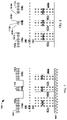
FIG. 1A is a cross sectional illustration of a semiconductor arrangement at a stage of fabrication, in accordance with one or more embodiments.
FIG. 1B is a top illustration of a semiconductor arrangement at a stage of fabrication, in accordance with one or more embodiments, where FIG. 1A is taken along line 1-1 of FIG. 1B.
FIG. 2A is a cross sectional illustration of a semiconductor arrangement at a stage of fabrication, in accordance with one or more embodiments.
FIG. 2B is a top illustration of a semiconductor arrangement at a stage of fabrication, in accordance with one or more embodiments, where FIG. 2A is taken along line 2-2 of FIG. 2B.
FIG. 3A is a cross sectional illustration of a semiconductor arrangement at a stage of fabrication, in accordance with one or more embodiments.
FIG. 3B is a top illustration of a semiconductor arrangement at a stage of fabrication, in accordance with one or more embodiments, where FIG. 3A is taken along line 3-3 of FIG. 3B.
FIG. 4A is a cross sectional illustration of a semiconductor arrangement at a stage of fabrication, in accordance with one or more embodiments.
FIG. 4B is a top illustration of a semiconductor arrangement at a stage of fabrication, in accordance with one or more embodiments, where FIG. 4A is taken along line 4-4 of FIG. 4B.
FIG. 5A is a cross sectional illustration of a semiconductor arrangement at a stage of fabrication, in accordance with one or more embodiments.
FIG. 5B is a top illustration of a semiconductor arrangement at a stage of fabrication, in accordance with one or more embodiments, where FIG. 5A is taken along line 5-5 of FIG. 5B.
FIG. 6A is a cross sectional illustration of a semiconductor arrangement at a stage of fabrication, in accordance with one or more embodiments.
FIG. 6B is a top illustration of a semiconductor arrangement at a stage of fabrication, in accordance with one or more embodiments, where FIG. 6A is taken along line 6-6 of FIG. 6B.
FIG. 7 is a cross sectional illustration of a semiconductor arrangement at a stage of fabrication, in accordance with one or more embodiments.
FIG. 8 is a cross sectional illustration of a semiconductor arrangement at a stage of fabrication, in accordance with one or more embodiments.
FIG. 9A is a cross sectional illustration of a semiconductor arrangement at a stage of fabrication, in accordance with one or more embodiments.
FIG. 9B is a top illustration of a semiconductor arrangement at a stage of fabrication, in accordance with one or more embodiments, where FIG. 9A is taken along line 9-9 of FIG. 9B.
FIG. 10A is a cross sectional illustration of a semiconductor arrangement at a stage of fabrication, in accordance with one or more embodiments.
FIG. 10B is a top illustration of a semiconductor arrangement at a stage of fabrication, in accordance with one or more embodiments, where FIG. 10A is taken along line 10-10 of FIG. 10B.
FIG. 11A is a cross sectional illustration of a semiconductor arrangement at a stage of fabrication, in accordance with one or more embodiments.
FIG. 11B is a top illustration of a semiconductor arrangement at a stage of fabrication, in accordance with one or more embodiments, where FIG. 11A is taken along line 11-11 of FIG. 11B.
FIG. 12A is a cross sectional illustration of a semiconductor arrangement at a stage of fabrication, in accordance with one or more embodiments.
FIG. 12B is a top illustration of a semiconductor arrangement at a stage of fabrication, in accordance with one or more embodiments, where FIG. 12A is taken along line 12-12 of FIG. 12B.
FIG. 13A is a cross sectional illustration of a semiconductor arrangement at a stage of fabrication, in accordance with one or more embodiments.
FIG. 13B is a top illustration of a semiconductor arrangement at a stage of fabrication, in accordance with one or more embodiments, where FIG. 13A is taken along line 13-13 of FIG. 13B.
FIG. 14A is a cross sectional illustration of a semiconductor arrangement at a stage of fabrication, in accordance with one or more embodiments.
FIG. 14B is a top illustration of a semiconductor arrangement at a stage of fabrication, in accordance with one or more embodiments, where FIG. 14A is taken along line 14-14 of FIG. 14B.
FIG. 15 is an illustration of a circuit schematic, in accordance with one or more embodiments.
FIG. 16A is a cross sectional illustration of a semiconductor arrangement at a stage of fabrication, in accordance with one or more embodiments.
FIG. 16B is a top illustration of a semiconductor arrangement at a stage of fabrication, in accordance with one or more embodiments, where FIG. 16A is taken along line 16-16 of FIG. 16B.
DETAILED DESCRIPTION
The following disclosure provides many different embodiments, or examples, for implementing different features of the provided subject matter. Specific examples of components and arrangements are described below to simplify the present disclosure. These are, of course, merely examples and are not intended to be limiting. For example, the formation of a first feature over or on a second feature in the description that follows may include embodiments in which the first and second features are formed in direct contact, and may also include embodiments in which additional features may be formed between the first and second features, such that the first and second features may not be in direct contact. In addition, the present disclosure may repeat reference numerals or letters in the various examples. This repetition is for the purpose of simplicity and clarity and does not in itself dictate a relationship between the various embodiments or configurations discussed.
Further, spatially relative terms, such as “beneath,” “below,” “lower,” “above,” “upper” and the like, may be used herein for ease of description to describe one element or feature's relationship to another element(s) or feature(s) as illustrated in the Figs. The spatially relative terms are intended to encompass different orientations of the device in use or operation in addition to the orientation depicted in the Figs. The apparatus may be otherwise oriented (rotated 90 degrees or at other orientations) and the spatially relative descriptors used herein may likewise be interpreted accordingly.
Some embodiments relate to fabricating a semiconductor arrangement. In accordance with some embodiments, the fabrication includes forming a first semiconductive layer over a first dielectric layer, patterning the first semiconductive layer to form a patterned first semiconductive layer, and patterning the first dielectric layer using the patterned first semiconductive layer to form a patterned first dielectric layer. The pattern formed in the patterned first dielectric layer is transferred to one or more underlying layers in some embodiments. According to some embodiments, a negative of the pattern formed in the patterned first dielectric layer is transferred to one or more underlying layers.
FIGS. 1A-16B illustrate a semiconductor arrangement 100 at various stages of fabrication, in accordance with some embodiments.
Referring to FIG. 1A, the semiconductor arrangement 100 is formed over a substrate 102. According to some embodiments, the substrate 102 comprises at least one of an epitaxial layer, a silicon-on-insulator (SOI) structure, a wafer, or a die formed from a wafer. According to some embodiments, one or more layers, structures, features, elements, etc. (not shown) are between the substrate 102 and the semiconductor arrangement 100.
According to some embodiments, the semiconductor arrangement 100 comprises one or more dielectric features 402 a, 402 b, 402 c, 402 d, etc. and one or more conductive features 404 a, 404 b, 404 c, etc. In some embodiments, at least some of the dielectric features comprise interlayer dielectric (ILD). In some embodiments, at least some of the dielectric features comprise at least one of tetraethylorthosilicate (TEOS), borophosphosilicate glass (BPSG), fused silica glass (FSG), phosphosilicate glass (PSG), boron doped silicon glass (BSG), or other suitable materials. In some embodiments, at least some of the conductive features comprise a gate, such as of a transistor. In some embodiments, at least some of the conductive features comprise at least one of metal, doped polysilicon, or other suitable materials.
As illustrated in FIG. 1B, where FIG. 1A is a cross sectional view taken along line 1-1 of FIG. 1B, the semiconductor arrangement 100 comprises one or more dielectric plugs 401 a 1, 401 a 2, 401 b 1, 401 c 1, 401 c 2, etc., according to some embodiments. In some embodiments, at least some of the dielectric plugs comprise at least one of oxide, nitride, or other suitable materials. In some embodiments, at least some of the dielectric plugs separate or electrically isolate portions of the conductive features from one another. In some embodiments, 401 a 1 separates 404 a 1 from 404 a 2, 401 a 2 separates 404 a 2 from 404 a 3, 401 b 1 separates 404 b 1 from 404 b 2, 401 c 1 separates 404 c 1 from 404 c 2, and 401 c 2 separates 404 c 2 from 404 c 3. In some embodiments, where one or more of the conductive features comprise gates, such as for finFET transistors, the dielectric plugs make the gates discontinuous so that some portions of the gates are not electrically coupled to other portions of the gates.
Referring to FIG. 2A and FIG. 1B, where FIG. 2A is a cross sectional view taken along line 2-2 of FIG. 2B, the semiconductor arrangement 100 comprises at least one of a first dielectric layer 104, a metal layer 106, a second dielectric layer 108, a third dielectric layer 110, or a first semiconductive layer 112 over the dielectric features 402 a, 402 b, 402 c, 402 d and the conductive features 404 a, 404 b, 404 c, according to some embodiments. In some embodiments, the first dielectric layer 104 is in direct contact with at least one of at least some of the dielectric features 402 a, 402 b, 402 c, 402 d or at least some of the conductive features 404 a, 404 b, 404 c.
According to some embodiments, the first dielectric layer 104 is an ILD layer. In some embodiments, the first dielectric layer 104 comprises at least one of tetraethylorthosilicate (TEOS), borophosphosilicate glass (BPSG), fused silica glass (FSG), phosphosilicate glass (PSG), boron doped silicon glass (BSG), or other suitable materials. In some embodiments, the first dielectric layer 104 is formed by at least one of physical vapor deposition (PVD), sputtering, chemical vapor deposition (CVD), low pressure CVD (LPCVD), atomic layer chemical vapor deposition (ALCVD), ultrahigh vacuum CVD (UHVCVD), reduced pressure CVD (RPCVD), molecular beam epitaxy (MBE), liquid phase epitaxy (LPE), or other suitable techniques.
According to some embodiments, the metal layer 106 comprises at least one of tungsten, carbide, or other suitable materials. According to some embodiments, the metal layer 106 comprises metal but has little to no electrical conductivity. According to some embodiments, the metal layer 106 is formed by at least one of PVD, sputtering, CVD, LPCVD, ALCVD, UHVCVD, RPCVD, MBE, LPE, or other suitable techniques. In some embodiments, the metal layer 106 is in direct contact with the first dielectric layer 104.
According to some embodiments, the second dielectric layer 108 comprises at least one of oxide or other suitable materials. According to some embodiments, the second dielectric layer 108 has different composition than the first dielectric layer 104. According to some embodiments, the second dielectric layer 108 has a same composition as the first dielectric layer 104. According to some embodiments, the second dielectric layer 108 is formed by at least one of PVD, sputtering, CVD, LPCVD, ALCVD, UHVCVD, RPCVD, MBE, LPE, or other suitable techniques. In some embodiments, the second dielectric layer 108 is in direct contact with the metal layer 106.
According to some embodiments, the third dielectric layer 110 comprises at least one of oxide, nitride, silicon nitride (SiN), or other suitable materials. According to some embodiments, the third dielectric layer 110 has a different composition than the first dielectric layer 104. According to some embodiments, the third dielectric layer 110 has a same composition as the first dielectric layer 104. According to some embodiments, the third dielectric layer 110 has a different composition than the second dielectric layer 108. According to some embodiments, the third dielectric layer 110 has a same composition as the second dielectric layer 108. According to some embodiments, the third dielectric layer 110 is formed by at least one of PVD, sputtering, CVD, LPCVD, ALCVD, UHVCVD, RPCVD, MBE, LPE, or other suitable techniques. In some embodiments, the third dielectric layer 110 is in direct contact with the second dielectric layer 108.
According to some embodiments, the first semiconductive layer 112 comprises at least one of silicon (Si) or other suitable materials. According to some embodiments, the first semiconductive layer 112 is formed by at least one of PVD, sputtering, CVD, LPCVD, ALCVD, UHVCVD, RPCVD, MBE, LPE, or other suitable techniques. In some embodiments, the first semiconductive layer 112 is in direct contact with the third dielectric layer 110.
Referring to FIG. 3A and FIG. 3B, where FIG. 3A is a cross sectional view taken along line 3-3 of FIG. 3B, a photoresist layer 114 is formed over the semiconductive layer 112 and patterned such that a first portion 114 a of the photoresist layer 114, a second portion 114 b of the photoresist layer 114, a third portion 114 c of the photoresist layer 114, a fourth portion 114 d of the photoresist layer 114, and a fifth portion 114 e of the photoresist layer 114 remain over the first semiconductive layer 112, according to some embodiments. According to some embodiments, the photoresist layer 114 comprises a light-sensitive material such that properties, such as solubility, of the photoresist layer 114 are affected by light. The photoresist layer 114 is either a negative photoresist or a positive photoresist. With respect to a negative photoresist, regions of the negative photoresist become insoluble when illuminated by a light source such that application of a solvent to the negative photoresist during a subsequent development stage removes non-illuminated regions of the negative photoresist. A pattern formed in the negative photoresist is thus a negative of a pattern defined by opaque regions of a template between the light source and the negative photoresist. In a positive photoresist, illuminated regions of the positive photoresist become soluble and are removed via application of a solvent during development. Thus, a pattern formed in the positive photoresist is a positive image of opaque regions of the template between the light source and the positive photoresist.
In some embodiments, the photoresist layer 114 comprises multiple layers (not shown). According to some embodiments, the photoresist layer 114 comprises three layers: a top layer, a middle layer under the top layer, and a bottom layer under the middle layer. In some embodiments, the top layer comprises a light sensitive material as described above. In some embodiments, the middle layer comprises an anti-reflective material to aid in at least one of exposure or focus of processing the light sensitive material. In some embodiments, the bottom layer comprises a hard mask material, such as at least one of nitride or other suitable materials. In some embodiments, the photoresist layer 114 is in direct contact with the first semiconductive layer 112.
FIG. 4A and FIG. 4B illustrate the pattern in the photoresist layer 114 (of FIG. 3A and FIG. 3B) transferred to the first semiconductive layer 112 to form a patterned semiconductive layer, where FIG. 4A is a cross sectional view taken along line 4-4 of FIG. 4B, such that the patterned semiconductive layer comprises a first portion 112 a of the first semiconductive layer 112, a second portion 112 b of the first semiconductive layer 112, and a third portion 112 c of the first semiconductive layer 112, according to some embodiments. According to some embodiments, an etching process is performed to pattern the first semiconductive layer 112, where the first portion 114 a (of FIG. 3A and FIG. 3B) of the photoresist layer 114 protects or shields the first portion 112 a of the first semiconductive layer 112 from an etchant applied during the etching process, the second portion 114 b (of FIG. 3A and FIG. 3B) of the photoresist layer 114 protects or shields the second portion 112 b of the first semiconductive layer 112 from the etchant applied during the etching process, and the third portion 114 c (of FIG. 3A and FIG. 3B) of the photoresist layer 114 protects or shields the third portion 112 c of the first semiconductive layer 112 from the etchant applied during the etching process. Portions of the first semiconductive layer 112 not covered by the photoresist layer 114 are exposed to the etchant and are removed or etched away during the etching process to expose portions of the third dielectric layer 110. The patterned photoresist layer 114 is then washed away, stripped, or otherwise removed. According to some embodiments, the etchant used to pattern the first semiconductive layer 112 is at least one of chlorine, hydrogen bromide, or other suitable chemicals.
As illustrated in FIG. 4A and FIG. 4B, a second photoresist layer 202 is formed over the patterned first semiconductive layer 112 a, 112 b, 112 c and exposed portions of the third dielectric layer 110, in some embodiments. According to some embodiments, the second photoresist layer 202 is patterned such that a first portion 202 a of the second photoresist layer 202 covers all of the first portion 112 a of the first semiconductive layer 112, a second portion 202 b of the second photoresist layer 202 covers all of the second portion 112 b of the first semiconductive layer 112, but a third portion 202 c of the second photoresist layer 202 covers some but not all of the third portion 112 c of the first semiconductive layer 112.
FIG. 5A and FIG. 5B illustrates the semiconductor arrangement 100 after a second etching process is performed and the patterned second photoresist layer 202 is washed away, stripped, or otherwise removed, according to some embodiments, where FIG. 5A is a cross sectional view taken along line 5-5 of FIG. 5B. Given that the first portion 202 a (of FIG. 4A) of the second photoresist layer 202 covered all of the first portion 112 a of the first semiconductive layer 112, all of the first portion 112 a of the first semiconductive layer 112 remains after the second etching process. Given that the second portion 202 b (of FIG. 4A) of the second photoresist layer 202 covered all of the second portion 112 b of the first semiconductive layer 112, all of the second portion 112 b of the first semiconductive layer 112 remains after the second etching process. FIG. 5B also illustrates a fourth portion 112 d of the first semiconductive layer 112 and a fifth portion 112 e of the first semiconductive layer 112 that remain after the first etching process and that were similarly covered and protected by the second photoresist layer 202 during the second etching process. However, given that the third portion 202 c (of FIG. 4A) of the second photoresist layer 202 covered some but not all of the third portion 112 c of the first semiconductive layer 112, merely some of the third portion 112 c of the first semiconductive layer 112 remains after the second etching process. The part of the third portion 112 c of the first semiconductive layer 112 that was not covered by the third portion 202 c of the second photoresist layer 202 is removed or etched away by an etchant that is applied during the second etching process such that the third portion 112 c of the first semiconductive layer 112 has a first cross-sectional profile before the second etching process and a second cross-sectional profile after the second etching process. According to some embodiments, a dimension, such as width, depth, etc., of the third portion 112 c of the first semiconductive layer 112 is different in the first cross-sectional profile as compared to the second cross-sectional profile. According to some embodiments, the multiple patterning actions, such as to alter the third portion 112 c of the first semiconductive layer 112 is, at times, referred to as double patterning.
According to some embodiments, portions of the third dielectric layer 110 not covered by the second photoresist layer 202 are exposed to the etchant during the second etching process such that a first recess 302 and a second recess 304 are formed in the third dielectric layer 110. In some embodiments, limitations associated with photolithography require one or more patterning operations to be performed to achieve a desired dimension, shape, etc. of a feature, such as that of the third portion 112 c of the first semiconductive layer 112 after the second etching process is performed. According to some embodiments, one or more subsequent patterning and etching operations, in addition to what is illustrated and described with regard to the patterned first photoresist layer 114 of FIG. 3A and FIG. 3B and the patterned second photoresist layer 202 of FIG. 2A and FIG. 2B, are required to achieve the desired dimension, shape, etc. of a feature. According to some embodiments, the third dielectric layer 110 is formed to have a thickness such that any recess(es) formed in the third dielectric layer 110 due to one or more patterning and etching operations do not expose the second dielectric layer 108. According to some embodiments, a lack of exposure of the second dielectric layer 108 to one or more etchants, such as O2 or a carbon-rich gas in a dry etching process, inhibits stitching in the second dielectric layer 108. According to some embodiments, stitching corresponds to one or more recesses being formed in the second dielectric layer 108, such as where the first recess 302 is transferred to the second dielectric layer 108. According to some embodiments, inhibiting the formation of one or more recesses in the second dielectric layer 108 promotes a desired composition of the second dielectric layer 108, such as by not providing a location, such as a recess, for undesired materials to be deposited or otherwise accumulate within the second dielectric layer 108. Having a desired composition of the second dielectric layer 108 promotes desired operation of a device comprising the semiconductor arrangement 100.
FIG. 6A and FIG. 6B illustrate the pattern in the patterned first semiconductive layer 112 transferred to the third dielectric layer 110 to form a patterned third dielectric layer, wherein FIG. 6A is a cross sectional view taken along line 6-6 of FIG. 6B, such that the patterned third dielectric layer comprises a first portion 110 a of the third dielectric layer 110, a second portion 110 b of the third dielectric layer 110, and a third portion 110 c of the third dielectric layer 110, according to some embodiments. According to some embodiments, an etching process is performed to pattern the third dielectric layer 110, where the first portion 112 a of the first semiconductive layer 112 protects or shields the first portion 110 a of the third dielectric layer 110 from an etchant applied during the etching process, the second portion 112 b of the first semiconductive layer 112 protects or shields the second portion 110 b of the third dielectric layer 110 from the etchant applied during the etching process, and the third portion 112 c of the first semiconductive layer 112 protects or shields the third portion 110 c of the third dielectric layer 110 from the etchant applied during the etching process. According to some embodiments, the fourth portion 112 d of the first semiconductive layer 112 protects or shields a fourth portion (not shown) of the third dielectric layer 110 and the fifth portion 112 e of the first semiconductive layer 112 protects or shields a fifth portion (not shown) of the third dielectric layer 110. Portions of the third dielectric layer 110 not covered by the first semiconductive layer 112 are exposed to the etchant and are removed or etched away during the etching process to expose portions of the second dielectric layer 108. According to some embodiments, the etchant used to etch the third dielectric layer 110 is selective such that the etchant does not etch the second dielectric layer 108. According to some embodiments, the etchant used to pattern the third dielectric layer 110 is at least one of carbon-rich gas, O2, or other suitable chemicals.
As will be appreciated from the disclosure herein, implementing the first semiconductive layer 112 facilitates forming features, elements, etc. that have desired profiles, such as substantially vertical sidewalls, according to some embodiments. By way of example, if the third dielectric layer 110 is patterned in the absence of the first semiconductive layer 112, sidewalls of the third dielectric layer 110 are tapered or not sufficiently vertical. If, for example, the third dielectric layer 110 comprises SiN and a patterned photoresist is implemented to pattern the third dielectric layer 110, an etchant used to pattern the third dielectric layer 110 also etches the patterned photoresist, such as laterally where O2 of the etchant consumes a bottom layer or portion of the photoresist. The patterned photoresist thus has at least one of a smaller dimension than desired or a tapered or non-liner sidewall, which is transferred to the third dielectric layer 110. Such etching techniques include, for example, implementing at least one of a high bias, a polymer lean gas, a carbon-rich gas, or O2. Implementing a high bias or a polymer lean gas, for example, results in stitching or undesired removal of at least one of some of the second dielectric layer 108 and thus an undesired recess in the second dielectric layer 108, where unwanted residue accumulates in the recess. Implementing a carbon-rich gas or O2, for example, in the absence of the first semiconductive layer 112 results in the aforementioned tapered profile of the photoresist and third dielectric layer 110. Implementing the first semiconductive layer 112 allows an etching process to be implemented where the first portion 110 a, the second portion 110 b, the third portion 110 c, the fourth portion, and the fifth portion of the third dielectric layer 110 have substantially vertical sidewalls. According to some embodiments, an etch selectivity of the first semiconductive layer 112 relative to an etchant, such as a carbon-rich gas or O2, allows at least one of an amount or composition of etchant to be used to etch the third dielectric layer 110 such that the first portion 110 a, the second portion 110 b, the third portion 110 c, the fourth portion, and the fifth portion of the third dielectric layer 110 have substantially vertical sidewalls, while also inhibiting unwanted side effects of the etching process. According to some embodiments, the patterned semiconductive layer 112 acts as hardmasks for the third dielectric layer 110.
FIG. 7 illustrates a fourth dielectric layer 502 formed over the first portion 112 a of the first semiconductive layer 112, the first portion 110 a of the third dielectric layer 110, the second portion 112 b of the first semiconductive layer 112, the second portion 110 b of the third dielectric layer 110, the third portion 112 c of the first semiconductive layer 112, the third portion 110 c of the third dielectric layer 110, and the second dielectric layer 108, according to some embodiments. In some embodiments, the fourth dielectric layer 502 is conformal so as to form on at least one of a sidewall of the first portion 112 a of the first semiconductive layer 112, a sidewall of the first portion 110 a of the third dielectric layer 110, a sidewall of the second portion 112 b of the first semiconductive layer 112, a sidewall of the second portion 110 b of the third dielectric layer 110, a sidewall of the third portion 112 c of the first semiconductive layer 112, or a sidewall of the third portion 110 c of the third dielectric layer 110, as well as on at least one of a top surface of the first portion 112 a of the first semiconductive layer 112, a top surface of the second portion 112 b of the first semiconductive layer 112, a top surface of the third portion 112 c of the first semiconductive layer 112, or an exposed portion of the second dielectric layer 108. According to some embodiments, the fourth dielectric layer 502 has a uniform thickness. According to some embodiments, the fourth dielectric layer 502 comprises at least one of oxide, nitride, silicon nitride (SiN), or other suitable materials. According to some embodiments, the fourth dielectric layer 502 has a different composition than the first dielectric layer 104. According to some embodiments, the fourth dielectric layer 502 has a same composition as the first dielectric layer 104. According to some embodiments, the fourth dielectric layer 502 has a different composition than the second dielectric layer 108. According to some embodiments, the fourth dielectric layer 502 has a same composition as the second dielectric layer 108. According to some embodiments, the fourth dielectric layer 502 has a different composition than the third dielectric layer 110. According to some embodiments, the fourth dielectric layer 502 has a same composition as the third dielectric layer 110. According to some embodiments, the fourth dielectric layer 502 is formed by at least one of PVD, sputtering, CVD, LPCVD, ALCVD, UHVCVD, RPCVD, MBE, LPE, or other suitable techniques. In some embodiments, the fourth dielectric layer 502 is in direct contact with at least one of the first portion 112 a of the first semiconductive layer 112, the first portion 110 a of the third dielectric layer 110, the second portion 112 b of the first semiconductive layer 112, the second portion 110 b of the third dielectric layer 110, or the second dielectric layer 108.
FIG. 8 illustrates some of the fourth dielectric layer 502 removed, according to some embodiments. In some embodiments, at least one vertical portion 502 a, 502 b, 502 c, or 502 d of the fourth dielectric layer 502 remains on at least one of a sidewall of the first portion 112 a of the first semiconductive layer 112, a sidewall of the first portion 110 a of the third dielectric layer 110, a sidewall of the second portion 112 b of the first semiconductive layer 112, a sidewall of the second portion 110 b of the third dielectric layer 110, a sidewall of the third portion 112 c of the first semiconductive layer 112, or a sidewall of the third portion 110 c of the third dielectric layer 110. According to some embodiments, an etching process is performed to remove some of the fourth dielectric layer 502. In some embodiments, the etching process comprises at least one of a plasma etching process, a reactive ion etching (RIE) process, a wet etching process, or other suitable techniques. In some embodiments, the etching process utilizes at least one of CF4, Cl2, CHF3, or other suitable materials.
Referring to FIG. 9A and FIG. 9B, where FIG. 9A is a cross sectional view taken along line 9-9 of FIG. 9B, a second semiconductive layer 702 formed over the first portion 112 a of the first semiconductive layer 112, the second portion 112 b of the first semiconductive layer 112, the third portion 112 c of the first semiconductive layer 112, the vertical portion 502 a of the fourth dielectric layer 502, the vertical portion 502 b of the fourth dielectric layer 502, the vertical portion 502 c of the fourth dielectric layer 502, the vertical portion 502 d of the fourth dielectric layer 502, and the second dielectric layer 108, according to some embodiments. According to some embodiments, the second semiconductive layer 702 comprises at least one of Si or other suitable materials. In some embodiments, the second semiconductive layer 702 has a different composition than the first semiconductive layer 112. In some embodiments, the second semiconductive layer 702 has a same composition as the first semiconductive layer 112. According to some embodiments, the second semiconductive layer 702 is formed by at least one of PVD, sputtering, CVD, LPCVD, ALCVD, UHVCVD, RPCVD, MBE, LPE, or other suitable techniques. In some embodiments, the second semiconductive layer 702 is in direct contact with at least one of the first portion 112 a of the first semiconductive layer 112, the second portion 112 b of the first semiconductive layer 112, the third portion 112 c of the first semiconductive layer 112, the vertical portion 502 a of the fourth dielectric layer 502, the vertical portion 502 b of the fourth dielectric layer 502, the vertical portion 502 c of the fourth dielectric layer 502, the vertical portion 502 d of the fourth dielectric layer 502, or the second dielectric layer 108.
Referring to FIG. 10A and FIG. 10B, where FIG. 10A is a cross sectional view taken along line 10-10 of FIG. 10B, at least some of the second semiconductive layer 702, some of the vertical portion 502 a of the fourth dielectric layer 502, some of the vertical portion 502 b of the fourth dielectric layer 502, some of the vertical portion 502 c of the fourth dielectric layer 502, some of the vertical portion 502 d of the fourth dielectric layer 502, the first portion 112 a of the first semiconductive layer 112, the second portion 112 b of the first semiconductive layer 112, and the third portion 112 c of the first semiconductive layer 112 are removed, according to some embodiments. According to some embodiments, the removal is performed by at least one of CMP or other suitable techniques. In some embodiments, an uppermost surface of at least two of remaining portion 702 a of the second semiconductive layer 702, remaining portion 702 b of the second semiconductive layer 702, remaining portion 702 c of the second semiconductive layer 702, remaining portion 702 d of the second semiconductive layer 702, the vertical portion 502 a of the fourth dielectric layer 502, the vertical portion 502 b of the fourth dielectric layer 502, the vertical portion 502 c of the fourth dielectric layer 502, the vertical portion 502 d of the fourth dielectric layer 502, the first portion 110 a of the third dielectric layer 110, the second portion 110 b of the third dielectric layer 110, the third portion 110 c of the third dielectric layer 110, a fourth portion 110 d of the third dielectric layer 110, or a fifth portion 110 e of the third dielectric layer 110 are coplanar after the removal.
Referring to FIG. 11A and FIG. 11B, where FIG. 11A is a cross sectional view taken along line 11-11 of FIG. 11B, the vertical portion 502 a of the fourth dielectric layer 502, the vertical portion 502 b of the fourth dielectric layer 502, the vertical portion 502 c of the fourth dielectric layer 502, the vertical portion 502 d of the fourth dielectric layer 502, the first portion 110 a of the third dielectric layer 110, the second portion 110 b of the third dielectric layer 110, and the third portion 110 c of the third dielectric layer 110 are removed, according to some embodiments. A patterned second semiconductive layer comprising the remaining portion 702 a of the second semiconductive layer 702, the remaining portion 702 b of the second semiconductive layer 702, the remaining portion 702 c of the second semiconductive layer 702, and the remaining portion 702 d of the second semiconductive layer 702 remains after the removal, according to some embodiments. According to some embodiments, a recess 902 a is defined between the remaining portion 702 a of the second semiconductive layer 702 and the remaining portion 702 b of the second semiconductive layer 702. According to some embodiments, a recess 902 b is defined between the remaining portions 702 a, 702 b of the second semiconductive layer 702 and the remaining portion 702 c of the second semiconductive layer 702. According to some embodiments, a recess 902 c is defined between the remaining portions 702 a, 702 b of the second semiconductive layer 702 and the remaining portion 702 d of the second semiconductive layer 702. In some embodiments, the removal is performed by an etching process. According to some embodiments, the etching process is at least one of a plasma etching process, a RIE process, a wet etching process, or other suitable techniques. In some embodiments, the etching process utilizes at least one of CF4, Cl2, CHF3, or other suitable materials. In some embodiments, one or more of the sidewalls of 702 a, 702 b, 702 c, 702 d that define the recesses are substantially vertical. In some embodiments, at least some of the aforementioned sidewalls are substantially vertical due to at least one of the selectively of the etchant of the etching process or a directionality of the etching process.
Referring to FIG. 12A and FIG. 12B, where FIG. 12A is a cross sectional view taken along line 12-12 of FIG. 12B, the pattern in the patterned second semiconductive layer 702 a, 702 b, 702 c, 702 d is transferred to the second dielectric layer 108 and the metal layer 106 to form a patterned second dielectric layer and a patterned metal layer, and the patterned second semiconductive layer is removed, according to some embodiments. According to some embodiments, the patterned second semiconductive layer 702 a, 702 b, 702 c, 702 d is removed by at least one of CMP or other suitable techniques. In some embodiments, the patterned second dielectric layer comprises a first portion 108 a of the second dielectric layer 108, a second portion 108 b of the second dielectric layer 108, a third portion 108 c of the second dielectric layer 108, and a fourth portion 108 d of the second dielectric layer 108. In some embodiments, the patterned metal layer comprises a first portion 106 a of the metal layer 106, a second portion 106 b of the metal layer 106, a third portion (not shown) of the metal layer 106, and a fourth portion (not shown) of the metal layer 106. According to some embodiments, an etching process is performed to pattern at least one of the second dielectric layer 108 or the metal layer 106, where the portions 702 a, 702 b, 702 c, 702 d of the second semiconductive layer 702 protect or shield the portions 108 a, 108 b, 108 c, 108 d of the second dielectric layer 108 from an etchant applied during the etching process. Portions of the second dielectric layer 108 not covered by the second semiconductive layer 702 are exposed to the etchant and are removed or etched away during the etching process to expose portions of the metal layer 106. Exposed portions of the metal layer 106 are then exposed to the same etchant or a different etchant(s) and removed or etched away during the etching process. According to some embodiments, a first recess 1002 a is defined between the first portion 108 a of the second dielectric layer 108 and the second portion 108 b of the second dielectric layer 108 and between the first portion 106 a of the metal layer 106 and the second portion 106 b of the metal layer 106. According to some embodiments, a second recess 1002 b is defined between the first 108 a and second 108 b portions of the second dielectric layer 108 and the third portion 108 c of the second dielectric layer 108 and between the first 106 a and second 106 b portions of the metal layer 106 and the third portion (not shown) of the metal layer 106. According to some embodiments, a third recess 1002 c is defined between the first 108 a and second 108 b portions of the second dielectric layer 108 and the fourth portion 108 d of the second dielectric layer 108 and between the first 106 a and second 106 b portions of the metal layer 106 and the fourth portion (not shown) of the metal layer 106. In some embodiments, in addition to the etching process(es) used, the substantially vertical sidewalls of 702 a, 702 b, 702 c, 702 d result in sidewalls of 108 a, 108 b, 108 c, 108 d, 106 a, 106 b, 106 c (FIG. 13B), 106 d (FIG. 13B) that define the recesses 1002 a, 1002 b, 1002 c being substantially vertical.
Referring to FIG. 13A and FIG. 13B, where FIG. 13A is a cross sectional view taken along line 13-13 of FIG. 13B, dielectric material is removed, such as the portions 108 a, 108 b, 108 c, 108 d of the second dielectric layer 108, exposed portions of the first dielectric layer 104, some of the dielectric feature 402 a, and some of the dielectric feature 402 d, according to some embodiments. According to some embodiments, such removal occurs by way of at least one of etching or other suitable techniques.
As illustrated in FIG. 13B, removal of the dielectric material exposes the first portion 106 a of the metal layer 106, the second portion 106 b of the metal layer 106, the third portion 106 c of the metal layer 106, and the fourth portion 106 d of the metal layer 106, according to some embodiments. Removal of the dielectric material exposes portions 404 a 1, 404 a 2, 404 a 3, 404 b 1, 404 b 2, 404 c 1, 404 c 2, and 404 c 3 of the conductive features that are not covered by the portions 106 a, 106 b, 106 c, 106 d of the metal layer 106, according to some embodiments. Removal of the dielectric material exposes dielectric plugs 401 a 1, 401 a 2, 401 b 1, 401 c 1, 401 c 2, according to some embodiments. Removal of the dielectric material exposes epitaxy regions 410 a 1, 410 a 2, 410 b 1, 410 b 2, 410 c 1, 410 c 2, 410 d 1, 410 d 2, according to some embodiments. In some embodiments, an epitaxy region serves as a source or a drain or as a point for electrical contact to a source or a drain of a transistor, such as a finFET transistor. According to some embodiments, a fin of a finFET transistor underlies a conductive feature, such as where the conductive feature operates as a gate of the finFET transistor. According to some embodiments, the fin also underlies or is otherwise electrically connected to first and second epitaxy regions, such as where the first epitaxy region operates as a source or as a point for electrical contact to the source of the finFET transistor and where the second epitaxy region operates as a drain or as a point for electrical contact to the drain of the finFET transistor. Removal of the dielectric material exposes portions of the dielectric features 402 a, 402 b, 402 c, 402 d not covered by at least one of the portions 106 a, 106 b, 106 c, 106 d of the metal layer 106 or the epitaxy regions 410 a 1, 410 a 2, 410 b 1, 410 b 2, 410 c 1, 410 c 2, 410 d 1, 410 d 2.
Referring to FIG. 14A and FIG. 14B, where FIG. 14A is a cross sectional view taken along line 14-14 of FIG. 14B, the portions 106 a, 106 b, 106 c, 106 d of the metal layer 106 are removed, such as by at least one of CMP or other suitable techniques, and a conductive material 405 is formed over exposed features, elements, etc., according to some embodiments. In some embodiments, the conductive material 405 is metal such as copper or other suitable materials. According to some embodiments, the conductive material 405 is formed by at least one of PVD, sputtering, CVD, LPCVD, ALCVD, UHVCVD, RPCVD, MBE, LPE, or other suitable techniques. According to some embodiments, the conducive material 405 serves to electrically connect some conductive features, elements, etc.
By way of example, and not limitation, FIG. 15 is a schematic of a static random-access memory (SRAM) circuit 450. The circuit 450 comprises four transistors M1, M2, M4, M4. Gate G3 of transistor M3 and gate G4 of transistor M4 are connected to a word line (WL). Gate G1 of transistor M1 is connected to drain D2 of transistor M2 and source S4 of transistor M4. Gate G2 of transistor M2 is connected to drain D1 of transistor M1 and source S3 of transistor M3. Drain D3 of transistor M3 is connected to bit line bar (BLB) and drain D4 of transistor M4 is connected to bit line (BL). Source S1 of transistor M1 is connected to source S2 of transistor M2.
According to some embodiments, the conductive material 405 depicted in FIG. 14A and FIG. 14B makes at least one of the connection between drain D1 of transistor M1 and source S3 of transistor M3, the connection between drain D2 of transistor M2 and source S4 of transistor M4, or the connection between source S1 of transistor M1 and source S2 of transistor M2. According to some embodiments, the conductive material 405 depicted in FIG. 14A and FIG. 14B that makes such connections is, at times, referred to as a metal drain (MD).
FIG. 14A and FIG. 14B illustrate that the conductive material 405 also electrically couples conductive features 404 a, 404 b, 404 c to one another. In some embodiments, it is desirable to decouple or electrically isolate some conductive features from one another, such as 404 a, 404 b, 404 c.
Accordingly, referring to FIG. 16A and FIG. 16B, where FIG. 16A is a cross sectional view taken along line 16-16 of FIG. 16B, some of the conductive material 405, as well as remaining portions 104 a, 104 b of the first dielectric layer 104 are removed, according to some embodiments. In some embodiments, such removal occurs by way of at least one of CMP or other suitable techniques. Given that the conductive material 405 is, at times, referred to as a metal drain, removal of some of the conductive material 405 to decouple a conductive feature from one or more other conductive features is, at times, referred to as cut metal drain (CMD). As illustrated in FIG. 16B some of the conductive material 405 remains to electrically couple certain features, such as D1 to S3, D2 to S4, and S1 to S2 in the circuit 450 in FIG. 15 , according to some embodiments. According to some embodiments, portions 405 a 1, 405 a 2, 405 a 3, 405 b 1, 405 b 2, 405 b 3, 405 b 4, 405 c 1, 405 c 2, 405 c 3, 405 c 4, 405 d 1, 405 d 2, 405 d 3 of the conductive material 405 remain. According to some embodiments, portion 405 a 2 couples epitaxy regions 410 a 1 and 410 a 2 (FIG. 13B) to one another. According to some embodiments, portion 405 d 2 couples epitaxy regions 410 d 1 and 410 d 2 (FIG. 12B) to one another.
According to some embodiments, removal of some of the conductive material 405 and remaining portions of the first dielectric layer 104 exposes portions 404 a 1, 404 a 2, 404 a 3, 404 b 1, 404 b 2, 404 c 1, 404 c 2, and 404 c 3 of the conductive features. According to some embodiments, removal of some of the conductive material 405 and remaining portions of the first dielectric layer 104 exposes portions 402 a 1, 402 a 2, 402 b 1, 402 b 2, 402 b 3, 402 c 1, 402 c 2, 402 c 3, 402 d 1, and 402 d 2 of the dielectric features. According to some embodiments, the aforementioned substantially vertical sidewalls serve to develop features, elements, etc. that have desired dimensions. By way of example, and not limitation, dimensions of 402 a 1 are sufficient to electrically isolate 405 a 1 from 405 a 2. The same is true for the dimensions of at least one of 402 a 2, 402 b 1, 402 b 2, 402 b 3, 402 c 1, 402 c 2, 402 c 3, 402 d 1, or 402 d 2 so as to be able to electrically isolate or cut conductivity between adjacent or surrounding items, such as at least two of 405 a 1, 405 a 2, 405 a 3, 405 b 1, 405 b 2, 405 b 3, 405 b 4, 405 c 1, 405 c 2, 405 c 3, 405 c 4, 405 d 1, 405 d 2, or 405 d 3, according to some embodiments.
Some embodiments described herein relate to fabricating a semiconductor arrangement. In accordance with some embodiments, the fabrication includes forming a first semiconductive layer over a first dielectric layer, patterning the first semiconductive layer to form a patterned first semiconductive layer, and patterning the first dielectric layer using the patterned first semiconductive layer to form a patterned first dielectric layer. The pattern formed in the patterned first dielectric layer is transferred to one or more underlying layers in some embodiments. According to some embodiments, a negative of the pattern formed in the patterned first dielectric layer is transferred to one or more underlying layers. According to some embodiments, the fabrication produces recesses defined by substantially vertical sidewalls. Features, elements, etc. formed in the recesses thus have substantially vertical or smooth sidewalls or profiles.
According to some embodiments, a method for fabricating a semiconductor arrangement is provided that includes forming a first dielectric layer, forming a first semiconductive layer over the first dielectric layer, patterning the first semiconductive layer to form a patterned first semiconductive layer, patterning the first dielectric layer using the patterned first semiconductive layer to form a patterned first dielectric layer, and forming a second semiconductive layer over the patterned first dielectric layer and the patterned first semiconductive layer.
According to some embodiments, a method for fabricating a semiconductor arrangement is provided that includes forming a silicon nitride layer, forming a silicon layer over the silicon nitride layer, and patterning the silicon layer to form a recess in the silicon nitride layer and a patterned silicon layer comprising a first silicon structure and a second silicon structure.
According to some embodiments, a method for fabricating a semiconductor arrangement is provided that includes forming a first dielectric layer over an oxide layer, forming a first semiconductive layer over the first dielectric layer, performing a first etch to form a first semiconductive structure and a second semiconductive structure from the first semiconductive layer, and performing a second etch to change a cross-sectional profile of the first semiconductive structure, where at least one of the first etch or the second etch forms a recess in the first dielectric layer.
The foregoing outlines features of several embodiments so that those of ordinary skill in the art may better understand various aspects of the present disclosure. Those of ordinary skill in the art should appreciate that they may readily use the present disclosure as a basis for designing or modifying other processes and structures for carrying out the same purposes or achieving the same advantages of various embodiments introduced herein. Those of ordinary skill in the art should also realize that such equivalent constructions do not depart from the spirit and scope of the present disclosure, and that they may make various changes, substitutions, and alterations herein without departing from the spirit and scope of the present disclosure.
Although the subject matter has been described in language specific to structural features or methodological acts, it is to be understood that the subject matter of the appended claims is not necessarily limited to the specific features or acts described above. Rather, the specific features and acts described above are disclosed as example forms of implementing at least some of the claims.
Various operations of embodiments are provided herein. The order in which some or all of the operations are described should not be construed to imply that these operations are necessarily order dependent. Alternative ordering will be appreciated having the benefit of this description. Further, it will be understood that not all operations are necessarily present in each embodiment provided herein. Also, it will be understood that not all operations are necessary in some embodiments.
It will be appreciated that layers, features, elements, etc. depicted herein are illustrated with particular dimensions relative to one another, such as structural dimensions or orientations, for example, for purposes of simplicity and ease of understanding and that actual dimensions of the same differ substantially from that illustrated herein, in some embodiments. Additionally, a variety of techniques exist for forming the layers, regions, features, elements, etc. mentioned herein, such as at least one of etching techniques, planarization techniques, implanting techniques, doping techniques, spin-on techniques, sputtering techniques, growth techniques, or deposition techniques such as chemical vapor deposition (CVD), for example.
Moreover, “exemplary” is used herein to mean serving as an example, instance, illustration, etc., and not necessarily as advantageous. As used in this application, “or” is intended to mean an inclusive “or” rather than an exclusive “or”. In addition, “a” and “an” as used in this application and the appended claims are generally be construed to mean “one or more” unless specified otherwise or clear from context to be directed to a singular form. Also, at least one of A and B and/or the like generally means A or B or both A and B. Furthermore, to the extent that “includes”, “having”, “has”, “with”, or variants thereof are used, such terms are intended to be inclusive in a manner similar to the term “comprising”. Also, unless specified otherwise, “first,” “second,” or the like are not intended to imply a temporal aspect, a spatial aspect, an ordering, etc. Rather, such terms are merely used as identifiers, names, etc. for features, elements, items, etc. For example, a first element and a second element generally correspond to element A and element B or two different or two identical elements or the same element.
Also, although the disclosure has been shown and described with respect to one or more implementations, equivalent alterations and modifications will occur to others of ordinary skill in the art based upon a reading and understanding of this specification and the annexed drawings. The disclosure includes all such modifications and alterations and is limited only by the scope of the following claims. In particular regard to the various functions performed by the above described components the terms used to describe such components are intended to correspond, unless otherwise indicated, to any component which performs the specified function of the described component (for example, a term that is functionally equivalent), even though not structurally equivalent to the disclosed structure. In addition, while a particular feature of the disclosure may have been disclosed with respect to only one of several implementations, such feature may be combined with one or more other features of the other implementations as may be desired and advantageous for any given or particular application.

Claims (20)

What is claimed is:
1. A method for fabricating a semiconductor arrangement, comprising:
forming a first dielectric layer;
forming a first semiconductive layer over the first dielectric layer;
patterning the first semiconductive layer to form a patterned first semiconductive layer;
patterning the first dielectric layer using the patterned first semiconductive layer to form a patterned first dielectric layer; and
forming a second semiconductive layer over the patterned first dielectric layer and the patterned first semiconductive layer.
2. The method of claim 1, wherein the first semiconductive layer and the second semiconductive layer have a same material composition.
3. The method of claim 1, wherein patterning the first semiconductive layer comprises:
performing a first etch to form a first semiconductive structure from the first semiconductive layer, wherein the first semiconductive structure has a first cross-sectional profile; and
performing a second etch to change a cross-sectional profile of the first semiconductive structure from the first cross-sectional profile to a second cross-sectional profile.
4. The method of claim 3, wherein performing at least one of the first etch or the second etch comprises etching the first dielectric layer to define a recess in the first dielectric layer.
5. The method of claim 1, wherein the first semiconductive layer is a silicon layer.
6. The method of claim 1, wherein the first dielectric layer is a silicon nitride layer.
7. The method of claim 1, comprising forming a second dielectric layer adjacent a sidewall of the patterned first semiconductive layer and adjacent a sidewall of the patterned first dielectric layer prior to forming the second semiconductive layer.
8. The method of claim 1, comprising removing the patterned first semiconductive layer after forming the second semiconductive layer to expose the patterned first dielectric layer.
9. The method of claim 8, comprising removing the patterned first dielectric layer to expose a sidewall of the second semiconductive layer.
10. The method of claim 8, comprising forming a second dielectric layer adjacent a sidewall of the patterned first semiconductive layer and adjacent a sidewall of the patterned first dielectric layer prior to forming the second semiconductive layer.
11. The method of claim 10, comprising removing the patterned first dielectric layer and the second dielectric layer to expose a sidewall of the second semiconductive layer.
12. A method for fabricating a semiconductor arrangement, comprising:
forming a silicon nitride layer;
forming a silicon layer over the silicon nitride layer;
patterning the silicon layer to form a recess in the silicon nitride layer and a patterned silicon layer comprising a first silicon structure and a second silicon structure;
removing a first portion of the silicon nitride layer between the first silicon structure and the second silicon structure to expose a first portion of an oxide layer underlying the silicon nitride layer;
forming a second silicon layer over the first portion of the oxide layer;
removing the first silicon structure to expose a second portion of the silicon nitride layer after removing the first portion of the silicon nitride layer;
removing the second portion of the silicon nitride layer to expose a second portion of the oxide layer; and
removing the second portion of the oxide layer while a portion of the second silicon layer remains over the first portion of the oxide layer.
13. A method for fabricating a semiconductor arrangement, comprising:
forming a first dielectric layer over an oxide layer;
forming a first semiconductive layer over the first dielectric layer;
performing a first etch to form a first semiconductive structure and a second semiconductive structure from the first semiconductive layer; and
performing a second etch to change a cross-sectional profile of the first semiconductive structure, wherein at least one of the first etch or the second etch forms a recess in the first dielectric layer.
14. The method of claim 1, comprising:
exposing a top surface of the first semiconductive layer after patterning the first semiconductive layer and before patterning the first dielectric layer, wherein patterning the first dielectric layer comprises patterning the first dielectric layer while the top surface of the first semiconductive layer is exposed.
15. The method of claim 12, wherein removing the first silicon structure to expose a second portion of the silicon nitride layer comprises removing the first silicon structure to expose the second portion of the silicon nitride layer after forming the second silicon layer.
16. The method of claim 12, comprising forming a dielectric layer adjacent a sidewall of the first silicon structure, wherein forming the second silicon layer comprises forming the second silicon layer such that the dielectric layer is between the sidewall of the first silicon structure and a sidewall of the second silicon layer.
17. The method of claim 16, wherein forming the dielectric layer comprises forming the dielectric layer after removing the first portion of the silicon nitride layer.
18. The method of claim 16, comprising removing the dielectric layer after forming the second silicon layer.
19. The method of claim 13, comprising performing a third etch to remove a portion of the first dielectric layer and expose a first portion of the oxide layer after performing the second etch.
20. The method of claim 19, comprising forming a second semiconductor layer over the first portion of the oxide layer after performing the third etch.
US16/689,154 2018-11-30 2019-11-20 Semiconductor arrangement and method for making Active 2040-04-10 US11587782B2 (en)

Priority Applications (4)

Application Number Priority Date Filing Date Title
US16/689,154 US11587782B2 (en) 2018-11-30 2019-11-20 Semiconductor arrangement and method for making
TW108143624A TW202109669A (en) 2018-11-30 2019-11-29 Method for fabricating semiconductor device
CN201911212801.3A CN111261510A (en) 2018-11-30 2019-12-02 Semiconductor device manufacturing method
US18/111,792 US11901176B2 (en) 2018-11-30 2023-02-20 Semiconductor arrangement and method for making

Applications Claiming Priority (2)

Application Number Priority Date Filing Date Title
US201862773335P 2018-11-30 2018-11-30
US16/689,154 US11587782B2 (en) 2018-11-30 2019-11-20 Semiconductor arrangement and method for making

Related Child Applications (1)

Application Number Title Priority Date Filing Date
US18/111,792 Continuation US11901176B2 (en) 2018-11-30 2023-02-20 Semiconductor arrangement and method for making

Publications (2)

Publication Number Publication Date
US20200176242A1 US20200176242A1 (en) 2020-06-04
US11587782B2 true US11587782B2 (en) 2023-02-21

Family

ID=70850600

Family Applications (2)

Application Number Title Priority Date Filing Date
US16/689,154 Active 2040-04-10 US11587782B2 (en) 2018-11-30 2019-11-20 Semiconductor arrangement and method for making
US18/111,792 Active US11901176B2 (en) 2018-11-30 2023-02-20 Semiconductor arrangement and method for making

Family Applications After (1)

Application Number Title Priority Date Filing Date
US18/111,792 Active US11901176B2 (en) 2018-11-30 2023-02-20 Semiconductor arrangement and method for making

Country Status (3)

Country Link
US (2) US11587782B2 (en)
CN (1) CN111261510A (en)
TW (1) TW202109669A (en)

Citations (19)

* Cited by examiner, † Cited by third party
Publication number Priority date Publication date Assignee Title
US20030148581A1 (en) * 2002-02-05 2003-08-07 Dong-Woo Kim Capacitors of semiconductor devices and methods of fabricating the same
US6680258B1 (en) * 2002-10-02 2004-01-20 Promos Technologies, Inc. Method of forming an opening through an insulating layer of a semiconductor device
US20070059891A1 (en) * 2005-09-14 2007-03-15 International Business Machines Corporation Mandrel/trim alignment in SIT processing
US20130122686A1 (en) * 2011-11-16 2013-05-16 Taiwan Semiconductor Manufacturing Company, Ltd. Reverse Tone STI Formation
US20130277759A1 (en) * 2012-04-20 2013-10-24 Taiwan Semiconductor Manufacturing Company, Ltd. Semiconductor Fin Structures and Methods for Forming the Same
US20140048884A1 (en) * 2012-08-14 2014-02-20 International Business Machines Corporation Disposable carbon-based template layer for formation of borderless contact structures
US20140312395A1 (en) * 2013-04-22 2014-10-23 International Business Machines Corporation Self-aligned borderless contacts using a photo-patternable dielectric material as a replacement contact
US20140339629A1 (en) * 2013-05-15 2014-11-20 International Business Machines Corporation Contact formation for ultra-scaled devices
US20150048455A1 (en) * 2013-08-19 2015-02-19 International Business Machines Corporation Self-aligned gate contact structure
US20150236106A1 (en) * 2014-02-20 2015-08-20 Globalfoundries Inc. Method for creating self-aligned transistor contacts
US20150243513A1 (en) * 2013-12-23 2015-08-27 International Business Machines Corporation Fin density control of multigate devices through sidewall image transfer processes
US20170170300A1 (en) * 2015-12-15 2017-06-15 Taiwan Semiconductor Manufacturing Co., Ltd. Fin field effect transistor, semiconductor device and fabricating method thereof
US20170229452A1 (en) * 2016-02-05 2017-08-10 Taiwan Semiconductor Manufacturing Co., Ltd. Fin field effect transistor and method for fabricating the same
US20170229451A1 (en) * 2016-02-05 2017-08-10 Taiwan Semiconductor Manufacturing Co., Ltd. Fin field effect transistor and method for fabricating the same
US20170316984A1 (en) * 2016-05-02 2017-11-02 Taiwan Semiconductor Manufacturing Company, Ltd. Finfet structures and methods of forming the same
US20180096846A1 (en) * 2016-10-04 2018-04-05 International Business Machines Corporation Selective gas etching for self-aligned pattern transfer
US20190148147A1 (en) * 2017-11-15 2019-05-16 Taiwan Semiconductor Manufacturing Co., Ltd. Fine line patterning methods
US20200058649A1 (en) * 2018-08-14 2020-02-20 Taiwan Semiconductor Manufacturing Co., Ltd. Semiconductor device and manufacturing method thereof
US20200111673A1 (en) * 2018-10-08 2020-04-09 Micron Technology, Inc. Methods of forming semiconductor devices using mask materials, and related semiconductor devices and systems

Family Cites Families (11)

* Cited by examiner, † Cited by third party
Publication number Priority date Publication date Assignee Title
JP4256347B2 (en) * 2003-04-30 2009-04-22 富士通マイクロエレクトロニクス株式会社 Manufacturing method of semiconductor device
US9390909B2 (en) * 2013-11-07 2016-07-12 Novellus Systems, Inc. Soft landing nanolaminates for advanced patterning
JP6061610B2 (en) * 2012-10-18 2017-01-18 ルネサスエレクトロニクス株式会社 Manufacturing method of semiconductor device
US9129906B2 (en) * 2013-12-05 2015-09-08 Taiwan Semiconductor Manufacturing Company, Ltd. Self-aligned double spacer patterning process
US9412830B2 (en) * 2014-04-17 2016-08-09 Fujitsu Limited Semiconductor device and method of manufacturing semiconductor device
CN105336571B (en) * 2014-07-28 2018-06-01 中芯国际集成电路制造(上海)有限公司 The forming method of autoregistration multiple graphics mask
US9576954B1 (en) * 2015-09-23 2017-02-21 International Business Machines Corporation POC process flow for conformal recess fill
KR102457289B1 (en) * 2017-04-25 2022-10-21 에이에스엠 아이피 홀딩 비.브이. Method for depositing a thin film and manufacturing a semiconductor device
CN109545684B (en) * 2017-09-22 2020-11-27 中芯国际集成电路制造(上海)有限公司 Semiconductor structure and method of forming the same
KR102487054B1 (en) * 2017-11-28 2023-01-13 삼성전자주식회사 Etching method and methods of manufacturing semiconductor device using the same
CN115831969A (en) * 2017-11-30 2023-03-21 英特尔公司 Fin Patterning for Fabrication of Advanced Integrated Circuit Structures

Patent Citations (22)

* Cited by examiner, † Cited by third party
Publication number Priority date Publication date Assignee Title
US20030148581A1 (en) * 2002-02-05 2003-08-07 Dong-Woo Kim Capacitors of semiconductor devices and methods of fabricating the same
US6680258B1 (en) * 2002-10-02 2004-01-20 Promos Technologies, Inc. Method of forming an opening through an insulating layer of a semiconductor device
US20070059891A1 (en) * 2005-09-14 2007-03-15 International Business Machines Corporation Mandrel/trim alignment in SIT processing
US20130122686A1 (en) * 2011-11-16 2013-05-16 Taiwan Semiconductor Manufacturing Company, Ltd. Reverse Tone STI Formation
US20140099779A1 (en) * 2011-11-16 2014-04-10 Taiwan Semiconductor Manufacturing Company, Ltd. Reverse Tone STI Formation
US20140099771A1 (en) * 2011-11-16 2014-04-10 Taiwan Semiconductor Manufacturing Company, Ltd. Reverse Tone STI Formation
US20170229348A1 (en) * 2012-04-20 2017-08-10 Taiwan Semiconductor Manufacturing Company, Ltd. Methods for Forming Fin Field-Effect Transistors
US20130277759A1 (en) * 2012-04-20 2013-10-24 Taiwan Semiconductor Manufacturing Company, Ltd. Semiconductor Fin Structures and Methods for Forming the Same
US20140048884A1 (en) * 2012-08-14 2014-02-20 International Business Machines Corporation Disposable carbon-based template layer for formation of borderless contact structures
US20140312395A1 (en) * 2013-04-22 2014-10-23 International Business Machines Corporation Self-aligned borderless contacts using a photo-patternable dielectric material as a replacement contact
US20140339629A1 (en) * 2013-05-15 2014-11-20 International Business Machines Corporation Contact formation for ultra-scaled devices
US20150048455A1 (en) * 2013-08-19 2015-02-19 International Business Machines Corporation Self-aligned gate contact structure
US20150243513A1 (en) * 2013-12-23 2015-08-27 International Business Machines Corporation Fin density control of multigate devices through sidewall image transfer processes
US20150236106A1 (en) * 2014-02-20 2015-08-20 Globalfoundries Inc. Method for creating self-aligned transistor contacts
US20170170300A1 (en) * 2015-12-15 2017-06-15 Taiwan Semiconductor Manufacturing Co., Ltd. Fin field effect transistor, semiconductor device and fabricating method thereof
US20170229452A1 (en) * 2016-02-05 2017-08-10 Taiwan Semiconductor Manufacturing Co., Ltd. Fin field effect transistor and method for fabricating the same
US20170229451A1 (en) * 2016-02-05 2017-08-10 Taiwan Semiconductor Manufacturing Co., Ltd. Fin field effect transistor and method for fabricating the same
US20170316984A1 (en) * 2016-05-02 2017-11-02 Taiwan Semiconductor Manufacturing Company, Ltd. Finfet structures and methods of forming the same
US20180096846A1 (en) * 2016-10-04 2018-04-05 International Business Machines Corporation Selective gas etching for self-aligned pattern transfer
US20190148147A1 (en) * 2017-11-15 2019-05-16 Taiwan Semiconductor Manufacturing Co., Ltd. Fine line patterning methods
US20200058649A1 (en) * 2018-08-14 2020-02-20 Taiwan Semiconductor Manufacturing Co., Ltd. Semiconductor device and manufacturing method thereof
US20200111673A1 (en) * 2018-10-08 2020-04-09 Micron Technology, Inc. Methods of forming semiconductor devices using mask materials, and related semiconductor devices and systems

Also Published As

Publication number Publication date
US11901176B2 (en) 2024-02-13
US20200176242A1 (en) 2020-06-04
CN111261510A (en) 2020-06-09
TW202109669A (en) 2021-03-01
US20230197439A1 (en) 2023-06-22

Similar Documents

Publication Publication Date Title
US12471310B2 (en) Method of making a FinFET device including a step of removing a portion of a fin
US8969974B2 (en) Structure and method for FinFET device
US11640924B2 (en) Structure and method for interconnection with self-alignment
US10868184B2 (en) Fin field effect transistor (FinFET) device structure with hard mask layer over gate structure and method for forming the same
US11854965B2 (en) Sidewall spacer structure enclosing conductive wire sidewalls to increase reliability
US10672648B2 (en) Method of forming semiconductor memory device
US20240387357A1 (en) Semiconductor interconnect structure with bottom self-aligned via landing
US6528418B1 (en) Manufacturing method for semiconductor device
US11769672B2 (en) Semiconductor structure and forming method thereof
US10079172B2 (en) Wiring structure and method of forming a wiring structure
US6566236B1 (en) Gate structures with increased etch margin for self-aligned contact and the method of forming the same
US10685871B2 (en) Method for forming semiconductor structure
US11901176B2 (en) Semiconductor arrangement and method for making
TWI651764B (en) Apparatus and method for forming a cross-coupled contact
US8318556B2 (en) Method and system for continuous line-type landing polysilicon contact (LPC) structures
US10727136B2 (en) Integrated gate contact and cross-coupling contact formation
US6979651B1 (en) Method for forming alignment features and back-side contacts with fewer lithography and etch steps
US20190371905A1 (en) Semiconductor device with reduced gate height budget
US12142519B2 (en) Etch stop detection structure and etch stop detection method
US11651964B2 (en) Semiconductor structure and forming method thereof
US11538686B2 (en) Semiconductor structure and method for forming the same
US12495598B2 (en) Semiconductor device and manufacturing method thereof
US10008408B2 (en) Devices and methods of forming asymmetric line/space with barrierless metallization
US12074059B2 (en) Semiconductor arrangement and method of making
US12176212B2 (en) Mandrel structures and methods of fabricating the same in semiconductor devices

Legal Events

Date Code Title Description
FEPP Fee payment procedure

Free format text: ENTITY STATUS SET TO UNDISCOUNTED (ORIGINAL EVENT CODE: BIG.); ENTITY STATUS OF PATENT OWNER: LARGE ENTITY

STPP Information on status: patent application and granting procedure in general

Free format text: NON FINAL ACTION MAILED

STPP Information on status: patent application and granting procedure in general

Free format text: RESPONSE TO NON-FINAL OFFICE ACTION ENTERED AND FORWARDED TO EXAMINER

STPP Information on status: patent application and granting procedure in general

Free format text: NON FINAL ACTION MAILED

STPP Information on status: patent application and granting procedure in general

Free format text: RESPONSE TO NON-FINAL OFFICE ACTION ENTERED AND FORWARDED TO EXAMINER

STPP Information on status: patent application and granting procedure in general

Free format text: NON FINAL ACTION MAILED

STPP Information on status: patent application and granting procedure in general

Free format text: RESPONSE TO NON-FINAL OFFICE ACTION ENTERED AND FORWARDED TO EXAMINER

STPP Information on status: patent application and granting procedure in general

Free format text: FINAL REJECTION MAILED

STPP Information on status: patent application and granting procedure in general

Free format text: RESPONSE AFTER FINAL ACTION FORWARDED TO EXAMINER

STPP Information on status: patent application and granting procedure in general

Free format text: NOTICE OF ALLOWANCE MAILED -- APPLICATION RECEIVED IN OFFICE OF PUBLICATIONS

STCF Information on status: patent grant

Free format text: PATENTED CASE