US11574975B2 - Light emitting diode display device with channel region covered by drain electrode - Google Patents
Light emitting diode display device with channel region covered by drain electrode Download PDFInfo
- Publication number
- US11574975B2 US11574975B2 US16/882,260 US202016882260A US11574975B2 US 11574975 B2 US11574975 B2 US 11574975B2 US 202016882260 A US202016882260 A US 202016882260A US 11574975 B2 US11574975 B2 US 11574975B2
- Authority
- US
- United States
- Prior art keywords
- light emitting
- emitting diode
- display device
- slit
- semiconductor
- Prior art date
- Legal status (The legal status is an assumption and is not a legal conclusion. Google has not performed a legal analysis and makes no representation as to the accuracy of the status listed.)
- Active
Links
- 239000010410 layer Substances 0.000 claims abstract description 297
- 239000004065 semiconductor Substances 0.000 claims abstract description 180
- 239000000758 substrate Substances 0.000 claims abstract description 116
- 239000011229 interlayer Substances 0.000 claims abstract description 67
- 239000004020 conductor Substances 0.000 claims description 11
- 239000010409 thin film Substances 0.000 description 51
- 239000003990 capacitor Substances 0.000 description 39
- 239000000463 material Substances 0.000 description 31
- 238000002161 passivation Methods 0.000 description 23
- 239000007769 metal material Substances 0.000 description 17
- PQXKHYXIUOZZFA-UHFFFAOYSA-M lithium fluoride Chemical compound [Li+].[F-] PQXKHYXIUOZZFA-UHFFFAOYSA-M 0.000 description 16
- 229910052751 metal Inorganic materials 0.000 description 15
- 239000002184 metal Substances 0.000 description 15
- VYPSYNLAJGMNEJ-UHFFFAOYSA-N silicon dioxide Inorganic materials O=[Si]=O VYPSYNLAJGMNEJ-UHFFFAOYSA-N 0.000 description 15
- 230000000903 blocking effect Effects 0.000 description 13
- TWNQGVIAIRXVLR-UHFFFAOYSA-N oxo(oxoalumanyloxy)alumane Chemical compound O=[Al]O[Al]=O TWNQGVIAIRXVLR-UHFFFAOYSA-N 0.000 description 12
- 229910052814 silicon oxide Inorganic materials 0.000 description 12
- 239000011810 insulating material Substances 0.000 description 11
- 239000011575 calcium Substances 0.000 description 8
- 229910052581 Si3N4 Inorganic materials 0.000 description 6
- XUIMIQQOPSSXEZ-UHFFFAOYSA-N Silicon Chemical compound [Si] XUIMIQQOPSSXEZ-UHFFFAOYSA-N 0.000 description 6
- OJCDKHXKHLJDOT-UHFFFAOYSA-N fluoro hypofluorite;silicon Chemical compound [Si].FOF OJCDKHXKHLJDOT-UHFFFAOYSA-N 0.000 description 6
- 229910052710 silicon Inorganic materials 0.000 description 6
- 239000010703 silicon Substances 0.000 description 6
- HQVNEWCFYHHQES-UHFFFAOYSA-N silicon nitride Chemical compound N12[Si]34N5[Si]62N3[Si]51N64 HQVNEWCFYHHQES-UHFFFAOYSA-N 0.000 description 6
- 239000002356 single layer Substances 0.000 description 6
- 238000002834 transmittance Methods 0.000 description 6
- 239000012535 impurity Substances 0.000 description 5
- OYPRJOBELJOOCE-UHFFFAOYSA-N Calcium Chemical compound [Ca] OYPRJOBELJOOCE-UHFFFAOYSA-N 0.000 description 4
- 229910052782 aluminium Inorganic materials 0.000 description 4
- XAGFODPZIPBFFR-UHFFFAOYSA-N aluminium Chemical compound [Al] XAGFODPZIPBFFR-UHFFFAOYSA-N 0.000 description 4
- 229910052791 calcium Inorganic materials 0.000 description 4
- 239000010931 gold Substances 0.000 description 4
- 229910003437 indium oxide Inorganic materials 0.000 description 4
- PJXISJQVUVHSOJ-UHFFFAOYSA-N indium(iii) oxide Chemical compound [O-2].[O-2].[O-2].[In+3].[In+3] PJXISJQVUVHSOJ-UHFFFAOYSA-N 0.000 description 4
- 238000002347 injection Methods 0.000 description 4
- 239000007924 injection Substances 0.000 description 4
- 239000011777 magnesium Substances 0.000 description 4
- 239000012780 transparent material Substances 0.000 description 4
- XLOMVQKBTHCTTD-UHFFFAOYSA-N Zinc monoxide Chemical compound [Zn]=O XLOMVQKBTHCTTD-UHFFFAOYSA-N 0.000 description 3
- 230000002093 peripheral effect Effects 0.000 description 3
- -1 region Substances 0.000 description 3
- 239000011347 resin Substances 0.000 description 3
- 229920005989 resin Polymers 0.000 description 3
- 239000004925 Acrylic resin Substances 0.000 description 2
- WHXSMMKQMYFTQS-UHFFFAOYSA-N Lithium Chemical compound [Li] WHXSMMKQMYFTQS-UHFFFAOYSA-N 0.000 description 2
- FYYHWMGAXLPEAU-UHFFFAOYSA-N Magnesium Chemical compound [Mg] FYYHWMGAXLPEAU-UHFFFAOYSA-N 0.000 description 2
- BQCADISMDOOEFD-UHFFFAOYSA-N Silver Chemical compound [Ag] BQCADISMDOOEFD-UHFFFAOYSA-N 0.000 description 2
- UMIVXZPTRXBADB-UHFFFAOYSA-N benzocyclobutene Chemical compound C1=CC=C2CCC2=C1 UMIVXZPTRXBADB-UHFFFAOYSA-N 0.000 description 2
- 238000000151 deposition Methods 0.000 description 2
- 239000010408 film Substances 0.000 description 2
- PCHJSUWPFVWCPO-UHFFFAOYSA-N gold Chemical compound [Au] PCHJSUWPFVWCPO-UHFFFAOYSA-N 0.000 description 2
- 229910052737 gold Inorganic materials 0.000 description 2
- AMGQUBHHOARCQH-UHFFFAOYSA-N indium;oxotin Chemical compound [In].[Sn]=O AMGQUBHHOARCQH-UHFFFAOYSA-N 0.000 description 2
- 229910010272 inorganic material Inorganic materials 0.000 description 2
- 239000011147 inorganic material Substances 0.000 description 2
- 229910052744 lithium Inorganic materials 0.000 description 2
- 229910052749 magnesium Inorganic materials 0.000 description 2
- 229920001721 polyimide Polymers 0.000 description 2
- 239000009719 polyimide resin Substances 0.000 description 2
- 229910052709 silver Inorganic materials 0.000 description 2
- 239000004332 silver Substances 0.000 description 2
- YVTHLONGBIQYBO-UHFFFAOYSA-N zinc indium(3+) oxygen(2-) Chemical compound [O--].[Zn++].[In+3] YVTHLONGBIQYBO-UHFFFAOYSA-N 0.000 description 2
- KXGFMDJXCMQABM-UHFFFAOYSA-N 2-methoxy-6-methylphenol Chemical compound [CH]OC1=CC=CC([CH])=C1O KXGFMDJXCMQABM-UHFFFAOYSA-N 0.000 description 1
- 229920000265 Polyparaphenylene Polymers 0.000 description 1
- 239000004734 Polyphenylene sulfide Substances 0.000 description 1
- 239000000919 ceramic Substances 0.000 description 1
- 230000008021 deposition Effects 0.000 description 1
- 239000003989 dielectric material Substances 0.000 description 1
- 230000009977 dual effect Effects 0.000 description 1
- 239000003822 epoxy resin Substances 0.000 description 1
- 230000005281 excited state Effects 0.000 description 1
- 230000007717 exclusion Effects 0.000 description 1
- 239000011521 glass Substances 0.000 description 1
- 230000005283 ground state Effects 0.000 description 1
- 238000010030 laminating Methods 0.000 description 1
- 239000011159 matrix material Substances 0.000 description 1
- 230000004048 modification Effects 0.000 description 1
- 238000012986 modification Methods 0.000 description 1
- 229920001568 phenolic resin Polymers 0.000 description 1
- 239000005011 phenolic resin Substances 0.000 description 1
- 239000004033 plastic Substances 0.000 description 1
- 229920006122 polyamide resin Polymers 0.000 description 1
- 229920000647 polyepoxide Polymers 0.000 description 1
- 229920000069 polyphenylene sulfide Polymers 0.000 description 1
- 239000010453 quartz Substances 0.000 description 1
- 239000000377 silicon dioxide Substances 0.000 description 1
- 229910001220 stainless steel Inorganic materials 0.000 description 1
- 239000010935 stainless steel Substances 0.000 description 1
- 230000007704 transition Effects 0.000 description 1
- 229920006337 unsaturated polyester resin Polymers 0.000 description 1
- TYHJXGDMRRJCRY-UHFFFAOYSA-N zinc indium(3+) oxygen(2-) tin(4+) Chemical compound [O-2].[Zn+2].[Sn+4].[In+3] TYHJXGDMRRJCRY-UHFFFAOYSA-N 0.000 description 1
- 239000011787 zinc oxide Substances 0.000 description 1
Images


Classifications
-
- H—ELECTRICITY
- H10—SEMICONDUCTOR DEVICES; ELECTRIC SOLID-STATE DEVICES NOT OTHERWISE PROVIDED FOR
- H10K—ORGANIC ELECTRIC SOLID-STATE DEVICES
- H10K59/00—Integrated devices, or assemblies of multiple devices, comprising at least one organic light-emitting element covered by group H10K50/00
- H10K59/10—OLED displays
- H10K59/12—Active-matrix OLED [AMOLED] displays
- H10K59/126—Shielding, e.g. light-blocking means over the TFTs
-
- H01L27/3262—
-
- H01L27/32—
-
- H01L27/3244—
-
- H01L27/3246—
-
- H01L27/3248—
-
- H01L27/3272—
-
- H01L27/3276—
-
- H01L27/3288—
-
- H—ELECTRICITY
- H01—ELECTRIC ELEMENTS
- H01L—SEMICONDUCTOR DEVICES NOT COVERED BY CLASS H10
- H01L29/00—Semiconductor devices adapted for rectifying, amplifying, oscillating or switching, or capacitors or resistors with at least one potential-jump barrier or surface barrier, e.g. PN junction depletion layer or carrier concentration layer; Details of semiconductor bodies or of electrodes thereof ; Multistep manufacturing processes therefor
- H01L29/66—Types of semiconductor device ; Multistep manufacturing processes therefor
- H01L29/68—Types of semiconductor device ; Multistep manufacturing processes therefor controllable by only the electric current supplied, or only the electric potential applied, to an electrode which does not carry the current to be rectified, amplified or switched
- H01L29/76—Unipolar devices, e.g. field effect transistors
- H01L29/772—Field effect transistors
- H01L29/78—Field effect transistors with field effect produced by an insulated gate
- H01L29/786—Thin film transistors, i.e. transistors with a channel being at least partly a thin film
- H01L29/78606—Thin film transistors, i.e. transistors with a channel being at least partly a thin film with supplementary region or layer in the thin film or in the insulated bulk substrate supporting it for controlling or increasing the safety of the device
- H01L29/78633—Thin film transistors, i.e. transistors with a channel being at least partly a thin film with supplementary region or layer in the thin film or in the insulated bulk substrate supporting it for controlling or increasing the safety of the device with a light shield
-
- H—ELECTRICITY
- H10—SEMICONDUCTOR DEVICES; ELECTRIC SOLID-STATE DEVICES NOT OTHERWISE PROVIDED FOR
- H10K—ORGANIC ELECTRIC SOLID-STATE DEVICES
- H10K59/00—Integrated devices, or assemblies of multiple devices, comprising at least one organic light-emitting element covered by group H10K50/00
-
- H—ELECTRICITY
- H10—SEMICONDUCTOR DEVICES; ELECTRIC SOLID-STATE DEVICES NOT OTHERWISE PROVIDED FOR
- H10K—ORGANIC ELECTRIC SOLID-STATE DEVICES
- H10K59/00—Integrated devices, or assemblies of multiple devices, comprising at least one organic light-emitting element covered by group H10K50/00
- H10K59/10—OLED displays
- H10K59/12—Active-matrix OLED [AMOLED] displays
- H10K59/121—Active-matrix OLED [AMOLED] displays characterised by the geometry or disposition of pixel elements
- H10K59/1213—Active-matrix OLED [AMOLED] displays characterised by the geometry or disposition of pixel elements the pixel elements being TFTs
-
- H—ELECTRICITY
- H10—SEMICONDUCTOR DEVICES; ELECTRIC SOLID-STATE DEVICES NOT OTHERWISE PROVIDED FOR
- H10K—ORGANIC ELECTRIC SOLID-STATE DEVICES
- H10K59/00—Integrated devices, or assemblies of multiple devices, comprising at least one organic light-emitting element covered by group H10K50/00
- H10K59/10—OLED displays
- H10K59/12—Active-matrix OLED [AMOLED] displays
- H10K59/122—Pixel-defining structures or layers, e.g. banks
-
- H—ELECTRICITY
- H10—SEMICONDUCTOR DEVICES; ELECTRIC SOLID-STATE DEVICES NOT OTHERWISE PROVIDED FOR
- H10K—ORGANIC ELECTRIC SOLID-STATE DEVICES
- H10K59/00—Integrated devices, or assemblies of multiple devices, comprising at least one organic light-emitting element covered by group H10K50/00
- H10K59/10—OLED displays
- H10K59/12—Active-matrix OLED [AMOLED] displays
- H10K59/123—Connection of the pixel electrodes to the thin film transistors [TFT]
-
- H—ELECTRICITY
- H10—SEMICONDUCTOR DEVICES; ELECTRIC SOLID-STATE DEVICES NOT OTHERWISE PROVIDED FOR
- H10K—ORGANIC ELECTRIC SOLID-STATE DEVICES
- H10K59/00—Integrated devices, or assemblies of multiple devices, comprising at least one organic light-emitting element covered by group H10K50/00
- H10K59/10—OLED displays
- H10K59/12—Active-matrix OLED [AMOLED] displays
- H10K59/124—Insulating layers formed between TFT elements and OLED elements
-
- H—ELECTRICITY
- H10—SEMICONDUCTOR DEVICES; ELECTRIC SOLID-STATE DEVICES NOT OTHERWISE PROVIDED FOR
- H10K—ORGANIC ELECTRIC SOLID-STATE DEVICES
- H10K59/00—Integrated devices, or assemblies of multiple devices, comprising at least one organic light-emitting element covered by group H10K50/00
- H10K59/10—OLED displays
- H10K59/12—Active-matrix OLED [AMOLED] displays
- H10K59/131—Interconnections, e.g. wiring lines or terminals
-
- H—ELECTRICITY
- H10—SEMICONDUCTOR DEVICES; ELECTRIC SOLID-STATE DEVICES NOT OTHERWISE PROVIDED FOR
- H10K—ORGANIC ELECTRIC SOLID-STATE DEVICES
- H10K59/00—Integrated devices, or assemblies of multiple devices, comprising at least one organic light-emitting element covered by group H10K50/00
- H10K59/10—OLED displays
- H10K59/17—Passive-matrix OLED displays
- H10K59/179—Interconnections, e.g. wiring lines or terminals
-
- H—ELECTRICITY
- H10—SEMICONDUCTOR DEVICES; ELECTRIC SOLID-STATE DEVICES NOT OTHERWISE PROVIDED FOR
- H10K—ORGANIC ELECTRIC SOLID-STATE DEVICES
- H10K59/00—Integrated devices, or assemblies of multiple devices, comprising at least one organic light-emitting element covered by group H10K50/00
- H10K59/80—Constructional details
- H10K59/87—Passivation; Containers; Encapsulations
Definitions
- the present disclosure relates to a light emitting diode display device.
- a light emitting diode display device includes two electrodes and an emission layer interposed therebetween. Electrons injected from one electrode and holes injected from the other electrode are combined in the emission layer to generate excitons. When the generated excitons transition to a ground state from an excited state, they release energy in the form of emitted light.
- the light emitting diode display device includes a plurality of pixels including a light emitting diode (LED) as a self-emissive element, and a plurality of transistors for driving the light emitting diode (LED) and at least one capacitor are formed in each pixel.
- the plurality of thin film transistors generally include a switching transistor and a driving transistor.
- the thin film transistor includes a gate electrode, a semiconductor, a source electrode, and a drain electrode.
- the semiconductor may absorb some of the light incident thereon, such that characteristics of the thin film transistor may be changed. For example, when the semiconductor is made of an oxide semiconductor material, visible light in a region of a short wavelength, e.g., shorter than about 387 nm, may be absorbed in the semiconductor, and thus a threshold voltage thereof may decrease.
- the light emitted from the light emitting diode (LED) is directed to an upper surface thereof, some of the emitted light is directed to a lateral surface thereof and, as such, may reach the thin film transistor positioned below the light emitting diode (LED). When this happens, the light incident on the semiconductor of the thin film transistor may cause the reliability of the thin film transistor to deteriorate.
- the described technology has been made in an effort to provide a light emitting diode display device that may improve reliability thereof by blocking light incident on a semiconductor of a thin film transistor.
- An exemplary embodiment provides a light emitting diode display device, including: a substrate; a semiconductor disposed on the substrate; a gate electrode disposed on the semiconductor; an interlayer insulating layer disposed on the substrate and the gate electrode; source and drain electrodes disposed on the interlayer insulating layer and connected to the semiconductor; a first slit provided in the interlayer insulating layer; and a first wire positioned on the interlayer insulating layer and configured to overlap the first slit.
- the first wire may contact the substrate through the first slit.
- the first wire may be disposed at the same layer as the source electrode and the drain electrode, and may be made of the same material as that of the source electrode and the drain electrode.
- the first wire may be a common voltage line.
- the first wire may be a driving voltage line connected to the source electrode.
- the first wire may be disposed at the same layer as the source electrode and the drain electrode, and may be made of the same material as that of the source electrode and the drain electrode.
- the first wire may be a common voltage line.
- the first wire may be connected to the source electrode.
- the first slit may be adjacent to an edge of one side of the semiconductor, and may not overlap the semiconductor.
- the first slit may have a bar shape extending in a first direction.
- the first slit may extend in a direction parallel to the first wire.
- the first slit may have a bar shape extending in a direction parallel to the first wire.
- the drain electrode may have an island shape.
- the semiconductor may include a channel region and a contact doping region positioned at opposite sides of the channel region, and the channel region may be covered by the drain electrode.
- the light emitting diode display device may further include a second slit provided in the interlayer insulating layer, wherein the drain electrode overlaps the second slit.
- the drain electrode may contact the substrate through the second slit.
- the second slit may be adjacent to an edge of one side of the semiconductor, and may not overlap the semiconductor.
- the second slit may extend in a direction crossing a direction in which the first wire extends.
- the light emitting diode display device may further include a first electrode connected to the drain electrode, and a passivation layer disposed between the drain electrode and the first electrode, wherein the passivation layer may be made of a light blocking material.
- the light emitting diode display device may further include a pixel defining layer configured to overlap an edge of the first electrode, wherein the pixel defining layer may be made of a light blocking material.
- the light emitting diode display device may further include a first electrode connected to the drain electrode, and a pixel defining layer configured to overlap an edge of the first electrode, wherein the pixel defining layer may be made of a light blocking material.
- the light emitting diode display device may further include a buffer layer disposed between the substrate and the interlayer insulating layer, wherein the first slit may be provided in the buffer layer and the interlayer insulating layer.
- the light emitting diode display device may further include a buffer layer disposed between the substrate and the interlayer insulating layer, wherein the first wire may contact the buffer layer through the first slit.
- the light emitting diode display device may further include a third slit provided in the interlayer insulating layer, and a second wire positioned on the interlayer insulating layer and configured to overlap the third slit.
- the second wire may be connected to the substrate through the third slit.
- the light emitting diode display device may further include a buffer layer disposed between the substrate and the interlayer insulating layer, wherein the second wire may contact the buffer layer through the third slit.
- the light emitting diode display device may further include a gate insulating layer disposed between the substrate and the gate electrode, and a fourth slit provided in the gate insulating layer, wherein the gate electrode may overlap the fourth slit.
- the gate electrode may be connected to the substrate through the fourth slit.
- the light emitting diode display device may further include a buffer layer disposed between the substrate and the gate insulating layer, wherein the gate electrode may contact the buffer layer through the fourth slit.
- the light emitting diode display device may further include a first electrode connected to the drain electrode, wherein the first electrode may cover most of the semiconductor.
- the first electrode may cover all of the semiconductor, the source electrode, the drain electrode, the gate electrode, and the first wire.
- a light emitting diode display device including: a substrate; a semiconductor disposed on the substrate; source and drain electrodes connected to the semiconductor; a gate electrode disposed on the semiconductor; a gate insulating layer disposed between the substrate and the gate electrode; and a first slit provided in the gate insulating layer, and configured to overlap the gate electrode.
- the gate electrode may contact the substrate through the first slit.
- the first slit may be adjacent to an edge of one side of the semiconductor, and may not overlap the semiconductor.
- the first slit may have a bar shape extending in a first direction.
- the light emitting diode display device may further include an interlayer insulating layer disposed between the substrate and the drain electrode, and a second slit provided in the interlayer insulating layer, wherein the drain electrode may overlap the second slit.
- the drain electrode may contact the substrate through the second slit.
- the second slit may be adjacent to an edge of one side of the semiconductor, and may not overlap the semiconductor.
- the second slit may have a bar shape extending in a direction crossing the direction in which the first slit extends.
- the light emitting diode display device may further include a buffer layer disposed between the substrate and the gate insulating layer, wherein the gate electrode contacts the buffer layer through the first slit.
- FIG. 1 illustrates a layout view of a light emitting diode display device according to an exemplary embodiment.
- FIG. 2 illustrates a cross-sectional view taken along line II-II of FIG. 1 .
- FIG. 3 illustrates a cross-sectional view taken along line III-III of FIG. 1 .
- FIG. 4 illustrates a transmittance graph according to materials of a passivation layer and a pixel defining layer.
- FIG. 5 and FIG. 6 illustrate cross-sectional views of a light emitting diode display device according to an exemplary embodiment.
- FIG. 7 illustrates a layout view of a light emitting diode display device according to an exemplary embodiment.
- FIG. 8 illustrates a cross-sectional view taken along line VIII-VIII of FIG. 7 .
- FIG. 9 illustrates a cross-sectional view of a light emitting diode display device according to an exemplary embodiment.
- FIG. 10 illustrates a layout view of a light emitting diode display device according to an exemplary embodiment.
- FIG. 11 illustrates a cross-sectional view taken along line XI-XI of FIG. 10 .
- FIG. 12 illustrates a cross-sectional view of a light emitting diode display device according to an exemplary embodiment.
- FIG. 13 illustrates a layout view of a light emitting diode display device according to an exemplary embodiment.
- FIG. 14 illustrates a cross-sectional view taken along line XIV-XIV of FIG. 13 .
- FIG. 15 illustrates a cross-sectional view of a light emitting diode display device according to an exemplary embodiment.
- FIG. 16 illustrates a layout view of a light emitting diode display device according to an exemplary embodiment.
- FIG. 17 illustrates a layout view of a light emitting diode display device according to an exemplary embodiment.
- FIG. 18 illustrates a schematic view of a light emitting diode display device according to an exemplary embodiment.
- FIG. 19 illustrates a layout view of a thin film transistor included in a gate driver of a light emitting diode display device according to an exemplary embodiment.
- FIG. 20 illustrates a cross-sectional view taken along line XX-XX of FIG. 19 .
- FIG. 21 illustrates a cross-sectional view taken along line XXI-XXI of FIG. 19 .
- the phrase “on a plane” means viewing the object portion from the top
- the phrase “on a cross-section” means viewing a cross-section of which the object portion is vertically cut from the side.
- a light emitting diode display device will be described with reference to FIG. 1 to FIG. 3 .
- FIG. 1 illustrates a layout view of a light emitting diode display device according to an exemplary embodiment
- FIG. 2 illustrates a cross-sectional view taken along line II-II of FIG. 1
- FIG. 3 illustrates a cross-sectional view taken along line III-III of FIG. 1 .
- a buffer layer 120 is positioned on a substrate 110 .
- the substrate 110 may be an insulating substrate made of glass, quartz, ceramic, plastic, etc., or a metal substrate made of stainless steel and the like.
- the buffer layer 120 may include an inorganic or organic insulating material such as a silicon oxide (SiOx), a silicon nitride (SiNx), silicon oxynitride (SiON), silicon oxyfluoride (SiOF), an aluminum oxide (AlOx), etc., and it may be formed as a single layer or a multilayer including at least one of the materials.
- the buffer layer 120 serves to flatten a surface while preventing undesirable materials, such as impurities or moisture, from permeating.
- the buffer layer 120 may be positioned on most of a region of the substrate 110 .
- the buffer layer 120 may be omitted in some cases.
- a semiconductor 135 is positioned on the buffer layer 120 .
- the semiconductor 135 may be made of a polycrystalline semiconductor material or an oxide semiconductor material.
- the semiconductor 135 includes a channel region 131 , and contact doping regions 132 and 133 that are positioned at opposite sides of the channel region 131 and include impurities such as P-type impurities or N-type impurities.
- the contact doping regions 132 and 133 include a source region 132 and a drain region 133 .
- the doped impurities may vary depending on a kind of the thin film transistor.
- a gate insulating layer 140 is positioned on the semiconductor 135 and the buffer layer 120 .
- the gate insulating layer 140 may include an inorganic insulating material or an organic insulating material such as a silicon oxide (SiOx), a silicon nitride (SiNx), silicon oxynitride (SiON), silicon oxyfluoride (SiOF), an aluminum oxide (AlOx), etc., and it may be formed as a single layer or a multilayer including at least one of the materials.
- a gate electrode 154 is positioned on the gate insulating layer 140 .
- the gate electrode 154 overlaps at least some of the semiconductor 135 , and particularly, the channel region 131 .
- the interlayer insulating layer 160 is positioned on the gate electrode 154 , the semiconductor 135 , and the buffer layer 120 .
- the interlayer insulating layer 160 may include an inorganic insulating material or organic insulating material such as a silicon oxide (SiOx), a silicon nitride (SiNx), silicon oxynitride (SiON), silicon oxyfluoride (SiOF), an aluminum oxide (AlOx), etc., and it may be formed as a single layer or a multilayer including at least one of the materials.
- Contact holes 162 and 164 overlapping at least some of the semiconductor 135 are provided in the interlayer insulating layer 160 .
- the contact holes 162 and 164 expose the contact doping regions 132 and 133 of the semiconductor 135 .
- a source electrode 173 and a drain electrode 175 are positioned on the interlayer insulating layer 160 .
- the source electrode 173 is connected to the source region 132 of the semiconductor 135 through the contact hole 162 .
- the drain electrode 175 is connected to the drain region 133 of the semiconductor 135 through the contact hole 164 .
- the drain electrode 175 may be formed to have an island shape.
- the semiconductor 135 overlaps the source electrode 173 and the drain electrode 175 . In this case, most of the channel region 131 of the semiconductor 135 may overlap the drain electrode 175 . In FIG. 1 , the channel region 131 of the semiconductor 135 is entirely covered by the drain electrode 175 .
- a driving voltage line 172 and a common voltage line 741 are further positioned on the interlayer insulating layer 160 .
- the driving voltage line 172 and the common voltage line 741 may extend in a direction parallel to each other, and they are adjacent to each other.
- a driving voltage (ELVDD) is applied to the driving voltage line 172 .
- the driving voltage line 172 is connected to the source electrode 173 to transmit the driving voltage (ELVDD) to the source electrode 173 .
- a common voltage (ELVSS) is applied to the common voltage line 741 .
- Slits 1165 , 1166 , and 1167 are further formed in the buffer layer 120 and the interlayer insulating layer 160 , and the slits 1165 , 1166 , and 1167 do not overlap the semiconductor 135 and the gate electrode 154 .
- the slits 1165 , 1166 , and 1167 expose the substrate 110 .
- the slit 1165 overlaps the common voltage line 741 .
- the common voltage line 741 contacts the substrate 110 through the slit 1165 .
- the slit 1165 may have a bar shape in a plan view, and may extend in a direction substantially parallel to the common voltage line 741 .
- the slit 1165 may substantially extend in a vertical direction.
- the slit 1165 is positioned at a left side of the semiconductor 135 in a plan view, and it may be positioned to be adjacent to a left edge of the semiconductor 135 .
- the common voltage line 741 is positioned in the slit 1165 , and the common voltage line 741 may be made of an opaque metal material. Accordingly, light otherwise would be incident on left and right sides of the semiconductor 135 may be blocked by the common voltage line 741 positioned in the slit 1165 .
- the slits 1166 and 1167 overlap the drain electrode 175 .
- the drain electrode 175 contacts the substrate 110 through the slits 1166 and 1167 .
- the slits 1166 and 1167 may have bar shapes in a plan view, and they may extend in a direction substantially perpendicular to the common voltage line 741 .
- the slits 1166 and 1167 may substantially extend in a horizontal direction.
- the slit 1166 may be positioned below the semiconductor 135 in a plan view, and it may be positioned to be adjacent to a lower edge of the semiconductor 135 .
- the slit 1167 may be positioned above the semiconductor 135 in a plan view, and it may be formed to have a bar shape that is bent once (e.g., an L shape).
- the slit 1167 is positioned at an upper side of the semiconductor 135 , some of a remaining part thereof is positioned at a right side of the semiconductor 135 , and the slit 1167 may be positioned to be adjacent to upper and right edges of the semiconductor 135 .
- the drain electrode 175 is positioned in the slits 1166 and 1167 , and the drain electrode 175 may be made of an opaque metal material. Accordingly, light otherwise would be incident on upper and lower surfaces of the semiconductor 135 may be blocked by the drain electrode 175 positioned in the slits 1166 and 1167 .
- the light incident on a lateral surface of the semiconductor 135 may be blocked by the common voltage line 741 and the drain electrode 175 positioned in the slits 1165 , 1166 , and 1167 and made of an opaque metal material.
- an upper surface of the semiconductor 135 is mostly covered by the source electrode 173 and the drain electrode 175 , and thus light otherwise would be incident on the upper surface of the semiconductor 135 may also be blocked.
- light incident on the upper and lateral surfaces of the semiconductor 135 may be blocked by using the common voltage line 741 , the drain electrode 175 , etc., and a separate light blocking material layer is not required.
- the different metal layers may not be positioned below the slits 1165 , 1166 , and 1167 . That is, the common voltage line 741 and the drain electrode 175 may be disposed to contact the substrate 110 , the buffer layer 120 , the interlayer insulating layer 160 , etc., through the slits 1165 , 1166 , and 1167 and to not contact the gate electrode 154 , etc.
- the semiconductor 135 , the gate electrode 154 , the source electrode 173 , and the drain electrode 175 form one thin film transistor.
- a structure of the thin film transistor is not limited to the aforementioned example, and may be modified to a variety of disclosed structures that can be easily implemented by those skilled in the art.
- a passivation layer 180 is positioned on the source electrode 173 , the drain electrode 175 , the common voltage line 741 , the driving voltage line 172 , and the interlayer insulating layer 160 .
- the passivation layer 180 serves to remove and flatten steps, thereby increasing luminous efficiency of the OLED to be formed thereon.
- a contact hole 182 overlapping at least some of the drain electrode 175 is formed in the passivation layer 180 .
- the passivation layer 180 may be made of a polyacrylate resin, an epoxy resin, a phenolic resin, a polyamide resin, a polyimide resin, an unsaturated polyester resin, a polyphenylene resin, a polyphenylene sulfide resin, and benzocyclobutene (BCB).
- a polyacrylate resin an epoxy resin, a phenolic resin, a polyamide resin, a polyimide resin, an unsaturated polyester resin, a polyphenylene resin, a polyphenylene sulfide resin, and benzocyclobutene (BCB).
- a first electrode 191 is positioned on the passivation layer 180 .
- the first electrode 191 may be made of a transparent conductive material such as indium tin oxide (ITO), indium zinc oxide (IZO), zinc oxide (ZnO), indium oxide (In 2 O 3 ), etc., or a reflective metal such as lithium (Li), calcium (Ca), lithium fluoride/calcium (LiF/Ca), lithium fluoride/aluminum (LiF/Al), aluminum (Al), silver (Ag), magnesium (Mg), gold (Au), etc.
- the first electrode 191 is electrically connected to the drain electrode 175 of the thin film transistor via the contact hole 182 formed in the passivation layer 180 , and becomes the anode of the OLED.
- the first electrode 191 may include first and second transparent electrodes including a transparent conductive material, and a semi-transmissive layer positioned between the first and second transparent electrodes to form a microcavity together with the second electrode 270 . That is, the first electrode 191 may be formed as a multilayer including a layer made of the transparent conductive material and a layer made of a reflective metal material.
- a pixel defining layer 350 is positioned on the passivation layer 180 and on an edge portion of the first electrode 191 .
- the pixel defining layer 350 includes a pixel opening 351 that does not cover the first electrode 191 .
- the pixel defining layer 350 surrounds edges of the first electrode 191 .
- the pixel defining layer 350 may include a resin such as a polyacrylate resin and a polyimide resin, or a silica-based inorganic material.
- An organic emission layer 370 is provided in the pixel opening 351 of the pixel defining layer 350 .
- the organic emission layer 370 is formed as a multilayer including one or more of an emission layer, a hole-injection layer (HIL), a hole-transporting layer (HTL), an electron-transporting layer (ETL), and an electron-injection layer (EIL).
- HIL hole-injection layer
- HTL hole-transporting layer
- ETL electron-transporting layer
- EIL electron-injection layer
- the hole-injection layer may be positioned on the first electrode 191 corresponding to an anode, and then the hole-transporting layer, the emission layer, the electron-transporting layer, and the electron-injection layer may be sequentially stacked thereon.
- the organic emission layer 370 may include a red organic emission layer for emitting red light, a green organic emission layer for emitting green light, and a blue organic emission layer for emitting blue light.
- the red organic emission layer, the green organic emission layer, and the blue organic emission layer are respectively formed on red, green, and blue pixels to implement a color image.
- a color image may be implemented by respectively stacking the red, green, and blue organic light emission layers on the red pixel, the green pixel, and the blue pixel, and then forming red, green, and blue color filters for each pixel.
- a color image may be implemented by forming a white organic emission layer emitting white light on all of the red, green, and blue pixels and respectively forming red, green, and blue color filters for each pixel.
- the white organic emission layer described in another exemplary embodiment may be formed as a single organic emission layer, and may further include a structure for emitting white light by laminating a plurality of organic emission layers.
- a structure for emitting white light by combining at least one yellow organic emission layer with at least one blue organic emission layer, a structure for emitting white light by combining at least one cyan organic emission layer with at least one red organic emission layer, and a structure for emitting white light by combining at least one magenta organic emission layer with at least one green organic emission layer may be included.
- a second electrode 270 is positioned on the pixel defining layer 350 and the organic emission layer 370 .
- the second electrode 270 is connected to the common voltage line 741 to receive a common voltage.
- the second electrode 270 may be made of a transparent conductive material such as indium tin oxide (ITO), indium zinc oxide (IZO), zinc oxide (ZnO), indium oxide (In 2 O 3 ), etc., or a reflective metal such as lithium (Li), calcium (Ca), lithium fluoride/calcium (LiF/Ca), lithium fluoride/aluminum (LiF/Al), aluminum (Al), silver (Ag), magnesium (Mg), gold (Au), etc.
- the second electrode 270 becomes the cathode of the organic light emitting diode (OLED).
- the first electrode 191 , the organic emission layer 370 , and the second electrode 270 form the organic light emitting diode (OLED).
- the organic emission layer 370 may be substituted with an emission layer made of an inorganic material.
- another light-emitting device may be used instead of the organic light emitting diode (OLED).
- OLED organic light emitting diode
- QLED quantum light emitting diode
- the slits 1165 , 1166 , and 1167 are positioned to surround the lateral surface of the semiconductor 135 , and the common voltage line 741 and the drain electrode 175 are positioned to overlap the slits 1165 , 1166 , and 1167 , thereby preventing the light directed toward the thin film transistor from reaching the semiconductor 135 . Accordingly, it is possible to prevent characteristics of the semiconductor 135 from being changed and to improve reliability of the thin film transistor.
- the passivation layer and the pixel defining layer may be made of a transparent material.
- the present invention is not limited thereto, and in a light emitting diode display device according to another exemplary embodiment, the passivation layer or the pixel defining layer may be made of a light blocking material.
- a passivation layer and/or a pixel defining layer made of a light blocking material will be described with reference to FIG. 4 .
- FIG. 4 illustrates a transmittance graph according to materials of a passivation layer and a pixel defining layer.
- an ‘A case’ Black PI (PDL)
- the passivation layer is made of a transparent material and the pixel defining layer is made of an opaque material
- transmittance thereof is lower than the reference (Ref.). That is, in the A case (Black PI (PDL)), an amount of light that passes through the passivation layer and the pixel defining layer and then reaches the thin film transistor may be smaller than that of the reference (Ref.).
- a case (hereinafter, referred to as a ‘B case’) (Black PI (VIA)) in which the passivation layer is made of an opaque material and the pixel defining layer is made of a transparent material, transmittance thereof is lower than the reference (Ref.) and the A case (Black PI (PDL)). That is, in the B case (Black PI (VIA)), an amount of light that passes through the passivation layer and the pixel defining layer and then reaches the thin film transistor may be smaller than that of the reference (Ref.) and the A case (Black PI (PDL)).
- C case Black PI (VIA, PDL)
- VCA Black PI (VIA, PDL)
- transmittance thereof is lowest. That is, in the C case (Black PI (VIA, PDL)), an amount of light that passes through the passivation layer and the pixel defining layer and then reaches the thin film transistor may be a minimum.
- the passivation layer and/or the pixel defining layer of the light blocking material it is possible to decrease an amount of light incident on the thin film transistor to prevent characteristics of the semiconductor from being changed, thereby improving reliability of the thin film transistor.
- the light emitting diode display device includes many portions that are the same as those in the light emitting diode display device according to the exemplary embodiment shown in FIG. 1 to FIG. 3 , which will not be described.
- a configuration in which the common voltage line and the drain electrode do not contact the substrate is different from that of the previous exemplary embodiments, and will now be described in detail.
- FIG. 5 and FIG. 6 illustrate cross-sectional views of a light emitting diode display device according to an exemplary embodiment.
- a light emitting diode display device includes the substrate 110 , the semiconductor 135 positioned on the substrate 110 , the gate electrode 154 positioned on the semiconductor 135 , the interlayer insulating layer 160 positioned on the substrate 110 and the gate electrode 154 , and the source electrode 173 and the drain electrode 175 positioned on the interlayer insulating layer 160 .
- Slits 2165 , 2166 , and 2167 are provided in the interlayer insulating layer 160 , and the slits 2165 , 2166 , and 2167 do not contact the semiconductor 135 and the gate electrode 154 .
- the buffer layer 120 is further positioned between the substrate 110 and the semiconductor 135 , and the slits 2165 , 2166 , and 2167 expose the buffer layer 120 .
- the slits are provided in the buffer layer in the previous exemplary embodiment, the slits are not provided in the buffer layer in the present exemplary embodiment.
- the slit 2165 overlaps the common voltage line 741 .
- the common voltage line 741 may contact the buffer layer 120 through the slit 2165 , while it may not contact the substrate 110 .
- the slit 2165 may have a bar shape in a plan view, and may extend in the direction substantially parallel to the common voltage line 741 .
- the slit 2165 may substantially extend in a vertical direction.
- the slit 2165 is positioned at the left side of the semiconductor 135 in a plan view, and it may be positioned to be adjacent to the left edge of the semiconductor 135 .
- the common voltage line 741 is positioned in the slit 2165 , and the common voltage line 741 may be made of an opaque metal material. Accordingly, light otherwise would be incident on a left surface of the semiconductor 135 may be blocked by the common voltage line 741 positioned in the slit 2165 .
- the slits 2166 and 2167 overlap the drain electrode 175 .
- the drain electrode 175 may contact the buffer layer 120 through the slits 2166 and 2167 , while it may not contact the substrate 110 .
- the slits 2166 and 2167 may have bar shapes in a plan view, and they may extend in a direction substantially perpendicular to the common voltage line 741 .
- the slits 2166 and 2167 may substantially extend in a horizontal direction.
- the slit 2166 may be positioned below the semiconductor 135 in a plan view, and it may be positioned to be adjacent to the lower edge of the semiconductor 135 .
- the slit 2167 may be positioned above the semiconductor 135 in a plan view, and it may be formed to have a bar shape that is bent once. In this case, most of the slit 2167 is positioned at the upper side of the semiconductor 135 , some of a remaining part thereof is positioned at the right side of the semiconductor 135 , and the slit 2167 may be positioned to be adjacent to the upper and right edges of the semiconductor 135 .
- the drain electrode 175 is positioned in the slits 2166 and 2167 , and the drain electrode 175 may be made of an opaque metal material. Accordingly, light otherwise would be incident on upper and lower surfaces of the semiconductor 135 may be blocked by the drain electrode 175 positioned in the slits 2166 and 2167 .
- the light incident on the lateral surface of the semiconductor 135 may be blocked by the common voltage line 741 and the drain electrode 175 positioned in the slits 2165 , 2166 , and 2167 and made of an opaque metal material.
- the light emitting diode display device includes many portions that are the same as those in the light emitting diode display device according to the exemplary embodiment shown in FIG. 1 to FIG. 3 , which will not be described.
- a configuration in which the driving voltage line and the source electrode contact the substrate is different from that of the previous exemplary embodiments, and will now be described in detail.
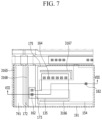
- FIG. 7 illustrates a layout view of a light emitting diode display device according to an exemplary embodiment
- FIG. 8 illustrates a cross-sectional view taken along line III-III of FIG. 1 .
- a light emitting diode display device includes the substrate 110 , the semiconductor 135 positioned on the substrate 110 , the gate electrode 154 positioned on the semiconductor 135 , the interlayer insulating layer 160 positioned on the substrate 110 and the gate electrode 154 , and the source electrode 173 and the drain electrode 175 positioned on the interlayer insulating layer 160 .
- Slits 3165 , 3166 , 3167 , and 3168 are provided in the interlayer insulating layer 160 , and the slits 3165 , 3166 , 3167 , and 3168 do not contact the semiconductor 135 and the gate electrode 154 .
- the slits 3165 , 3166 , 3167 , and 3168 expose the substrate 110 .
- the slit 3165 overlaps the common voltage line 741 .
- the common voltage line 741 contacts the substrate 110 through the slit 3165 .
- the slits 3166 and 3167 overlap the drain electrode 175 .
- the drain electrode 175 contacts the substrate 110 through the slits 3166 and 3167 .
- the slit 3168 overlaps the driving voltage line 172 and the source electrode 173 .
- the driving voltage line 172 and the source electrode 173 contact the substrate 110 through the slit 3168 .
- the slit 3168 may have a bar shape in a plan view, and may extend in a direction substantially parallel to the driving voltage line 172 .
- the slit 3168 may substantially extend in a vertical direction.
- the slit 3168 is positioned at the left side of the semiconductor 135 in a plan view, and it may be positioned to be adjacent to the left edge of the semiconductor 135 .
- the driving voltage line 172 is positioned in the slit 3168 , and the driving voltage line 172 may be made of an opaque metal material. Accordingly, light otherwise would be incident on the left surface of the semiconductor 135 may be blocked by the driving voltage line 172 positioned in the slit 3168 .
- the light incident on the lateral surface of the semiconductor 135 may be blocked by the common voltage line 741 , the drain electrode 175 , and the driving voltage line 172 positioned in the slits 3165 , 3166 , 3167 , and 3168 and made of an opaque metal material.
- the upper surface of the semiconductor 135 is mostly covered by the source electrode 173 and the drain electrode 175 , and thus light otherwise would be incident on the upper surface of the semiconductor 135 may also be blocked.
- the light incident on the upper and lateral surfaces of the semiconductor 135 may be blocked by using the common voltage line 741 , the drain electrode 175 , the driving voltage line 172 , the source electrode 173 , etc.
- the different metal layers are not positioned below the slits 3165 , 3166 , 3167 , and 3168 .
- the light emitting diode display device includes many portions that are the same as those in the light emitting diode display device according to the exemplary embodiment shown in FIG. 7 and FIG. 8 , which will not be described.
- a configuration in which the common voltage line, the drain electrode, the driving voltage line, and the source electrode do not contact the substrate is different from that of the previous exemplary embodiments, and will now be described in detail.
- FIG. 9 illustrates a cross-sectional view of a light emitting diode display device according to an exemplary embodiment.
- a light emitting diode display device includes the substrate 110 , the semiconductor 135 positioned on the substrate 110 , the gate electrode 154 positioned on the semiconductor 135 , the interlayer insulating layer 160 positioned on the substrate 110 and the gate electrode 154 , and the source electrode 173 and the drain electrode 175 positioned on the interlayer insulating layer 160 .
- Slits 4165 and 4168 are provided in the interlayer insulating layer 160 , and the slits 4165 and 4168 do not overlap the semiconductor 135 and the gate electrode 154 .
- the buffer layer 120 is further positioned between the substrate 110 and the semiconductor 135 , and the slits 4165 and 4168 expose the buffer layer 120 .
- the slit is provided in the buffer layer in the previous exemplary embodiment, the slit is not provided in the buffer layer in the present exemplary embodiment.
- the slit 4165 overlaps the common voltage line 741 .
- the common voltage line 741 may contact the buffer layer 120 through the slit 4165 , while it may not contact the substrate 110 .
- the slit 4168 overlaps the driving voltage line 172 and the source electrode 173 .
- the driving voltage line 172 and the source electrode 173 may contact the buffer layer 120 through the slit 4168 , while it may not contact the substrate 110 .
- the drain electrode 175 may also contact the buffer layer 120 through the slit, while it may not contact the substrate 110 .
- the light emitting diode display device includes many portions that are the same as those in the light emitting diode display device according to the exemplary embodiment shown in FIG. 1 to FIG. 3 , which will not be described.
- a configuration in which the gate electrode contacts the substrate is different from that of the previous exemplary embodiments, and will now be described in detail.
- FIG. 10 illustrates a layout view of a light emitting diode display device according to an exemplary embodiment
- FIG. 11 illustrates a cross-sectional view taken along line XI-XI of FIG. 10 .
- a light emitting diode display device includes the substrate 110 , the semiconductor 135 positioned on the substrate 110 , the gate insulating layer 140 positioned on the semiconductor 135 , the gate electrode 154 positioned on the gate insulating layer 140 , the interlayer insulating layer 160 positioned on the substrate 110 and the gate electrode 154 , and the source electrode 173 and the drain electrode 175 positioned on the interlayer insulating layer 160 .
- Slits 5166 and 5167 are provided in the buffer layer 120 and the interlayer insulating layer 160 , and a slit 5168 is provided in the buffer layer 120 and gate insulating layer 140 .
- the slits 5166 , 5167 , and 5168 do not overlap the semiconductor 135 .
- the slits 5166 , 5167 , and 5168 expose the substrate 110 .
- the slits 5166 and 5167 overlap the drain electrode 175 , while they do not overlap the gate electrode 154 .
- the drain electrode 175 contacts the substrate 110 through the slits 5166 and 5167 .
- the slit 5168 overlaps the gate electrode 154 .
- the gate electrode 154 contacts the substrate 110 through the slit 5168 .
- the slit 5168 may have a bar shape in a plan view, and may extend in a direction substantially parallel to the driving voltage line 172 .
- the slit 5168 may substantially extend in a vertical direction.
- the slit 5168 is positioned at the right side of the semiconductor 135 in a plan view, and may be positioned to be adjacent to the right edges of the semiconductor 135 .
- the gate electrode 154 is positioned in the slit 5168 , and the gate electrode 154 may be made of an opaque metal material. Accordingly, light otherwise would be incident on a right surface of the semiconductor 135 may be blocked by the gate electrode 154 positioned in the slit 5168 .
- the light incident on the lateral surface of the semiconductor 135 may be blocked by the drain electrode 175 and the gate electrode 154 positioned in the slits 5166 , 5167 , and 5168 and made of an opaque metal material.
- an upper surface of the semiconductor 135 is mostly covered by the source electrode 173 and the drain electrode 175 , and thus light otherwise would be incident on the upper surface of the semiconductor 135 may also be blocked.
- the light incident on the upper and lateral surfaces of the semiconductor 135 may be blocked by using the drain electrode 175 , the gate electrode 154 , the source electrode 173 , etc.
- the different metal layers are not positioned below the slits 5166 , 5167 , and 5168 .
- the light emitting diode display device includes many portions that are the same as those in the light emitting diode display device according to the exemplary embodiment shown in FIG. 10 and FIG. 11 , which will not be described.
- a configuration in which the drain electrode and the gate electrode do not contact the substrate is different from that of the previous exemplary embodiments, and will now be described in detail.
- FIG. 12 illustrates a cross-sectional view of a light emitting diode display device according to an exemplary embodiment.
- a light emitting diode display device includes the substrate 110 , the semiconductor 135 positioned on the substrate 110 , the gate insulating layer 140 positioned on the semiconductor 135 , the gate electrode 154 positioned on the gate insulating layer 140 , the interlayer insulating layer 160 positioned on the substrate 110 and the gate electrode 154 , and the source electrode 173 and the drain electrode 175 positioned on the interlayer insulating layer 160 .
- a slit 6168 is provided in the gate insulating layer 140 , and the slit 6168 does not overlap the semiconductor 135 .
- the buffer layer 120 is further positioned between the substrate 110 and the semiconductor 135 , and the slit 6168 exposes the buffer layer 120 .
- the slit is provided in the buffer layer in the previous exemplary embodiment, the slit is not provided in the buffer layer in the present exemplary embodiment.
- the slit 6168 overlaps the gate electrode 154 .
- the gate electrode 154 contacts the buffer layer 120 through the slit 6168 , while it may not contact the substrate 110 .
- the drain electrode 175 may also contact the buffer layer 120 through the slit, while it may not contact the substrate 110 .
- the light emitting diode display device includes many portions that are the same as those in the light emitting diode display device according to the exemplary embodiment shown in FIG. 10 and FIG. 11 , which will not be described.
- a configuration in which the common voltage line contacts the substrate is different from that of the previous exemplary embodiments, and will now be described in detail.
- FIG. 13 illustrates a layout view of a light emitting diode display device according to an exemplary embodiment
- FIG. 14 illustrates a cross-sectional view taken along line XIV-XIV of FIG. 13 .
- a light emitting diode display device includes the substrate 110 , the semiconductor 135 positioned on the substrate 110 , the gate insulating layer 140 positioned on the semiconductor 135 , the gate electrode 154 positioned on the gate insulating layer 140 , the interlayer insulating layer 160 positioned on the substrate 110 and the gate electrode 154 , and the source electrode 173 and the drain electrode 175 positioned on the interlayer insulating layer 160 .
- Slits 7165 , 7166 , and 7167 are provided in the buffer layer 120 and the interlayer insulating layer 160 , while a slit 7168 is provided in the buffer layer 120 and gate insulating layer 140 .
- the slits 7165 , 7166 , 7167 , and 7168 do not overlap the semiconductor 135 .
- the slits 7165 , 7166 , 7167 , and 7168 expose the substrate 110 .
- the slit 7165 overlaps the common voltage line 741 .
- the common voltage line 741 contacts the substrate 110 through the slit 7165 .
- the slits 7166 and 7167 overlap the drain electrode 175 .
- the drain electrode 175 contacts the substrate 110 through the slits 7166 and 7167 .
- the slit 7168 overlaps the gate electrode 154 .
- the gate electrode 154 contacts the substrate 110 through the slit 7168 .
- the light incident on the lateral surface of the semiconductor 135 may be blocked by the common voltage line 741 , the drain electrode 175 , and the gate electrode 154 positioned in the slits 7165 , 7166 , 7167 , and 7168 and made of an opaque metal material.
- the upper surface of the semiconductor 135 is mostly covered by the source electrode 173 and the drain electrode 175 , and thus light incident otherwise would be on the upper surface of the semiconductor 135 may also be blocked.
- the light incident on the upper and lateral surfaces of the semiconductor 135 may be blocked by using the common voltage line 741 , the drain electrode 175 , the gate electrode 154 , and the source electrode 173 , etc.
- the different metal layers are not positioned below the slits 7165 , 7166 , 7167 , and 7168 .
- the light emitting diode display device includes many portions that are the same as those in the light emitting diode display device according to the exemplary embodiment shown in FIG. 13 and FIG. 14 , which will not be described.
- a configuration in which the common voltage line, the drain electrode, and the gate electrode do not contact the substrate is different from that of the previous exemplary embodiments, and will now be described in detail.
- FIG. 15 illustrates a cross-sectional view of a light emitting diode display device according to an exemplary embodiment.
- a light emitting diode display device includes the substrate 110 , the semiconductor 135 positioned on the substrate 110 , the gate insulating layer 140 positioned on the semiconductor 135 , the gate electrode 154 positioned on the gate insulating layer 140 , the interlayer insulating layer 160 positioned on the substrate 110 and the gate electrode 154 , and the source electrode 173 and the drain electrode 175 positioned on the interlayer insulating layer 160 .
- a slit 8165 is provided in the interlayer insulating layer 160 , and a slit 8168 is provided in the gate insulating layer 140 .
- the slits 8165 and 8168 do not overlap the semiconductor 135 .
- the buffer layer 120 is further positioned between the substrate 110 and the semiconductor 135 , and the slits 8165 and 8168 expose the buffer layer 120 .
- the slit is provided in the buffer layer in the previous exemplary embodiment, the slit is not provided in the buffer layer in the present exemplary embodiment.
- the slit 8165 overlaps the common voltage line 741 .
- the common voltage line 741 contacts the buffer layer 120 through the slit 8165 , while it may not contact the substrate 110 .
- the slit 8168 overlaps the gate electrode 154 .
- the gate electrode 154 contacts the buffer layer 120 through the slit 8168 , while it may not contact the substrate 110 .
- the drain electrode 175 may also contact the buffer layer 120 through the slit, while it may not contact the substrate 110 .
- FIG. 16 illustrates a layout view of a light emitting diode display device according to an exemplary embodiment.
- a light emitting diode display device includes a substrate (not shown), and a first thin film transistor (Ta), a second thin film transistor (Tb), a third thin film transistor (Tc), and a first electrode 191 that are positioned on the substrate.
- the light emitting diode display device may further include the common voltage line 741 , the driving voltage line 172 , a data line 171 , and a sensing line 176 .
- the first thin film transistor (Ta) includes a first gate electrode 1154 a , a first semiconductor 1135 a , a first source electrode 1173 a , and a first drain electrode 1175 a .
- the first source electrode 1173 a is connected to the driving voltage line 172 .
- the first semiconductor 1135 a overlaps the first gate electrode 1154 a .
- Some region of the first semiconductor 1135 a is connected to the first source electrode 1173 a
- some other region of the first semiconductor 1135 a is connected to the first drain electrode 1175 a .
- the first thin film transistor (Ta) may be a driving thin film transistor.
- the second thin film transistor (Tb) includes a second gate electrode 1154 b , a second semiconductor 1135 b , a second source electrode 1173 b , and a second drain electrode 1175 b .
- the second source electrode 1173 b is connected to the data line 171 .
- the second semiconductor 1135 b overlaps the second gate electrode 1154 b .
- Some region of the second semiconductor 1135 b is connected to the second source electrode 1173 b
- some other region of the second semiconductor 1135 b is connected to the second drain electrode 1175 b .
- the second drain electrode 1175 b is connected to the first gate electrode 1154 a .
- the second thin film transistor (Tb) may be a switching thin film transistor.
- the third thin film transistor (Tc) includes a third gate electrode 1154 c , a third semiconductor 1135 c , a third source electrode 1173 c , and a third drain electrode 1175 c .
- the third source electrode 1173 c is connected to the sensing line 176 .
- the third semiconductor 1135 c overlaps the third gate electrode 1154 c .
- Some region of the third semiconductor 1135 c is connected to the third source electrode 1173 c
- some other region of the third semiconductor 1135 c is connected to the third drain electrode 1175 c .
- the third drain electrode 1175 c is connected to the first drain electrode 1175 a .
- the third thin film transistor (Tc) may be a sensing switching thin film transistor.
- the first electrode 191 is formed to have a substantially quadrangular shape, and overlaps the first thin film transistor (Ta), the second thin film transistor (Tb), and the third thin film transistor (Tc). Particularly, the first electrode 191 overlaps most regions of the first semiconductor 1135 a , the second semiconductor 1135 b , and the third semiconductor 1135 c .
- the first electrode 191 may include a reflective metal material. Accordingly, since the first electrode 191 covers most regions of the first semiconductor 1135 a , the second semiconductor 1135 b , and the third semiconductor 1135 c , light incident on upper surfaces of the first semiconductor 1135 a , the second semiconductor 1135 b , and the third semiconductor 1135 c may be blocked.
- the light emitting diode display device includes many portions that are the same as those in the light emitting diode display device according to the exemplary embodiment shown in FIG. 16 , which will not be described.
- a configuration in which slits overlapping the common voltage line, the driving voltage line, and the first gate electrode are further formed is different from that of the previous exemplary embodiments, and will now be described in detail.
- FIG. 17 illustrates a layout view of a light emitting diode display device according to an exemplary embodiment.
- a light emitting diode display device includes a substrate (not shown), and a first thin film transistor (Ta), a second thin film transistor (Tb), a third thin film transistor (Tc), and a first electrode 191 that are positioned on the substrate.
- the light emitting diode display device may further include the common voltage line 741 , the driving voltage line 172 , the data line 171 , and the sensing line 176 .
- the interlayer insulating layer (not shown) may be positioned between the substrate and the common voltage line 741 and between the substrate and the driving voltage line 172 .
- Slits 9165 and 9168 are provided in the interlayer insulating layer.
- the gate insulating layer (not shown) may be positioned between the substrate and the first gate electrode 1154 a .
- a slit 9167 is provided in the gate insulating layer.
- the slit 9165 overlaps the common voltage line 741 .
- the common voltage line 741 contacts the substrate through the slit 9165 .
- the slit 9168 overlaps the driving voltage line 172 .
- the driving voltage line 172 contacts the substrate through the slit 9168 .
- the slit 9167 overlaps the first gate electrode 1154 a .
- the first gate electrode 1154 a contacts the substrate through the slit 9167 .
- the buffer layer may be further positioned below the interlayer insulating layer and the gate insulating layer.
- the slits 9165 , 9167 , and 9168 may be provided in the buffer layer.
- the slits 9165 , 9167 , and 9168 may not be provided in the buffer layer, while they may be provided only in the interlayer insulating layer and the gate insulating layer.
- the common voltage line 741 , the driving voltage line 172 , and the first gate electrode 1154 a do not contact the substrate, while they contact the buffer layer.
- FIG. 18 illustrates a schematic view of a light emitting diode display device according to an exemplary embodiment
- FIG. 19 illustrates a layout view of a thin film transistor included in a gate driver of a light emitting diode display device according to an exemplary embodiment
- FIG. 20 illustrates a cross-sectional view taken along line XX-XX of FIG. 19
- FIG. 21 illustrates a cross-sectional view taken along line XXI-XXI of FIG. 19 .
- a light emitting diode display device includes a display panel 300 , a data driver 460 , a gate driver 500 , a signal controller 600 , etc.
- the display panel 300 includes a display area (DA) displaying an image, and a peripheral area (PA) surrounding the display area (DA).
- the gate driver 500 for applying gate voltages to gate lines (G 1 to Gn) is disposed in the peripheral area (PA).
- Data lines (D 1 to Dm) of the display area (DA) may receive data voltages from the data driver 460 .
- the data driver 460 may be an integrated circuit (IC) disposed on a flexible printed circuit board (FPCB) 450 attached to the display panel 300 .
- the gate driver 500 and the data driver 460 are controlled by the signal controller 600 .
- a printed circuit board (PCB) 400 is positioned at the outside of the flexible printed circuit board 450 and configured to transmit a signal from the signal controller 600 to the data driver 460 and the gate driver 500 .
- the signal transmitted to the gate driver 500 from the signal controller 600 through a plurality of signal lines SL may include a signal such as a vertical start signal, a clock signal, and a low voltage signal of a predetermined level.
- a plurality of pixels PX may be disposed in the display area (DA), and the plurality of gate lines (G 1 to Gn) and the plurality of data lines (D 1 to Dm) may cross while being insulated from each other.
- the data lines (D 1 to Dm) receive the data voltages from the data driver 460
- the gate lines (G 1 to Gn) receive gate voltages from the gate driver 500 .
- the data driver 460 may be positioned on an upper or lower side of the display panel 300 and connected to the data lines (D 1 to Dm) extending in a vertical direction.
- the gate driver 500 receives a vertical start signal, a clock signal, and a low voltage corresponding to a gate-off voltage, and generates gate voltages (a gate-on voltage and a gate-off voltage) and applies them to the gate lines (G 1 to Gn).
- the gate driver 500 may include a plurality of stages for generating and outputting gate voltages through the signals, and each stage may include a plurality of thin film transistors.
- the gate driver 500 may be integrated in the peripheral area (PA) of the display panel 300 .
- a gate driver of a light emitting diode display device may include the thin film transistor (TR) and a capacitor (CAP).
- a plurality of thin film transistors (TR) may be disposed in one gate driver.
- the plurality of thin film transistors (TR) may be disposed in a matrix form.
- the capacitor (CAP) may be disposed at end portions of the plurality of thin film transistors (TR).
- the capacitor (CAP) is disposed at right end portions of the plurality of thin film transistors (TR).
- the display area (DA) of the display panel 300 may be disposed at a right side of the capacitor (CAP). That is, the capacitor (CAP) may be disposed between the plurality of thin film transistors (TR) and the display area (DA).
- a position of the capacitor (CAP) is not limited thereto, and the capacitor (CAP) may be disposed at left end portions of the plurality of thin film transistors (TR).
- the plurality of thin film transistors (TR) may be disposed between the capacitor (CAP) and the display area (DA).
- the thin film transistor (TR) includes a lower gate electrode 2124 , a semiconductor 2135 , an upper gate electrode 2154 , a source electrode 2173 , and a drain electrode 2175 .
- the lower gate electrode 2124 is positioned on the substrate 110 .
- the lower gate electrode 2124 may overlap some of the semiconductor 2135 .
- the lower gate electrode 2124 may block light that passes through the substrate 110 from being incident on the semiconductor 2135 .
- a first insulating layer 140 a may be positioned the lower gate electrode 2124 .
- the first insulating layer 140 a may include an inorganic insulating material or organic insulating material such as a silicon oxide (SiOx), a silicon nitride (SiNx), silicon oxynitride (SiON), silicon oxyfluoride (SiOF), an aluminum oxide (AlOx), etc., and it may be formed as a single layer or a multilayer including at least one of the materials.
- the semiconductor 2135 is positioned on the first insulating layer 140 a .
- the semiconductor 2135 may overlap some of the lower gate electrode 2124 in a direction perpendicular to the substrate 110 .
- the semiconductor 2135 may be made of an oxide semiconductor material.
- the semiconductor 2135 may be an indium-gallium-zinc oxide (IGZO) or an indium-tin-zinc oxide (ITZO).
- a second insulating layer 140 b may be positioned the semiconductor 2135 .
- the second insulating layer 140 b may include an inorganic insulating material or organic insulating material such as a silicon oxide (SiOx), a silicon nitride (SiNx), silicon oxynitride (SiON), silicon oxyfluoride (SiOF), an aluminum oxide (AlOx), etc., and it may be formed as a single layer or a multilayer including at least one of the materials.
- the upper gate electrode 2154 is positioned on the second insulating layer 140 b .
- the upper gate electrode 2154 overlaps the semiconductor 2135 with the second insulating layer 140 b therebetween.
- the upper gate electrode 2154 may be electrically connected to the lower gate electrode 2124 .
- a slit 10163 may be provided in the first insulating layer 140 a .
- the upper gate electrode 2154 may be connected to the lower gate electrode 2124 through the slit 10163 to have a dual gate structure.
- the interlayer insulating layer 160 is positioned on the upper gate electrode 2154 .
- the interlayer insulating layer 160 may include an inorganic insulating material or organic insulating material such as a silicon oxide (SiOx), a silicon nitride (SiNx), silicon oxynitride (SiON), silicon oxyfluoride (SiOF), an aluminum oxide (AlOx), etc., and it may be formed as a single layer or a multilayer including at least one of the materials.
- the source electrode 2173 and the drain electrode 2175 are positioned on the interlayer insulating layer 160 .
- the source electrode 2173 may include a first portion that extends in a substantially horizontal direction, and a second portion that protrudes from the first portion and extends in a substantially vertical direction to overlap the semiconductor 2135 .
- the drain electrode 2175 may include a first portion that extends in a substantially horizontal direction, and a second portion that protrudes from the first portion and extends in a substantially vertical direction to overlap the semiconductor 2135 .
- the source electrode 2173 protrudes toward the drain electrode 2175
- the drain electrode 2175 protrudes toward the source electrode 2173 .
- Slits 10162 and 10164 are provided in the interlayer insulating layer 160 .
- the slit 10162 overlaps the source electrode 2173 and the semiconductor 2135 .
- the source electrode 2173 is connected to the semiconductor 2135 through the slit 10162 .
- the slit 10164 overlaps the drain electrode 2175 and the semiconductor 2135 .
- the drain electrode 2175 is connected to the semiconductor 2135 through the slit 10164 .
- Slits 10165 and 10166 are further provided in the first insulating layer 140 a and the interlayer insulating layer 160 .
- the slits 10165 and 10166 do not overlap the semiconductor 2135 , the lower gate electrode 2124 , and the upper gate electrode 2154 .
- the slits 10165 and 10166 expose the substrate 110 .
- the slit 10165 overlaps the source electrode 2173 .
- the source electrode 2173 contacts the substrate 110 through the slit 10165 .
- the slit 10165 may have a bar shape in a plan view, and may extend in a direction substantially parallel to the source electrode 2173 .
- the slit 10165 may substantially extend in a horizontal direction.
- the slit 10165 is positioned at an upper side of an uppermost semiconductor 2135 in a plan view, and may be positioned to be adjacent to an upper edge of the uppermost semiconductor 2135 .
- the source electrode 2173 is positioned in the slit 10165 , and the source electrode 2173 may be made of an opaque metal material. Accordingly, light otherwise would be incident on an upper surface of the semiconductor 2135 may be blocked by the source electrode 2173 positioned in the slit 10165 .
- the slit 10166 overlaps the drain electrode 2175 .
- the drain electrode 2175 contacts the substrate 110 through the slit 10166 .
- the slit 10166 may have a bar shape in a plan view, and may extend in a direction substantially parallel to the drain electrode 2175 .
- the slit 10166 may substantially extend in a horizontal direction.
- the slit 10166 is positioned at a lower side of a lowermost semiconductor 2135 in a plan view, and may be positioned to be adjacent to a lower edge of the lower side of a lowermost semiconductor 2135 .
- the drain electrode 2175 is positioned in the slit 10166 , and the drain electrode 2175 may be made of an opaque metal material. Accordingly, light otherwise would be incident on a lower surface of the semiconductor 2135 may be blocked by the drain electrode 2175 positioned in the slit 10166 .
- the capacitor (CAP) includes a first capacitor electrode 210 , the interlayer insulating layer 160 , and a second capacitor electrode 230 .
- the first capacitor electrode 210 is positioned on the first insulating layer 140 a , and is electrically connected to the upper gate electrode 2154 .
- the first capacitor electrode 210 may be positioned at the same layer as the upper gate electrode 2154 , and may be made of the same material as that the upper gate electrode 2154 .
- the second capacitor electrode 230 is positioned to overlap the first capacitor electrode 210 .
- the interlayer insulating layer 160 is positioned between the first capacitor electrode 210 and the second capacitor electrode 230 .
- the interlayer insulating layer 160 may serve as a dielectric material.
- the second capacitor electrode 230 is electrically connected to the drain electrode 2175 .
- the second capacitor electrode 230 may be positioned at the same layer as the source electrode 2173 and the drain electrode 2175 , and may be made of the same material as that of the source electrode 2173 and the drain electrode 2175 .
- a slit 10167 is further provided in the first insulating layer 140 a .
- the slit 10167 does not overlap the semiconductor 2135 .
- the slit 10167 exposes the substrate 110 .
- the slit 10167 overlaps the first capacitor electrode 210 .
- the first capacitor electrode 210 contacts the substrate 110 through the slit 10167 .
- the slit 10167 may have a bar shape in a plan view, and may substantially extend in a vertical direction.
- the slit 10167 is positioned at right sides of semiconductors 2135 in a plan view, and may be positioned to be adjacent to right edges of the semiconductors 2135 .
- the first capacitor electrode 210 is positioned in the slit 10167 , and the first capacitor electrode 210 may be made of an opaque metal material. Accordingly, light otherwise would be incident on a lateral surface of the semiconductor 2135 may be blocked by the first capacitor electrode 210 positioned in the slit 10167 .
- the source electrode 2173 , the drain electrode 2175 , and the first capacitor electrode 210 that are positioned in the slits 10165 , 10166 , and 10167 and made of an opaque metal material.
- the upper surface of the semiconductor 2135 is mostly covered by the source electrode 2173 , the drain electrode 2175 , and the upper gate electrode 2154 , light otherwise would be incident on the upper surface of the semiconductor 2135 may also be blocked.
- light otherwise would be incident on the upper and lateral surfaces of the semiconductor 2135 may be blocked by using the source electrode 2173 , the drain electrode 2175 , the first capacitor electrode 210 , etc.
- the different metal layers are not positioned below the slits 10165 , 10166 , and 10167 .
- the buffer layer may be further positioned below the interlayer insulating layer 160 and the first insulating layer 140 a .
- the slits 10165 , 10166 , and 10167 may be provided in the buffer layer.
- the slits 10165 , 10166 , and 10167 may not be provided in the buffer layer, while they may be provided only in the interlayer insulating layer 160 and the first insulating layer 140 a .
- the source electrode 2173 , the drain electrode 2175 , and the first capacitor electrode 210 do not contact the substrate 110 , while they contact the buffer layer.
Abstract
Description
Claims (22)
Priority Applications (1)
| Application Number | Priority Date | Filing Date | Title |
|---|---|---|---|
| US16/882,260 US11574975B2 (en) | 2016-09-20 | 2020-05-22 | Light emitting diode display device with channel region covered by drain electrode |
Applications Claiming Priority (4)
| Application Number | Priority Date | Filing Date | Title |
|---|---|---|---|
| KR1020160120119A KR102573853B1 (en) | 2016-09-20 | 2016-09-20 | Light emitting diode display device |
| KR10-2016-0120119 | 2016-09-20 | ||
| US15/707,637 US10665655B2 (en) | 2016-09-20 | 2017-09-18 | Light emitting diode display device |
| US16/882,260 US11574975B2 (en) | 2016-09-20 | 2020-05-22 | Light emitting diode display device with channel region covered by drain electrode |
Related Parent Applications (1)
| Application Number | Title | Priority Date | Filing Date |
|---|---|---|---|
| US15/707,637 Continuation US10665655B2 (en) | 2016-09-20 | 2017-09-18 | Light emitting diode display device |
Publications (2)
| Publication Number | Publication Date |
|---|---|
| US20200286973A1 US20200286973A1 (en) | 2020-09-10 |
| US11574975B2 true US11574975B2 (en) | 2023-02-07 |
Family
ID=59955368
Family Applications (2)
| Application Number | Title | Priority Date | Filing Date |
|---|---|---|---|
| US15/707,637 Active US10665655B2 (en) | 2016-09-20 | 2017-09-18 | Light emitting diode display device |
| US16/882,260 Active US11574975B2 (en) | 2016-09-20 | 2020-05-22 | Light emitting diode display device with channel region covered by drain electrode |
Family Applications Before (1)
| Application Number | Title | Priority Date | Filing Date |
|---|---|---|---|
| US15/707,637 Active US10665655B2 (en) | 2016-09-20 | 2017-09-18 | Light emitting diode display device |
Country Status (4)
| Country | Link |
|---|---|
| US (2) | US10665655B2 (en) |
| EP (1) | EP3297028B1 (en) |
| KR (1) | KR102573853B1 (en) |
| CN (1) | CN107845660B (en) |
Families Citing this family (4)
| Publication number | Priority date | Publication date | Assignee | Title |
|---|---|---|---|---|
| KR102642017B1 (en) * | 2016-11-30 | 2024-02-28 | 엘지디스플레이 주식회사 | Organic light emitting display device |
| US10971527B2 (en) * | 2018-09-11 | 2021-04-06 | Sharp Kabushiki Kaisha | Thin-film transistor substrate including data line with lower layer data line and upper layer data line, and liquid crystal display device and organic electroluminescent display device including same |
| CN109616497A (en) * | 2018-11-30 | 2019-04-12 | 武汉华星光电技术有限公司 | OLED display panel |
| US11289673B2 (en) * | 2019-08-06 | 2022-03-29 | Wuhan China Star Optoelectronics Semiconductor Display Technology Co., Ltd. | Display panel having Bragg mirror and manufacturing method of same |
Citations (29)
| Publication number | Priority date | Publication date | Assignee | Title |
|---|---|---|---|---|
| US20020101152A1 (en) | 2001-01-30 | 2002-08-01 | Semiconductor Energy Laboratory Co., Ltd. | Light emitting device |
| US20020104995A1 (en) | 2001-01-17 | 2002-08-08 | Shunpei Yamazaki | Light emitting device |
| JP2003084687A (en) | 2001-05-23 | 2003-03-19 | Semiconductor Energy Lab Co Ltd | Semiconductor device and method of fabricating the same |
| US20030116768A1 (en) | 2001-05-23 | 2003-06-26 | Semiconductor Energy Laboratory Co., Ltd. | Semiconductor device and manufacturing method thereof |
| US20050168135A1 (en) | 2003-12-16 | 2005-08-04 | Nec Corporation | Luminescence display apparatus and method for fabricating the same |
| US20070216280A1 (en) * | 2006-03-14 | 2007-09-20 | Seiko Epson Corporation | Organic electroluminescent device and electronic apparatus |
| EP1863095A2 (en) | 2006-06-01 | 2007-12-05 | Samsung Electronics Co., Ltd. | Thin film transistor array panel and method of manufacturing the same |
| CN101179110A (en) | 2006-11-10 | 2008-05-14 | 三星Sdi株式会社 | Organic light emitting display and fabrication method thereof |
| US20100002173A1 (en) | 2008-07-04 | 2010-01-07 | Miharu Otani | Liquid Crystal Display Device and Manufacturing Method for Same |
| US20100065952A1 (en) | 2008-09-18 | 2010-03-18 | Semiconductor Energy Laboratory Co., Ltd. | Semiconductor Device |
| US20110108841A1 (en) | 2008-06-27 | 2011-05-12 | Junichi Hanna | Semiconductor device, manufacturing method thereof, and display apparatus using the semiconductor device |
| US20110108844A1 (en) * | 2005-05-12 | 2011-05-12 | Samsung Mobile Display Co., Ltd. | Organic light emitting display |
| US8207531B2 (en) | 2009-08-25 | 2012-06-26 | Canon Kabushiki Kaisha | Thin film transistor, display device using thin film transistor, and production method of thin film transistor |
| US20120168756A1 (en) | 2010-12-31 | 2012-07-05 | Inha-Industry Partnership Institute | Transistor, Method Of Manufacturing The Same, And Electronic Device Including The Transistor |
| US8304710B2 (en) | 2006-01-10 | 2012-11-06 | Semiconductor Energy Laboratory Co., Ltd. | Display device and manufacturing method thereof |
| US8304981B2 (en) | 2008-12-01 | 2012-11-06 | Samsung Display Co., Ltd. | Organic light emitting diode display and manufacturing method thereof |
| US20120305921A1 (en) * | 2011-06-03 | 2012-12-06 | Byoung-Keon Park | Thin film transistor, manufacturing method of thin film transistor, and organic light emitting diode display including the same |
| US8502230B2 (en) | 2010-06-04 | 2013-08-06 | Samsung Display Co., Ltd. | Organic light-emitting display |
| US20130256652A1 (en) * | 2012-04-02 | 2013-10-03 | Yong Su LEE | Thin film transistor, thin film transistor array panel including the same, and method of manufacturing the same |
| US8587006B2 (en) | 2009-11-26 | 2013-11-19 | Samsung Display Co., Ltd. | Organic light-emitting display |
| US20140203285A1 (en) | 2013-01-18 | 2014-07-24 | Seiko Epson Corporation | Electrooptic device substrate, electrooptic device, and electronic apparatus |
| CN104217675A (en) | 2013-05-30 | 2014-12-17 | 三星显示有限公司 | Organic light emitting diode display and pixel circuit of display device |
| US20150021564A1 (en) * | 2013-07-22 | 2015-01-22 | Samsung Display Co., Ltd. | Organic light emitting diode display |
| US20150155169A1 (en) | 2013-11-29 | 2015-06-04 | Semiconductor Energy Laboratory Co., Ltd. | Manufacturing method of semiconductor device |
| US20150357356A1 (en) * | 2014-06-10 | 2015-12-10 | Samsung Display Co., Ltd. | Thin film transistor array substrate and method of manufacturing the same |
| US20160063924A1 (en) | 2014-08-29 | 2016-03-03 | Lg Display Co., Ltd. | Thin film transistor substrate and display using the same |
| US20160372662A1 (en) | 2014-03-03 | 2016-12-22 | Fujifilm Corporation | Organic thin-film transistor and method for manufacturing same |
| US20170012093A1 (en) * | 2014-01-29 | 2017-01-12 | Joled Inc. | Image display apparatus |
| US20180061927A1 (en) * | 2016-08-31 | 2018-03-01 | Lg Display Co., Ltd. | Thin film transistor substrate for flat panel display |
-
2016
- 2016-09-20 KR KR1020160120119A patent/KR102573853B1/en active IP Right Grant
-
2017
- 2017-09-18 US US15/707,637 patent/US10665655B2/en active Active
- 2017-09-19 EP EP17191903.8A patent/EP3297028B1/en active Active
- 2017-09-20 CN CN201710851843.6A patent/CN107845660B/en active Active
-
2020
- 2020-05-22 US US16/882,260 patent/US11574975B2/en active Active
Patent Citations (34)
| Publication number | Priority date | Publication date | Assignee | Title |
|---|---|---|---|---|
| US20020104995A1 (en) | 2001-01-17 | 2002-08-08 | Shunpei Yamazaki | Light emitting device |
| US20020101152A1 (en) | 2001-01-30 | 2002-08-01 | Semiconductor Energy Laboratory Co., Ltd. | Light emitting device |
| JP2003084687A (en) | 2001-05-23 | 2003-03-19 | Semiconductor Energy Lab Co Ltd | Semiconductor device and method of fabricating the same |
| US20030116768A1 (en) | 2001-05-23 | 2003-06-26 | Semiconductor Energy Laboratory Co., Ltd. | Semiconductor device and manufacturing method thereof |
| US20050168135A1 (en) | 2003-12-16 | 2005-08-04 | Nec Corporation | Luminescence display apparatus and method for fabricating the same |
| US20110108844A1 (en) * | 2005-05-12 | 2011-05-12 | Samsung Mobile Display Co., Ltd. | Organic light emitting display |
| US8304710B2 (en) | 2006-01-10 | 2012-11-06 | Semiconductor Energy Laboratory Co., Ltd. | Display device and manufacturing method thereof |
| US20070216280A1 (en) * | 2006-03-14 | 2007-09-20 | Seiko Epson Corporation | Organic electroluminescent device and electronic apparatus |
| EP1863095A2 (en) | 2006-06-01 | 2007-12-05 | Samsung Electronics Co., Ltd. | Thin film transistor array panel and method of manufacturing the same |
| US20070278492A1 (en) | 2006-06-01 | 2007-12-06 | Samsung Electronics Co., Ltd. | Thin film transistor array panel and method of manufacturing the same |
| CN101179110A (en) | 2006-11-10 | 2008-05-14 | 三星Sdi株式会社 | Organic light emitting display and fabrication method thereof |
| US8536567B2 (en) | 2006-11-10 | 2013-09-17 | Samsung Display Co., Ltd. | Organic light emitting display and fabrication method thereof |
| US20110108841A1 (en) | 2008-06-27 | 2011-05-12 | Junichi Hanna | Semiconductor device, manufacturing method thereof, and display apparatus using the semiconductor device |
| US20100002173A1 (en) | 2008-07-04 | 2010-01-07 | Miharu Otani | Liquid Crystal Display Device and Manufacturing Method for Same |
| US20100065952A1 (en) | 2008-09-18 | 2010-03-18 | Semiconductor Energy Laboratory Co., Ltd. | Semiconductor Device |
| US8304981B2 (en) | 2008-12-01 | 2012-11-06 | Samsung Display Co., Ltd. | Organic light emitting diode display and manufacturing method thereof |
| US8207531B2 (en) | 2009-08-25 | 2012-06-26 | Canon Kabushiki Kaisha | Thin film transistor, display device using thin film transistor, and production method of thin film transistor |
| US8587006B2 (en) | 2009-11-26 | 2013-11-19 | Samsung Display Co., Ltd. | Organic light-emitting display |
| US8502230B2 (en) | 2010-06-04 | 2013-08-06 | Samsung Display Co., Ltd. | Organic light-emitting display |
| US20120168756A1 (en) | 2010-12-31 | 2012-07-05 | Inha-Industry Partnership Institute | Transistor, Method Of Manufacturing The Same, And Electronic Device Including The Transistor |
| US20120305921A1 (en) * | 2011-06-03 | 2012-12-06 | Byoung-Keon Park | Thin film transistor, manufacturing method of thin film transistor, and organic light emitting diode display including the same |
| US20130256652A1 (en) * | 2012-04-02 | 2013-10-03 | Yong Su LEE | Thin film transistor, thin film transistor array panel including the same, and method of manufacturing the same |
| US20140203285A1 (en) | 2013-01-18 | 2014-07-24 | Seiko Epson Corporation | Electrooptic device substrate, electrooptic device, and electronic apparatus |
| US9608050B2 (en) | 2013-05-30 | 2017-03-28 | Samsung Display Co., Ltd | Organic light emitting diode display utilizing a curved semiconductor layer |
| CN104217675A (en) | 2013-05-30 | 2014-12-17 | 三星显示有限公司 | Organic light emitting diode display and pixel circuit of display device |
| US10522604B2 (en) | 2013-05-30 | 2019-12-31 | Samsung Display Co., Ltd. | Organic light emitting diode display utilizing a curved semiconductor layer |
| US9117783B2 (en) | 2013-05-30 | 2015-08-25 | Samsung Display Co., Ltd. | Organic light emitting diode display including a gate insulating layer supporting a driving voltage line and a data line |
| US20150021564A1 (en) * | 2013-07-22 | 2015-01-22 | Samsung Display Co., Ltd. | Organic light emitting diode display |
| US20150155169A1 (en) | 2013-11-29 | 2015-06-04 | Semiconductor Energy Laboratory Co., Ltd. | Manufacturing method of semiconductor device |
| US20170012093A1 (en) * | 2014-01-29 | 2017-01-12 | Joled Inc. | Image display apparatus |
| US20160372662A1 (en) | 2014-03-03 | 2016-12-22 | Fujifilm Corporation | Organic thin-film transistor and method for manufacturing same |
| US20150357356A1 (en) * | 2014-06-10 | 2015-12-10 | Samsung Display Co., Ltd. | Thin film transistor array substrate and method of manufacturing the same |
| US20160063924A1 (en) | 2014-08-29 | 2016-03-03 | Lg Display Co., Ltd. | Thin film transistor substrate and display using the same |
| US20180061927A1 (en) * | 2016-08-31 | 2018-03-01 | Lg Display Co., Ltd. | Thin film transistor substrate for flat panel display |
Non-Patent Citations (1)
| Title |
|---|
| European Search Report corresponding to EP Application 17191903, dated Jan. 19, 2018, 8 pages. |
Also Published As
| Publication number | Publication date |
|---|---|
| KR102573853B1 (en) | 2023-09-01 |
| US10665655B2 (en) | 2020-05-26 |
| US20200286973A1 (en) | 2020-09-10 |
| KR20180031882A (en) | 2018-03-29 |
| US20180083085A1 (en) | 2018-03-22 |
| CN107845660B (en) | 2023-05-23 |
| EP3297028A1 (en) | 2018-03-21 |
| EP3297028B1 (en) | 2023-01-11 |
| CN107845660A (en) | 2018-03-27 |
Similar Documents
| Publication | Publication Date | Title |
|---|---|---|
| KR102158771B1 (en) | Organic light emitting diode display | |
| KR102391361B1 (en) | Organic light emitting diode display | |
| US11574975B2 (en) | Light emitting diode display device with channel region covered by drain electrode | |
| KR102101362B1 (en) | Organic light emitting diode diode display | |
| KR100989135B1 (en) | Organic light emitting diode display | |
| KR102090200B1 (en) | Organic light emitting diode display | |
| US9064833B2 (en) | Organic light emitting diode display | |
| KR102307432B1 (en) | Display device | |
| CN116705801A (en) | Display device | |
| US11107867B2 (en) | Display device and manufacturing method thereof | |
| US10854845B2 (en) | Display device | |
| US9741770B2 (en) | Organic light emitting diode display | |
| US9559330B2 (en) | Organic light emitting diode display | |
| KR20180025382A (en) | Organic light emitting display device | |
| US9911802B2 (en) | Display device and method for manufacturing the same | |
| KR102582466B1 (en) | Display device | |
| KR101975957B1 (en) | Organic light emitting diode display | |
| US20150042634A1 (en) | Organic light emitting diode display | |
| KR102247825B1 (en) | Bottom Emission Type Organic Light Emission Diode Display Having Color Filters And Method For Manufacturing The Same | |
| US10833142B2 (en) | Electroluminescence display device | |
| KR102269099B1 (en) | Thin film Transistor Substrate For Flat Panel Display And Method For Manufacturing The Same | |
| KR100989132B1 (en) | Organic light emitting diode display | |
| KR20160083641A (en) | Organic electro luminescent device |
Legal Events
| Date | Code | Title | Description |
|---|---|---|---|
| AS | Assignment |
Owner name: SAMSUNG DISPLAY CO., LTD., KOREA, REPUBLIC OF Free format text: ASSIGNMENT OF ASSIGNORS INTEREST;ASSIGNORS:MOON, SUNG-JAE;KIM, DONG GYU;PARK, SUN;REEL/FRAME:052739/0393 Effective date: 20170217 |
|
| FEPP | Fee payment procedure |
Free format text: ENTITY STATUS SET TO UNDISCOUNTED (ORIGINAL EVENT CODE: BIG.); ENTITY STATUS OF PATENT OWNER: LARGE ENTITY |
|
| STPP | Information on status: patent application and granting procedure in general |
Free format text: DOCKETED NEW CASE - READY FOR EXAMINATION |
|
| STPP | Information on status: patent application and granting procedure in general |
Free format text: NON FINAL ACTION MAILED |
|
| STPP | Information on status: patent application and granting procedure in general |
Free format text: RESPONSE TO NON-FINAL OFFICE ACTION ENTERED AND FORWARDED TO EXAMINER |
|
| STPP | Information on status: patent application and granting procedure in general |
Free format text: FINAL REJECTION MAILED |
|
| STPP | Information on status: patent application and granting procedure in general |
Free format text: RESPONSE AFTER FINAL ACTION FORWARDED TO EXAMINER |
|
| STPP | Information on status: patent application and granting procedure in general |
Free format text: ADVISORY ACTION MAILED |
|
| STPP | Information on status: patent application and granting procedure in general |
Free format text: DOCKETED NEW CASE - READY FOR EXAMINATION |
|
| STPP | Information on status: patent application and granting procedure in general |
Free format text: NON FINAL ACTION MAILED |
|
| STPP | Information on status: patent application and granting procedure in general |
Free format text: RESPONSE TO NON-FINAL OFFICE ACTION ENTERED AND FORWARDED TO EXAMINER |
|
| STPP | Information on status: patent application and granting procedure in general |
Free format text: NOTICE OF ALLOWANCE MAILED -- APPLICATION RECEIVED IN OFFICE OF PUBLICATIONS |
|
| STPP | Information on status: patent application and granting procedure in general |
Free format text: AWAITING TC RESP., ISSUE FEE NOT PAID |
|
| STPP | Information on status: patent application and granting procedure in general |
Free format text: NOTICE OF ALLOWANCE MAILED -- APPLICATION RECEIVED IN OFFICE OF PUBLICATIONS |
|
| STCF | Information on status: patent grant |
Free format text: PATENTED CASE |