US11572271B2 - Method for manufacturing an etch stop layer and MEMS sensor comprising an etch stop layer - Google Patents
Method for manufacturing an etch stop layer and MEMS sensor comprising an etch stop layer Download PDFInfo
- Publication number
- US11572271B2 US11572271B2 US17/056,201 US201917056201A US11572271B2 US 11572271 B2 US11572271 B2 US 11572271B2 US 201917056201 A US201917056201 A US 201917056201A US 11572271 B2 US11572271 B2 US 11572271B2
- Authority
- US
- United States
- Prior art keywords
- esl
- layer
- planarized
- depositing
- sacrificial
- Prior art date
- Legal status (The legal status is an assumption and is not a legal conclusion. Google has not performed a legal analysis and makes no representation as to the accuracy of the status listed.)
- Active
Links
- 238000000034 method Methods 0.000 title claims abstract description 79
- 238000004519 manufacturing process Methods 0.000 title claims abstract description 21
- 239000000463 material Substances 0.000 claims abstract description 190
- 239000007769 metal material Substances 0.000 claims abstract description 39
- 238000000151 deposition Methods 0.000 claims abstract description 36
- 239000000758 substrate Substances 0.000 claims abstract description 29
- 238000005530 etching Methods 0.000 claims abstract description 15
- KRHYYFGTRYWZRS-UHFFFAOYSA-N Fluorane Chemical compound F KRHYYFGTRYWZRS-UHFFFAOYSA-N 0.000 claims abstract description 14
- 239000012808 vapor phase Substances 0.000 claims abstract description 7
- VYPSYNLAJGMNEJ-UHFFFAOYSA-N Silicium dioxide Chemical compound O=[Si]=O VYPSYNLAJGMNEJ-UHFFFAOYSA-N 0.000 claims description 18
- 238000000059 patterning Methods 0.000 claims description 12
- 235000012239 silicon dioxide Nutrition 0.000 claims description 9
- 239000000377 silicon dioxide Substances 0.000 claims description 9
- XUIMIQQOPSSXEZ-UHFFFAOYSA-N Silicon Chemical compound [Si] XUIMIQQOPSSXEZ-UHFFFAOYSA-N 0.000 claims description 8
- 229910052710 silicon Inorganic materials 0.000 claims description 8
- 239000010703 silicon Substances 0.000 claims description 8
- 229910052581 Si3N4 Inorganic materials 0.000 claims description 7
- HQVNEWCFYHHQES-UHFFFAOYSA-N silicon nitride Chemical compound N12[Si]34N5[Si]62N3[Si]51N64 HQVNEWCFYHHQES-UHFFFAOYSA-N 0.000 claims description 7
- HBMJWWWQQXIZIP-UHFFFAOYSA-N silicon carbide Chemical compound [Si+]#[C-] HBMJWWWQQXIZIP-UHFFFAOYSA-N 0.000 claims description 3
- 229910010271 silicon carbide Inorganic materials 0.000 claims description 3
- 239000004065 semiconductor Substances 0.000 claims description 2
- 238000001039 wet etching Methods 0.000 claims description 2
- 239000002184 metal Substances 0.000 claims 1
- 230000003746 surface roughness Effects 0.000 abstract description 4
- 239000010410 layer Substances 0.000 description 63
- 230000008021 deposition Effects 0.000 description 9
- 229910052681 coesite Inorganic materials 0.000 description 5
- 229910052906 cristobalite Inorganic materials 0.000 description 5
- 229910052682 stishovite Inorganic materials 0.000 description 5
- 238000012876 topography Methods 0.000 description 5
- 229910052905 tridymite Inorganic materials 0.000 description 5
- ATJFFYVFTNAWJD-UHFFFAOYSA-N Tin Chemical compound [Sn] ATJFFYVFTNAWJD-UHFFFAOYSA-N 0.000 description 3
- 230000015572 biosynthetic process Effects 0.000 description 3
- 238000002161 passivation Methods 0.000 description 3
- 238000001020 plasma etching Methods 0.000 description 3
- 229910016570 AlCu Inorganic materials 0.000 description 2
- 102000004726 Connectin Human genes 0.000 description 2
- 108010002947 Connectin Proteins 0.000 description 2
- 239000012528 membrane Substances 0.000 description 2
- 230000035945 sensitivity Effects 0.000 description 2
- 238000004528 spin coating Methods 0.000 description 2
- 230000004888 barrier function Effects 0.000 description 1
- 239000003990 capacitor Substances 0.000 description 1
- 239000003989 dielectric material Substances 0.000 description 1
- 230000000694 effects Effects 0.000 description 1
- 239000011241 protective layer Substances 0.000 description 1
Images


Classifications
-
- B—PERFORMING OPERATIONS; TRANSPORTING
- B81—MICROSTRUCTURAL TECHNOLOGY
- B81C—PROCESSES OR APPARATUS SPECIALLY ADAPTED FOR THE MANUFACTURE OR TREATMENT OF MICROSTRUCTURAL DEVICES OR SYSTEMS
- B81C1/00—Manufacture or treatment of devices or systems in or on a substrate
- B81C1/00436—Shaping materials, i.e. techniques for structuring the substrate or the layers on the substrate
- B81C1/00523—Etching material
- B81C1/00547—Etching processes not provided for in groups B81C1/00531 - B81C1/00539
-
- B—PERFORMING OPERATIONS; TRANSPORTING
- B81—MICROSTRUCTURAL TECHNOLOGY
- B81C—PROCESSES OR APPARATUS SPECIALLY ADAPTED FOR THE MANUFACTURE OR TREATMENT OF MICROSTRUCTURAL DEVICES OR SYSTEMS
- B81C1/00—Manufacture or treatment of devices or systems in or on a substrate
- B81C1/00436—Shaping materials, i.e. techniques for structuring the substrate or the layers on the substrate
- B81C1/00523—Etching material
- B81C1/00531—Dry etching
-
- B—PERFORMING OPERATIONS; TRANSPORTING
- B81—MICROSTRUCTURAL TECHNOLOGY
- B81C—PROCESSES OR APPARATUS SPECIALLY ADAPTED FOR THE MANUFACTURE OR TREATMENT OF MICROSTRUCTURAL DEVICES OR SYSTEMS
- B81C1/00—Manufacture or treatment of devices or systems in or on a substrate
- B81C1/00436—Shaping materials, i.e. techniques for structuring the substrate or the layers on the substrate
- B81C1/00444—Surface micromachining, i.e. structuring layers on the substrate
- B81C1/00468—Releasing structures
- B81C1/00476—Releasing structures removing a sacrificial layer
-
- B—PERFORMING OPERATIONS; TRANSPORTING
- B81—MICROSTRUCTURAL TECHNOLOGY
- B81C—PROCESSES OR APPARATUS SPECIALLY ADAPTED FOR THE MANUFACTURE OR TREATMENT OF MICROSTRUCTURAL DEVICES OR SYSTEMS
- B81C2201/00—Manufacture or treatment of microstructural devices or systems
- B81C2201/01—Manufacture or treatment of microstructural devices or systems in or on a substrate
- B81C2201/0101—Shaping material; Structuring the bulk substrate or layers on the substrate; Film patterning
- B81C2201/0102—Surface micromachining
- B81C2201/0104—Chemical-mechanical polishing [CMP]
-
- B—PERFORMING OPERATIONS; TRANSPORTING
- B81—MICROSTRUCTURAL TECHNOLOGY
- B81C—PROCESSES OR APPARATUS SPECIALLY ADAPTED FOR THE MANUFACTURE OR TREATMENT OF MICROSTRUCTURAL DEVICES OR SYSTEMS
- B81C2201/00—Manufacture or treatment of microstructural devices or systems
- B81C2201/01—Manufacture or treatment of microstructural devices or systems in or on a substrate
- B81C2201/0101—Shaping material; Structuring the bulk substrate or layers on the substrate; Film patterning
- B81C2201/0118—Processes for the planarization of structures
- B81C2201/0122—Selective addition
-
- B—PERFORMING OPERATIONS; TRANSPORTING
- B81—MICROSTRUCTURAL TECHNOLOGY
- B81C—PROCESSES OR APPARATUS SPECIALLY ADAPTED FOR THE MANUFACTURE OR TREATMENT OF MICROSTRUCTURAL DEVICES OR SYSTEMS
- B81C2201/00—Manufacture or treatment of microstructural devices or systems
- B81C2201/01—Manufacture or treatment of microstructural devices or systems in or on a substrate
- B81C2201/0101—Shaping material; Structuring the bulk substrate or layers on the substrate; Film patterning
- B81C2201/0128—Processes for removing material
- B81C2201/013—Etching
- B81C2201/0132—Dry etching, i.e. plasma etching, barrel etching, reactive ion etching [RIE], sputter etching or ion milling
-
- B—PERFORMING OPERATIONS; TRANSPORTING
- B81—MICROSTRUCTURAL TECHNOLOGY
- B81C—PROCESSES OR APPARATUS SPECIALLY ADAPTED FOR THE MANUFACTURE OR TREATMENT OF MICROSTRUCTURAL DEVICES OR SYSTEMS
- B81C2201/00—Manufacture or treatment of microstructural devices or systems
- B81C2201/01—Manufacture or treatment of microstructural devices or systems in or on a substrate
- B81C2201/0101—Shaping material; Structuring the bulk substrate or layers on the substrate; Film patterning
- B81C2201/0128—Processes for removing material
- B81C2201/013—Etching
- B81C2201/0135—Controlling etch progression
- B81C2201/014—Controlling etch progression by depositing an etch stop layer, e.g. silicon nitride, silicon oxide, metal
-
- B—PERFORMING OPERATIONS; TRANSPORTING
- B81—MICROSTRUCTURAL TECHNOLOGY
- B81C—PROCESSES OR APPARATUS SPECIALLY ADAPTED FOR THE MANUFACTURE OR TREATMENT OF MICROSTRUCTURAL DEVICES OR SYSTEMS
- B81C2201/00—Manufacture or treatment of microstructural devices or systems
- B81C2201/05—Temporary protection of devices or parts of the devices during manufacturing
- B81C2201/053—Depositing a protective layers
Definitions
- the present disclosure relates to a method for manufacturing an etch stop layer, ESL, and to a microelectromechanical systems, MEMS, sensor comprising an ESL.
- MEMS sensors are commonly employed in a wide range of applications such as automotive, consumer, industrial and medical, as well as many other applications.
- MEMS devices typically comprise a suspended object which is formed by removal of a sacrificial layer towards the end of the manufacturing process.
- U.S. Pat. No. 9,340,412 B2 relates to a capacitive pressure sensor comprising a suspended membrane.
- Suspending an object requires well-controlled etching in order to remove the sacrificial layer.
- a sacrificial material subjacent to the component to be suspended is removed through hydrofluoric acid, HF, in particular through a HF vapor etch.
- HF hydrofluoric acid
- etch stop layers made of a material that is resistant or has a very low etch rate regarding a particular etchant. By suspending the etching process the ESL therefore provides protection to subjacent layers and materials.
- the performance of an ESL can be negatively affected by existing topography of the subjacent layers and materials.
- consequent topography of the etch stop layer allows for the formation of weak points in the ESL material through which subjacent materials can be accessed by means of an etchant.
- This disclosure provides an improved concept of manufacturing an etch stop layer and a MEMS sensor comprising an etch stop layer.
- the improved concept is based on the idea of planarizing the layers subjacent to the ESL before the deposition of the latter. This allows to have a thin ESL while avoiding any unwanted topography and consequent formation of weak points.
- a thin ESL is essential for maintaining the high sensitivity of the sensor, as the ESL typically remains on the finished product.
- the ESL is deposited on top of the structured bottom electrode and left behind.
- the thinner an ESL between an electrode pair, for example of a capacitive sensor is, the less it influences electrical properties of the capacitor.
- the improved concept allows for the employment of the planarized ESL without the need for thermal processes at elevated temperatures, for example thermal processes of several hundred degrees Celsius.
- the improved concept proposes a manufacturing method of forming a planarized etch stop layer for a hydrofluoric acid vapor phase etching process wherein the method comprises providing, on top of the surface of a substrate, a first planarized layer comprising a patterned and structured metallic material and a filling material. The method further comprises depositing on top of the first planarized layer a second planarized layer of an ESL material with low HF etch rate, wherein the second planarized layer is characterized by a low surface roughness and a thickness of less than 150 nm, in particular of less than 100 nm. For example, the surface roughness of the ESL is less than 10 nm, in particular less than 1 nm.
- the metallic material forming the bottom electrodes of the capacitive sensor is composed of Ti, TiN, AlCu and/or TiTiN.
- the improved concept further comprises a MEMS sensor manufactured following the manufacturing method according to the improved concept.
- the method is part of a CMOS compatible fabrication process.
- the material of the ESL is a semiconductor, such as silicon carbide, or a dielectric, such as silicon nitride, in particular silicon-rich silicon nitride.
- Silicon carbide and silicon-rich silicon nitride are commonly available materials and characterized by very low etch rates regarding hydrofluoric acid etching. Therefore, these two materials constitute suitable choices regarding etch stop layers. In principle, any non-conductive CMOS-compatible material that is characterized by a low etch rate may be selected.
- the first planarized layer on the substrate is provided by depositing a first material on top of the surface of the substrate, patterning and structuring the first material, depositing a second material on top of the first material, in particular the structured first material, and exposed parts of the surface of the substrate, and performing planarization, for example chemical-mechanical planarization, CMP.
- planarization for example chemical-mechanical planarization, CMP.
- a CMP ESL material is arranged between the first material and the second material, in particular between the structured first material and the second material.
- the CMP ESL material is characterized by having a low CMP etch rate.
- the CMP ESL material is the same as the ESL material.
- the CMP ESL material may act as such an additional etch stop layer and may likewise be silicon nitride, in particular silicon-rich silicon nitride.
- the first planarized layer on the substrate is provided by depositing a first material on top of a surface of the substrate, depositing a sacrificial material on top of the first material, patterning and structuring the first material and the sacrificial material, depositing a second material on top of the structured sacrificial material and exposed parts of the surface of the substrate and performing wet etching of the sacrificial material.
- sidewalls of the structured sacrificial material are tapered.
- tapered sidewalls may be required. These tapered sidewalls may be achieved via a tapered plasma process and ensure that the sacrificial material remains suitable for a wet etch liftoff process.
- the sacrificial material may, for example, be a resist that remained after patterning and structuring the first material, or a sacrificial material deposited between the first material and a resist before patterning and structuring the first material.
- the first material is the metallic material and the second material is the filling material.
- the first material is the filling material and the second material is the metallic material.
- the forming of the first planarized layer on the surface of the substrate can either be realized by first defining the bottom electrodes made of the metallic material and subsequent filling of gaps in the metallic material layer with the filling material, or vice versa by patterning and structuring first the filling material before then depositing the metallic material to define the bottom electrodes.
- the first planarized layer on the substrate is provided by depositing, patterning and structuring the metallic material on top of the surface of the substrate, depositing the filling material on top of the structured metallic material and exposed parts of the surface of the substrate, depositing a planarized layer of a first material on top of the filling material and performing a process of non-selective plasma etching.
- the first material is hereby characterized by having a similar etch rate as the filling material concerning a non-selective plasma etch.
- the first material is deposited such that its top surface is planar.
- the first material can be a resist which is deposited via spin-coating.
- the method further comprises depositing a planarized sacrificial layer of a further material onto the planarized ESL, wherein the further material has a high HF etch rate compared to the ESL material, i.e. the further material has a high selectivity over the ESL material.
- the further material is a dielectric, in particular silicon dioxide.
- Silicon dioxide SiO2 is characterized by a high etch rate regarding HF etches, especially compared to silicon-rich SiN, preferred suitable material for the planarized ESL. This makes SiO2 a suitable material for the sacrificial layer.
- the further material is the same as the filling material.
- the method according to the improved concept further comprises forming a trench in the sacrificial layer, filling the trench with an anchor material, depositing, patterning and structuring a second metallic material on top of the sacrificial layer, removing the sacrificial layer and depositing a seal layer.
- the second metallic material is composed of TiN and/or W and the material of the protective layer is SiN, for example.
- the seal layer is deposited onto the top electrode as well as the planarized ESL in order to protect the top electrode and also to serve as final passivation.
- the aforementioned object is further solved by a capacitive MEMS sensor manufactured following the manufacturing method according to the improved concept, e.g. according to one of the embodiments described above.
- the sensor comprises a substrate, in particular a CMOS substrate, on top of which a first planarized layer is arranged.
- the first planarized layer comprises a structured metallic material and a filling material in voids of the structured metallic material.
- a planarized ESL of an ESL material with low HF etch rate is arranged, wherein the planarized ESL has a low surface roughness and a thickness of less than 150 nm, in particular less than 100 nm.
- the sensor further comprises a suspended layer of a structured second metallic material above the ESL.
- FIGS. 1 A to 1 C show an exemplary embodiment of the method according to the improved concept
- FIGS. 2 A to 2 C show a variation of the exemplary embodiment shown in FIGS. 1 A to 1 C ;
- FIGS. 3 A to 3 D show a further exemplary embodiment of the method according to the improved concept
- FIGS. 4 A to 4 C show a further exemplary embodiment of the method according to the improved concept
- FIGS. 5 A to 5 C show a variation of the exemplary embodiment shown in FIGS. 4 A to 4 C ;
- FIGS. 6 A to 6 D show a further exemplary embodiment of the method according to the improved concept
- FIGS. 7 A to 7 D show an exemplary embodiment of the method according to the improved concept finalizing the manufacturing of the sensor.
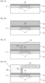
- FIGS. 1 A to 1 C show an exemplary embodiment of the method to form a planarized etch-stop layer, ESL, for a hydrofluoric acid, HF, vapor phase etching process.
- ESL etch-stop layer
- the planarization of the first layer is realized by chemical-mechanical planarization, CMP, for instance.
- CMP chemical-mechanical planarization
- the embodiment employs an additional ESL for CMP process.
- the additional ESL is made of a CMP ESL material 21 , which is deposited on top of exposed parts of a top surface of a substrate, not shown, and a structured first material.
- the first material is a metallic material 20 which forms bottom electrodes.
- the CMP ESL material 21 may for example be SiN, in particular silicon-rich SiN and has a low etch rate regarding CMP etching.
- the metallic material 20 may for example be composed of Ti, TiN, AlCu and/or TiTiN.
- a filling material 22 is deposited on top of the CMP ESL material 21 , in particular to fill gaps in the layer comprising the metallic material 20 .
- the filling material 22 may be a dielectric material, for example SiO2.
- FIG. 1 B shows a first planarized layer after performing CMP, which was suspended with reaching the additional ESL made off the CMP ESL material 21 .
- CMP aims at planarizing the surface it is applied to, a topography of the structure, in particular after deposition of the filling material 22 is not critical.
- FIG. 1 C shows the application of the ESL material 23 forming the intended planarized ESL on top of the planarized first layer.
- the ESL material 23 may be SiN, in particular silicon-rich SiN, which has a low etch rate regarding HF etchants.
- the employment of an additional ESL for the CMP may be optional.
- FIGS. 2 A to 2 C show a variation of the embodiment described in FIGS. 1 A to 1 C .
- the CMP ESL material 21 is patterned and structured together with the metallic material 20 before depositing the filling material 22 .
- the CMP ESL material 21 may act as a mask, hence eliminating the necessity for a resist, for instance, to pattern and structure the metallic material 20 before applying the CMP ESL material 21 , as shown in FIGS. 1 A to 1 C .
- the CMP process also in this variation suspends with reaching the CMP ESL material 21 and therefore forms the first planarized layer, as shown in FIG. 2 B .
- FIG. 2 C consequently shows the deposition of the ESL material 23 for the formation of the planarized ESL.
- FIGS. 3 A to 3 D illustrate a variation of the process as an alternative embodiment of the method according to the improved concept. Compared to the embodiments described in FIGS. 1 A to 1 C and FIGS. 2 A to 2 C , the first material and the second material are exchanged.
- the filling material 22 is deposited as the first material on a surface of the substrate and subsequently patterned and structured, as shown in FIG. 3 A .
- FIG. 3 B shows the deposition of the metallic material 20 as the second material, defining bottom electrodes in the layer of the filling material 22 .
- the filling material 22 can in this case be chosen to have a low etch rate regarding CMP, such that the planarization of the first layer suspends with reaching the filling material 22 , as illustrated in FIG. 3 C .
- FIG. 3 D shows the structure after depositing the ESL material 23 to form the planarized ESL.
- FIGS. 4 A to 4 C show an alternative embodiment of the method to form the planarized ESL on top of the planarized first layer.
- the metallic material 20 is patterned and structured as the first material together with a sacrificial material 25 , as shown in FIG. 4 A .
- the sacrificial material 25 may for example be a resist material that is not removed after structuring the metallic material 20 .
- the patterning and structuring of the metallic material 20 and the sacrificial material 25 for example is realized via a tapered plasma process, in particular to achieve tapered sidewalls 26 of the sacrificial material 25 .
- FIG. 4 B shows the deposition of the filling material 22 as the second material, which can be well-controlled in particular for filling gaps in the first layer comprising the metallic material 20 , such that a thickness of the filling material 22 corresponds to the thickness of the metallic material 20 .
- FIG. 4 C shows the result after removal of the sacrificial material 25 through a lift-off process, for instance, forming the planarized first layer as basis for the planarized ESL of the ESL material 23 on top of the first layer.
- FIGS. 5 A to 5 C show a reversed process as alternative embodiment of the method shown in FIGS. 4 A to 4 C , in which the first material and the second material are exchanged.
- the principle of this embodiment is analogous to the process shown in FIGS. 3 A to 3 D , wherein in a first step the filling material 22 is patterned and structured as the first material together with a sacrificial material 25 on top of the filling material 22 , as shown in FIG. 5 A .
- the sacrificial material 25 may for example be a resist material that is not removed after structuring the filling material 22 .
- FIG. 5 B shows the structure after deposition of the metallic material 20 as the second material in particular on exposed parts of the surface of the substrate, such that the thickness of the metallic material 20 corresponds to the thickness of the filling material 22 .
- FIG. 5 C shows the result after removal of the sacrificial material 25 through a lift-off process, for instance, forming the planarized first layer as basis for the planarized ESL of the ESL material 23 on top of the first layer.
- FIGS. 6 A to 6 D show a further alternative embodiment of the method to form the planarized ESL on top of the planarized first layer.
- the filling material 22 in this embodiment is deposited on the structured metallic material 20 and exposed parts of the surface of the substrate, in particular to fill gaps in the layer comprising the metallic material 20 , as shown in FIG. 6 A .
- FIG. 6 B shows the deposition of an additional material 24 on top of the filling material 22 such that the top surface of the additional material 24 is planar.
- the additional material may be a resist which is applied with a planar top surface via spin-coating, for instance.
- FIG. 6 C shows the planarized first layer after non-selective plasma etching.
- This etching intends to etch the filling material 22 as well as the additional material 24 with similar, in particular equal, rates in order to achieve a planarized surface of the first layer.
- the plasma etch can be well-controlled such that an overetch is prevented.
- FIG. 6 D again shows the structure after depositing the ESL material 23 to form the planarized ESL on top of the planarized first layer.
- FIGS. 7 A to 7 D show exemplary steps after forming the planarized ESL for fabricating a MEMS sensor comprising a planarized ESL.
- FIG. 7 A shows the planarized ESL 13 of the ESL material 23 on top of the planarized first layer comprising bottom electrodes 11 of the metallic material 20 and filling material 22 in gaps between the bottom electrodes 11 .
- the first layer is arranged on top of a surface of a substrate 10 , for example a CMOS substrate with vias in the passivation for electrical connections.
- FIG. 7 B shows the structure after deposition of a planarized sacrificial layer 16 of a further material.
- the further material has a high etch rate compared to the ESL material 23 regarding an HF vapor phase etchant.
- the further material may be the same as the filling material 22 , in particular SiO2.
- SiO2 is characterized by a high selectivity over SiN regarding a HF etchant.
- SiN, in particular silicon-rich SiN is a suitable ESL material 23 .
- FIG. 7 C shows a trench 14 inside the sacrificial layer 16 .
- This trench is filled with a conductive anchor material, for example a metallic material, before a planarized metallic layer 12 of a second metallic material is deposited on top of the sacrificial layer 16 .
- a conductive anchor material for example a metallic material
- the sacrificial layer 16 is removed through a HF vapor phase etching process that suspends the top electrodes 15 , now forming a suspended membrane, as shown in FIG. 7 D .
- the planarized ESL 13 acts as a barrier for the HF etch and hence stops the etching process without influencing the subjacent bottom electrodes 11 , filling material 22 and the substrate 10 .
- a seal layer 26 is deposited to protect the top electrodes 15 and serve as final passivation.
- the exemplary capacitive sensor 1 fabricated following this embodiment of the method according to the improved concept is a specific example and may for example be a pressure sensor.
- the method can be applied to similar sensor manufacturing processes, in which a planar and thin ESL is desired. This is particularly the case if the ESL remains on the finished sensor and a significant decrease of, for example, electrical properties is to be prevented.
Landscapes
- Engineering & Computer Science (AREA)
- Manufacturing & Machinery (AREA)
- Microelectronics & Electronic Packaging (AREA)
- Pressure Sensors (AREA)
- Micromachines (AREA)
Abstract
Description
Claims (14)
Applications Claiming Priority (4)
| Application Number | Priority Date | Filing Date | Title |
|---|---|---|---|
| EP18173267.8 | 2018-05-18 | ||
| EP18173267 | 2018-05-18 | ||
| EP18173267.8A EP3569568B1 (en) | 2018-05-18 | 2018-05-18 | Method for manufacturing an etch stop layer and mems sensor comprising an etch stop layer |
| PCT/EP2019/061823 WO2019219479A1 (en) | 2018-05-18 | 2019-05-08 | Method for manufacturing an etch stop layer and mems sensor comprising an etch stop layer |
Publications (2)
| Publication Number | Publication Date |
|---|---|
| US20210214216A1 US20210214216A1 (en) | 2021-07-15 |
| US11572271B2 true US11572271B2 (en) | 2023-02-07 |
Family
ID=62222407
Family Applications (1)
| Application Number | Title | Priority Date | Filing Date |
|---|---|---|---|
| US17/056,201 Active US11572271B2 (en) | 2018-05-18 | 2019-05-08 | Method for manufacturing an etch stop layer and MEMS sensor comprising an etch stop layer |
Country Status (5)
| Country | Link |
|---|---|
| US (1) | US11572271B2 (en) |
| EP (1) | EP3569568B1 (en) |
| CN (1) | CN112512958B (en) |
| TW (1) | TWI803632B (en) |
| WO (1) | WO2019219479A1 (en) |
Families Citing this family (2)
| Publication number | Priority date | Publication date | Assignee | Title |
|---|---|---|---|---|
| US11211254B2 (en) * | 2019-12-19 | 2021-12-28 | Stmicroelectronics Pte Ltd | Process for integrated circuit fabrication using a buffer layer as a stop for chemical mechanical polishing of a coupled dielectric oxide layer |
| CN112614810A (en) * | 2020-12-18 | 2021-04-06 | 江苏能华微电子科技发展有限公司 | Method and device for flattening metal lamination |
Citations (13)
| Publication number | Priority date | Publication date | Assignee | Title |
|---|---|---|---|---|
| US5789264A (en) * | 1996-03-27 | 1998-08-04 | Daewoo Electronics Co., Ltd. | Method for manufacturing a thin film actuated mirror having a flat light reflecting surface |
| US6203715B1 (en) * | 1999-01-19 | 2001-03-20 | Daewoo Electronics Co., Ltd. | Method for the manufacture of a thin film actuated mirror array |
| US20040092059A1 (en) | 2002-11-05 | 2004-05-13 | Semiconductor Energy Laboratory Co., Ltd. | Semiconductor device and fabricating method thereof |
| US20070057305A1 (en) | 2005-09-13 | 2007-03-15 | Taiwan Semiconductor Manufacturing Company, Ltd. | MIM capacitor integrated into the damascene structure and method of making thereof |
| US20100320548A1 (en) | 2009-06-18 | 2010-12-23 | Analog Devices, Inc. | Silicon-Rich Nitride Etch Stop Layer for Vapor HF Etching in MEMS Device Fabrication |
| US20140231937A1 (en) * | 2011-10-28 | 2014-08-21 | Stmicroelectronics S.R.L. | Method for manufacturing a protective layer against hf etching, semiconductor device provided with the protective layer and method for manufacturing the semiconductor device |
| US20150022431A1 (en) * | 2013-03-11 | 2015-01-22 | Rashed Mahameed | Stress tolerant mems accelerometer |
| US9059259B2 (en) | 2013-07-19 | 2015-06-16 | Taiwan Semiconductor Manufacturing Company Limited | Hard mask for back-end-of-line (BEOL) interconnect structure |
| US20160023893A1 (en) * | 2014-07-28 | 2016-01-28 | Ams International Ag | Suspended membrane for capacitive pressure sensor |
| US9659864B2 (en) | 2015-10-20 | 2017-05-23 | Taiwan Semiconductor Manufacturing Company, Ltd. | Method and apparatus for forming self-aligned via with selectively deposited etching stop layer |
| US9679850B2 (en) | 2015-10-30 | 2017-06-13 | Taiwan Semiconductor Manufacturing Company Ltd. | Method of fabricating semiconductor structure |
| US9726561B2 (en) | 2013-05-20 | 2017-08-08 | Ams International Ag | Differential pressure sensor with a capacitive read out system |
| EP3650826A1 (en) | 2018-11-07 | 2020-05-13 | ams International AG | Semiconductor transducer device with multilayer diaphragm and method of manufacturing a semiconductor transducer device with multilayer diaphragm |
Family Cites Families (2)
| Publication number | Priority date | Publication date | Assignee | Title |
|---|---|---|---|---|
| US6777258B1 (en) * | 2002-06-28 | 2004-08-17 | Silicon Light Machines, Inc. | Conductive etch stop for etching a sacrificial layer |
| US9663346B1 (en) * | 2016-02-17 | 2017-05-30 | Globalfoundries Inc. | MEMs-based resonant FinFET |
-
2018
- 2018-05-18 EP EP18173267.8A patent/EP3569568B1/en active Active
-
2019
- 2019-05-03 TW TW108115388A patent/TWI803632B/en active
- 2019-05-08 US US17/056,201 patent/US11572271B2/en active Active
- 2019-05-08 WO PCT/EP2019/061823 patent/WO2019219479A1/en not_active Ceased
- 2019-05-08 CN CN201980030507.2A patent/CN112512958B/en active Active
Patent Citations (14)
| Publication number | Priority date | Publication date | Assignee | Title |
|---|---|---|---|---|
| US5789264A (en) * | 1996-03-27 | 1998-08-04 | Daewoo Electronics Co., Ltd. | Method for manufacturing a thin film actuated mirror having a flat light reflecting surface |
| US6203715B1 (en) * | 1999-01-19 | 2001-03-20 | Daewoo Electronics Co., Ltd. | Method for the manufacture of a thin film actuated mirror array |
| US20040092059A1 (en) | 2002-11-05 | 2004-05-13 | Semiconductor Energy Laboratory Co., Ltd. | Semiconductor device and fabricating method thereof |
| US20070057305A1 (en) | 2005-09-13 | 2007-03-15 | Taiwan Semiconductor Manufacturing Company, Ltd. | MIM capacitor integrated into the damascene structure and method of making thereof |
| US20100320548A1 (en) | 2009-06-18 | 2010-12-23 | Analog Devices, Inc. | Silicon-Rich Nitride Etch Stop Layer for Vapor HF Etching in MEMS Device Fabrication |
| US20160130140A1 (en) | 2011-10-28 | 2016-05-12 | Stmicroelectronics S.R.L. | Method for manufacturing a protective layer against hf etching, semiconductor device provided with the protective layer and method for manufacturing the semiconductor device |
| US20140231937A1 (en) * | 2011-10-28 | 2014-08-21 | Stmicroelectronics S.R.L. | Method for manufacturing a protective layer against hf etching, semiconductor device provided with the protective layer and method for manufacturing the semiconductor device |
| US20150022431A1 (en) * | 2013-03-11 | 2015-01-22 | Rashed Mahameed | Stress tolerant mems accelerometer |
| US9726561B2 (en) | 2013-05-20 | 2017-08-08 | Ams International Ag | Differential pressure sensor with a capacitive read out system |
| US9059259B2 (en) | 2013-07-19 | 2015-06-16 | Taiwan Semiconductor Manufacturing Company Limited | Hard mask for back-end-of-line (BEOL) interconnect structure |
| US20160023893A1 (en) * | 2014-07-28 | 2016-01-28 | Ams International Ag | Suspended membrane for capacitive pressure sensor |
| US9659864B2 (en) | 2015-10-20 | 2017-05-23 | Taiwan Semiconductor Manufacturing Company, Ltd. | Method and apparatus for forming self-aligned via with selectively deposited etching stop layer |
| US9679850B2 (en) | 2015-10-30 | 2017-06-13 | Taiwan Semiconductor Manufacturing Company Ltd. | Method of fabricating semiconductor structure |
| EP3650826A1 (en) | 2018-11-07 | 2020-05-13 | ams International AG | Semiconductor transducer device with multilayer diaphragm and method of manufacturing a semiconductor transducer device with multilayer diaphragm |
Non-Patent Citations (3)
| Title |
|---|
| International Search Report and Written Opinion dated Jul. 23, 2019 in PCT Application No. PCT/EP2019/061823, 10 pages. |
| Taiwanese Examination Report (with English Translation) in Taiwanese Application No. 108115388 dated Aug. 23, 2022, 20 pages. |
| Taiwanese Office Action (with English Translation) in corresponding Taiwanese Application No. 1108115388 dated Nov. 17, 2022, 12 pages. |
Also Published As
| Publication number | Publication date |
|---|---|
| CN112512958A (en) | 2021-03-16 |
| CN112512958B (en) | 2024-09-17 |
| US20210214216A1 (en) | 2021-07-15 |
| TW202004909A (en) | 2020-01-16 |
| WO2019219479A1 (en) | 2019-11-21 |
| EP3569568A1 (en) | 2019-11-20 |
| EP3569568B1 (en) | 2023-08-02 |
| TWI803632B (en) | 2023-06-01 |
Similar Documents
| Publication | Publication Date | Title |
|---|---|---|
| JP4603740B2 (en) | Precision mechanical structural element and manufacturing method thereof | |
| US7785481B2 (en) | Method for fabricating micromachined structures | |
| US8551798B2 (en) | Microstructure with an enhanced anchor | |
| CN106044701B (en) | Method for producing a microelectromechanical structure in a layer sequence and corresponding electronic component having a microelectromechanical structure | |
| US7932118B2 (en) | Method of producing mechanical components of MEMS or NEMS structures made of monocrystalline silicon | |
| JP5794742B2 (en) | Microelectromechanical system (MEMS) with gap stop and method therefor | |
| JP5474805B2 (en) | Method for manufacturing a MEMS device on a substrate | |
| US10800649B2 (en) | Planar processing of suspended microelectromechanical systems (MEMS) devices | |
| US9499399B2 (en) | Method for forming MEMS structure with an etch stop layer buried within inter-dielectric layer | |
| US6794271B2 (en) | Method for fabricating a microelectromechanical system (MEMS) device using a pre-patterned bridge | |
| US11572271B2 (en) | Method for manufacturing an etch stop layer and MEMS sensor comprising an etch stop layer | |
| US11946822B2 (en) | Semiconductor transducer device with multilayer diaphragm and method of manufacturing a semiconductor transducer device with multilayer diaphragm | |
| CN104649214B (en) | Contact plunger of MEMS and forming method thereof | |
| JP6331552B2 (en) | MEMS device and manufacturing method thereof | |
| US11878906B2 (en) | Method for manufacturing an integrated MEMS transducer device and integrated MEMS transducer device | |
| US20180170748A1 (en) | Semiconductor devices with cavities and methods for fabricating semiconductor devices with cavities | |
| US20160289064A1 (en) | Thin Film Encapsulation of Electrodes |
Legal Events
| Date | Code | Title | Description |
|---|---|---|---|
| AS | Assignment |
Owner name: AMS AG, AUSTRIA Free format text: ASSIGNMENT OF ASSIGNORS INTEREST;ASSIGNORS:FAES, ALESSANDRO;GUILLEMIN, SOPHIE;SIEGERT, JOERG;AND OTHERS;SIGNING DATES FROM 20200817 TO 20201013;REEL/FRAME:054391/0452 |
|
| FEPP | Fee payment procedure |
Free format text: ENTITY STATUS SET TO UNDISCOUNTED (ORIGINAL EVENT CODE: BIG.); ENTITY STATUS OF PATENT OWNER: LARGE ENTITY |
|
| STPP | Information on status: patent application and granting procedure in general |
Free format text: APPLICATION DISPATCHED FROM PREEXAM, NOT YET DOCKETED |
|
| STPP | Information on status: patent application and granting procedure in general |
Free format text: DOCKETED NEW CASE - READY FOR EXAMINATION |
|
| STPP | Information on status: patent application and granting procedure in general |
Free format text: NON FINAL ACTION MAILED |
|
| STPP | Information on status: patent application and granting procedure in general |
Free format text: RESPONSE TO NON-FINAL OFFICE ACTION ENTERED AND FORWARDED TO EXAMINER |
|
| STPP | Information on status: patent application and granting procedure in general |
Free format text: FINAL REJECTION MAILED |
|
| STPP | Information on status: patent application and granting procedure in general |
Free format text: RESPONSE AFTER FINAL ACTION FORWARDED TO EXAMINER |
|
| STPP | Information on status: patent application and granting procedure in general |
Free format text: NOTICE OF ALLOWANCE MAILED -- APPLICATION RECEIVED IN OFFICE OF PUBLICATIONS |
|
| STPP | Information on status: patent application and granting procedure in general |
Free format text: PUBLICATIONS -- ISSUE FEE PAYMENT VERIFIED |
|
| STPP | Information on status: patent application and granting procedure in general |
Free format text: WITHDRAW FROM ISSUE AWAITING ACTION |
|
| STPP | Information on status: patent application and granting procedure in general |
Free format text: NOTICE OF ALLOWANCE MAILED -- APPLICATION RECEIVED IN OFFICE OF PUBLICATIONS |
|
| STPP | Information on status: patent application and granting procedure in general |
Free format text: PUBLICATIONS -- ISSUE FEE PAYMENT VERIFIED |
|
| STCF | Information on status: patent grant |
Free format text: PATENTED CASE |