US11570909B2 - Flexible display apparatus and method of manufacturing the same - Google Patents
Flexible display apparatus and method of manufacturing the same Download PDFInfo
- Publication number
- US11570909B2 US11570909B2 US16/904,388 US202016904388A US11570909B2 US 11570909 B2 US11570909 B2 US 11570909B2 US 202016904388 A US202016904388 A US 202016904388A US 11570909 B2 US11570909 B2 US 11570909B2
- Authority
- US
- United States
- Prior art keywords
- adhesive
- layer
- sub
- flexible display
- display apparatus
- Prior art date
- Legal status (The legal status is an assumption and is not a legal conclusion. Google has not performed a legal analysis and makes no representation as to the accuracy of the status listed.)
- Active, expires
Links
Images


Classifications
-
- H—ELECTRICITY
- H05—ELECTRIC TECHNIQUES NOT OTHERWISE PROVIDED FOR
- H05K—PRINTED CIRCUITS; CASINGS OR CONSTRUCTIONAL DETAILS OF ELECTRIC APPARATUS; MANUFACTURE OF ASSEMBLAGES OF ELECTRICAL COMPONENTS
- H05K5/00—Casings, cabinets or drawers for electric apparatus
- H05K5/0017—Casings, cabinets or drawers for electric apparatus with operator interface units
-
- G—PHYSICS
- G09—EDUCATION; CRYPTOGRAPHY; DISPLAY; ADVERTISING; SEALS
- G09F—DISPLAYING; ADVERTISING; SIGNS; LABELS OR NAME-PLATES; SEALS
- G09F9/00—Indicating arrangements for variable information in which the information is built-up on a support by selection or combination of individual elements
- G09F9/30—Indicating arrangements for variable information in which the information is built-up on a support by selection or combination of individual elements in which the desired character or characters are formed by combining individual elements
- G09F9/301—Indicating arrangements for variable information in which the information is built-up on a support by selection or combination of individual elements in which the desired character or characters are formed by combining individual elements flexible foldable or roll-able electronic displays, e.g. thin LCD, OLED
-
- B—PERFORMING OPERATIONS; TRANSPORTING
- B32—LAYERED PRODUCTS
- B32B—LAYERED PRODUCTS, i.e. PRODUCTS BUILT-UP OF STRATA OF FLAT OR NON-FLAT, e.g. CELLULAR OR HONEYCOMB, FORM
- B32B17/00—Layered products essentially comprising sheet glass, or glass, slag, or like fibres
- B32B17/06—Layered products essentially comprising sheet glass, or glass, slag, or like fibres comprising glass as the main or only constituent of a layer, next to another layer of a specific material
-
- B—PERFORMING OPERATIONS; TRANSPORTING
- B32—LAYERED PRODUCTS
- B32B—LAYERED PRODUCTS, i.e. PRODUCTS BUILT-UP OF STRATA OF FLAT OR NON-FLAT, e.g. CELLULAR OR HONEYCOMB, FORM
- B32B27/00—Layered products comprising a layer of synthetic resin
- B32B27/06—Layered products comprising a layer of synthetic resin as the main or only constituent of a layer, which is next to another layer of the same or of a different material
- B32B27/08—Layered products comprising a layer of synthetic resin as the main or only constituent of a layer, which is next to another layer of the same or of a different material of synthetic resin
-
- B—PERFORMING OPERATIONS; TRANSPORTING
- B32—LAYERED PRODUCTS
- B32B—LAYERED PRODUCTS, i.e. PRODUCTS BUILT-UP OF STRATA OF FLAT OR NON-FLAT, e.g. CELLULAR OR HONEYCOMB, FORM
- B32B27/00—Layered products comprising a layer of synthetic resin
- B32B27/28—Layered products comprising a layer of synthetic resin comprising synthetic resins not wholly covered by any one of the sub-groups B32B27/30 - B32B27/42
- B32B27/281—Layered products comprising a layer of synthetic resin comprising synthetic resins not wholly covered by any one of the sub-groups B32B27/30 - B32B27/42 comprising polyimides
-
- B—PERFORMING OPERATIONS; TRANSPORTING
- B32—LAYERED PRODUCTS
- B32B—LAYERED PRODUCTS, i.e. PRODUCTS BUILT-UP OF STRATA OF FLAT OR NON-FLAT, e.g. CELLULAR OR HONEYCOMB, FORM
- B32B27/00—Layered products comprising a layer of synthetic resin
- B32B27/36—Layered products comprising a layer of synthetic resin comprising polyesters
-
- B—PERFORMING OPERATIONS; TRANSPORTING
- B32—LAYERED PRODUCTS
- B32B—LAYERED PRODUCTS, i.e. PRODUCTS BUILT-UP OF STRATA OF FLAT OR NON-FLAT, e.g. CELLULAR OR HONEYCOMB, FORM
- B32B37/00—Methods or apparatus for laminating, e.g. by curing or by ultrasonic bonding
- B32B37/12—Methods or apparatus for laminating, e.g. by curing or by ultrasonic bonding characterised by using adhesives
-
- B—PERFORMING OPERATIONS; TRANSPORTING
- B32—LAYERED PRODUCTS
- B32B—LAYERED PRODUCTS, i.e. PRODUCTS BUILT-UP OF STRATA OF FLAT OR NON-FLAT, e.g. CELLULAR OR HONEYCOMB, FORM
- B32B7/00—Layered products characterised by the relation between layers; Layered products characterised by the relative orientation of features between layers, or by the relative values of a measurable parameter between layers, i.e. products comprising layers having different physical, chemical or physicochemical properties; Layered products characterised by the interconnection of layers
- B32B7/04—Interconnection of layers
- B32B7/12—Interconnection of layers using interposed adhesives or interposed materials with bonding properties
-
- H01L51/0097—
-
- H01L51/56—
-
- H—ELECTRICITY
- H10—SEMICONDUCTOR DEVICES; ELECTRIC SOLID-STATE DEVICES NOT OTHERWISE PROVIDED FOR
- H10K—ORGANIC ELECTRIC SOLID-STATE DEVICES
- H10K59/00—Integrated devices, or assemblies of multiple devices, comprising at least one organic light-emitting element covered by group H10K50/00
- H10K59/10—OLED displays
- H10K59/12—Active-matrix OLED [AMOLED] displays
- H10K59/1201—Manufacture or treatment
-
- H—ELECTRICITY
- H10—SEMICONDUCTOR DEVICES; ELECTRIC SOLID-STATE DEVICES NOT OTHERWISE PROVIDED FOR
- H10K—ORGANIC ELECTRIC SOLID-STATE DEVICES
- H10K71/00—Manufacture or treatment specially adapted for the organic devices covered by this subclass
-
- H—ELECTRICITY
- H10—SEMICONDUCTOR DEVICES; ELECTRIC SOLID-STATE DEVICES NOT OTHERWISE PROVIDED FOR
- H10K—ORGANIC ELECTRIC SOLID-STATE DEVICES
- H10K71/00—Manufacture or treatment specially adapted for the organic devices covered by this subclass
- H10K71/40—Thermal treatment, e.g. annealing in the presence of a solvent vapour
-
- H—ELECTRICITY
- H10—SEMICONDUCTOR DEVICES; ELECTRIC SOLID-STATE DEVICES NOT OTHERWISE PROVIDED FOR
- H10K—ORGANIC ELECTRIC SOLID-STATE DEVICES
- H10K77/00—Constructional details of devices covered by this subclass and not covered by groups H10K10/80, H10K30/80, H10K50/80 or H10K59/80
- H10K77/10—Substrates, e.g. flexible substrates
- H10K77/111—Flexible substrates
-
- B—PERFORMING OPERATIONS; TRANSPORTING
- B32—LAYERED PRODUCTS
- B32B—LAYERED PRODUCTS, i.e. PRODUCTS BUILT-UP OF STRATA OF FLAT OR NON-FLAT, e.g. CELLULAR OR HONEYCOMB, FORM
- B32B37/00—Methods or apparatus for laminating, e.g. by curing or by ultrasonic bonding
- B32B37/12—Methods or apparatus for laminating, e.g. by curing or by ultrasonic bonding characterised by using adhesives
- B32B2037/1253—Methods or apparatus for laminating, e.g. by curing or by ultrasonic bonding characterised by using adhesives curable adhesive
-
- B—PERFORMING OPERATIONS; TRANSPORTING
- B32—LAYERED PRODUCTS
- B32B—LAYERED PRODUCTS, i.e. PRODUCTS BUILT-UP OF STRATA OF FLAT OR NON-FLAT, e.g. CELLULAR OR HONEYCOMB, FORM
- B32B2255/00—Coating on the layer surface
- B32B2255/10—Coating on the layer surface on synthetic resin layer or on natural or synthetic rubber layer
-
- B—PERFORMING OPERATIONS; TRANSPORTING
- B32—LAYERED PRODUCTS
- B32B—LAYERED PRODUCTS, i.e. PRODUCTS BUILT-UP OF STRATA OF FLAT OR NON-FLAT, e.g. CELLULAR OR HONEYCOMB, FORM
- B32B2255/00—Coating on the layer surface
- B32B2255/20—Inorganic coating
-
- B—PERFORMING OPERATIONS; TRANSPORTING
- B32—LAYERED PRODUCTS
- B32B—LAYERED PRODUCTS, i.e. PRODUCTS BUILT-UP OF STRATA OF FLAT OR NON-FLAT, e.g. CELLULAR OR HONEYCOMB, FORM
- B32B2307/00—Properties of the layers or laminate
- B32B2307/40—Properties of the layers or laminate having particular optical properties
- B32B2307/412—Transparent
-
- B—PERFORMING OPERATIONS; TRANSPORTING
- B32—LAYERED PRODUCTS
- B32B—LAYERED PRODUCTS, i.e. PRODUCTS BUILT-UP OF STRATA OF FLAT OR NON-FLAT, e.g. CELLULAR OR HONEYCOMB, FORM
- B32B2307/00—Properties of the layers or laminate
- B32B2307/70—Other properties
- B32B2307/748—Releasability
-
- B—PERFORMING OPERATIONS; TRANSPORTING
- B32—LAYERED PRODUCTS
- B32B—LAYERED PRODUCTS, i.e. PRODUCTS BUILT-UP OF STRATA OF FLAT OR NON-FLAT, e.g. CELLULAR OR HONEYCOMB, FORM
- B32B2457/00—Electrical equipment
- B32B2457/20—Displays, e.g. liquid crystal displays, plasma displays
-
- B—PERFORMING OPERATIONS; TRANSPORTING
- B32—LAYERED PRODUCTS
- B32B—LAYERED PRODUCTS, i.e. PRODUCTS BUILT-UP OF STRATA OF FLAT OR NON-FLAT, e.g. CELLULAR OR HONEYCOMB, FORM
- B32B2457/00—Electrical equipment
- B32B2457/20—Displays, e.g. liquid crystal displays, plasma displays
- B32B2457/206—Organic displays, e.g. OLED
-
- B—PERFORMING OPERATIONS; TRANSPORTING
- B32—LAYERED PRODUCTS
- B32B—LAYERED PRODUCTS, i.e. PRODUCTS BUILT-UP OF STRATA OF FLAT OR NON-FLAT, e.g. CELLULAR OR HONEYCOMB, FORM
- B32B2457/00—Electrical equipment
- B32B2457/20—Displays, e.g. liquid crystal displays, plasma displays
- B32B2457/208—Touch screens
-
- H01L2251/5338—
-
- H01L27/3244—
-
- H—ELECTRICITY
- H10—SEMICONDUCTOR DEVICES; ELECTRIC SOLID-STATE DEVICES NOT OTHERWISE PROVIDED FOR
- H10K—ORGANIC ELECTRIC SOLID-STATE DEVICES
- H10K2102/00—Constructional details relating to the organic devices covered by this subclass
- H10K2102/301—Details of OLEDs
- H10K2102/311—Flexible OLED
-
- H—ELECTRICITY
- H10—SEMICONDUCTOR DEVICES; ELECTRIC SOLID-STATE DEVICES NOT OTHERWISE PROVIDED FOR
- H10K—ORGANIC ELECTRIC SOLID-STATE DEVICES
- H10K59/00—Integrated devices, or assemblies of multiple devices, comprising at least one organic light-emitting element covered by group H10K50/00
- H10K59/10—OLED displays
- H10K59/12—Active-matrix OLED [AMOLED] displays
- H10K59/122—Pixel-defining structures or layers, e.g. banks
-
- Y—GENERAL TAGGING OF NEW TECHNOLOGICAL DEVELOPMENTS; GENERAL TAGGING OF CROSS-SECTIONAL TECHNOLOGIES SPANNING OVER SEVERAL SECTIONS OF THE IPC; TECHNICAL SUBJECTS COVERED BY FORMER USPC CROSS-REFERENCE ART COLLECTIONS [XRACs] AND DIGESTS
- Y02—TECHNOLOGIES OR APPLICATIONS FOR MITIGATION OR ADAPTATION AGAINST CLIMATE CHANGE
- Y02E—REDUCTION OF GREENHOUSE GAS [GHG] EMISSIONS, RELATED TO ENERGY GENERATION, TRANSMISSION OR DISTRIBUTION
- Y02E10/00—Energy generation through renewable energy sources
- Y02E10/50—Photovoltaic [PV] energy
- Y02E10/549—Organic PV cells
-
- Y—GENERAL TAGGING OF NEW TECHNOLOGICAL DEVELOPMENTS; GENERAL TAGGING OF CROSS-SECTIONAL TECHNOLOGIES SPANNING OVER SEVERAL SECTIONS OF THE IPC; TECHNICAL SUBJECTS COVERED BY FORMER USPC CROSS-REFERENCE ART COLLECTIONS [XRACs] AND DIGESTS
- Y02—TECHNOLOGIES OR APPLICATIONS FOR MITIGATION OR ADAPTATION AGAINST CLIMATE CHANGE
- Y02P—CLIMATE CHANGE MITIGATION TECHNOLOGIES IN THE PRODUCTION OR PROCESSING OF GOODS
- Y02P70/00—Climate change mitigation technologies in the production process for final industrial or consumer products
- Y02P70/50—Manufacturing or production processes characterised by the final manufactured product
Definitions
- the present disclosure relates to the field of display technologies, and in particular, to a flexible display apparatus and a method of manufacturing the same.
- the flexible display apparatus includes at least two flexible elements and at least one adhesive layer bonding the at least two flexible elements.
- the flexible display apparatus has a bendable region, each adhesive layer includes a first portion in the bendable region and a second portion, at least part of the second portion is located outside the bendable region.
- the adhesive layer is configured such that at a same temperature, a storage modulus of the first portion is greater than a storage modulus of the second portion.
- a thickness of the first portion is less than or equal to a thickness of the adhesive layer.
- the at least two flexible elements include at least three flexible elements, and the at least one adhesive layer includes a plurality of adhesive layers. Every two adjacent flexible elements are provided with one of the plurality of adhesive layers therebetween.
- an orthographic projection of the first portion on one of the at least two flexible elements and an orthographic projection of the bendable region on the one of the at least two flexible elements coincide.
- the first portion includes a plurality of sub-portions arranged at intervals, and orthographic projections of the plurality of sub-portions on the one of the at least two flexible elements are within the orthographic projection of the bondable region on the one of the at least two flexible elements.
- the plurality of sub-portions are arranged in an array.
- one of the at least one adhesive layer has a single-layer structure and the thickness of the first portion is less than the thickness of the adhesive layer.
- the first portion is located in at least one of an upper half region and a lower half region of the one of the at least one adhesive layer.
- one of the at least one adhesive layer has a multi-layer structure and includes a plurality of adhesive sub-layers that are stacked along a thickness direction of the adhesive layer; and at least one adhesive sub-layer includes the first portion.
- an adhesive sub-layer including the first portion and an adhesive sub-layer not including the first portion are arranged alternately.
- the plurality of adhesive sub-layers include a first adhesive sub-layer and a second adhesive sub-layer that are stacked along the thickness direction of the adhesive layer.
- One of the first adhesive sub-layer and the second adhesive sub-layer includes the first portion, and a sum of thicknesses of the first adhesive sub-layer and the second adhesive sub-layer is less than or equal to approximately 100 microns, and more than or equal to 15 microns.
- the first adhesive sub-layer includes the first portion, a thickness of the first adhesive sub-layer is greater than a thickness of the second adhesive sub-layer, and a thickness of the second adhesive sub-layer is in a range from approximately 5 microns to approximately 15 microns.
- the second adhesive sub-layer includes the first portion, the thickness of the second adhesive sub-layer is greater than the thickness of the first adhesive sub-layer, and the thickness of the first adhesive sub-layer is in a range from approximately 5 microns to approximately 15 microns.
- the first portion is configured such that the storage modulus of the first portion is in a range from approximately 100 KPa to approximately 200 KPa at 25° C.; and the second portion is configured such that the storage modulus of the second portion is in a range from approximately 20 KPa to approximately 100 KPa at 25° C.
- an adhesive strength of the first portion is greater than an adhesive strength of the second portion.
- the adhesive strength of the first portion is in a range from approximately 2000 gf/inch to approximately 4000 gf/inch; and the adhesive strength of the second portion is in a range from approximately 1500 gf/inch to approximately 3000 gf/inch.
- a glass transition temperature of the adhesive layer is less than or equal to ⁇ 30° C., and more than or equal to ⁇ 45° C.
- a light transmittance of the adhesive layer is greater than or equal to approximately 93%, and a haze of the adhesive layer is less than or equal to approximately 1%.
- Some embodiments of the present disclosure provide a method of manufacturing the flexible display apparatus described above.
- the method includes: forming the at least one adhesive layer which includes the first portion; and bonding the at least two flexible elements through the at least one adhesive layer.
- Forming the at least one adhesive layer includes: forming the first portion through curing by using energy irradiation, so that at a same temperature, a storage modulus of the first portion is greater than a storage modulus of the second portion, and a thickness of the first portion is less than or equal to a thickness of the adhesive layer.
- forming the first portion through curing by using energy irradiation includes: forming an optical adhesive film; curing a portion of the optical adhesive film through UV curing, so as to form the first portion.
- curing a portion of the optical adhesive film through UV curing includes: curing the portion of the optical adhesive film through UV curing by using a mask having at least one opening which corresponds to the first portion to be formed in an inert gas atmosphere, so as to form the first portion.
- forming the adhesive layer includes: forming a base material layer; and adding different proportions of photo initiators to a portion of the base material layer corresponding to the first portion to be formed and a portion of the base material layer corresponding to the second portion to be formed.
- the base material layer includes at least one of acrylic resin, polyurethane resin, epoxy polyester resin, or silicone resin.
- the photo initiators include at least one of 1-hydroxycyclohexylphenylketone, benzoin dimethyl ether, 2-hydroxy-2-methylpropiophenone, benzophenone, 2,4,6-trimethylanisole diphenyl phosphine oxide, methyl phenylglyoxylate, phenyl bis (2,4,6-trimethylbenzoyl)-phosphine oxide, or isopropyl thioxanthone.
- forming the adhesive layer includes: forming a first optical adhesive sub-film; curing a portion of the first optical adhesive sub-film corresponding to the first portion to be formed by energy irradiation to form a first adhesive sub-layer including the first portion; and forming a second adhesive sub-layer on the first adhesive sub-layer.
- forming one of the at least one adhesive layer includes: forming a first optical adhesive sub-layer; forming a second optical adhesive sub-film on the first adhesive sub-layer; and curing a portion of the second optical adhesive sub-film corresponding to the first portion to be formed by energy irradiation to form a second adhesive sub-layer including the first portion.
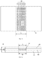
- FIG. 1 A is a schematic sectional view of a flexible display apparatus, according to some embodiments.
- FIG. 1 B is a schematic sectional view of another flexible display apparatus, according to some embodiments.
- FIG. 2 is a schematic top view of a flexible display panel, according to some embodiments.
- FIG. 3 is a schematic sectional view taken along direction A-A′ of the flexible display panel shown in FIG. 2 ;
- FIG. 4 is a schematic top view of a display apparatus, according to some embodiments.
- FIG. 5 is a schematic sectional view taken along direction B-B′ of the display apparatus in FIG. 4 , according to some embodiments;
- FIG. 6 is a schematic top view of another display apparatus, according to some embodiments.
- FIG. 7 is a schematic sectional view taken along direction C-C′ of the display apparatus in FIG. 6 , according to some embodiments;
- FIG. 8 is a schematic sectional view showing a structure of a flexible display apparatus in a bent state, according to the related art
- FIG. 9 is a schematic sectional view of the flexible display apparatus shown in FIG. 8 after it is unfolded, according to the related art.
- FIG. 10 is a schematic top view of another display apparatus, according to some embodiments of the present disclosure.
- FIG. 11 is a schematic top view of yet another display apparatus, according to some embodiments.
- FIG. 12 is a schematic sectional view of an adhesive layer, according to some embodiments.
- FIG. 13 is a schematic sectional view of another adhesive layer, according to some embodiments.
- FIG. 14 is a schematic sectional view showing a structure of yet another adhesive layer, according to some embodiments.
- FIG. 15 is a schematic sectional view of yet another adhesive layer, according to some embodiments.
- FIGS. 16 to 18 are schematic diagrams showing how to form an optical adhesive layer, according to some embodiments.
- FIG. 19 is a schematic diagram showing another way of forming an optical adhesive film on a flexible display panel, according to some embodiments.
- FIG. 20 is a schematic diagram showing how to form another adhesive layer, according to some embodiments.
- FIG. 21 is a schematic diagram showing how to form yet another adhesive layer, according to some embodiments.
- orientations or positional relationships indicated by terms “center”, “upper”, “lower”, “front”, “rear”, “left”, “right”, “vertical”, “horizontal”, “top”, “bottom”, “inner”, “outer”, etc. are based on orientations or positional relationships shown in the drawings, and are merely used to facilitate and simplify the description of the present disclosure, and do not indicate or imply that the referred devices or elements must have a particular orientation, or must be constructed or operated in a particular orientation. Therefore they should not be construed as limitations to the present disclosure.
- a/the plurality of means two or more unless otherwise specified.
- Terms such as “first” and “second” are used for descriptive purposes only, and are not to be construed as indicating or implying the relative importance or implicitly indicating the number of indicated technical features.
- A when A is referred to as being “on” B, it may include the following two situations: (1) A is directly on B, which means there is nothing else between A and B; (2) A is indirectly on B, which means there is at least a C between A and B.
- A, B and C may be a component, a substrate, a frame, a layer or a pattern in a display apparatus.
- “A and/or B” includes the following combinations of A and B: only A, only B, and a combination of A and B.
- the flexible display apparatus includes at least two flexible elements and at least one adhesive layer 4 .
- the at least two flexible elements include a flexible display panel 1 and at least one flexible layer (such as a protective layer 2 ).
- the at least two flexible elements include at least two flexible layers (such as the protective layer 2 and functional layers 3 ).
- the at least one layer means one or more layers, and at least two layers, a plurality of or multiple layers means two or more layers unless otherwise specified.
- the at least one flexible layer includes a protective layer 2 on the flexible display panel 1 .
- the protective layer 2 may be made of a transparent material such as flexible glass, transparent plastic or transparent resin.
- the flexible display panel 1 and the protective layer 2 are bonded by the adhesive layer 4 .
- the at least one flexible layer may further include the functional layers 3 provided between the flexible display panel 1 and the protective layer 2 .
- the functional layers 3 may include multiple layers arranged in a thickness direction of the flexible display apparatus.
- the functional layers 3 include an optical film 31 (such as a polarizer) and a touch layer 32 .
- the flexible display panel 1 and the optical film 31 are bonded by the adhesive layer 4
- the optical film 31 and the touch layer 32 are bonded by the adhesive layer 4
- the touch layer 32 and the protective layer 2 are bonded by the adhesive layer 4 .
- the at least two flexible layers include the protective layer 2 , the optical film 31 and the touch layer 32 .
- the optical film 31 and the touch layer 32 are bonded by the adhesive layer 4
- the touch layer 32 and the protective layer 2 are bonded by the adhesive layer 4 .
- the flexible display panel 1 may be a top-emitting display panel, a bottom-emitting display panel or a double-sided light-emitting display panel.
- the flexible display panel 1 is the top-emitting display panel, and in a direction pointing to the protective layer 2 from the flexible display panel 1 , the functional layers 3 and the protective layer 2 are sequentially arranged on the display side of the flexible display panel 1 .
- FIG. 2 is a schematic top view of a flexible display panel 1 according to some embodiments.
- the flexible display panel 1 includes an active area A and a peripheral area S located on at least one side of the active area A.
- the peripheral area S is arranged to surround the active area A, and the peripheral area S may be in a shape of a ring (e.g., a rectangular ring).
- the shapes of the active area A and the peripheral area S are not limited thereto, and the shape of the peripheral region S may change as the shape of the active area A changes.
- the flexible display panel 1 includes a plurality of sub-pixels P located in the active area A, and the number and arrangement manner of the plurality of sub-pixels P are not limited to the examples shown in the accompanying drawings.
- the flexible display panel 1 may further include electronic components, wires or lines arranged in the peripheral region S.
- the electronic components include driving circuits such as a power IC, a timing control (TCON) IC, a source driver IC and a gate driver IC.
- the flexible display panel 1 may be an electroluminescent display panel or a photoluminescence display panel.
- the electroluminescent display panel may be an organic light-emitting diode (OLED) display panel or a quantum dot light-emitting diode (QLED) display panel.
- OLED organic light-emitting diode
- QLED quantum dot light-emitting diode
- the flexible display panel 1 includes a flexible substrate 11 and the plurality of sub-pixels P on the flexible substrate 11 .
- Each sub-pixel P includes a pixel driving circuit and a light-emitting device 12 .
- the pixel driving circuit includes a plurality of thin film transistors and at least one capacitor.
- the plurality of thin film transistors include a driving transistor 13 and at least one switching transistor. A drain or a source of the driving transistor 13 is electrically connected to an anode 121 of the light-emitting device 12 .
- the pixel driving circuit may have a “2T1C”, “6T1C”, “7T1C”, “6T2C”, or “7T2C” structure.
- T indicates a thin film transistor
- C indicates a capacitor
- the number before “C” indicates the number of the at least one capacitor in the pixel driving circuit.
- the pixel driving circuit with the 2T1C structure includes two thin film transistors and one capacitor.
- the flexible substrate 11 is made of a flexible material.
- the flexible material includes at least one of polyethylene terephthalate (PET), polyethylene naphthalate two formic acid glycol ester (PEN) or a polyimide (PI).
- the flexible display panel 1 further includes a pixel defining layer 14 .
- the pixel defining layer 14 includes a plurality of openings PP, and one light-emitting device 12 corresponds to an opening PP.
- the light-emitting device 12 includes the anode 121 , a cathode 123 and a light-emitting functional layer 122 between the anode 121 and the cathode 123 .
- the light-emitting functional layer 122 includes at least a light-emitting layer.
- the light-emitting functional layer 122 further includes at least one of an electron injection layer (EIL), an electron transporting layer (ETL), a hole transporting layer (HTL) or a hole injection layer (HIL). If the light-emitting function layer 122 includes the EIL, the ETL, the light-emitting layer, the HTL and the HIL, all the layers are stacked sequentially.
- the light-emitting device 12 may be a top-emitting device.
- the anode 121 is opaque.
- the anode 12 may have a multiple-layer structure, and may be composed of at least one indium tin oxide (ITO) layer and at least one silver (Ag) layer.
- ITO indium tin oxide
- Ag silver
- the cathode 123 may be transparent or translucent.
- the cathode 123 is a silver sheet which is thin enough to be transparent or translucent.
- the flexible display panel 1 further includes, for example, a passivation layer 15 and a planarization layer 16 provided between the driving transistor 13 and the anode 121 .
- the flexible display panel 1 may further include an encapsulation layer 17 for encapsulating the light-emitting device 12 .
- the encapsulation layer 17 may be an encapsulation film.
- the flexible display apparatus has a bendable region L.
- the adhesive layer 4 includes a first portion H in the bendable region L, and a second portion. At least part of the second portion is located outside the bendable region L (as shown by the dotted boxes in FIGS. 5 and 7 ).
- the adhesive layer 4 is configured such that at a same temperature, a storage modulus of the first portion H is greater than a storage modulus of the second portion.
- a thickness d 1 of the first portion H is less than or equal to a thickness D of the adhesive layer 4 .
- the storage modulus is a physical quantity used to characterize an ability of a solid material's resistance to deformation.
- a material with a high storage modulus has high rigidity and is difficult to bend or stretch. In addition, it is easier for the material with the high storage modulus to restore to an original state after a force that bends or stretches the material is eliminated.
- the adhesive layer 4 does not include the first portion H
- the adhesive layer 4 has a relatively high storage modulus at any position
- the bendable portion of the flexible display apparatus in the bendable region L may be hard to be bent, which may cause the flexible display apparatus hard to be bent.
- the adhesive layer 4 has a relatively low storage modulus at any position, that is, the adhesive layer 4 has relatively high flexibility at any position, as shown in FIG. 9 , it is difficult for the bendable portion of the flexible display apparatus to restore to the original state after being bent, which may cause unevenness of the flexible display apparatus.
- the adhesive layer 4 includes the first portion H in the bendable region L. Since at the same temperature, the storage modulus of the first portion H is greater than the storage modulus of the second portion, a rigidity of the bendable portion of the flexible display apparatus located in the bendable region L may be improved. As a result, it may be easier for the bendable portion to restore to the original state after being bent.
- organic layers in the flexible display apparatus may generate gas during the deformation process (such as deformation caused by compressive stress) in a high temperature.
- gas when gas is generated in flexible layers bonded to the first portion H (for example, the optical film 31 , the touch layer 32 or the protective layer 2 ), since the rigidity of the first portion H is high and the first portion H is not easily deformed, the generated gas may only be discharged from a peripheral area and may not easily gather to form bubbles. In this way, it may be possible to avoid a problem of bubbles in the bendable region L when the flexible display apparatus is bent in a high temperature.
- the first portion H of the adhesive layer 4 is configured such that the storage modulus of the first portion H is in a range from approximately 100 KPa to approximately 200 KPa at 25° C.
- the second portion of the adhesive layer 4 is configured such that the storage modulus of the second portion is in a range from approximately 20 KPa to approximately 100 KPa at 25° C.
- the storage modulus of the first portion H of the adhesive layer 4 may be 100 KPa, 110 KPa, 120 KPa, 130 KPa, 140 KPa, 150 KPa, 160 KPa, 170 KPa, 180 KPa, 190 KPa or 200 KPa at 25° C.
- the storage modulus of the second portion of the adhesive layer 4 may be 20 KPa, 30 KPa, 40 KPa, 50 KPa, 60 KPa, 70 KPa, 80 KPa, 90 KPa, or 100 KPa at 25° C.
- the storage modulus of the second portion of the adhesive layer 4 is in a range from approximately 30 KPa to approximately 50 KPa at 25° C.
- the storage modulus of the adhesive layer 4 may be measured by using an advanced rheometric expansion system (ARES) or a discovery hybrid rheometer (DHR). During the measurement, a portion of the adhesive layer 4 having a thickness of 1 mm and a diameter of 8 nm is taken as the sample. Besides, an oscillation frequency in the measurement may be 1 Hz and the temperature in the measurement may be 25° C.
- ARES advanced rheometric expansion system
- DHR discovery hybrid rheometer
- the adhesive layer 4 Since the first portion H is only provided in the bendable region L, and the adhesive layer 4 has the second portion with a lower storage modulus relative to the first portion H, the adhesive layer 4 still has a certain flexibility in the second portion. This design is conducive to releasing a stress generated in the first portion H during a bending process. Therefore, a bending stress on the flexible display apparatus during the bending process and a shear stress between layers of the flexible display apparatus may be reduced.
- the adhesive strength increases. Since the storage modulus of the first portion H is greater than that of the second portion, an adhesive strength of the first portion H is greater than that of the second portion. The greater the adhesive strength, the greater the force required to peel off a layer of two layers bonded together.
- the unit of the adhesive strength is gram force per inch (gf/inch).
- an adhesion between the first portion H and an object to which the first portion H is adhered is better than that of the second portion. In this way, while the certain flexibility of the flexible display apparatus is ensured, it is possible to prevent a delamination problem in the bendable region L after a long-term bending of the flexible display apparatus.
- the first portion H and the second portion are formed by photocuring (such as UV curing). For example, by adjusting a content of the photoinitiator, the first portion H and the second portion with different degrees of curing are formed. For example, the first portion H and the second portion with different degrees of curing may be formed by controlling irradiation conditions during the curing process.
- the process of forming the first portion and the second portion is as follows: different proportions of photo initiators are added to a same kind of base material to form a first material and a second material, respectively, the proportion of photoinitiator in the first material being higher than that of the second material; then the first material is cured to form the first portion H with a relatively high degree of curing, and the second material is cured to form the second portion with a relatively low degree of curing. Since the degree of curing of the first portion H is higher than that of the second portion, the first portion H has a greater storage modulus and a greater adhesive strength than the second portion.
- the base material of both the first portion H and the second portion includes at least one of acrylic resin, polyurethane resin, epoxy polyester resin or silicone resin.
- the initiator may be photoinitiator selected from a group consisting of 1-hydroxycyclohexylphenylketone, benzoin dimethyl ether, 2-hydroxy-2-methylpropiophenone benzophenone, 2,4,6-trimethylanisole diphenyl phosphine oxide, methyl phenylglyoxylate, phenyl bis (2,4,6-trimethylbenzoyl)-phosphine oxide, isopropyl thioxanthone and combinations thereof.
- the adhesive strength of the first portion H and the adhesive strength of the second portion are not limited, as long as the adhesive strength of the first portion H is greater than the adhesive strength of the second portion.
- the adhesive strength of the first portion H is in a range from approximately 2000 gf/inch to approximately 4000 gf/inch
- the adhesive strength of the second portion of the adhesive layer 4 is in a range from approximately 1500 gf/inch to approximately 3000 gf/inch.
- the adhesive strength of the first portion H may be 2000 gf/inch, 3000 gf/inch or 4000 gf/inch
- the adhesive strength of the second portion of the adhesive layer 4 may be 1500 gf/inch, 2000 gf/inch, 2500 gf/inch or 3000 gf/inch.
- the adhesive strength of the adhesive layer 4 may be measured by using a tensile testing machine.
- the adhesive layer 4 is made of a transparent adhesive material such as optically clear adhesive (OCA) or optically clear resin (OCR).
- OCA optically clear adhesive
- OCR optically clear resin
- the light transmittance of the adhesive layer 4 is greater than or equal to approximately 93%, and a haze of the adhesive layer 4 is less than or equal to approximately 1%.
- haze is an important parameter of optical transparency of transparent or translucent materials. The higher the haze, the lower the transparency of the transparent or translucent materials, which means poor light transmittance of the transparent or translucent materials.
- a glass transition temperature of the adhesive layer 4 is less than or equal to approximately ⁇ 30° C., and greater than or equal to approximately ⁇ 45° C.
- the glass transition temperature of the adhesive layer 4 is ⁇ 30° C. or ⁇ 40° C.
- the glass transition temperature refers to a temperature at which the adhesive layer 4 transitions between a glassy state and a high-elastic state. With the glass transition temperature as a dividing line, the adhesive layer 4 is in a hard and brittle glassy state below the glass transition temperature, and is in a robbery and high-elastic state above the glass transition temperature. It can be understood that, in order to ensure that the adhesive layer 4 is in a high-elastic state at various possible operating temperatures (for example, when the flexible display apparatus is used in a cold region, the operating temperature may be very low), the glass transition temperature of the adhesive layer needs to be as low as possible.
- the glass transition temperature of the adhesive layer 4 is ⁇ 30° C.
- the adhesive layer 4 has good flexibility.
- orthographic projections of the first portion H and the bendable region L on the flexible display panel 1 coincide.
- the first portion H includes a plurality of sub-portions h arranged at intervals, and orthographic projections of the plurality of sub-portions h on the flexible display panel 1 are within the orthographic projection of the bendable region L on the flexible display panel 1 . That is, the orthographic projection of the first portion H on the flexible display panel 1 partially overlaps with the orthographic projection of the bendable region L on the flexible display panel 1 .
- the plurality of sub-portions h are arranged in an array.
- the plurality of sub-portions h may be randomly arranged, or some of the plurality of sub-portions h are arranged in an array.
- the arrangement of the plurality of sub-portions h is not limited thereto, and can be set according to actual needs.
- an orthographic projection of at least one sub-portion h on the flexible display panel 1 is in a shape of a quadrangle such as a rhombus or a rectangle.
- a quadrangle such as a rhombus or a rectangle.
- an orthographic projection of each sub-portion h on the flexible display panel 1 is in the shape of the rhombus.
- the orthographic projection of each sub-portion h on the flexible display panel 1 is in the shape of the rectangle.
- the orthographic projection of each sub-portion h on the flexible display panel 1 may be in other regular shapes or irregular shapes.
- the adhesive layer 4 may have a single-layer structure or a multi-layer structure. A position of the first portion H in the adhesive layer is different according to whether the adhesive layer 4 has the single-layer structure or the multi-layer structure.
- the adhesive layer 4 has the single-layer structure and the thickness d 1 of the first portion H is less than the thickness D of the adhesive layer 4 .
- the first portion H is located in at least one of an upper half region or a lower half region of the adhesive layer 4 in the bendable region L.
- the first portion H is provided in both of the upper half region and the lower half region of the adhesive layer 4 in the bendable region L. In this way, no matter whether the flexible display apparatus is bent in a direction as shown in FIG. 8 , or in a direction opposite to the direction shown in FIG. 8 , it may be possible to avoid the problem that it is difficult for the bendable portion of the flexible display apparatus to restore to the original state after being bent.
- the first portion H is located in the lower half region of the adhesive layer 4 .
- the adhesive layer 4 has the multi-layer structure and includes a plurality of adhesive sub-layers (for example, a first sub-layer 41 , a second sub-layer 42 and a third sub-layer 43 ) that are stacked on top of one another, and at least one of the plurality of adhesive sub-layers includes the first portion H.
- a plurality of adhesive sub-layers for example, a first sub-layer 41 , a second sub-layer 42 and a third sub-layer 43 .
- FIG. 12 shows a case where only the second adhesive sub-layer 42 includes the first portion H.
- FIG. 13 shows a case where both of the second adhesive sub-layer 42 and the third adhesive sub-layer 43 include the first portions H.
- the adhesive layer 4 includes a plurality of adhesive sub-layers that are stacked on top of one another, and at least one of the plurality of adhesive sub-layers includes the first portion H.
- the first portion H may include a plurality of sub-portions h.
- at least one of the first portions H may include a plurality of sub-portions h.
- At least one adhesive sub-layer that includes the first portion H including a plurality of sub-portions h, and at least one adhesive sub-layer that includes the first portion H not including a plurality of sub-portions h are arranged alternately.
- one adhesive sub-layer that includes the first portion H including a plurality of sub-portions h, and one adhesive sub-layer that includes the first portion H not including a plurality of sub-portions h are arranged alternately.
- two adhesive sub-layers (each of which includes the first portion H including a plurality of sub-portions h) and two adhesive sub-layers (each of which includes the first portion H not including a plurality of sub-portions h) are arranged alternately.
- At least one adhesive sub-layer that includes the first portion H including a plurality of sub-portions h, and at least one adhesive sub-layer that does not include the first portion H are arranged alternately; or, at least one adhesive sub-layer that includes the first portion H not including a plurality of sub-portions h, and at least one adhesive sub-layer that does not include the first portion H are arranged alternately; or, the three kinds of sub-layers are arranged alternately.
- the adhesive layer 4 has a two-layer structure and includes the first adhesive sub-layer 41 and the second adhesive sub-layer 42 that are stacked on top of one another.
- a total thickness D of the first adhesive sub-layer 41 and the second adhesive sub-layer 42 is less than or equal to approximately 100 microns, and greater than or equal to approximately 15 microns. In a case where the adhesive layer with the total thickness D less than or equal to approximately 100 microns and greater than or equal to approximately 15 microns is used in the flexible display apparatus, it may be easy for the flexible display apparatus to realize a folding function.
- the first adhesive sub-layer 41 includes the first portion H, and the thickness of the first adhesive sub-layer 41 is greater than the thickness of the second adhesive sub-layer 42 .
- the thickness of the second adhesive sub-layer 42 may be in a range from approximately 5 microns to approximately 15 microns. In this way, it may be guaranteed that there is enough space in the first adhesive sub-layer 41 to accommodate the first portion H. Therefore, it may be possible to ensure that the bendable portion located in the bendable region L of the flexible display apparatus is rigid enough to make the flexible display apparatus restore to the original state after being bent.
- the thickness of the second adhesive sub-layer 42 may be 5 microns, 7 microns, 9 microns, 11 microns, 13 microns or 15 microns.
- the second adhesive sub-layer 42 includes the first portion H, and the thickness of the second adhesive sub-layer 42 is greater than the thickness of the first adhesive sub-layer 41 .
- the thickness of the first adhesive sub-layer 41 may be in a range from approximately 5 microns to approximately 15 microns. In this way, it may be guaranteed that there is enough space in the second adhesive sub-layer 42 to accommodate the first portion H. Therefore, it may be possible to ensure that the bendable portion located in the bendable region L of the flexible display apparatus is rigid enough to make the flexible display apparatus restore to the original state after being bent.
- the thickness of the first adhesive sub-layer 41 may be 5 microns, 7 microns, 9 microns, 11 microns, 13 microns or 15 microns.
- Some embodiments of the present disclosure provide a method of manufacturing the flexible display apparatus described above, and the method includes the following steps.
- FIGS. 1 B and 5 the at least one adhesive layer 4 which includes the first portion H and the second portion is formed. Then, the at least two flexible elements are bonded through the at least one adhesive layer 4 .
- FIG. 1 B takes at least two flexible elements including the flexible display panel 1 , the protective layer 2 , the optical film 31 and the touch layer 32 as an example.
- one of the at least one the adhesive layer 4 is formed on at least one of the at least two flexible elements (for example, the flexible display panel 1 and the at least one flexible layer; or at least two flexible layers).
- the at least one adhesive layer 4 may be formed on a release liner. In this case, during the bonding of two flexible elements, the adhesive layer 4 is first peeled from the release liner, then the adhesive layer 4 is adhered to one of the two flexible elements, and then the two flexible elements are bonded by the adhesive layer 4 .
- the step of forming the at least one adhesive layer 4 includes forming the first portion H through curing by using energy irradiation. As shown in FIG. 5 , the flexible display apparatus has the bendable region L. The adhesive layer 4 includes the first portion H in the bendable region L.
- the first portion H is formed in at least part of the bendable region L During the formation of the adhesive layer 4 , the first portion H of the adhesive layer 4 is formed through curing by using energy irradiation (such as heat irradiation, light irradiation or radiation irradiation), so that at a same temperature, the storage modulus of the first portion H obtained after curing is greater than the storage modulus of the second portion of the adhesive layer 4 , and a thickness of the first portion H is less than or equal to a thickness of the adhesive layer 4 .
- energy irradiation such as heat irradiation, light irradiation or radiation irradiation
- polymerization of a polymer material containing active functional groups in a material used for forming the adhesive layer 4 may be initiated by, for example, UV light, so as to form the first portion H in the adhesive layer 4 .
- polymerization of the polymer material containing active functional groups in the material used for forming the adhesive layer 4 may be initiated by, for example, an electron beam, so as to form the first portion H.
- forming the first portion H in the adhesive layer 4 through curing by using energy irradiation includes: forming an optical adhesive film 100 on at least one of the flexible display panel 1 and one of the at least one flexible layer; and curing a portion of the optical adhesive film 100 through UV curing by using a mask 200 having at least one opening which corresponds to the first portion to be formed, so as to form the first portion H.
- a region of the optical adhesive film 100 corresponding to the second portion to be formed is shielded by a shielding portion of the mask 200 .
- the region of the optical adhesive film 100 corresponding to the first portion to be formed is exposed by at least one opening of the mask 200 .
- regions of the optical adhesive film 100 corresponding to the first portion to be formed and the second portion to be formed may be treated with different curing conditions, and thus the first portion H may have a different storage modulus from the second portion.
- the rigidity of the first portion H in the flexible display apparatus manufactured by the above method may be improved. Therefore, the rigidity of the bendable portion located in the bendable region L may be improved. As a result, it may be easier for the bendable portion of the flexible display apparatus to restore to the original state after being bent.
- the manufacturing methods thereof may be different.
- the first portion H is formed in at least one of the upper half region and the lower half region of the adhesive layer 4 .
- the method will be described below with reference to FIG. 18 by taking the first portion H located in the upper half region of the adhesive layer 4 as an example. The method includes the following steps.
- an optical adhesive film 100 is formed, for example, on the flexible display panel 1 or on one of the at least one flexible layer (such as the protective layer 2 or the touch layer 32 ).
- forming the optical adhesive film 100 includes: forming a base material layer; and adding different proportions of photo initiators to a portion of the base material layer corresponding to the first portion to be formed and a portion of the base material layer corresponding to the second portion to be formed respectively.
- the base material layer of the optical adhesive film 100 may include at least one of acrylic resin, polyurethane resin, epoxy polyester resin or silicone resin.
- the portions of the optical adhesive film 100 corresponding to the first portion to be formed and the second portion to be formed include the different proportions of photo initiators respectively.
- the proportion of photoinitiator added to the portion corresponding to the first portion to be formed is higher than the proportion of photoinitiator added to the portion corresponding to the second portion to be formed.
- a curing degree of the first portion H formed by the photocuring process may be higher than that of the second portion.
- the storage modulus of the first portion may be greater than the storage modulus of the second portion.
- the photoinitiator may include at least one of 1-hydroxycyclohexylphenylketone, benzoin dimethyl ether, 2-hydroxy-2-methylpropiophenone, benzophenone, 2,4,6-trimethylanisole diphenyl phosphine oxide, methyl phenylglyoxylate, phenyl bis (2,4,6-trimethylbenzoyl)-phosphine oxide, or isopropyl thioxanthone.
- the region of the optical adhesive film 100 corresponding to the first portion to be formed is cured by being irradiated from top to bottom during the photocuring process to form the first portion H in the upper half region of the adhesive film 4 .
- the first optical adhesive slayer 100 is exposed to UV light when being masked by the mask 200 having at least one opening which corresponds to the first portion to be formed.
- the upper surface of the region of the optical adhesive film 100 corresponding to the first portion to be formed is exposed to UV light through a corresponding opening of the mask 200 .
- the thickness of the first portion H may be controlled, and thus the adhesive layer 4 shown in FIG. 18 may be formed.
- the portion of the optical adhesive film 100 is cured through UV curing by using the mask 200 in an inert gas atmosphere, so as to form the first portion H.
- the inert gas may be nitrogen.
- the adhesive layer 4 has a multi-layer structure and includes a plurality of adhesive sub-layers, for example, a first adhesive sub-layer 41 , a second adhesive sub-layer 42 and a third adhesive sub-layer 43 that are stacked on top of one another, the first portion H is formed in at least one of the adhesive sub-layers.
- the adhesive layer 4 is formed on the flexible display panel 1 .
- the adhesive layer includes three adhesive sub-layers, i.e., the first adhesive sub-layer 41 , the second adhesive sub-layer 42 and the third adhesive sub-layer 43 , and the first portion H is formed in the first adhesive sub-layer 41 .
- a first adhesive sub-film 111 is formed on the flexible display panel 1 .
- the first adhesive sub-film 111 may be formed on one of the at least one flexible layer (such as the protective layer 2 or the touch layer 32 ) of the flexible display apparatus.
- the first adhesive sub-layer 111 is formed on the surface of the protective layer 2 or the surface of the touch layer 32 .
- a region of the first optical adhesive sub-film 111 corresponding to the first portion to be formed is cured by energy irradiation, so that the first portion H is formed.
- the first optical adhesive sub-film 111 is exposed to UV light when being masked by the mask 200 .
- the region of the first optical adhesive sub-film 111 corresponding to the first portion to be formed is exposed to UV light through a corresponding opening of the mask 200 so as to be cured. It can be understood that by controlling the radiation energy received, the thickness of the first portion H may be controlled, and thus the first adhesive sub-layer 41 shown in FIG. 21 may be formed.
- a second adhesive sub-layer 42 and a third adhesive sub-layer 43 are formed in sequence on the first adhesive sub-layer 41 to obtain the structure shown in FIG. 19 .
Landscapes
- Engineering & Computer Science (AREA)
- Manufacturing & Machinery (AREA)
- Microelectronics & Electronic Packaging (AREA)
- Physics & Mathematics (AREA)
- General Physics & Mathematics (AREA)
- Theoretical Computer Science (AREA)
- Electroluminescent Light Sources (AREA)
- Devices For Indicating Variable Information By Combining Individual Elements (AREA)
Abstract
Description
Claims (19)
Applications Claiming Priority (2)
| Application Number | Priority Date | Filing Date | Title |
|---|---|---|---|
| CN201910572618.8A CN110265580A (en) | 2019-06-28 | 2019-06-28 | A kind of flexible display device and preparation method thereof |
| CN201910572618.8 | 2019-06-28 |
Publications (2)
| Publication Number | Publication Date |
|---|---|
| US20200413551A1 US20200413551A1 (en) | 2020-12-31 |
| US11570909B2 true US11570909B2 (en) | 2023-01-31 |
Family
ID=67922680
Family Applications (1)
| Application Number | Title | Priority Date | Filing Date |
|---|---|---|---|
| US16/904,388 Active 2040-08-08 US11570909B2 (en) | 2019-06-28 | 2020-06-17 | Flexible display apparatus and method of manufacturing the same |
Country Status (2)
| Country | Link |
|---|---|
| US (1) | US11570909B2 (en) |
| CN (1) | CN110265580A (en) |
Families Citing this family (13)
| Publication number | Priority date | Publication date | Assignee | Title |
|---|---|---|---|---|
| CN110890025A (en) | 2019-11-27 | 2020-03-17 | 京东方科技集团股份有限公司 | A touch display device |
| US20220332989A1 (en) | 2019-12-10 | 2022-10-20 | Lg Chem, Ltd. | Multi-region foldable adhesive film and fabrication method therefor |
| KR20210080680A (en) * | 2019-12-20 | 2021-07-01 | 삼성디스플레이 주식회사 | Display device including bonding member |
| KR102872529B1 (en) * | 2020-02-20 | 2025-10-17 | 삼성디스플레이 주식회사 | Display device |
| CN113744630B (en) * | 2020-05-28 | 2023-06-23 | 云谷(固安)科技有限公司 | Display module, manufacturing method of display module and display device |
| KR20220006670A (en) * | 2020-07-08 | 2022-01-18 | 삼성디스플레이 주식회사 | Display device |
| CN111667770B (en) * | 2020-07-15 | 2021-10-08 | 武汉华星光电技术有限公司 | Flexible display device |
| CN112116873B (en) * | 2020-09-24 | 2022-12-23 | 京东方科技集团股份有限公司 | Rollable display device and preparation method of heat-conducting adhesive layer |
| CN112991960B (en) * | 2021-04-15 | 2022-11-08 | 上海天马微电子有限公司 | Flexible display module and display device |
| KR20230000264A (en) | 2021-06-24 | 2023-01-02 | 삼성전자주식회사 | Electronic device including foldable display |
| CN115588358A (en) * | 2022-08-25 | 2023-01-10 | 合肥维信诺科技有限公司 | Cover plate, foldable display module and display device |
| CN116280585B (en) * | 2023-04-27 | 2024-10-11 | 京东方科技集团股份有限公司 | A degassing carrying device for display panel |
| CN119724040B (en) * | 2025-01-22 | 2025-09-23 | 合肥维信诺科技有限公司 | Support assembly, display module and preparation method of display module |
Citations (8)
| Publication number | Priority date | Publication date | Assignee | Title |
|---|---|---|---|---|
| US20130045369A1 (en) | 2010-03-04 | 2013-02-21 | Shinshu University | Carbon-fiber-reinforced plastic molded object |
| US20130302619A1 (en) * | 2012-05-11 | 2013-11-14 | Au Optronics Corporation | Substrate manufacturing method and multi-layer structure |
| US20170271616A1 (en) * | 2016-03-21 | 2017-09-21 | Samsung Display Co., Ltd. | Display device |
| CN108034373A (en) * | 2017-12-15 | 2018-05-15 | 京东方科技集团股份有限公司 | Sealant and preparation method thereof, display panel and preparation method thereof |
| CN108461519A (en) | 2017-02-21 | 2018-08-28 | 京东方科技集团股份有限公司 | Flexible display panels and preparation method thereof, display device |
| CN208240297U (en) | 2018-06-26 | 2018-12-14 | 京东方科技集团股份有限公司 | A kind of flexible display apparatus |
| CN109135593A (en) * | 2018-08-29 | 2019-01-04 | 京东方科技集团股份有限公司 | Optical cement and its manufacturing method, display device |
| JP2019064086A (en) | 2017-09-29 | 2019-04-25 | 日東電工株式会社 | Hard coat film |
-
2019
- 2019-06-28 CN CN201910572618.8A patent/CN110265580A/en active Pending
-
2020
- 2020-06-17 US US16/904,388 patent/US11570909B2/en active Active
Patent Citations (13)
| Publication number | Priority date | Publication date | Assignee | Title |
|---|---|---|---|---|
| US20130045369A1 (en) | 2010-03-04 | 2013-02-21 | Shinshu University | Carbon-fiber-reinforced plastic molded object |
| US20130302619A1 (en) * | 2012-05-11 | 2013-11-14 | Au Optronics Corporation | Substrate manufacturing method and multi-layer structure |
| US20170271616A1 (en) * | 2016-03-21 | 2017-09-21 | Samsung Display Co., Ltd. | Display device |
| CN107221606A (en) | 2016-03-21 | 2017-09-29 | 三星显示有限公司 | Display device |
| CN108461519A (en) | 2017-02-21 | 2018-08-28 | 京东方科技集团股份有限公司 | Flexible display panels and preparation method thereof, display device |
| US20200251025A1 (en) | 2017-02-21 | 2020-08-06 | Boe Technology Group Co., Ltd. | Flexible display panel, manufacturing method thereof and flexible display apparatus |
| JP2019064086A (en) | 2017-09-29 | 2019-04-25 | 日東電工株式会社 | Hard coat film |
| US20200058899A1 (en) * | 2017-12-15 | 2020-02-20 | Boe Technology Group Co., Ltd. | Sealant Tape and Method for Manufacturing the Same, Display Panel and Method for Manufacturing the Same |
| CN108034373A (en) * | 2017-12-15 | 2018-05-15 | 京东方科技集团股份有限公司 | Sealant and preparation method thereof, display panel and preparation method thereof |
| CN208240297U (en) | 2018-06-26 | 2018-12-14 | 京东方科技集团股份有限公司 | A kind of flexible display apparatus |
| US20190392737A1 (en) | 2018-06-26 | 2019-12-26 | Boe Technology Group Co., Ltd. | Flexible display apparatus |
| CN109135593A (en) * | 2018-08-29 | 2019-01-04 | 京东方科技集团股份有限公司 | Optical cement and its manufacturing method, display device |
| US20210139747A1 (en) * | 2018-08-29 | 2021-05-13 | Boe Technology Group Co., Ltd. | Optical adhesive, method for manufacturing optical adhesive, and display device |
Non-Patent Citations (1)
| Title |
|---|
| Office Action for related CN Application No. 201910572618.8 dated Jan. 12, 2021. |
Also Published As
| Publication number | Publication date |
|---|---|
| CN110265580A (en) | 2019-09-20 |
| US20200413551A1 (en) | 2020-12-31 |
Similar Documents
| Publication | Publication Date | Title |
|---|---|---|
| US11570909B2 (en) | Flexible display apparatus and method of manufacturing the same | |
| US11910689B2 (en) | Display device including capping pattern and method of manufacturing the same | |
| US11690280B2 (en) | Display device and support film structure for display device | |
| CN113253871B (en) | display module | |
| TWI783170B (en) | Display device | |
| CN107527932B (en) | display screen | |
| KR102746584B1 (en) | Flexible display device | |
| KR20230135549A (en) | Multi-panel organic light emitting display device | |
| KR102649632B1 (en) | Display device | |
| KR20190006101A (en) | Light-emitting device and electronic device | |
| KR102877751B1 (en) | Organic light emitting display device | |
| CN109216576A (en) | A kind of organic electroluminescent display panel, its production method and display device | |
| CN112968138B (en) | Display panel and display device | |
| CN105097883A (en) | Display panel, preparation method thereof and display device | |
| US8872416B2 (en) | Display device and manufacturing method of the same | |
| KR20180121256A (en) | Foldable display device | |
| US12426169B2 (en) | Display module and mobile terminal | |
| CN110246877A (en) | Flexible touching display screen and its display device | |
| US12527206B2 (en) | Protective layer for display module and manufacturing method therefor | |
| KR101888441B1 (en) | Flexible organic light emitting display device | |
| CN113013192A (en) | Electroluminescent display device | |
| KR20200129230A (en) | Display component, display device and manufacturing method of the same | |
| US12199103B2 (en) | Display panel | |
| WO2025002068A1 (en) | Display panel and preparation method therefor, and display device | |
| CN111490067A (en) | Flexible display panel and display device |
Legal Events
| Date | Code | Title | Description |
|---|---|---|---|
| AS | Assignment |
Owner name: BOE TECHNOLOGY GROUP CO., LTD., CHINA Free format text: ASSIGNMENT OF ASSIGNORS INTEREST;ASSIGNOR:DU, SHUANG;REEL/FRAME:052969/0231 Effective date: 20200210 |
|
| FEPP | Fee payment procedure |
Free format text: ENTITY STATUS SET TO UNDISCOUNTED (ORIGINAL EVENT CODE: BIG.); ENTITY STATUS OF PATENT OWNER: LARGE ENTITY |
|
| STPP | Information on status: patent application and granting procedure in general |
Free format text: DOCKETED NEW CASE - READY FOR EXAMINATION |
|
| STPP | Information on status: patent application and granting procedure in general |
Free format text: NON FINAL ACTION MAILED |
|
| STPP | Information on status: patent application and granting procedure in general |
Free format text: RESPONSE TO NON-FINAL OFFICE ACTION ENTERED AND FORWARDED TO EXAMINER |
|
| STPP | Information on status: patent application and granting procedure in general |
Free format text: NOTICE OF ALLOWANCE MAILED -- APPLICATION RECEIVED IN OFFICE OF PUBLICATIONS |
|
| STPP | Information on status: patent application and granting procedure in general |
Free format text: NOTICE OF ALLOWANCE MAILED -- APPLICATION RECEIVED IN OFFICE OF PUBLICATIONS |
|
| STPP | Information on status: patent application and granting procedure in general |
Free format text: PUBLICATIONS -- ISSUE FEE PAYMENT VERIFIED |
|
| STCF | Information on status: patent grant |
Free format text: PATENTED CASE |