US11563086B2 - Conductive structure, method of forming conductive structure, and semiconductor device - Google Patents
Conductive structure, method of forming conductive structure, and semiconductor device Download PDFInfo
- Publication number
- US11563086B2 US11563086B2 US16/968,670 US201916968670A US11563086B2 US 11563086 B2 US11563086 B2 US 11563086B2 US 201916968670 A US201916968670 A US 201916968670A US 11563086 B2 US11563086 B2 US 11563086B2
- Authority
- US
- United States
- Prior art keywords
- layer
- dimensional material
- electrode
- insulating layer
- material layer
- Prior art date
- Legal status (The legal status is an assumption and is not a legal conclusion. Google has not performed a legal analysis and makes no representation as to the accuracy of the status listed.)
- Active, expires
Links
Images


Classifications
-
- H—ELECTRICITY
- H10—SEMICONDUCTOR DEVICES; ELECTRIC SOLID-STATE DEVICES NOT OTHERWISE PROVIDED FOR
- H10D—INORGANIC ELECTRIC SEMICONDUCTOR DEVICES
- H10D30/00—Field-effect transistors [FET]
- H10D30/60—Insulated-gate field-effect transistors [IGFET]
- H10D30/67—Thin-film transistors [TFT]
- H10D30/6757—Thin-film transistors [TFT] characterised by the structure of the channel, e.g. transverse or longitudinal shape or doping profile
-
- H—ELECTRICITY
- H10—SEMICONDUCTOR DEVICES; ELECTRIC SOLID-STATE DEVICES NOT OTHERWISE PROVIDED FOR
- H10D—INORGANIC ELECTRIC SEMICONDUCTOR DEVICES
- H10D62/00—Semiconductor bodies, or regions thereof, of devices having potential barriers
- H10D62/10—Shapes, relative sizes or dispositions of the regions of the semiconductor bodies; Shapes of the semiconductor bodies
- H10D62/17—Semiconductor regions connected to electrodes not carrying current to be rectified, amplified or switched, e.g. channel regions
- H10D62/213—Channel regions of field-effect devices
- H10D62/221—Channel regions of field-effect devices of FETs
- H10D62/235—Channel regions of field-effect devices of FETs of IGFETs
-
- H01L29/1033—
-
- H10D64/0114—
-
- H01L21/823412—
-
- H01L29/04—
-
- H01L29/0657—
-
- H01L29/78—
-
- H—ELECTRICITY
- H10—SEMICONDUCTOR DEVICES; ELECTRIC SOLID-STATE DEVICES NOT OTHERWISE PROVIDED FOR
- H10D—INORGANIC ELECTRIC SEMICONDUCTOR DEVICES
- H10D30/00—Field-effect transistors [FET]
- H10D30/40—FETs having zero-dimensional [0D], one-dimensional [1D] or two-dimensional [2D] charge carrier gas channels
- H10D30/47—FETs having zero-dimensional [0D], one-dimensional [1D] or two-dimensional [2D] charge carrier gas channels having 2D charge carrier gas channels, e.g. nanoribbon FETs or high electron mobility transistors [HEMT]
-
- H—ELECTRICITY
- H10—SEMICONDUCTOR DEVICES; ELECTRIC SOLID-STATE DEVICES NOT OTHERWISE PROVIDED FOR
- H10D—INORGANIC ELECTRIC SEMICONDUCTOR DEVICES
- H10D30/00—Field-effect transistors [FET]
- H10D30/60—Insulated-gate field-effect transistors [IGFET]
-
- H—ELECTRICITY
- H10—SEMICONDUCTOR DEVICES; ELECTRIC SOLID-STATE DEVICES NOT OTHERWISE PROVIDED FOR
- H10D—INORGANIC ELECTRIC SEMICONDUCTOR DEVICES
- H10D30/00—Field-effect transistors [FET]
- H10D30/60—Insulated-gate field-effect transistors [IGFET]
- H10D30/67—Thin-film transistors [TFT]
- H10D30/6729—Thin-film transistors [TFT] characterised by the electrodes
-
- H—ELECTRICITY
- H10—SEMICONDUCTOR DEVICES; ELECTRIC SOLID-STATE DEVICES NOT OTHERWISE PROVIDED FOR
- H10D—INORGANIC ELECTRIC SEMICONDUCTOR DEVICES
- H10D30/00—Field-effect transistors [FET]
- H10D30/60—Insulated-gate field-effect transistors [IGFET]
- H10D30/67—Thin-film transistors [TFT]
- H10D30/674—Thin-film transistors [TFT] characterised by the active materials
- H10D30/675—Group III-V materials, Group II-VI materials, Group IV-VI materials, selenium or tellurium
-
- H—ELECTRICITY
- H10—SEMICONDUCTOR DEVICES; ELECTRIC SOLID-STATE DEVICES NOT OTHERWISE PROVIDED FOR
- H10D—INORGANIC ELECTRIC SEMICONDUCTOR DEVICES
- H10D62/00—Semiconductor bodies, or regions thereof, of devices having potential barriers
- H10D62/10—Shapes, relative sizes or dispositions of the regions of the semiconductor bodies; Shapes of the semiconductor bodies
- H10D62/117—Shapes of semiconductor bodies
- H10D62/118—Nanostructure semiconductor bodies
-
- H—ELECTRICITY
- H10—SEMICONDUCTOR DEVICES; ELECTRIC SOLID-STATE DEVICES NOT OTHERWISE PROVIDED FOR
- H10D—INORGANIC ELECTRIC SEMICONDUCTOR DEVICES
- H10D62/00—Semiconductor bodies, or regions thereof, of devices having potential barriers
- H10D62/40—Crystalline structures
-
- H—ELECTRICITY
- H10—SEMICONDUCTOR DEVICES; ELECTRIC SOLID-STATE DEVICES NOT OTHERWISE PROVIDED FOR
- H10D—INORGANIC ELECTRIC SEMICONDUCTOR DEVICES
- H10D62/00—Semiconductor bodies, or regions thereof, of devices having potential barriers
- H10D62/80—Semiconductor bodies, or regions thereof, of devices having potential barriers characterised by the materials
-
- H10D64/011—
-
- H—ELECTRICITY
- H10—SEMICONDUCTOR DEVICES; ELECTRIC SOLID-STATE DEVICES NOT OTHERWISE PROVIDED FOR
- H10D—INORGANIC ELECTRIC SEMICONDUCTOR DEVICES
- H10D64/00—Electrodes of devices having potential barriers
- H10D64/20—Electrodes characterised by their shapes, relative sizes or dispositions
- H10D64/23—Electrodes carrying the current to be rectified, amplified, oscillated or switched, e.g. sources, drains, anodes or cathodes
- H10D64/251—Source or drain electrodes for field-effect devices
-
- H—ELECTRICITY
- H10—SEMICONDUCTOR DEVICES; ELECTRIC SOLID-STATE DEVICES NOT OTHERWISE PROVIDED FOR
- H10D—INORGANIC ELECTRIC SEMICONDUCTOR DEVICES
- H10D64/00—Electrodes of devices having potential barriers
- H10D64/20—Electrodes characterised by their shapes, relative sizes or dispositions
- H10D64/27—Electrodes not carrying the current to be rectified, amplified, oscillated or switched, e.g. gates
- H10D64/311—Gate electrodes for field-effect devices
- H10D64/411—Gate electrodes for field-effect devices for FETs
- H10D64/511—Gate electrodes for field-effect devices for FETs for IGFETs
- H10D64/512—Disposition of the gate electrodes, e.g. buried gates
-
- H—ELECTRICITY
- H10—SEMICONDUCTOR DEVICES; ELECTRIC SOLID-STATE DEVICES NOT OTHERWISE PROVIDED FOR
- H10D—INORGANIC ELECTRIC SEMICONDUCTOR DEVICES
- H10D84/00—Integrated devices formed in or on semiconductor substrates that comprise only semiconducting layers, e.g. on Si wafers or on GaAs-on-Si wafers
- H10D84/01—Manufacture or treatment
- H10D84/0123—Integrating together multiple components covered by H10D12/00 or H10D30/00, e.g. integrating multiple IGBTs
- H10D84/0126—Integrating together multiple components covered by H10D12/00 or H10D30/00, e.g. integrating multiple IGBTs the components including insulated gates, e.g. IGFETs
- H10D84/0128—Manufacturing their channels
-
- H—ELECTRICITY
- H10—SEMICONDUCTOR DEVICES; ELECTRIC SOLID-STATE DEVICES NOT OTHERWISE PROVIDED FOR
- H10D—INORGANIC ELECTRIC SEMICONDUCTOR DEVICES
- H10D84/00—Integrated devices formed in or on semiconductor substrates that comprise only semiconducting layers, e.g. on Si wafers or on GaAs-on-Si wafers
- H10D84/01—Manufacture or treatment
- H10D84/02—Manufacture or treatment characterised by using material-based technologies
- H10D84/03—Manufacture or treatment characterised by using material-based technologies using Group IV technology, e.g. silicon technology or silicon-carbide [SiC] technology
- H10D84/038—Manufacture or treatment characterised by using material-based technologies using Group IV technology, e.g. silicon technology or silicon-carbide [SiC] technology using silicon technology, e.g. SiGe
-
- H—ELECTRICITY
- H10—SEMICONDUCTOR DEVICES; ELECTRIC SOLID-STATE DEVICES NOT OTHERWISE PROVIDED FOR
- H10D—INORGANIC ELECTRIC SEMICONDUCTOR DEVICES
- H10D99/00—Subject matter not provided for in other groups of this subclass
Definitions
- the present disclosure relates to a conductive structure, a method of forming the conductive structure, and a semiconductor device.
- the two-dimensional material has attracted attention as a next-generation material.
- the two-dimensional material has a layered crystal structure in which unit layers each having a two-dimensional structure are laminated, and exhibits a high carrier mobility and the like due to the crystal structure, and thus is expected to be applied to a semiconductor device.
- Patent Document 1 exemplifies, as a two-dimensional material, a carbon-based two-dimensional material such as graphene, or a transition metal dichalcogenide that is a compound of a transition metal and a chalcogenide element.
- a conductive layer including a two-dimensional material (hereinafter, also referred to as a two-dimensional material layer) is formed in an extremely thin film, it has been difficult to form a metal layer of an electrode or the like on the two-dimensional material layer without damaging the two-dimensional material. Thus, the two-dimensional material layer cannot ensure a sufficient contact area with the metal layer, so that contact resistance with the metal layer has been increased.
- the present disclosure discloses a new and improved conductive structure and method of forming the conductive structure capable of further reducing the contact resistance between the two-dimensional material layer and the metal layer, and a semiconductor device using the conductive structure.
- a conductive structure including: an insulating layer; a metal layer provided on one surface of the insulating layer to protrude in a thickness direction of the insulating layer; and a two-dimensional material layer provided along outer shapes of the metal layer and the insulating layer from a side surface of the metal layer to the one surface of the insulating layer.
- a method of forming a conductive structure including: forming a metal layer that protrudes in a thickness direction of an insulating layer on one surface of the insulating layer; and forming a two-dimensional material layer along outer shapes of the metal layer and the insulating layer from a side surface of the metal layer to the one surface of the insulating layer.
- a semiconductor device including: an insulating layer; a source electrode and a drain electrode each provided on one surface of the insulating layer to protrude in a thickness direction of the insulating layer; a two-dimensional material layer provided along outer shapes of the one surface of the insulating layer, and the source electrode and the drain electrode, from the source electrode to the drain electrode; and a gate electrode provided in a region overlapping a part of the two-dimensional material layer, with a gate insulating film or the insulating layer sandwiched in a thickness direction of the insulating layer.
- the two-dimensional material layer can be provided on the side surface of the metal layer, the contact area between the metal layer and the two-dimensional material layer can be further increased.
- the contact resistance can be further reduced between the two-dimensional material layer and the metal layer.
- the above-described effect is not necessarily restrictive, and, in addition to the above-described effect, or in place of the above-described effect, any of effects described in the present specification, or other effects that can be grasped from the present specification may be exhibited.
- FIG. 1 is a schematic sectional view illustrating a conductive structure according to a first embodiment of the present disclosure.
- FIG. 2 is a plan views and a vertical sectional view schematically illustrating a structure of a semiconductor device according to a second embodiment of the present disclosure.
- FIG. 3 A is a schematic vertical sectional view illustrating one step of manufacturing the semiconductor device according to the embodiment.
- FIG. 3 B s a schematic vertical sectional view illustrating one step of manufacturing the semiconductor device according to the embodiment.
- FIG. 3 C is a schematic vertical sectional view illustrating one step of manufacturing the semiconductor device according to the embodiment.
- FIG. 3 D is a schematic vertical sectional view illustrating one step of manufacturing the semiconductor device according to the embodiment.
- FIG. 3 E is a schematic vertical sectional view illustrating one step of manufacturing the semiconductor device according to the embodiment.
- FIG. 3 F is a schematic vertical sectional view illustrating one step of manufacturing the semiconductor device according to the embodiment.
- FIG. 3 D is a schematic vertical sectional view illustrating one step of manufacturing the semiconductor device according to the embodiment.
- FIG. 3 H is a schematic vertical sectional view illustrating one step of manufacturing the semiconductor device according to the embodiment.
- FIG. 4 is a plan view and a vertical sectional view schematically illustrating a structure of a semiconductor device according to a first modification.
- FIG. 5 is a plan view and a vertical sectional view schematically illustrating a structure of a semiconductor device according to a second modification.
- FIG. 6 is a vertical sectional view schematically illustrating a structure of a semiconductor device according to a third modification.
- FIG. 7 is a vertical sectional view schematically illustrating a structure of a semiconductor device according to a fourth modification.
- FIG. 8 is a plan view and a vertical sectional view schematically illustrating a structure of a semiconductor device according to a fifth modification.
- FIG. 9 is a plan view and a vertical sectional view schematically illustrating a structure of a conductive structure according to a third embodiment of the present disclosure.
- FIG. 10 A is an external view illustrating an example of an electronic device in which the conductive structure or the semiconductor device according to the embodiments of the present disclosure can be mounted.
- FIG. 10 B is an external view illustrating an example of an electronic device in which the conductive structure or the semiconductor device according to the embodiments of the present disclosure can be mounted.
- FIG. 10 C is an external view illustrating an example of an electronic device in which the conductive structure or the semiconductor device according to the embodiments of the present disclosure can be mounted.
- FIG. 1 is a schematic sectional view illustrating the conductive structure according to the present embodiment.
- a conductive structure 10 includes a substrate 31 , an insulating layer 33 , a metal layer 21 , a barrier layer 23 , and a two-dimensional material layer 11 .
- the conductive structure 10 is a structure that electrically connects the metal layer 21 and the two-dimensional material layer 11 to each other.
- the substrate 31 is a support on which constituents of the conductive structure 10 are provided.
- the substrate 31 may be any member as long as it has rigidity and has a flat surface, and may be various glass substrates, resin substrates, semiconductor substrates, or the like.
- the substrate 31 may be a glass substrate including high strain point glass, soda glass, borosilicate glass, sapphire glass, quartz glass, or the like, may be a resin substrate including resin such as polymethyl methacrylate, polyvinyl alcohol, polyimide, or polycarbonate, or may be a semiconductor substrate including Si, Ge, GaAs, GaN, SIC, or the like.
- the insulating layer 33 is formed including an insulating material on the substrate 31 , and insulates the metal layer 21 and the two-dimensional material layer 11 from the substrate 31 .
- the insulating layer 33 may be formed as a single layer film or a laminated film including an inorganic insulating material such as TiO 2 , HfO 2 , ZrO 2 , Ta 2 O 5 , Al 2 O 3 , Ga 2 O 3 , SiO 2 , SiN or SION, or may include hexagonal boron nitride (hBN).
- the insulating layer 33 may include hexagonal boron nitride (hBN).
- the metal layer 21 is formed including a conductive material on the insulating layer 33 , and functions as a wiring line or an electrode for transmitting a current or a voltage.
- the metal layer 21 may be an electrode that takes out signals from various elements of a semiconductor device.
- the metal layer 21 may include a single metal material, or may include a laminated structure of a plurality of metal materials.
- the metal layer 21 may include, for example, a metal material such as W, Cu, Ti, Al, Pt, or Au, or a metal compound such as TiN or TaN.
- the metal layer 21 is provided on the insulating layer 33 to at least protrude.
- the metal layer 21 can deposit the two-dimensional material layer 11 described later on a side surface of a part protruding on the insulating layer 33 .
- the metal layer 21 is not particularly limited in height, taper angle, and planar shape as long as the metal layer 21 is provided to protrude on the insulating layer 33 .
- another layer may be provided between the metal layer 21 and the two-dimensional material layer 11 as long as conductivity is maintained.
- the barrier layer 23 described later a ground layer for improving the deposition property of the two-dimensional material layer 11 on the metal layer 21 , a buffer layer for relaxing a Schottky barrier between the metal layer 21 and the two-dimensional material layer 11 , or the like may be provided.
- the barrier layer 23 is formed including a metal having a high barrier property on a surface of the metal layer 21 , and suppresses mutual reaction between the metal layer 21 and the insulating layer 33 .
- the barrier layer 23 includes a metal material that does not react with the materials forming the metal layer 21 and the insulating layer 33 and has high adhesion with these materials.
- the barrier layer 23 may include a metal such as W, Ti, or Ta, or an alloy or nitride of these metals. With the material, the barrier layer 23 can function as a barrier that suppresses diffusion of the conductive material forming the metal layer 21 toward the insulating layer 33 side, for example, when the metal layer 21 is formed.
- the barrier layer 23 can improve electrical insulation between the metal layer 21 and the insulating layer 33 by suppressing mixing of constituent materials between the metal layer 21 and the insulating layer 33 .
- the two-dimensional material layer 11 is formed along outer shapes of the metal layer 21 and the insulating layer 33 from the side surface of the metal layer 21 to a surface of the insulating layer 33 , and functions as a conduction path for taking out a current or a voltage from the metal layer 21 .
- the two-dimensional material layer 11 may be provided on the entire side surface of the metal layer 21 , may be provided on a part of the side surface, or may be further provided on the upper surface in addition to the side surface of the metal layer 21 .
- the two-dimensional material layer 11 includes a two-dimensional material having a layered structure in which unit layers each having a two-dimensional structure are laminated. Since the two-dimensional material has a high carrier mobility due to the two-dimensional structure, the two-dimensional material layer 11 has conductivity and can be electrically connected to the metal layer 21 .
- a film thickness of the two-dimensional material layer 11 is preferably less than or equal to 10 nm.
- the film thickness of the two-dimensional material layer 11 is greater than 10 nm, a characteristic of the two-dimensional material layer 11 deviate from a characteristic due to the layered structure in which the unit layers each having the two-dimensional structure are laminated, and the carrier mobility decreases, which is not preferable.
- the film thickness of the two-dimensional material layer 11 is less than 0.5 nm, the two-dimensional material layer 11 is excessively thin, and there is a possibility that the unit layers of the two-dimensional material layer 11 are not formed.
- a lower limit of the film thickness of the two-dimensional material layer 11 may therefore be set to 0.5 nm.
- the two-dimensional material for example, a monoatomic layered substance, a compound similar to the monoatomic layered substance, transition metal dichalcogenide, or the like can be exemplified.
- the monoatomic layered substance or the compound similar to the monoatomic layered substance is a compound having a structure in which unit layers each having a two-dimensional crystal structure including a covalent bond are laminated and bonded to each other by Van der Waals force.
- a compound graphene, black phosphorus, silicene, hexagonal boron nitride (hBN), or the like can be exemplified.
- the two-dimensional material layer 11 may be formed as a single layer film of one of these compounds, or may be formed as a laminated film of a plurality of these compounds.
- the transition metal dichalcogenide is a compound represented by a chemical formula MX 2 .
- M is a transition metal element such as Sc, Ti, V, Cr, Mn, Fe, Co, Ni, Cu, Ge, Zr, Nb, Mo, Ru, Rh, Pd, Sn, Hf, Ta, W, Re, Os, Ir, Pt, Au, Hg, or Pb
- X is a chalcogenide element such as S, Se, or Te.
- the transition metal dichalcogenide CrS 2 , CrSe 2 , CrTe 2 , HfS 2 , HfSe 2 , HfTe 2 , MoS 2 , MoSe 2 , MoTe 2 , NiS 2 , NiSe 2 , SnS 2 , SnSe 2 , TiS 2 , TiSe 2 , TiTe 2 , WS 2 , WSe 2 , ZrS 2 , ZrSe 2 , ZrTe 2 , or the like can be exemplified.
- the two-dimensional material layer 11 may include a single layer film of one of these compounds, or may include a laminated film of a plurality of these compounds.
- the two-dimensional material layer 11 can be formed along the outer shapes of the metal layer 21 and the insulating layer 33 by performing deposition using Atomic Layer Deposition (ALD), Chemical Vapor Deposition (CVD), Physical Vapor Deposition (PVD), or the like.
- ALD Atomic Layer Deposition
- CVD Chemical Vapor Deposition
- PVD Physical Vapor Deposition
- the two-dimensional material layer 11 is deposited from above the metal layer 21 after the metal layer 21 is formed.
- the two-dimensional material layer 11 can be electrically connected to the metal layer 21 on the side surface of the part of the metal layer 21 provided to protrude on the insulating layer 33 .
- the two-dimensional material layer 11 can form conduction with the metal layer 21 without being provided with the metal layer 21 on the two-dimensional material layer 11 .
- an interlayer insulating film is further deposited on the two-dimensional material layer 11 by using CVD or the like.
- an opening that penetrates the interlayer insulating film and exposes the two-dimensional material layer 11 is provided by etching, and then the barrier layer 23 and the metal layer 21 are sequentially deposited to fill the opening.
- the two-dimensional material layer 11 is formed an extremely thin film, it is extremely difficult to stop the etching immediately after the two-dimensional material layer 11 is exposed, and there is a high possibility that the two-dimensional material layer 11 is also etched.
- the two-dimensional material layer 11 cannot achieve an expected carrier mobility, and increases resistance of the conductive structure 10 .
- the conductive structure 10 in the conductive structure 10 according to the present embodiment, after the metal layer 21 is formed, the two-dimensional material layer 11 is deposited, whereby conduction is formed between the metal layer 21 and the two-dimensional material layer 11 , on the side surface of the metal layer 21 .
- the conductive structure 10 can form the conduction between the metal layer 21 and the two-dimensional material layer 11 without damaging the two-dimensional material layer 11 .
- a structure for forming conduction between the two-dimensional material layer 11 and the metal layer 21 without bringing the metal layer 21 into contact with the two-dimensional material layer 11 from above a structure is also under consideration for bringing a side surface of the two-dimensional material layer 11 into contact with the side surface of the metal layer 21 .
- an area of the side surface of the two-dimensional material layer 11 is extremely small. In such a structure, a contact area is therefore also extremely small between the two-dimensional material layer 11 and the metal layer 21 , so that contact resistance increases between the two-dimensional material layer 11 and the metal layer 21 .
- the contact area can be further increased between the two-dimensional material layer 11 and the metal layer 21 .
- the contact resistance can be further reduced between the two-dimensional material layer 11 and the metal layer 21 .
- the current, or voltage taken out from the metal layer 21 by the conductive structure 10 described above is transmitted to another electrode or wiring line (not illustrated) connected to the two-dimensional material layer 11 extended on the insulating layer 33 .
- another electrode or wiring line (not illustrated) connected to the two-dimensional material layer 11 extended on the insulating layer 33 .
- a structure similar to the conductive structure 10 described above may be used, or another conductive structure may be used.
- the semiconductor device according to the present embodiment is an active element or the like including the conductive structure 10 described in the first embodiment, and may be, for example, various field effect transistors (FET), diodes, bipolar transistors, solid-state imaging devices, storage devices, computing devices, or the like.
- FET field effect transistors
- the semiconductor device according to the present embodiment may be a planar FET, a Fin FET or a Gate-All-Around (GAA) FET, a rectifying diode, a photodiode or a light emitting diode, a pnp or npn bipolar transistor, or an image sensor including the conductive structure 10 described in the first embodiment.
- GAA Gate-All-Around
- FIG. 2 is a plan view and a vertical sectional view schematically illustrating a structure of the semiconductor device according to the present embodiment.
- a semiconductor device 100 includes a substrate 310 , an insulating layer 330 , a two-dimensional material layer 110 , a gate insulating film 120 , a source or drain electrode 210 , a gate electrode 250 , barrier layers 230 and 270 , and an interlayer insulating film 350 .
- the insulating layer 330 , the source or drain electrode 210 , and the two-dimensional material layer 110 form the conductive structure 10 according to the first embodiment.
- the substrate 310 is a member on which the semiconductor device 100 is formed.
- the substrate 310 may be any of a glass substrate including high strain point glass, soda glass, borosilicate glass, sapphire glass, quartz glass, or the like, a resin substrate including resin such as polymethyl methacrylate, polyvinyl alcohol, polyimide, or polycarbonate, or a semiconductor substrate including Si, Ge, GaAs, GaN, SiC, or the like, for example.
- the insulating layer 330 is provided on the substrate 310 and insulates each constituent of the semiconductor device 100 from the substrate 310 .
- the insulating layer 330 may be formed as a single layer film or a laminated film of an inorganic insulating material such as TiO 2 , HfO 2 , ZrO 2 , Ta 2 O 5 , Al 2 O 3 , Ga 2 O 3 , SiO 2 , SiN, or SiON, or may include hexagonal boron nitride (hBN).
- the insulating layer 330 may include hexagonal boron nitride (hBN).
- the source or drain electrode 210 is provided on the insulating layer 330 and functions as a source terminal or a drain terminal in the semiconductor device 100 that is a planar FET. Each source or drain electrode 210 is provided to protrude on the insulating layer 330 .
- the source or drain electrode 210 may be provided in an inversely tapered quadrangular prism shape with respect to the insulating layer 330 .
- the source or drain electrode 210 may include, for example, a metal material such as W, Cu, Ti, Al, Pt, or Au, or a metal compound such as TiN or TaN.
- the source or drain electrode 210 may include a single metal material, or may include a laminated structure of a plurality of metal materials.
- the barrier layer 230 is provided on a surface of the source or drain electrode 210 , and suppresses mutual reaction between the source or drain electrode 210 and the insulating layer 33 .
- the barrier layer 230 may include a metal such as W, Ti, or Ta that does not react with the source or drain electrode 210 and the insulating layer 330 and has high adhesion to these constituents, or an alloy or nitride of these metals.
- the two-dimensional material layer 110 is provided between the source or drain electrodes 210 , and functions as a channel through which carriers move in the semiconductor device 100 that is a planar FET. Specifically, the two-dimensional material layer 110 is provided along outer shapes of the source or drain electrodes 210 and the insulating layer 330 from a side surface of one of the source or drain electrodes 210 through a surface of the insulating layer 330 to a side surface of the other of the source or drain electrodes 210 .
- the two-dimensional material layer 110 may be continuously provided on at least one or more side surfaces or one of the source or drain electrodes 210 (for example, the source electrode), a region on a path connecting the source or drain electrodes 210 to each other on the surface of the insulating layer 330 , and at least one or more side surfaces of the other of the source or drain electrodes 210 (for example, the drain electrode).
- the two-dimensional material layer 110 may include a single layer film of one of various two-dimensional materials, or may include a laminated film of a plurality of the various two-dimensional materials.
- the two-dimensional material layer 110 may be formed with a film thickness of less than or equal to 10 nm.
- the gate insulating film 120 is provided on the two-dimensional material layer 110 , protects the two-dimensional material layer 110 , and functions as a gate insulating film in the semiconductor device 100 that is a planar FET. Specifically, similarly to the two-dimensional material layer 110 , the gate insulating film 120 is provided on the dimensional material layer 110 from the side surface of one of the source or drain electrodes 210 through the surface of the insulating layer 330 to the side surface of the other of the source or drain electrodes 210 . This is because the gate insulating film 120 is formed by being deposited on the source or drain electrodes 210 and the insulating layer 330 continuously with the two-dimensional material layer 110 , and then being patterned simultaneously.
- the gate insulating film 120 may include an inorganic insulating material such as SiO x or SiN, may include a high dielectric material such as HfO x , or may include hexagonal boron nitride (hBN).
- the gate insulating film 120 may include hexagonal boron nitride (hBN).
- the gate insulating film 120 may include a single layer film, or may include a laminated film including a plurality of materials.
- the gate electrode 250 is provided including a conductive material on the gate insulating film 120 , and functions as a gate terminal in the semiconductor device 100 that is a planar FET. Specifically, the gate electrode 250 is provided in a region crossing a region on the insulating layer 330 where the two-dimensional material layer 110 is formed. For example, the gate electrode 250 may be provided in a region extended to be orthogonal to the two-dimensional material layer 110 extended on the surface of the insulating layer 330 to connect the source or drain electrodes 210 to each other.
- the gate electrode 250 may include poly-Si, or may include a metal material such as W, Cu, Ti, Al, Pt, or Au, or a metal compound such as TiN or TaN.
- the gate electrode 250 may include a single material, or may include a laminated structure of a plurality of materials.
- the barrier layer 270 is formed on a surface of the gate electrode 250 , and suppresses mutual reaction between the barrier layer 270 and the gate insulating film 120 .
- the barrier layer 270 may include a metal such as W, Ti, or Ta that does not react with the gate electrode 250 and the gate insulating film 120 and has high adhesion to these constituents, or an alloy or nitride of these metals.
- the interlayer insulating film 350 is provided including an insulating material on the insulating layer 330 to embed the semiconductor device 100 . Specifically, while embedding the semiconductor device 100 , the interlayer insulating film 350 exposes each of the source or drain electrodes 210 each being a terminal of the semiconductor device 100 , and the gate electrode 250 . As a result, the interlayer insulating film 350 can easily form a wiring line connected to each terminal of the semiconductor device 100 .
- the interlayer insulating film 350 may be formed as a single layer film or a laminated film including an inorganic insulating material such as SiO x or SiN x .
- the semiconductor device 100 by applying a voltage to the gate electrode 250 , high mobility carriers can be induced at an interface between the two-dimensional material layer 110 and the gate insulating film 120 by an electric field effect. With this effect, in the semiconductor device 100 , a current flowing between the source or drain electrodes 210 can be controlled by the voltage applied to the gate electrode 250 .
- the semiconductor device 100 can be formed as a FET including the two-dimensional material layer 110 having a high carrier mobility as a channel. Such a semiconductor device 100 can operate at higher speed and lower power consumption.
- a buffer layer for relaxing a Schottky barrier between the source or drain electrode 210 and the two-dimensional material layer 110 , a ground layer for improving the deposition property of the two-dimensional material layer 110 on the source or drain electrode 210 , or the like may be provided.
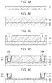
- FIGS. 3 A to 3 H are schematic vertical sectional views illustrating respective steps of manufacturing the semiconductor device 100 according to the present embodiment.
- the insulating layer 330 is deposited on the substrate 310 .
- the insulating layer 330 is formed by depositing Al 2 O 3 or the like by using CVD or the like on the substrate 310 including silicon.
- an oxide film 370 is deposited on the insulating layer 330 .
- the oxide film 370 is formed by depositing SiO x or the like by using CVD or the like on the insulating layer 330 .
- the oxide film 370 may include any material as long as etching selectivity with the insulating layer 330 can be obtained.
- an opening 370 A is formed by removing a part of the oxide film 370 .
- etching is used to remove the oxide film 370 in a region where the source or drain electrode 210 is to be formed at a later stage, whereby the opening 370 A for exposing the insulating layer 330 is formed.
- the source or drain electrode 210 and the barrier layer 230 are formed to fill the opening 370 A.
- the barrier layer 230 is formed by depositing W or the like along a shape of the opening 370 A by using CVD or the like.
- the source or drain electrode 210 is formed by depositing Cu or the like to fill the opening 370 A from above the barrier layer 230 .
- W, Cu, and the like deposited on the oxide film 370 can be removed by using Chemical Mechanical Polishing (CMP), overall etchback, or the like.
- CMP Chemical Mechanical Polishing
- the oxide film 370 is removed. Specifically, the source or drain electrode 210 and the insulating layer 330 are exposed by selectively removing the oxide film 370 by etching or the like.
- the two-dimensional material layer 110 and the gate insulating film 120 are sequentially formed along the outer shapes of the source or drain electrodes 210 and the insulating layer 330 .
- a two-dimensional material such as MoS 2 , and SiO 2 are sequentially deposited by using ALD, CVD, PVD, or the like.
- etching or the like is performed so that MoS 2 and SiO 2 are left that are deposited in a region where a channel is formed from one of the source or drain electrodes 210 to the other of the source or drain electrodes 210 , whereby the two-dimensional material layer 110 and the gate insulating film 120 can be formed.
- the two-dimensional material layer 110 and the gate insulating film 120 can be formed from the side surface of the one of the source or drain electrodes 210 through the surface of the insulating layer 330 to the side surface of the other of the source or drain electrodes 210 .
- the interlayer insulating film 350 is deposited on the insulating layer 330 and the gate insulating film 120 , and a part of the interlayer insulating film 350 is removed to form the opening 350 A.
- the interlayer insulating film 350 is formed by depositing SiO x or the like by using CVD or the like on the insulating layer 330 and the gate insulating film 120 . Thereafter, etching is used to remove the interlayer insulating film 350 in a region where the gate electrode 250 is to be formed at a later stage, whereby the opening 350 A for exposing the gate insulating film 120 is formed.
- the gate electrode 250 and the barrier layer 270 are formed to fill the opening 350 A.
- the barrier layer 270 is formed by depositing W or the like along a shape of the opening 350 A by using CVD or the like.
- the gate electrode 250 is formed by depositing Cu or the like to fill the opening 350 A from above the barrier layer 270 .
- W, Cu, and the like deposited on the interlayer insulating film 350 can be removed by using Chemical Mechanical Polishing (CMP), overall etchback, or the like.
- CMP Chemical Mechanical Polishing
- the semiconductor device 100 according to the present embodiment can be manufactured.
- FIG. 4 is a plan view and a vertical sectional view schematically illustrating the structure of the semiconductor device 101 according to the first modification.
- a source or drain electrode 211 may be provided having a width greater than a width in which the two-dimensional material layer 110 is provided.
- the width (or maximum length) of the source or drain electrode 211 in a direction orthogonal to a direction in which the source or drain electrodes 11 are arranged may be longer than the width of the two-dimensional material layer 110 in the same direction.
- the two-dimensional material layer 110 is provided in a partial region of one side surface of four side surfaces of the source or drain electrode 211 provided in a quadrangular prism shape.
- the semiconductor device 101 according to the first modification it is possible to increase an allowable error of alignment between the source or drain electrode 211 and the two-dimensional material layer 110 .
- the allowable error during the manufacturing of the semiconductor device 101 can be further increased, so that an yield of the semiconductor device 101 can be improved and a manufacturing cost can be reduced.
- FIG. 5 is a plan view and a vertical sectional views schematically illustrating the structure of the semiconductor device 102 according to the second modification.
- a two-dimensional material layer 112 and a gate insulating film 122 may be provided over the entire side surface of the source or drain electrode 210 .
- the two-dimensional material layer 112 and the gate insulating film 122 may be provided on all four side surfaces of the source or drain electrode 210 provided in a quadrangular prism shape.
- each of the source or drain electrodes 210 is provided like an island inside a region where the two-dimensional material layer 112 and the gate insulating film 122 are provided on the surface of the insulating layer 330 .
- a contact area between the source or drain electrode 210 and the two-dimensional material layer 212 can be further increased. That is, in the semiconductor device 102 according to the second modification illustrated in FIG. 5 , in comparison with the semiconductor device 100 illustrated in FIG. 2 , the contact area between the source or drain electrode 210 and the two-dimensional material layer 112 can be increased by about four times. Thus, in the semiconductor device 102 according to the second modification, contact resistance can be further reduced between the source or drain electrode 210 and the two-dimensional material layer 112 .
- FIG. 6 is a vertical sectional view schematically illustrating the structure of the semiconductor device 103 according to the third modification.
- a source or drain electrode 213 may include a lower electrode 223 B and an upper electrode 223 A, and a two-dimensional material layer 113 and a gate insulating film 123 may be provided along outer shapes of the upper electrode 223 A, the lower electrode 223 B, and the insulating layer 330 .
- the source or drain electrode 213 may include the lower electrode 223 B provided on the insulating layer 330 , and the upper electrode 223 A provided on the lower electrode 223 B and having a planar shape smaller than that of the lower electrode 223 B.
- the source or drain electrode 213 is provided in an outer shape having a surface parallel to the surface of the insulating layer 330 .
- the two-dimensional material layer 113 can be provided along the outer shapes of the source or drain electrodes 213 and the insulating layer 330
- the gate insulating film 123 can be provided on the two-dimensional material layer 113 along the outer shapes of the source or drain electrodes 213 and the insulating layer 330 .
- the two-dimensional material layer 113 and the gate insulating film 123 can be continuously provided from a side surface of one of the upper electrodes 223 A through the upper surface of one of the lower electrodes 223 B, the surface of the insulating layer 330 , and the upper surface of the other of the lower electrodes 223 B to a side surface of the other of the upper electrodes 223 A.
- a contact area between the source or drain electrode 213 and the two-dimensional material layer 113 can be further increased. That is, in the semiconductor device 103 according to the third modification illustrated in FIG. 6 , in comparison with the semiconductor device 100 illustrated in FIG. 2 , the contact area between the source or drain electrode 213 and the two-dimensional material layer 113 can be increased by the amount, of the lower electrode 223 B. Thus, in the semiconductor device 103 according to the third modification, contact resistance can be further reduced between the source or drain electrode 213 and the two-dimensional material layer 113 .
- a barrier layer 233 is provided on a surface of the upper electrode 223 A, but the third modification is not limited to such an example.
- the barrier layer 233 may be provided on surfaces of the upper electrode 223 A and the lower electrode 223 B, may be provided only on the surface of the lower electrode 223 B, or may be provided on a surface of the source or drain electrode 213 combining the lower electrode 223 B and the upper electrode 223 A.
- FIG. 7 is a vertical sectional view schematically illustrating the structure of the semiconductor device 104 according to the fourth modification.
- a source or drain electrode 214 may include a lower electrode 224 B and an upper electrode 224 A, and a two-dimensional material layer 114 and a gate insulating film 124 may be provided along outer shapes of the lower electrode 224 B and the insulating layer 330 .
- the source or drain electrode 214 may include the lower electrode 224 B provided on the insulating layer 330 , and the upper electrode 224 A provided on the lower electrode 224 B and having a planar shape smaller than that of the lower electrode 224 B.
- the two-dimensional material layer 114 can be provided along the outer shapes of the lower electrodes 224 B and the insulating layer 330 , and the gate insulating film 124 can be provided on the two-dimensional material layer 114 along the outer shapes of the lower electrodes 224 B and the insulating layer 330 .
- the two-dimensional material layer 114 can be continuously provided from the upper surface of one of the lower electrodes 224 B through the surface of the insulating layer 330 to the upper surface of the other of the lower electrodes 224 B.
- the semiconductor device 104 according to the fourth modification can reduce the difficulty of manufacturing the semiconductor device 104 , so that a manufacturing cost of the semiconductor device 104 can be reduced.
- a barrier layer 234 is provided on a surface of the upper electrode 224 A, but the fourth modification is not limited to such an example.
- the barrier layer 234 may be provided on surfaces of the upper electrode 224 A and the lower electrode 224 B, may be provided only on the surface of the lower electrode 224 B, or may be provided on a surface of the source or drain electrode 214 combining the lower electrode 224 B and the upper electrode 224 A.
- FIG. 8 is a plan view and a vertical sectional view schematically illustrating the structure of the semiconductor device 105 according to the fifth modification.
- a gate electrode 255 may be provided below an insulating layer 335 .
- the gate electrode 255 may be provided being embedded in the substrate 310 below the insulating layer 335 in a region crossing a region where the two-dimensional material layer 110 is formed.
- the gate insulating film 120 is not provided on the two-dimensional material layer 110 , and the insulating layer 335 functions as a gate insulating film.
- the insulating layer 335 may include the inorganic insulating material such as SiO x or SiN x described above as the material of the gate insulating film 120 , or a high dielectric material such as HfO x .
- the semiconductor device 105 according to the fifth modification can reduce a manufacturing cost of the semiconductor device 105 by reducing the difficulty of manufacturing the semiconductor device 105 .
- the gate electrode 255 may include a metal material such as W, Cu, Ti, Al, Pt, or Au, or a metal compound such as TiN or TaN, but the fifth modification is not limited to such an example.
- the gate electrode 255 may be formed by making a conductivity type of impurities introduced into the substrate 310 including a semiconductor such as Si different from that of the surroundings.
- FIG. 9 is a plan view and a vertical sectional view schematically illustrating the structure of the conductive structure according to the present embodiment.
- the conductive structure according to the present embodiment includes the conductive structure 10 described in the first embodiment, and is a conductive structure used in a Back End Of Line (BEOL) for forming a circuit by connecting active elements and the like together by wiring lines.
- BEOL Back End Of Line
- a conductive structure 1000 includes a first wiring layer 216 A, a first interlayer insulating film 366 , a second wiring layer 216 B, a second interlayer insulating film 356 , barrier layers 236 A and 236 B, and a stopper layer 410 , and the two-dimensional material layer 110 .
- the stopper layer 410 , the first wiring layer 216 A, and the two-dimensional material layer 110 form the conductive structure 10 according to the first embodiment.
- the first wiring layer 216 A and the second wiring layer 216 B are respectively provided on surface sides facing each other with respect to the two-dimensional material layer 110 and the stopper layer 410 .
- the first wiring layer 216 A is provided to protrude on the stopper layer 410
- the second wiring layer 216 B is provided on the surface side facing the surface on which the first wiring layer 216 A is provided of the stopper layer 410 .
- the stopper layer 410 is provided with an opening in a region corresponding to a region where the second wiring layer 216 B is provided.
- the two-dimensional material layer 110 is provided from a side surface of the first wiring layer 216 A through one surface of the stopper layer 410 and the opening of the stopper layer 410 to the second wiring layer 216 B.
- the conductive structure 1000 can electrically connect the first wiring layer 216 A and the second wiring layer 216 B to each other. That is, the two-dimensional material layer 110 is provided along outer shapes of the first wiring layer 216 A, the stopper layer 410 , and the second wiring layer 216 B.
- a material forming the first wiring layer 216 A and the second wiring layer 216 B may be similar to that of the source or drain electrode 210 of the semiconductor device 100 according to the second embodiment.
- a material forming the first interlayer insulating film 366 and the second interlayer insulating film 356 may be similar to that of the interlayer insulating film 350 of the semiconductor device 100 according to the second embodiment.
- the barrier layers 236 A and 236 B may be provided on surfaces of the first wiring layer 216 A and the second wiring layer 216 B, respectively, similarly to the barrier layer 230 of the semiconductor device 100 according to the second embodiment.
- the stopper layer 410 includes an insulating material that can ensure etching selectivity with the material forming the first interlayer insulating film 366 and the second interlayer insulating film 356 , and is provided between the first interlayer insulating film 366 and the second interlayer insulating film 356 . As a result, the stopper layer 410 can prevent the etching from progressing penetrating the first interlayer insulating film 366 and the second interlayer insulating film 356 .
- the stopper layer 410 may include SiN x .
- the wiring lines that electrically connect the active elements and the like to each other can include the two-dimensional material layer 110 , so that the wiring lines can be finer and have high conductivity.
- the conductive structure 1000 according to the third embodiment can contribute to downsizing of an integrated circuit (for example, an IC chip) in which a large number of active elements are wired to each other.
- the conductive structure 10 or 1000 , or the semiconductor device 100 according to the embodiment of the present disclosure can be mounted in circuits of various electronic devices.
- FIGS. 10 A to 10 C examples will be described of electronic devices in which the conductive structure 10 or 1000 , or the semiconductor device 100 according to the present embodiment can be mounted.
- FIGS. 10 A to 10 C are external views illustrating examples of electronic devices in which the conductive structure 10 or 1000 , or the semiconductor device 100 according to the present embodiment can be mounted.
- the conductive structure 10 or 1000 , or the semiconductor device 100 according to the present embodiment can be mounted in a circuit of an electronic device such as a smartphone.
- a smartphone 900 includes a display unit 901 that displays various types of information, and an operation unit 903 including buttons and the like that accept an operation input by a user.
- the conductive structure 10 or 1000 , or the semiconductor device 100 according to the present embodiment may be mounted in a control circuit that controls various operations of the smartphone 900 .
- a digital camera 910 includes a main body part (camera body) 911 , an interchangeable lens unit 913 , a grip part 915 gripped by a user at the time of imaging, a monitor unit 917 that displays various types of information, and an Electronic View Finder (EVF) 919 that displays a through image observed by the user at the time of imaging.
- FIG. 10 B is an external view of the digital camera 910 viewed from the front (that is, a subject side), and FIG.
- the conductive structure 10 or 1000 , or the semiconductor device 100 according to the present embodiment may be applied in a control circuit that controls various operations of the digital camera 910 .
- the electronic devices in which the conductive structure 10 or 1000 , or the semiconductor device 100 according to the present embodiment can be mounted are not limited to the examples described above.
- the conductive structure 10 or 1000 , or the semiconductor device 100 according to the present embodiment may be mounted in circuits of electronic devices in any field.
- electronic devices for example, an eyeglass-type wearable device, a Head. Mounted Display (HMD), a television device, an electronic book, a Personal Digital Assistant (PDA), a laptop personal computer, a video camera, a game device, and the like can be exemplified.
- a conductive structure including:
- a metal layer provided on one surface of the insulating layer to protrude in a thickness direction of the insulating layer
- a two-dimensional material layer provided along outer shapes of the metal layer and the insulating layer from a side surface of the metal layer to the one surface of the insulating layer.
- the conductive structure according to (1) in which the two-dimensional material layer has a layered structure in which unit layers each having a two-dimensional structure are laminated.
- a method of for a conductive structure including:
- a semiconductor device including:
- a source electrode and a drain electrode each provided on one surface of the insulating layer to protrude in a thickness direction of the insulating layer;
- a two-dimensional material layer provided along outer shapes of the one surface of the insulating layer, and the source electrode and the drain electrode, from the source electrode to the drain electrode;
- a gate electrode provided in a region overlapping a part of the two-dimensional material layer, with a gate insulating film or the insulating layer sandwiched in a thickness direction of the insulating layer.
- the semiconductor device according to (6) is which the two-dimensional material layer is provided from a side surface of the source electrode to a side surface of the drain electrode.
- the semiconductor device in which the gate electrode is provided in a region crossing a region where the two-dimensional material layer is provided.
- the semiconductor device according to any one of (6) to (8), in which the source electrode and the drain electrode are provided on as identical surface of the insulating layer.
- the semiconductor device according to any one of (6) to (10), in which the two-dimensional material layer is provided over an entire periphery of a side surface of the source electrode or the drain electrode.
- the source electrode or the drain electrode includes a lower electrode provided on the one surface of the insulating layer, and an upper electrode having a planar shape smaller than a planar shape of the lower electrode and provided on the lower electrode, and the two-dimensional material layer is provided at least along an outer shape of the lower electrode.
Landscapes
- Electrodes Of Semiconductors (AREA)
- Engineering & Computer Science (AREA)
- Physics & Mathematics (AREA)
- Condensed Matter Physics & Semiconductors (AREA)
- General Physics & Mathematics (AREA)
- Manufacturing & Machinery (AREA)
- Computer Hardware Design (AREA)
- Microelectronics & Electronic Packaging (AREA)
- Power Engineering (AREA)
- Thin Film Transistor (AREA)
- Chemical & Material Sciences (AREA)
- Crystallography & Structural Chemistry (AREA)
Abstract
Description
- Patent Document 1: Japanese Patent Application Laid-Open No. 2016-219788
-
- 2.1. Structural example
- 2.2. Manufacturing method
- 2.3. Modifications
- 10 Conductive structure
- 11 Two-dimensional material layer
- 21 Metal layer
- 23 Barrier layer
- 31 Substrate
- 33 Insulating layer
- 100, 101, 102, 103, 104, 105 Semiconductor device
- 110, 112, 113, 114 Two-dimensional material layer
- 120, 122, 123, 124 Gate insulating film
- 210, 211, 213, 214 Drain electrode
- 223A, 224A Upper electrode
- 223B, 224B Lower electrode
- 230, 233, 234, 270 Barrier layer
- 250, 255 Gate electrode
- 310 Substrate
- 330, 335 Insulating layer
- 350 Interlayer insulating film
Claims (13)
Applications Claiming Priority (4)
| Application Number | Priority Date | Filing Date | Title |
|---|---|---|---|
| JPJP2018-028251 | 2018-02-20 | ||
| JP2018-028251 | 2018-02-20 | ||
| JP2018028251A JP2021068719A (en) | 2018-02-20 | 2018-02-20 | Conductive structure and formation method therefor, and semiconductor device |
| PCT/JP2019/001904 WO2019163370A1 (en) | 2018-02-20 | 2019-01-22 | Electrically conductive structure, method of forming electrically conductive structure, and semiconductor device |
Publications (2)
| Publication Number | Publication Date |
|---|---|
| US20210005714A1 US20210005714A1 (en) | 2021-01-07 |
| US11563086B2 true US11563086B2 (en) | 2023-01-24 |
Family
ID=67687506
Family Applications (1)
| Application Number | Title | Priority Date | Filing Date |
|---|---|---|---|
| US16/968,670 Active 2039-05-27 US11563086B2 (en) | 2018-02-20 | 2019-01-22 | Conductive structure, method of forming conductive structure, and semiconductor device |
Country Status (7)
| Country | Link |
|---|---|
| US (1) | US11563086B2 (en) |
| JP (1) | JP2021068719A (en) |
| KR (1) | KR102650729B1 (en) |
| CN (1) | CN111712927A (en) |
| DE (1) | DE112019000889T5 (en) |
| TW (1) | TWI833728B (en) |
| WO (1) | WO2019163370A1 (en) |
Families Citing this family (3)
| Publication number | Priority date | Publication date | Assignee | Title |
|---|---|---|---|---|
| KR102138004B1 (en) * | 2018-10-02 | 2020-07-27 | 연세대학교 산학협력단 | Active matrix organic light-emitting diode display device and method of manufacturing the same |
| JP7728603B2 (en) * | 2021-12-22 | 2025-08-25 | 国立研究開発法人産業技術総合研究所 | Electronic/optical device and its manufacturing method |
| CN115566072B (en) * | 2022-10-17 | 2025-09-02 | 瑞砻科技股份有限公司 | Semiconductor element and method for manufacturing the same |
Citations (9)
| Publication number | Priority date | Publication date | Assignee | Title |
|---|---|---|---|---|
| JP2010267752A (en) | 2009-05-14 | 2010-11-25 | Sony Corp | THIN FILM TRANSISTOR, METHOD FOR PRODUCING THIN FILM TRANSISTOR, AND ELECTRONIC DEVICE |
| US20120256167A1 (en) | 2011-04-07 | 2012-10-11 | Samsung Electronics Co., Ltd. | Graphene electronic device and method of fabricating the same |
| WO2014136636A1 (en) | 2013-03-06 | 2014-09-12 | 住友化学株式会社 | Thin film transistor |
| JP2015031666A (en) | 2013-08-06 | 2015-02-16 | 日本電信電話株式会社 | Sensor element |
| JP2015198194A (en) | 2014-04-02 | 2015-11-09 | 株式会社デンソー | semiconductor element |
| JP2017069528A (en) | 2015-10-02 | 2017-04-06 | 日本写真印刷株式会社 | Active device and method for manufacturing active device |
| TW201802948A (en) | 2016-07-01 | 2018-01-16 | 英特爾股份有限公司 | a transistor having a metal source and a drain contact including a Haussler alloy |
| US20180033727A1 (en) * | 2016-07-26 | 2018-02-01 | Taiwan Semiconductor Manufacturing Co., Ltd. | Semiconductor device and manufacturing method thereof |
| US20200395473A1 (en) * | 2018-01-19 | 2020-12-17 | Northwestern University | Self-aligned short-channel electronic devices and fabrication methods of same |
Family Cites Families (10)
| Publication number | Priority date | Publication date | Assignee | Title |
|---|---|---|---|---|
| US8154093B2 (en) | 2002-01-16 | 2012-04-10 | Nanomix, Inc. | Nano-electronic sensors for chemical and biological analytes, including capacitance and bio-membrane devices |
| CN103943599A (en) * | 2013-01-17 | 2014-07-23 | 中国科学院微电子研究所 | Interconnect structure and manufacturing method thereof |
| WO2014162625A1 (en) * | 2013-04-03 | 2014-10-09 | 独立行政法人産業技術総合研究所 | Connection structure, manufacturing method for same, and semiconductor device |
| KR101546500B1 (en) | 2014-09-25 | 2015-08-24 | 성균관대학교산학협력단 | Photodetector and manufacturing method thereof |
| CN104505405A (en) * | 2014-12-30 | 2015-04-08 | 京东方科技集团股份有限公司 | Thin-film transistor and preparing method thereof, array substrate and preparing method thereof, and display device |
| US10217819B2 (en) * | 2015-05-20 | 2019-02-26 | Samsung Electronics Co., Ltd. | Semiconductor device including metal-2 dimensional material-semiconductor contact |
| JP6523197B2 (en) | 2016-03-18 | 2019-05-29 | 東芝メモリ株式会社 | Nonvolatile semiconductor memory device and method of manufacturing the same |
| JP6675945B2 (en) * | 2016-07-19 | 2020-04-08 | 住友電気工業株式会社 | Graphene transistor and method for manufacturing the same |
| CN106601624B (en) * | 2016-12-02 | 2019-04-09 | 厦门市三安集成电路有限公司 | A compound semiconductor metal wiring method and structure |
| CN107425051B (en) * | 2017-07-19 | 2020-10-02 | 苏州能讯高能半导体有限公司 | Semiconductor device and preparation method thereof |
-
2018
- 2018-02-20 JP JP2018028251A patent/JP2021068719A/en active Pending
-
2019
- 2019-01-18 TW TW108101912A patent/TWI833728B/en active
- 2019-01-22 DE DE112019000889.7T patent/DE112019000889T5/en active Pending
- 2019-01-22 KR KR1020207021332A patent/KR102650729B1/en active Active
- 2019-01-22 WO PCT/JP2019/001904 patent/WO2019163370A1/en not_active Ceased
- 2019-01-22 CN CN201980013201.6A patent/CN111712927A/en active Pending
- 2019-01-22 US US16/968,670 patent/US11563086B2/en active Active
Patent Citations (12)
| Publication number | Priority date | Publication date | Assignee | Title |
|---|---|---|---|---|
| JP2010267752A (en) | 2009-05-14 | 2010-11-25 | Sony Corp | THIN FILM TRANSISTOR, METHOD FOR PRODUCING THIN FILM TRANSISTOR, AND ELECTRONIC DEVICE |
| US20120256167A1 (en) | 2011-04-07 | 2012-10-11 | Samsung Electronics Co., Ltd. | Graphene electronic device and method of fabricating the same |
| JP2012222358A (en) | 2011-04-07 | 2012-11-12 | Samsung Electronics Co Ltd | Graphene electronic element and manufacturing method of the same |
| JP6032923B2 (en) | 2011-04-07 | 2016-11-30 | 三星電子株式会社Samsung Electronics Co.,Ltd. | Graphene electronic device and manufacturing method |
| WO2014136636A1 (en) | 2013-03-06 | 2014-09-12 | 住友化学株式会社 | Thin film transistor |
| US20160035903A1 (en) | 2013-03-06 | 2016-02-04 | Osaka University | Thin-film transistor |
| JP2015031666A (en) | 2013-08-06 | 2015-02-16 | 日本電信電話株式会社 | Sensor element |
| JP2015198194A (en) | 2014-04-02 | 2015-11-09 | 株式会社デンソー | semiconductor element |
| JP2017069528A (en) | 2015-10-02 | 2017-04-06 | 日本写真印刷株式会社 | Active device and method for manufacturing active device |
| TW201802948A (en) | 2016-07-01 | 2018-01-16 | 英特爾股份有限公司 | a transistor having a metal source and a drain contact including a Haussler alloy |
| US20180033727A1 (en) * | 2016-07-26 | 2018-02-01 | Taiwan Semiconductor Manufacturing Co., Ltd. | Semiconductor device and manufacturing method thereof |
| US20200395473A1 (en) * | 2018-01-19 | 2020-12-17 | Northwestern University | Self-aligned short-channel electronic devices and fabrication methods of same |
Non-Patent Citations (2)
| Title |
|---|
| International Search Report and Written Opinion prepared by the Japanese Patent Office dated Apr. 11, 2019, for International Application No. PCT/JP2019/001904. |
| Zhang et al, 'Properties of TiN Films Deposited by Atomic Layer Deposition for Through Silicon Via Applications, www.researchgate.net. (Year: 2010). * |
Also Published As
| Publication number | Publication date |
|---|---|
| US20210005714A1 (en) | 2021-01-07 |
| DE112019000889T5 (en) | 2020-10-29 |
| CN111712927A (en) | 2020-09-25 |
| KR102650729B1 (en) | 2024-03-25 |
| WO2019163370A1 (en) | 2019-08-29 |
| TW201935692A (en) | 2019-09-01 |
| TWI833728B (en) | 2024-03-01 |
| KR20200122305A (en) | 2020-10-27 |
| JP2021068719A (en) | 2021-04-30 |
Similar Documents
| Publication | Publication Date | Title |
|---|---|---|
| CN104637438B (en) | Flexible display and its manufacturing method | |
| CN107026190B (en) | display device | |
| TWI844516B (en) | Electrical connection structure, semiconductor device and electronic machine | |
| TW201030966A (en) | Organic light emitting diode display and method of manufacturing the same | |
| US11563086B2 (en) | Conductive structure, method of forming conductive structure, and semiconductor device | |
| CN111293125B (en) | Display device and method for manufacturing the same | |
| CN104620389B (en) | Semiconductor device and its manufacture method | |
| US8124544B2 (en) | Method for manufacturing semiconductor device | |
| TW200934291A (en) | Organic light emitting device and method of fabricating the same | |
| TW201828470A (en) | Semiconductor device | |
| CN113488576A (en) | Light emitting diode structure and manufacturing method thereof | |
| CN112313806A (en) | Display backplane and manufacturing method, display panel and manufacturing method, display device | |
| CN110021632A (en) | Display panel and method for manufacturing the same | |
| EP3032589A2 (en) | Thin film transistor | |
| US20250015243A1 (en) | Display device comprising semiconductor light-emitting element, and manufacturing method therefor | |
| CN111987168A (en) | Thin film transistor, method for manufacturing the same, and display device | |
| KR102521257B1 (en) | Semiconductor device, display panel, and display device including the same | |
| WO2019163324A1 (en) | Protective element and semiconductor device | |
| CN117320480A (en) | Display panel, preparation method and display device thereof | |
| JP7598749B2 (en) | Semiconductor Device | |
| TW201312757A (en) | Thin film transistor structure and manufacturing method thereof | |
| JP6248265B2 (en) | Method for manufacturing thin film transistor substrate | |
| CN119096370A (en) | Thin film transistor, array substrate and display device |
Legal Events
| Date | Code | Title | Description |
|---|---|---|---|
| FEPP | Fee payment procedure |
Free format text: ENTITY STATUS SET TO UNDISCOUNTED (ORIGINAL EVENT CODE: BIG.); ENTITY STATUS OF PATENT OWNER: LARGE ENTITY |
|
| STPP | Information on status: patent application and granting procedure in general |
Free format text: APPLICATION DISPATCHED FROM PREEXAM, NOT YET DOCKETED |
|
| AS | Assignment |
Owner name: SONY SEMICONDUCTOR SOLUTIONS CORPORATION, JAPAN Free format text: ASSIGNMENT OF ASSIGNORS INTEREST;ASSIGNOR:TOMIDA, KAZUYUKI;REEL/FRAME:055692/0665 Effective date: 20210303 |
|
| STPP | Information on status: patent application and granting procedure in general |
Free format text: DOCKETED NEW CASE - READY FOR EXAMINATION |
|
| STPP | Information on status: patent application and granting procedure in general |
Free format text: NON FINAL ACTION MAILED |
|
| STPP | Information on status: patent application and granting procedure in general |
Free format text: FINAL REJECTION MAILED |
|
| STPP | Information on status: patent application and granting procedure in general |
Free format text: RESPONSE AFTER FINAL ACTION FORWARDED TO EXAMINER |
|
| STPP | Information on status: patent application and granting procedure in general |
Free format text: ADVISORY ACTION MAILED |
|
| STPP | Information on status: patent application and granting procedure in general |
Free format text: DOCKETED NEW CASE - READY FOR EXAMINATION |
|
| STPP | Information on status: patent application and granting procedure in general |
Free format text: NOTICE OF ALLOWANCE MAILED -- APPLICATION RECEIVED IN OFFICE OF PUBLICATIONS |
|
| STPP | Information on status: patent application and granting procedure in general |
Free format text: PUBLICATIONS -- ISSUE FEE PAYMENT VERIFIED |
|
| STCF | Information on status: patent grant |
Free format text: PATENTED CASE |