US11549056B2 - Compositions and methods relating to luminescent structures - Google Patents
Compositions and methods relating to luminescent structures Download PDFInfo
- Publication number
- US11549056B2 US11549056B2 US16/323,824 US201716323824A US11549056B2 US 11549056 B2 US11549056 B2 US 11549056B2 US 201716323824 A US201716323824 A US 201716323824A US 11549056 B2 US11549056 B2 US 11549056B2
- Authority
- US
- United States
- Prior art keywords
- precipitate
- pbbr
- zero
- dimensional perovskite
- perovskite
- Prior art date
- Legal status (The legal status is an assumption and is not a legal conclusion. Google has not performed a legal analysis and makes no representation as to the accuracy of the status listed.)
- Active, expires
Links
Images


Classifications
-
- C—CHEMISTRY; METALLURGY
- C09—DYES; PAINTS; POLISHES; NATURAL RESINS; ADHESIVES; COMPOSITIONS NOT OTHERWISE PROVIDED FOR; APPLICATIONS OF MATERIALS NOT OTHERWISE PROVIDED FOR
- C09K—MATERIALS FOR MISCELLANEOUS APPLICATIONS, NOT PROVIDED FOR ELSEWHERE
- C09K11/00—Luminescent materials, e.g. electroluminescent or chemiluminescent
- C09K11/08—Luminescent materials, e.g. electroluminescent or chemiluminescent containing inorganic luminescent materials
- C09K11/66—Luminescent materials, e.g. electroluminescent or chemiluminescent containing inorganic luminescent materials containing germanium, tin or lead
- C09K11/664—Halogenides
- C09K11/665—Halogenides with alkali or alkaline earth metals
-
- C—CHEMISTRY; METALLURGY
- C01—INORGANIC CHEMISTRY
- C01G—COMPOUNDS CONTAINING METALS NOT COVERED BY SUBCLASSES C01D OR C01F
- C01G21/00—Compounds of lead
- C01G21/006—Compounds containing lead, with or without oxygen or hydrogen, and containing two or more other elements
-
- C—CHEMISTRY; METALLURGY
- C09—DYES; PAINTS; POLISHES; NATURAL RESINS; ADHESIVES; COMPOSITIONS NOT OTHERWISE PROVIDED FOR; APPLICATIONS OF MATERIALS NOT OTHERWISE PROVIDED FOR
- C09K—MATERIALS FOR MISCELLANEOUS APPLICATIONS, NOT PROVIDED FOR ELSEWHERE
- C09K11/00—Luminescent materials, e.g. electroluminescent or chemiluminescent
- C09K11/08—Luminescent materials, e.g. electroluminescent or chemiluminescent containing inorganic luminescent materials
- C09K11/0827—Halogenides
- C09K11/0833—Halogenides with alkali or alkaline earth metals
-
- C—CHEMISTRY; METALLURGY
- C01—INORGANIC CHEMISTRY
- C01P—INDEXING SCHEME RELATING TO STRUCTURAL AND PHYSICAL ASPECTS OF SOLID INORGANIC COMPOUNDS
- C01P2002/00—Crystal-structural characteristics
- C01P2002/30—Three-dimensional structures
- C01P2002/34—Three-dimensional structures perovskite-type (ABO3)
-
- C—CHEMISTRY; METALLURGY
- C01—INORGANIC CHEMISTRY
- C01P—INDEXING SCHEME RELATING TO STRUCTURAL AND PHYSICAL ASPECTS OF SOLID INORGANIC COMPOUNDS
- C01P2006/00—Physical properties of inorganic compounds
- C01P2006/80—Compositional purity
Definitions
- the present disclosure generally relates to luminescent structures and related methods for their synthesis and/or separation.
- Zero-dimensional perovskites such as Cs 4 PbBr 6 , promise outstanding emissive properties.
- current synthetic methods for such highly emissive materials are mostly based on the melting of precursor materials (such as CsBr and PbBr 2 ). Melting of precursor products usually can lead to the co-formation of undesired phases and impure products, due to incongruent melting of reaction products, such as Cs 4 PbBr 6 . Utilization of impure products is not desired as the impure products may not meet the potential physical properties of pure products, preventing the widespread adoption of highly emissive and/or luminescent structures, such as those with zero-dimensional perovskites.
- Embodiments of the present disclosure describe a method for synthesizing a zero-dimensional perovskite comprising mixing at least one of CsR or Cs(R) 2 with at least one of PbR or Pb(R) 2 in a solvent to create a mixture, wherein R is at least one of a halogen, a halogen anion, a monovalent anion, or the conjugate base of an acid; heating the mixture to a temperature in a range of about 40° C. to about 180° C.
- a method for synthesizing a zero-dimensional perovskite comprises: mixing at least one of CsR or Cs(R) 2 with at least one of PbR or Pb(R) 2 in a solvent to create a mixture, wherein R is at least one of a halogen, a halogen anion, a monovalent anion, or the conjugate base of an acid; heating the mixture to a temperature in a range of about 40° C. to about 180° C.
- a method for synthesizing a zero-dimensional perovskite comprises: mixing at least one of CsR or Cs(R) 2 with at least one of PbR or Pb(R) 2 in a solvent to create a mixture, wherein R is at least one of a halogen, a halogen anion, a monovalent anion, or the conjugate base of an acid; mixing the mixture with an antisolvent vapor and exposing the mixture to the antisolvent vapor for a period of time to form a precipitate; isolating the precipitate; washing the precipitate with a wash solvent to produce a washed precipitate; and drying the washed precipitate by a drying method to produce a zero-dimensional perovskite.
- a zero-dimensional perovskite composition comprising at least 95% pure solid zero-dimensional perovskite, wherein the zero-dimensional perovskite has a formula of Cs 4 Pb(R 1 ) 6 , wherein R 1 is a halogen, a halogen anion, or the conjugate base of an acid, and a photoluminescence quantum yield of about 38% or greater.
- FIG. 1 shows photos perovskites excitations under ultraviolet (UV) light, according to one or more embodiments of the present disclosure.
- UV ultraviolet
- FIG. 2 ( a ) depicts a crystal structure of CsPbBr 3 , according to one or more embodiments of the present disclosure.
- FIG. 2 ( b ) depicts Cs 4 PbBr 6 featuring corner-shared and PbBr 6 octahedra, according to one or more embodiments of the present disclosure.
- FIG. 3 ( a ) is schematic representation of the optimization of a method for the synthesis and separation of a perovskite (percentages represent the ratios of x-ray diffraction or XRD peak intensities), according to one or more embodiments of the present disclosure.
- FIG. 3 ( b ) depicts powder x-ray diffraction (PXRD) patterns of synthesized solid Cs 4 PbBr 6 along with the calculated spectrum of the same, according to one or more embodiments of the present disclosure.
- PXRD powder x-ray diffraction
- FIG. 4 ( a ) shows ground CsPbBr 3 on a slide under ambient (left) and UV (right, 365 nm) light, according to one or more embodiments of the present disclosure.
- FIG. 4 ( b ) illustrates Cs 4 PbBr 6 powder on a glass slide under ambient (left) and UV (right, 365 nm) light, according to one or more embodiments of the present disclosure.
- FIG. 4 ( c ) depicts the absorption spectra of solid Cs 4 PbBr 6 excited at 365 nm wavelength, according to one or more embodiments of the present disclosure.
- FIG. 4 ( d ) shows photoluminescent (PL) spectra of Cs 4 PbBr 6 excited at 365 nm wavelength, according to one or more embodiments of the present disclosure.
- FIG. 5 ( a ) depicts the complete spectra of Cs 4 PbBr 6 for photoluminescent quantum yield (PLQY) measurement using integrating sphere, according to one or more embodiments of the present disclosure.
- the PL spectra were enlarged by a factor of 15 for clarity.
- FIG. 5 ( b ) shows temperature-dependent PL spectra from 77 K to 360 K, according to one or more embodiments of the present disclosure.
- FIG. 5 ( c ) shows PL lifetime decay of Cs 4 PbBr 6 , according to one or more embodiments of the present disclosure.
- FIG. 6 ( a ) depicts the evaluation of PL spectra with increasing optical pump fluence for solid Cs 4 PbBr 6 powders, according to one or more embodiments of the present disclosure.
- FIG. 6 ( b ) shows PL intensity as a function of pump fluence for solid Cs 4 PbBr 6 powders, according to one or more embodiments of the present disclosure. Transition from spontaneous emission (SE) to amplified spontaneous emission (ASE) with the threshold value of 68 ⁇ J/cm 2 .
- SE spontaneous emission
- ASE amplified spontaneous emission
- FIG. 7 illustrates rapid precipitation from a reaction of CsBr/PbBr 2 (1/1) solution in dimethylsulfoxide (DMSO) with DCM, according to one or more embodiments of the present disclosure.
- X-ray diffraction shows that the resultant powder can be the mixture of CsPbBr 3 and CsPb 2 Br 5 .
- FIG. 8 depicts filtered solutions, products resulting from reactions of CsBr/PbBr 2 (1/1, leftmost in figure), (1.25/1, middle in figure), and (1.5/1, rightmost in figure) in DMSO after 3 hours at 120° C., according to one or more embodiments of the present disclosure.
- FIG. 9 shows undissolved powder from a reaction of CsBr/PbBr 2 (1.5/1) in DMSO, according to one or more embodiments of the present disclosure.
- XRD data shows it can consist mainly of CsBr, CsPbBr 3 , and Cs 4 PbBr 6 .
- FIG. 10 is an example demonstration of good solubility of CsPbBr 3 and poor solubility of Cs 4 PbBr 6 in DMSO, according to one or more embodiments of the present disclosure.
- FIG. 11 shows an example analysis of temperature-dependent PL of a perovskite powder, according to one or more embodiments of the present disclosure.
- FIG. 12 ( a ) shows a schematic representation of the Cs 4 PbBr 6 single crystal synthesis by the solvent vapor method, according to one or more embodiments of the present disclosure.
- FIG. 12 ( b ) shows fluorescent (top) and optical microscope picture of the single crystals (bottom) (scale bar: 500 ⁇ m), according to one or more embodiments of the present disclosure.
- FIG. 12 ( c ) shows SEM image of the single crystal (scale bar: 50 ⁇ m), according to one or more embodiments of the present disclosure.
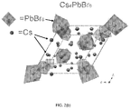
- FIG. 12 ( d ) shows crystal structure of Cs 4 PbBr 6 obtained from SC-XRD, with octahedral representing the isolated PbBr 6 characteristic of 0D perovskite, according to one or more embodiments of the present disclosure.
- FIG. 12 ( e ) shows XRD patterns of ground Cs 4 PbBr 6 (bottom) and calculated single crystal of Cs 4 PbBr 6 (top), according to one or more embodiments of the present disclosure.
- Embodiments of the present disclosure will employ, unless otherwise indicated, techniques of sample preparation, analytical chemistry, chemical analysis, chemical synthesis, and the like, which are within the skill of the art. Such techniques are explained fully in the literature.
- compositions and methods relating to luminescent structures are not limited to particular types of compositions and methods relating to luminescent structures, particular subjects (e.g. human, animal, plant or inanimate), and particular software[s] for post-processing and analysis, or the like, as such can vary.
- terminology used herein is for purposes of describing particular embodiments only, and is not intended to be limiting. It is also possible in the present disclosure that steps can be executed in different sequence where this is logically possible.
- the present disclosure is directed to compositions and methods relating to luminescent structures (e.g., pure luminescent structures).
- the present disclosure relates to pure luminescent structures with remarkable emission properties and new solution-processed methods for the synthesis and separation of the pure luminescent structures.
- the photoluminescence quantum yield (PLQY) of the luminescent structures for example Cs 4 PbBr 6
- CsPbBr 3 in solid form surprisingly can reach 38% or more, while its three-dimensional counterpart—CsPbBr 3 —exhibits almost two-half orders of magnitude lower PLQY.
- this dramatic increase in photoluminescence can be due to defects in the unique crystal structure of the product, adopting the Bergerhoff-Schmitz-Dumont crystal type, in which metal-halide octahedral are spatially confined.
- a luminescent structure can be a luminescent perovskite.
- a luminescent structure can be a zero-dimensional (0D) perovskite.
- a luminescent structure can be a zero-dimensional (0D) luminescent perovskite.
- the luminescent structures can be pure.
- the luminescent structures can be one or more of pure luminescent perovskite and pure zero-dimensional (0D) luminescent perovskite.
- pure is meant to mean a purity of 95% or greater.
- the luminescent structures of the present disclosure, such as zero-dimensional (0D) luminescent perovskite can be used, for example, as photodetectors, light emitters (including LEDs), and light converters, among other things.
- a luminescent structure or 0D perovskite as described herein can be luminescent and have the formula Cs 4 Pb(R 1 ) 6 , wherein R 1 can be an anion, a halogen, a conjugate base of an acid, or others.
- R 1 is a halogen.
- R 1 is a halogen anion.
- the halogen is CI, Br or I.
- R 1 is CH 3 COO ⁇ .
- a luminescent structure can be purified Cs 4 PbBr 6 .
- a luminescent structure can be solid or solid purified Cs 4 PbCl 6 , Cs 4 PbI 6 , Cs 4 Pb(CH 3 COO) 6 , or other compounds.
- Purified structures, compositions, or perovskites as described herein can have a purity of about 95% or greater.
- a luminescent structure can be a photodetector. In an embodiment, a luminescent structure can be a photodetector and can be a luminescent perovskite. In an embodiment, a luminescent structure can be a photodetector and can be a 0D luminescent perovskite. In an embodiment, a luminescent structure can be a photodetector and can be Cs 4 PbBr 6 , Cs 4 PbCl 6 , Cs 4 PbI 6 , or Cs 4 Pb(CH 3 COO) 6 . In an embodiment, a luminescent structure can be an emitting 0D luminescent perovskite that can be used for example for color converters, light-emitting diodes, lasers, and other opto-electronic applications.
- R can be a monovalent anion, a halogen, a halogen anion, a conjugate base of an acid, or others.
- R is a halogen.
- R is a halogen anion.
- R is Br, CI, I, or CH 3 COO.
- R is Br ⁇ , Cl ⁇ , I ⁇ , or CH 3 COO ⁇ .
- starting materials such as CsBr and PbBr 2
- a solvent such as dimethyl sulfoxide (DMSO).
- DMSO dimethyl sulfoxide
- other starting materials for the method described herein can be used, such as CsCl, CsI, PbCl 2 , PbI 2 , CsBr, Cs(CH 3 COO), Pb(CH 3 COO) 2 , CsBr 2 , PbBr 2 , HBr, CsBr 2 —PbBr 2 —HBr, among others.
- Other solvents can be used, such as DMSO-DMF, DMF, and GBL, among others.
- the starting materials can be mixed in a ratio of 0.1:1 to 1:0.1, optionally in a 1:1 ratio. In an embodiment, mixing can be done with a ratio of about 1 to about 1. In an embodiment, 1 mL of DMSO can be used for every 1 mmol of CsBr and 1 mmol of PbBr 2 .
- a precipitate may be formed by heating the mixture.
- the mixture can be heated to a desired final temperature of about 40° C. to about 180° C., for example, to about 120° C. over a first period of time, for example, about 10 to about 300 minutes.
- the mixture can be held at a temperature of about 40° C. to about 180° C., for example, at about 120° C., and incubated at the desired final temperature for a second period of time, for example, about 10 minutes to about 300 minutes, optimally for about an hour, to allow the mixture to continue to react and complete its reaction.
- the mixture can optionally be stirred during heating to improve reaction efficacy. This reaction can form a precipitate.
- the precipitate can be a powder or single crystal.
- the precipitate can be a perovskite powder or single crystal.
- the precipitate can be formed by mixing the mixture with an antisolvent vapor and exposing the mixture to the antisolvent vapor for a period of time to form a precipitate.
- the antisolvent vapor includes a solvent vapor in which the 0D perovskite is non-soluble, leading to decreasing solubility of 0D in entire mixture and formation of its precipitate.
- the antisolvent vapor may include one or more of hydrocarbons, halocarbons, ethers, and ketones.
- the hydrocarbons may include, but are not limited to, hexane, toluene, and benzene; the halocarbons may include, but are not limited to, chloroform; the ethers may include, but are not limited to, dimethyl ether and diethyl ether; and the ketones may include, but are not limited to, acetone.
- the mixture can be exposed to the antisolvent vapor for a period of time to form a precipitate. The period of time can be about one hour or more.
- the precipitate can be a powder or single crystal. In an embodiment, the precipitate can be a perovskite powder or single crystal.
- the precipitate formed by the reaction can be isolated, filtered, or otherwise separated from the solvent and other impurities or undesired reaction by-products.
- a precipitate formed can be isolated by filtering with a filter apparatus, for example, after heating and incubation.
- a filtering apparatus as described herein can be standard laboratory filter paper or Whatman® filter paper that separates the precipitate product from the solvent.
- the precipitation can be collected with by Buchner bulb. Also, it may be isolated by sedimenting by a centrifugation method, such as ultracentrifugation, and separated from liquid through a method such as decanting the liquid.
- the precipitate can be dried at room temperature (e.g., by storing the precipitate at room temperature) or heated over a period of time to a temperature in the range of 40 to 180 QC, for example, to about 120° C., and can be held or incubated at said temperature for a period of time, for example, 0.5 to 50 hours, preferably for about three hours.
- the precipitate can be washed with a volume of a wash solvent, such as DMSO, to create a washed precipitate or washed reaction product.
- a wash solvent such as DMSO
- Other solvents such as DMSO-DMF, DMF, GBL, and others can be used in place of DMSO. It can be desirable that the precipitate formed by the reaction not be soluble in the wash solvent.
- a purified reaction product which can be a luminescent structure or luminescent perovskite and can be a powder, remains as a precipitate and impurities can be dissolved into and washed away with the solvent.
- a precipitate can be isolated again from the solvent, and can be isolated with a filtering apparatus.
- the washed participate can be dried by a drying method to produce a luminescent structure (e.g., a washed and/or dried precipitate).
- the washed precipitate can be dried and residual solvent removed by storing at room temperature or heating to an elevated temperature, such as about 100° C., and incubating or holding the washed precipitate at the elevated temperature for a period of time, for example 6 to 16 hours. As an example the washed precipitate can be incubated overnight.
- a washed and dried reaction precipitate product can be a powder or single crystal. A washed and dried precipitate can have a purity of about 95% or greater. A washed and dried reaction product can be a luminescent structure. A washed and dried reaction product can be a luminescent perovskite. A washed and dried reaction precipitate product can be a zero-dimensional (0D) luminescent perovskite. A washed and dried reaction precipitate product can be a zero-dimensional luminescent perovskite and have a purity of at least about 95%. A washed and dried reaction precipitate product can be a purified Cs 4 PbBr 6 composition that can be at least 95% pure, up to 100% pure solid Cs 4 PbBr 6 .
- a washed and dried precipitate can be a purified Cs 4 PbBr 6 composition with a photoluminescence quantum yield (PLQY) of at least about 38% (e.g., about 38% to about 40%) and an emission peak at 515-525 nm following excitation at 365 nm.
- a purified Cs 4 PbBr 6 composition can be a powder.
- a washed and dried reaction precipitate product can be Cs 4 PbCl 6 , Cs 4 PbI 6 , Cs 4 Pb(CH 3 COO) 6 , or others.
- Embodiments of the present disclosure further describe a zero-dimensional perovskite composition, comprising at least 95% pure solid zero-dimensional perovskite, wherein the zero-dimensional perovskite has a formula of Cs 4 Pb(R 1 ) 6 wherein R 1 is a halogen, a halogen anion, or the conjugate base of an acid and a photoluminescence quantum yield of about 38% or greater.
- the zero-dimensional composition can be at least one of purified Cs 4 PbBr 6 , Cs 4 PbCl 6 , Cs 4 PbI 6 , or Cs 4 Pb(CH 3 COO) 6 .
- the zero-dimensional perovskite composition can be a purified Cs 4 PbBr 6 composition, comprising at least 95% pure solid Cs 4 PbBr 6 with a photoluminescence quantum yield of at least about 38% and an emission peak at about 515-525 nm following excitation at 365 nm.
- the Cs 4 PbBr 6 composition can be a powder or single crystal and can have a purity of about 95% to about 100%.
- the Cs 4 PbBr 6 composition can have a purity of about 100%.
- a purified Cs 4 PbBr 6 composition can be a 95% or greater pure solid powder Cs 4 PbBr 6 .
- the Cs 4 PbBr 6 composition can have a photoluminescence quantum yield (PLQY) of at least about 38% and an emission peak at about 515-525 nm following excitation at 365 nm.
- PLQY photoluminescence quantum yield
- PLQY's of the perovskite compositions described herein can be at least about 38% or greater, at least about 35% or greater, at least about 30% or greater, at least about 25% or greater, at least about 20% of greater, at least about 15% or greater, or at least 15% or greater.
- an emission peak is not intended to encompass only one wavelength. Emission peaks can encompass one or more wavelengths at one or more intensity, they can be sharp or broad, and can vary depending on the specific composition.
- Photoluminescence quantum yield (PLQY) of semiconductor materials define their trap state densities and applicability for optoelectronic applications like solar cells, color converters, lasers, light-emitting diodes, and others.
- An ideal emitter can exhibit near-unity PLQY due to absence of trap states within its band gap.
- Recent reports on perovskite single crystals have estimated an ultralow trap state densities—in the order of ⁇ 10 10 cm ⁇ 3 . Yet, those bulk perovskites are not optically emissive, most likely due to the shared octahedra of the crystal structure that prevents quantum confinement of the charge carriers.
- the excitons have extremely low binding energies ( ⁇ 15-50 meV which is in the order of thermal energy) and dissociate to free carriers.
- Quantum confinement and consequent high PLQY are realized in perovskite quantum dots due to the nanoscale physical sizes stabilized by ligands, and in perovskite thin films due to the nanoscale grain sizes.
- the PLQY of quantum dots remarkably decreases when they are made into solid form, because of loss of capping ligands causing further aggregation.
- the abundance of grain boundaries are detrimental to their stability.
- perovskites An alternative approach to achieve quantum confinement can be to reduce the dimensionality of perovskites.
- the general formula of perovskites can be written as AnBX 2+n , where A is a monovalent cation like CH 3 NH 3+ , Cs + , etc., B is a divalent metal, usually Pb 2+ or Sn 2+ , and X is a halogen anion.
- CsPbBr 3 is a 3D perovskite, the crystal structure of which is based on the corner-shared PbBr 6 octahedra ( FIG. 1 , FIG. 2 ( a ) ).
- FIG. 3 ( a ) summarizes some of the explored parameters used to optimize Cs 4 PbBr 6 synthesis to arrive to pure Cs 4 PbBr 6 .
- Rapid precipitation from CsBr/PbBr 2 (1/1) in dimethyl sulfoxide (DMSO) solution was used as a starting point.
- An antisolvent (dichloromethane, DCM) was then added.
- this reaction scheme resulted in a mixture of undesired phases—CsPbBr 3 and CsPb 2 Br 5 ( FIG. 7 ).
- FIG. 5 ( a ) To quantify the PL, the PLQY of these solids ( FIG. 5 ( a ) ) was measured following the method reported by de Mellon et. al. While measurement of the PLQY of 3D perovskite was not possible because of low luminescence (PLQY ⁇ 0.1%), that of 0D perovskite was found to be remarkably high ( ⁇ 38%). Alternatively, from temperature dependent PL measurements ( FIG. 5 ( b ) ), an estimated ⁇ 40% PLQY at room temperature ( FIG. 11 ) was obtained, which is in a good agreement with the previous measurement. This increased difference in PLQY in 0D and 3D perovskites can originate from their unique structures.
- a method for isolation of a Cs 4 PbBr 6 monophasic solid is provided herein, and its emission properties studied.
- the isolated Cs 4 PbBr 6 demonstrates a high PLQY compared to its 3D perovskite counterparts. These results represent a better understanding of the Cs—Pb—Br perovskite family.
- Previous reports on Cs 4 PbBr 6 solids show the coexistence of both 0D and 3D phases, which limited applications that rely on one of the compounds. Further, the use of solids for ASE was demonstrated, that showing the isolated solids can be good color converters, light-emitting diodes (LED), and other optoelectronic applications.
- the crystals are collected and washed with IPA/DMSO (3:1 v:v) mixed solvent (to remove the leftover solution) then dried and stored in a nitrogen atmosphere.
- the size of the crystals varies according to the crystallization time (i.e. more time spent for crystallization results in larger crystals): here, 500- ⁇ m crystals after 48 hours of crystallization were collected.
- the crystals exhibited a pale green color under ambient light, but when exposed to 365 nm UV irradiation, they luminesced bright green light ( FIG. 12 ( b ) ).
- Scanning Electron Microscopy (SEM) images confirmed the high quality of the crystals with smooth surfaces and well-defined rhomboid shape ( FIG. 12 ( c ) ).
- SC-XRD single crystal X-Ray Diffraction
- the PL profile of Cs 4 PbBr 6 exhibited a standard Gaussian peak centered at 524 nm with a FWHM of 24 nm. The PL peak partially overlapped with the absorption edge with a small Stokes shift of ⁇ 28 meV.
- the PLQY values of Cs 4 PbBr 6 single crystals were measured with an integrating sphere under an excitation wavelength of 420 nm. PLQY values between 40-42% were obtained from different crystals of differed sizes. It is understood that these PLQY values are the highest reported to date for single crystals of halide perovskites.
- the powder X-ray diffraction (PXRD) was performed on a Bruker AXS D8 diffractometer using Cu-K ⁇ radiation.
- the steady-state absorption was recorded using a Cary 6000i UV-Vis-NIR Spectrophotometer with integrated sphere in diffuse-reflectance mode.
- the photoluminescence spectra were characterized using a Horiba JY LabRAM Aramis spectrometer with an Olympus 50 ⁇ lens in a Linkam THMS600 stage. A 473 nm laser was used as the excitation source.
- FIG. 7 shows rapid precipitation from CsBr/PbBr 2 ( 1 / 1 ) solution in DMSO with DCM.
- XRD shows that the resultant powder can be a mixture of CsPbBr 3 and CsPb 2 Br 5 .
- FIG. 8 demonstrates filtered solutions of CsBr/PbBr 2 (1/1), (1.25/1) and (1.5/1) in DMSO after keeping at 120° C. for 3 h.
- FIG. 9 depicts undissolved powder from CsBr/PbBr 2 (1.5/1) in DMSO. It can consist of mainly CsBr, CsPbBr 3 and Cs 4 PbBr 6 . CsBr does not dissolve completely, and when precipitated, can partially react with PbBr 2 . This can result in decreasing PbBr 2 concentration. Therefore, the inverse solubility from this solution may not be observed.
- FIG. 10 is an example demonstration of suitable solubility of CsPbBr 3 and unsuitable solubility of Cs 4 PbBr 6 in DMSO. This observation allows for the clean separation of Cs 4 PbBr 6 from CsPbBr 3 .
- FIG. 11 is an analysis of temperature-dependent PL.
- the integrated PL peak at 300 K is 20 k.
- FWHM decreases by decreasing the temperature, reaching 10 nm at 77K.
- Exciton binding energy can be estimated using the following fitting.
- I T I O 1 + A ⁇ ⁇ exp ⁇ ( - E B k B ⁇ T )
- I T is the integrated intensity at T K
- E B is the binding energy
- k B is the Boltzmann constant
- Ratios, concentrations, amounts, and other numerical data may be expressed in a range format. It is to be understood that such a range format is used for convenience and brevity, and should be interpreted in a flexible manner to include not only the numerical values explicitly recited as the limits of the range, but also to include all the individual numerical values or sub-ranges encompassed within that range as if each numerical value and sub-range is explicitly recited.
- a concentration range of “about 0.1% to about 5%” should be interpreted to include not only the explicitly recited concentration of about 0.1% to about 5%, but also include individual concentrations (e.g., 1%, 2%, 3%, and 4%) and the sub-ranges (e.g., 0.5%, 1.1%, 2.2%, 3.3%, and 4.4%) within the indicated range.
- the term “about” can include traditional rounding according to significant figure of the numerical value.
- the phrase “about ‘x’ to ‘y’” includes “about ‘x’ to about ‘y’”.
Landscapes
- Chemical & Material Sciences (AREA)
- Organic Chemistry (AREA)
- Inorganic Chemistry (AREA)
- Engineering & Computer Science (AREA)
- Materials Engineering (AREA)
- Luminescent Compositions (AREA)
Abstract
Description
where IT is the integrated intensity at T K, EB is the binding energy, and kB is the Boltzmann constant.
Claims (17)
Priority Applications (1)
| Application Number | Priority Date | Filing Date | Title |
|---|---|---|---|
| US16/323,824 US11549056B2 (en) | 2016-08-26 | 2017-08-25 | Compositions and methods relating to luminescent structures |
Applications Claiming Priority (3)
| Application Number | Priority Date | Filing Date | Title |
|---|---|---|---|
| US201662380131P | 2016-08-26 | 2016-08-26 | |
| US16/323,824 US11549056B2 (en) | 2016-08-26 | 2017-08-25 | Compositions and methods relating to luminescent structures |
| PCT/IB2017/055135 WO2018037387A1 (en) | 2016-08-26 | 2017-08-25 | Compositions and methods relating to luminescent structures |
Publications (2)
| Publication Number | Publication Date |
|---|---|
| US20190169498A1 US20190169498A1 (en) | 2019-06-06 |
| US11549056B2 true US11549056B2 (en) | 2023-01-10 |
Family
ID=60043247
Family Applications (1)
| Application Number | Title | Priority Date | Filing Date |
|---|---|---|---|
| US16/323,824 Active 2037-12-19 US11549056B2 (en) | 2016-08-26 | 2017-08-25 | Compositions and methods relating to luminescent structures |
Country Status (2)
| Country | Link |
|---|---|
| US (1) | US11549056B2 (en) |
| WO (1) | WO2018037387A1 (en) |
Families Citing this family (21)
| Publication number | Priority date | Publication date | Assignee | Title |
|---|---|---|---|---|
| CN108511564A (en) * | 2018-02-28 | 2018-09-07 | 湖北大学 | One kind being based on GaN/CsPbBr3Photoresponse type LED of hetero-junctions and preparation method thereof |
| CN108483487B (en) * | 2018-04-26 | 2019-12-13 | 吉林大学 | A preparation method of Cs4PbBr6 perovskite nanocrystals with controllable size and shape |
| CN108832001B (en) * | 2018-06-21 | 2022-04-15 | 南京邮电大学 | Lead-free perovskite solar cell device and preparation method thereof |
| CN109103274B (en) * | 2018-07-28 | 2020-03-31 | 陕西师范大学 | A kind of all-inorganic perovskite solar cell and preparation method thereof |
| CN111500288B (en) * | 2019-01-31 | 2023-06-02 | 隆达电子股份有限公司 | Manufacturing method of perovskite nano light-emitting crystal |
| CN109777416A (en) * | 2019-03-25 | 2019-05-21 | 重庆大学 | A kind of zero dimension perovskite caesium lead bromine nanometer sheet and its preparation method and application |
| CN110515113A (en) * | 2019-08-02 | 2019-11-29 | 南京理工大学 | Core-shell structure halogen perovskite X-ray scintillator and preparation method thereof |
| CN110776000B (en) * | 2019-09-18 | 2021-12-10 | 广东工业大学 | All-inorganic perovskite nanocrystalline, preparation method thereof and application thereof in semiconductor device |
| CN110606505B (en) * | 2019-10-21 | 2022-03-25 | 江苏科技大学 | Zero-dimensional halogen perovskite structure material Cs4PbBr6Preparation and use of |
| CN111477746B (en) * | 2020-04-24 | 2022-03-04 | 武汉大学 | Low-temperature doped high photoluminescence quantum yield perovskite thin film and preparation method thereof |
| CN111960461A (en) * | 2020-07-20 | 2020-11-20 | 齐鲁工业大学 | Zero-dimensional perovskite Cs capable of regulating and controlling laser performance4PbBr6Micron crystal and preparation method thereof |
| CN112064115A (en) * | 2020-08-11 | 2020-12-11 | 南京航空航天大学 | Cs (volatile organic Compounds)4PbI6Perovskite crystal, preparation method and application |
| CN111944525B (en) * | 2020-08-25 | 2022-05-10 | 深圳大学 | Zero-dimensional cesium lead bromine inorganic perovskite material and preparation method thereof |
| KR102805793B1 (en) * | 2020-09-28 | 2025-05-14 | 삼성전자주식회사 | Method for manufacturing light-emitting material, light-emitting manufactured thereby and light-emitting device comprising same |
| CN112876084B (en) * | 2020-12-25 | 2022-12-09 | 温州大学 | Quantum dot glass ceramics and preparation method thereof and method for preparing quantum dot glass ceramics product by applying 3D printing technology |
| US12490576B2 (en) * | 2021-11-26 | 2025-12-02 | Board Of Regents, The University Of Texas System | 3D-0D perovskite light-emitting electrochemical cells |
| CN114645327B (en) * | 2022-02-11 | 2023-11-07 | 上海大学 | Perovskite single crystal and growth method thereof |
| CN114560495A (en) * | 2022-03-21 | 2022-05-31 | 齐鲁工业大学 | A random laser scattering material, laser device and preparation based on zero-dimensional perovskite crystallite phase transition |
| CN115651634B (en) * | 2022-10-24 | 2024-07-19 | 大连工业大学 | Perovskite quantum dot/hydroxyapatite composite luminescent material with high thermal stability, and preparation method and application thereof |
| CN115895640A (en) * | 2022-12-06 | 2023-04-04 | 上海应用技术大学 | A kind of nano hollow carbon sphere modified perovskite microcrystal and preparation method thereof |
| CN118146793A (en) * | 2024-01-30 | 2024-06-07 | 吉林大学 | A pseudohalogen-doped lead-free all-inorganic metal halide perovskite luminescent material and preparation method thereof |
Citations (2)
| Publication number | Priority date | Publication date | Assignee | Title |
|---|---|---|---|---|
| US20160380136A1 (en) * | 2015-01-05 | 2016-12-29 | The Governing Council Of The University Of Toronto | Quantum-dot-in-perovskite solids |
| US20170217785A1 (en) * | 2016-02-02 | 2017-08-03 | The Regents Of The University Of California | Inorganic halide perovskite nanowires and methods of fabrication thereof |
-
2017
- 2017-08-25 WO PCT/IB2017/055135 patent/WO2018037387A1/en not_active Ceased
- 2017-08-25 US US16/323,824 patent/US11549056B2/en active Active
Patent Citations (2)
| Publication number | Priority date | Publication date | Assignee | Title |
|---|---|---|---|---|
| US20160380136A1 (en) * | 2015-01-05 | 2016-12-29 | The Governing Council Of The University Of Toronto | Quantum-dot-in-perovskite solids |
| US20170217785A1 (en) * | 2016-02-02 | 2017-08-03 | The Regents Of The University Of California | Inorganic halide perovskite nanowires and methods of fabrication thereof |
Non-Patent Citations (9)
| Title |
|---|
| Beluze et al, "Scattering model for understanding the optical behavior of powders embedded in a plastic matrix", Journal of Applied Physics 98, 123104, 2005, 7 pages. (Year: 2005). * |
| Chen et al "Large-scale room-temperature synthesis and optical properties of perovskite-related Cs4PbBr6 fluorophores", J. Mater. Chem. Cm 2016,4,pp. 10646-10653. (Year: 2016). * |
| Kondo et al: "Fundamental optical absorption of CsPbI3 and Cs4PbI6", Solid State communications 124, 2002, pp. 211-214 (Year: 2002). * |
| Nikl, et al., "Photoluminescence of Cs4PbBr6 crystals and thin films", Chemical Physics Letters, 306, 1999, 280-284. |
| Notification of Transmittal of the International Search Report and the Written Opinion of the International Searching Authority , or the Declaration for PCT/IB2017/055135 dated Dec. 12, 2017. |
| Saidaminov et al, "Pure Cs4PbBr6: Highly Luminescent Zero-Dimensional Perovskite Solids", ACS Energy Letters, Sep. 26, 2016, pp. 840-845 (Year: 2016). * |
| Velazquez et al "Growth and characterization of pure and Pr3+-doped Cs4PbBr6 crystals", Journal of Crystal Growth, 310 (2208) pp. 5458-5463. (Year: 2008). * |
| Yantara, et al., "Inorganic halide perovskites for efficient light-emitting diodes", The Journal of Physical Chemistry Letters, v, 2015, 4360-4364. |
| Zhang et al "Zero-Dimensional Cs4PbBr6 Perovskite Nanocrystals", J. Phys. Chem. Lett. 2017, 8, pp. 961-965 (Year: 2017). * |
Also Published As
| Publication number | Publication date |
|---|---|
| US20190169498A1 (en) | 2019-06-06 |
| WO2018037387A1 (en) | 2018-03-01 |
Similar Documents
| Publication | Publication Date | Title |
|---|---|---|
| US11549056B2 (en) | Compositions and methods relating to luminescent structures | |
| Wang et al. | Stabilizing the cubic perovskite phase of CsPbI 3 nanocrystals by using an alkyl phosphinic acid | |
| Gong et al. | Handedness-inverted polymorphic helical assembly and circularly polarized luminescence of chiral platinum complexes | |
| Yan et al. | Tuning the optical properties of Cs2SnCl6: Bi and Cs2SnCl6: Sb lead-free perovskites via post-annealing for white LEDs | |
| EP3328962B1 (en) | Matrix-incorporated organic-inorganic metal halide perovskite nano-particles as luminescent material | |
| US10273405B2 (en) | Highly tunable colloidal perovskite nanoplatelets | |
| Dave et al. | Improvement in quantum yield by suppression of trions in room temperature synthesized CsPbBr 3 perovskite quantum dots for backlight displays | |
| US9680066B2 (en) | Phosphor, light emitting element, and light emitting device | |
| Biswas et al. | Lead-free zero dimensional tellurium (IV) chloride-organic hybrid with strong room temperature emission as a luminescent material | |
| Solari et al. | Ligand-assisted solid phase synthesis of mixed-halide perovskite nanocrystals for color-pure and efficient electroluminescence | |
| TW201638299A (en) | Method of manufacturing phosphor | |
| WO2013040464A1 (en) | Controlled synthesis of bright and compatible lanthanide-doped upconverting nanocrystals | |
| EP3581568A1 (en) | Low-dimensional hybrid post-perovskites for high efficiency white-light emission | |
| Yin et al. | Optical properties and mechanical induced phase transition of CsPb2Br5 and CsPbBr3 nanocrystals | |
| Yang et al. | Highly luminescent Zn–Cu–In–S/ZnS core/gradient shell quantum dots prepared from indium sulfide by cation exchange for cell labeling and polymer composites | |
| Lesnyak et al. | Toward efficient blue-emitting thiol-capped Zn 1− x Cd x Se nanocrystals | |
| TW201529802A (en) | Method for producing fluorescent substance | |
| Huang et al. | Solution-processed approach to highly luminescent trigonal Cs4PbBr6 nanodisks and their underlying shape evolution | |
| Gusain et al. | Facile synthesis and optical properties of pure and Ni 2+, Co 2+, Bi 3+, Sb 3+ substituted Cu 3 SnS 4 | |
| Eichhöfer et al. | Synthesis, structure, and optical properties of new cadmium chalcogenide clusters of the type [Cd10E4 (E'Ph) 12 (PR3) 4],(E, E'= Te, Se, S) | |
| JP4625905B2 (en) | Low temperature synthesis of low size distribution and fluorescent semiconductor nanoparticles using heterogeneous reaction | |
| KR20220128713A (en) | Novel compound, synthesize method for the novel compound and light emitting device comprising the same | |
| Saidaminov et al. | Compositions and methods relating to luminescent structures | |
| Wang et al. | Synthesis of Colloidal Perovskite CH3NH3PbBr3-xClx Nanocrystals with Lead Acetate | |
| Bleier et al. | Seeking the optimal LaTaO4: Eu phosphor |
Legal Events
| Date | Code | Title | Description |
|---|---|---|---|
| FEPP | Fee payment procedure |
Free format text: ENTITY STATUS SET TO UNDISCOUNTED (ORIGINAL EVENT CODE: BIG.); ENTITY STATUS OF PATENT OWNER: LARGE ENTITY |
|
| STPP | Information on status: patent application and granting procedure in general |
Free format text: DOCKETED NEW CASE - READY FOR EXAMINATION |
|
| STPP | Information on status: patent application and granting procedure in general |
Free format text: NON FINAL ACTION MAILED |
|
| STPP | Information on status: patent application and granting procedure in general |
Free format text: NON FINAL ACTION MAILED |
|
| STPP | Information on status: patent application and granting procedure in general |
Free format text: RESPONSE TO NON-FINAL OFFICE ACTION ENTERED AND FORWARDED TO EXAMINER |
|
| STPP | Information on status: patent application and granting procedure in general |
Free format text: FINAL REJECTION MAILED |
|
| STPP | Information on status: patent application and granting procedure in general |
Free format text: RESPONSE AFTER FINAL ACTION FORWARDED TO EXAMINER |
|
| STPP | Information on status: patent application and granting procedure in general |
Free format text: ADVISORY ACTION MAILED |
|
| STPP | Information on status: patent application and granting procedure in general |
Free format text: DOCKETED NEW CASE - READY FOR EXAMINATION |
|
| STPP | Information on status: patent application and granting procedure in general |
Free format text: NON FINAL ACTION MAILED |
|
| STPP | Information on status: patent application and granting procedure in general |
Free format text: RESPONSE TO NON-FINAL OFFICE ACTION ENTERED AND FORWARDED TO EXAMINER |
|
| STPP | Information on status: patent application and granting procedure in general |
Free format text: FINAL REJECTION MAILED |
|
| STPP | Information on status: patent application and granting procedure in general |
Free format text: NOTICE OF ALLOWANCE MAILED -- APPLICATION RECEIVED IN OFFICE OF PUBLICATIONS |
|
| STPP | Information on status: patent application and granting procedure in general |
Free format text: NOTICE OF ALLOWANCE MAILED -- APPLICATION RECEIVED IN OFFICE OF PUBLICATIONS |
|
| STPP | Information on status: patent application and granting procedure in general |
Free format text: PUBLICATIONS -- ISSUE FEE PAYMENT VERIFIED |
|
| STCF | Information on status: patent grant |
Free format text: PATENTED CASE |