US11546993B2 - Wireless communication device and method of manufacturing same - Google Patents
Wireless communication device and method of manufacturing same Download PDFInfo
- Publication number
- US11546993B2 US11546993B2 US16/595,897 US201916595897A US11546993B2 US 11546993 B2 US11546993 B2 US 11546993B2 US 201916595897 A US201916595897 A US 201916595897A US 11546993 B2 US11546993 B2 US 11546993B2
- Authority
- US
- United States
- Prior art keywords
- base sheet
- conductor
- conductor pattern
- wireless communication
- communication device
- Prior art date
- Legal status (The legal status is an assumption and is not a legal conclusion. Google has not performed a legal analysis and makes no representation as to the accuracy of the status listed.)
- Active, expires
Links
Images


Classifications
-
- H—ELECTRICITY
- H05—ELECTRIC TECHNIQUES NOT OTHERWISE PROVIDED FOR
- H05K—PRINTED CIRCUITS; CASINGS OR CONSTRUCTIONAL DETAILS OF ELECTRIC APPARATUS; MANUFACTURE OF ASSEMBLAGES OF ELECTRICAL COMPONENTS
- H05K1/00—Printed circuits
- H05K1/18—Printed circuits structurally associated with non-printed electric components
- H05K1/181—Printed circuits structurally associated with non-printed electric components associated with surface mounted components
-
- H—ELECTRICITY
- H04—ELECTRIC COMMUNICATION TECHNIQUE
- H04B—TRANSMISSION
- H04B5/00—Near-field transmission systems, e.g. inductive or capacitive transmission systems
- H04B5/20—Near-field transmission systems, e.g. inductive or capacitive transmission systems characterised by the transmission technique; characterised by the transmission medium
- H04B5/24—Inductive coupling
- H04B5/26—Inductive coupling using coils
-
- H—ELECTRICITY
- H01—ELECTRIC ELEMENTS
- H01Q—ANTENNAS, i.e. RADIO AERIALS
- H01Q1/00—Details of, or arrangements associated with, antennas
- H01Q1/12—Supports; Mounting means
- H01Q1/22—Supports; Mounting means by structural association with other equipment or articles
- H01Q1/2283—Supports; Mounting means by structural association with other equipment or articles mounted in or on the surface of a semiconductor substrate as a chip-type antenna or integrated with other components into an IC package
-
- H—ELECTRICITY
- H01—ELECTRIC ELEMENTS
- H01Q—ANTENNAS, i.e. RADIO AERIALS
- H01Q9/00—Electrically-short antennas having dimensions not more than twice the operating wavelength and consisting of conductive active radiating elements
- H01Q9/04—Resonant antennas
- H01Q9/16—Resonant antennas with feed intermediate between the extremities of the antenna, e.g. centre-fed dipole
- H01Q9/26—Resonant antennas with feed intermediate between the extremities of the antenna, e.g. centre-fed dipole with folded element or elements, the folded parts being spaced apart a small fraction of operating wavelength
-
- H—ELECTRICITY
- H03—ELECTRONIC CIRCUITRY
- H03H—IMPEDANCE NETWORKS, e.g. RESONANT CIRCUITS; RESONATORS
- H03H7/00—Multiple-port networks comprising only passive electrical elements as network components
- H03H7/38—Impedance-matching networks
-
- H04B5/0081—
-
- H—ELECTRICITY
- H05—ELECTRIC TECHNIQUES NOT OTHERWISE PROVIDED FOR
- H05K—PRINTED CIRCUITS; CASINGS OR CONSTRUCTIONAL DETAILS OF ELECTRIC APPARATUS; MANUFACTURE OF ASSEMBLAGES OF ELECTRICAL COMPONENTS
- H05K1/00—Printed circuits
- H05K1/02—Details
- H05K1/0277—Bendability or stretchability details
- H05K1/028—Bending or folding regions of flexible printed circuits
-
- H—ELECTRICITY
- H05—ELECTRIC TECHNIQUES NOT OTHERWISE PROVIDED FOR
- H05K—PRINTED CIRCUITS; CASINGS OR CONSTRUCTIONAL DETAILS OF ELECTRIC APPARATUS; MANUFACTURE OF ASSEMBLAGES OF ELECTRICAL COMPONENTS
- H05K1/00—Printed circuits
- H05K1/02—Details
- H05K1/11—Printed elements for providing electric connections to or between printed circuits
- H05K1/118—Printed elements for providing electric connections to or between printed circuits specially for flexible printed circuits, e.g. using folded portions
-
- H—ELECTRICITY
- H05—ELECTRIC TECHNIQUES NOT OTHERWISE PROVIDED FOR
- H05K—PRINTED CIRCUITS; CASINGS OR CONSTRUCTIONAL DETAILS OF ELECTRIC APPARATUS; MANUFACTURE OF ASSEMBLAGES OF ELECTRICAL COMPONENTS
- H05K1/00—Printed circuits
- H05K1/16—Printed circuits incorporating printed electric components, e.g. printed resistors, capacitors or inductors
- H05K1/165—Printed circuits incorporating printed electric components, e.g. printed resistors, capacitors or inductors incorporating printed inductors
-
- H—ELECTRICITY
- H05—ELECTRIC TECHNIQUES NOT OTHERWISE PROVIDED FOR
- H05K—PRINTED CIRCUITS; CASINGS OR CONSTRUCTIONAL DETAILS OF ELECTRIC APPARATUS; MANUFACTURE OF ASSEMBLAGES OF ELECTRICAL COMPONENTS
- H05K1/00—Printed circuits
- H05K1/18—Printed circuits structurally associated with non-printed electric components
- H05K1/189—Printed circuits structurally associated with non-printed electric components characterised by the use of flexible or folded printed circuits
-
- H—ELECTRICITY
- H05—ELECTRIC TECHNIQUES NOT OTHERWISE PROVIDED FOR
- H05K—PRINTED CIRCUITS; CASINGS OR CONSTRUCTIONAL DETAILS OF ELECTRIC APPARATUS; MANUFACTURE OF ASSEMBLAGES OF ELECTRICAL COMPONENTS
- H05K3/00—Apparatus or processes for manufacturing printed circuits
- H05K3/46—Manufacturing multilayer circuits
- H05K3/4644—Manufacturing multilayer circuits by building the multilayer layer by layer, i.e. build-up multilayer circuits
-
- H—ELECTRICITY
- H01—ELECTRIC ELEMENTS
- H01Q—ANTENNAS, i.e. RADIO AERIALS
- H01Q1/00—Details of, or arrangements associated with, antennas
- H01Q1/36—Structural form of radiating elements, e.g. cone, spiral, umbrella; Particular materials used therewith
-
- H—ELECTRICITY
- H01—ELECTRIC ELEMENTS
- H01Q—ANTENNAS, i.e. RADIO AERIALS
- H01Q1/00—Details of, or arrangements associated with, antennas
- H01Q1/52—Means for reducing coupling between antennas; Means for reducing coupling between an antenna and another structure
- H01Q1/521—Means for reducing coupling between antennas; Means for reducing coupling between an antenna and another structure reducing the coupling between adjacent antennas
-
- H—ELECTRICITY
- H05—ELECTRIC TECHNIQUES NOT OTHERWISE PROVIDED FOR
- H05K—PRINTED CIRCUITS; CASINGS OR CONSTRUCTIONAL DETAILS OF ELECTRIC APPARATUS; MANUFACTURE OF ASSEMBLAGES OF ELECTRICAL COMPONENTS
- H05K2201/00—Indexing scheme relating to printed circuits covered by H05K1/00
- H05K2201/01—Dielectrics
- H05K2201/0137—Materials
- H05K2201/0145—Polyester, e.g. polyethylene terephthalate [PET], polyethylene naphthalate [PEN]
-
- H—ELECTRICITY
- H05—ELECTRIC TECHNIQUES NOT OTHERWISE PROVIDED FOR
- H05K—PRINTED CIRCUITS; CASINGS OR CONSTRUCTIONAL DETAILS OF ELECTRIC APPARATUS; MANUFACTURE OF ASSEMBLAGES OF ELECTRICAL COMPONENTS
- H05K2201/00—Indexing scheme relating to printed circuits covered by H05K1/00
- H05K2201/05—Flexible printed circuits [FPCs]
- H05K2201/055—Folded back on itself
-
- H—ELECTRICITY
- H05—ELECTRIC TECHNIQUES NOT OTHERWISE PROVIDED FOR
- H05K—PRINTED CIRCUITS; CASINGS OR CONSTRUCTIONAL DETAILS OF ELECTRIC APPARATUS; MANUFACTURE OF ASSEMBLAGES OF ELECTRICAL COMPONENTS
- H05K2201/00—Indexing scheme relating to printed circuits covered by H05K1/00
- H05K2201/10—Details of components or other objects attached to or integrated in a printed circuit board
- H05K2201/10007—Types of components
- H05K2201/10098—Components for radio transmission, e.g. radio frequency identification [RFID] tag, printed or non-printed antennas
Definitions
- the present invention relates to a wireless communication device configured for wireless communication even when attached to a metal surface of an article, and a method of manufacturing the same.
- Patent Document 1 describes a conventional wireless communication device that includes two conductor patterns opposite to each other and that is capable of wireless communication even when attached to a metal surface of an article.
- the wireless communication device described in Patent Document 1 is formed by folding a belt-shaped dielectric element body including a metal pattern substantially on one entire surface with the metal surface facing outward.
- Patent Document 1 Japanese Patent No. 5170156.
- a decrease in thickness of the dielectric element body may cause cracking in a metal pattern on a turning part of the dielectric element body.
- the metal pattern is also stretched on the portion, so that cracking or breaking occurs in the metal pattern on the turning part of the dielectric element body.
- the wireless communication device can no longer operate, and upon cracking, the inductance value and the resistance value of the metal pattern increase in the turning part, so that the wireless communication device is changed in communication characteristics, for example, communication frequency. Consequently, the communication characteristics vary in a plurality of wireless communication devices depending on the presence/absence or the degree of occurrence of cracking.
- the exemplary embodiments of the present invention are provided to suppress occurrence of variations in communication characteristics in a wireless communication device that includes two conductor patterns opposite to each other and that is configured for wireless communication even when attached to a metal surface of an article.
- an exemplary aspect of the present invention provides a wireless communication device that includes a base sheet in a folded state; a first conductor pattern disposed on a first principal surface of the base sheet; a second conductor pattern disposed on a second principal surface of the base sheet opposite to the first principal surface; an RFIC chip disposed on the base sheet so as to electrically connect to the first conductor pattern; and a sheet-shaped connection conductor coupled to a turning part of the base sheet so as to partially overlap with an end portion of the first conductor pattern near the turning part and an end portion of the second conductor pattern near the turning part.
- the manufacturing method includes disposing a first conductor pattern and a second conductor pattern separately at an interval on the same surface of a base sheet; affixing a sheet-shaped connection conductor to a portion of the base sheet located between the first conductor pattern and the second conductor pattern so as to partially overlap with an end portion of the first conductor pattern and an end portion of the second conductor pattern separated at an interval; folding the base sheet together with the connection conductor between the first conductor pattern and the second conductor pattern with the first and second conductor patterns facing outward; affixing portions of the base sheet facing each other due to folding to each other; and disposing an RFIC chip on the base sheet so as to electrically connect to the first conductor pattern.
- the occurrence of variations in communication characteristics can be suppressed in the wireless communication device that includes two conductor patterns opposite to each other and that is configured for wireless communication even when attached to a metal surface of an article.
- FIG. 1 is a perspective view of a wireless communication device according to an exemplary embodiment of the present invention as viewed from a first principal surface side.
- FIG. 2 is a perspective view of the wireless communication device as viewed from a second principal surface side.
- FIG. 3 is an exploded perspective view of an RFIC module.
- FIG. 4 is an equivalent circuit diagram of the wireless communication device.
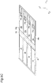
- FIG. 5 A a view showing a step in a method of manufacturing a wireless communication device.
- FIG. 5 B is a view showing a step following the step of FIG. 5 A .
- FIG. 5 C is a view showing a step following the step of FIG. 5 B .
- FIG. 5 D is a view showing a step following the step of FIG. 5 C .
- FIG. 5 E is a view showing a step following the step of FIG. 5 D .
- FIG. 6 is a partial cross-sectional view showing attachment of a connection conductor material to a base sheet material.
- FIG. 7 A is a side view of the wireless communication device with a base sheet folded at a longitudinal center.
- FIG. 7 B is a side view of the wireless communication device with the base sheet folded at a position shifted from the longitudinal center toward a first conductor pattern.
- FIG. 7 C is a side view of the wireless communication device with the base sheet folded at a position shifted from the longitudinal center toward a second conductor pattern.
- FIG. 8 is a perspective view of a wireless communication device according to another exemplary embodiment as viewed from the second principal surface side.
- FIG. 9 is a perspective view of a base sheet material in which a groove is formed.
- FIG. 10 is a perspective view of a wireless communication device according to a further exemplary embodiment.
- FIG. 11 is a partial cross-sectional view showing attachment of a connection conductor to a base sheet in a wireless communication device according to a different exemplary embodiment.
- FIG. 12 is a perspective view of an exemplary wireless communication device including a different first conductor pattern.
- FIG. 13 is a perspective view of another exemplary wireless communication device including a different first conductor pattern.
- FIG. 14 is a perspective view of a further exemplary wireless communication device including a different first conductor pattern.
- a wireless communication device in general, includes a base sheet in a folded state, a first conductor pattern disposed on a first principal surface of the base sheet, a second conductor pattern disposed on a second principal surface of the base sheet that is opposite to the first principal surface, an RFIC chip disposed on the base sheet and that is electrically connected to the first conductor pattern, and a sheet-shaped connection conductor affixed to a turning part of the base sheet so as to partially overlap with respective ends of the first and second conductor patterns that are near and/or adjacent to the turning part of the base sheet.
- occurrence of variations in communication characteristics can be suppressed in the wireless communication device that includes two conductor patterns opposite to each other and that is configured for of wireless communication even when attached to a metal surface of an article.
- connection conductor can be larger in at least one of thickness and width than the first and second conductor patterns. As a result, even if cracking occurs in the connection conductor, an influence on the communication characteristics of the wireless communication device can be reduced.
- portions of the base sheet facing each other can sandwich an interposed member having a permittivity lower than the base sheet.
- the wireless communication device can include an RFIC module including the RFIC chip and a matching circuit, such that the RFIC module is disposed on the base material so that the RFIC chip is electrically connected to the first conductor pattern via the matching circuit.
- the manufacturing method includes disposing a first conductor pattern and a second conductor pattern separately at an interval on the same surface of a base sheet, affixing a sheet-shaped connection conductor to a portion of the base sheet located between the first conductor pattern and the second conductor pattern so as to partially overlap with an end portion of the first conductor pattern and an end portion of the second conductor pattern separated at an interval, folding the base sheet together with the connection conductor between the first conductor pattern and the second conductor pattern with the first and second conductor patterns facing outward, affixing portions of the base sheet facing each other due to folding to each other, and disposing an RFIC chip on the base sheet so as to electrically connect to the first conductor pattern.
- occurrence of variations in communication characteristics can be suppressed in the wireless communication device that includes two conductor patterns opposite to each other and that is configured for wireless communication even when attached to a metal surface of an article.
- connection conductor can be larger in at least one of thickness and width than the first and second conductor patterns. As a result, even if cracking occurs in the connection conductor, an influence on the communication characteristics of the wireless communication device can be reduced.
- portions of the base sheet facing each other can sandwich an interposed member having a permittivity lower than the base sheet.
- the wireless communication device can include an RFIC module including the RFIC chip and a matching circuit, such that the RFIC module is disposed on the base material so that the RFIC chip is electrically connected to the first conductor pattern via the matching circuit.
- connection conductor can be affixed to the base sheet with an adhesive interposed therebetween, and the base sheet may be folded together with the connection conductor before completion of curing of the adhesive. As a result, occurrence of cracking in the connection conductor can be suppressed.
- the second conductor pattern can be larger than the first conductor pattern as viewed in a thickness direction of the base sheet. As a result, even if the folding position of the base sheet is shifted, the entire first conductor pattern can be opposite to the second conductor pattern. Therefore, a capacity between the first conductor pattern and the second conductor pattern can be maintained at a predetermined value, and variations in the communication characteristics of the wireless communication device can be suppressed.
- a groove can be disposed in a portion of the base sheet located between the first and second conductor patterns, and the base sheet may be folded along the groove. As a result, variations in the folding position of the base sheet are suppressed.
- the exemplary method of manufacturing a wireless communication device can further include arranging multiple sets of the first and second conductor patterns on a base sheet material side by side in a direction orthogonal to a direction of arrangement of the first conductor pattern and the corresponding second conductor pattern, affixing a belt-shaped connection conductor material to a portion of the base sheet material located between the first and second conductor patterns so as to partially overlap with an end portion of the first conductor pattern and an end portion of the second conductor pattern separated at an interval in each set, folding the base sheet material together with the connection conductor material between the first conductor pattern and the second conductor pattern in each set with the first and second conductor patterns facing outward, affixing portions of the base sheet material facing each other due to folding to each other, disposing a plurality of the RFIC chips on the base sheet material so as to respectively electrically connect to a plurality of the first conductor patterns, and cutting the base sheet material in a folded state provided with the plurality of the RFIC chips into a plurality
- the base sheet material may be a roll sheet.
- FIGS. 1 and 2 are perspective views showing a wireless communication device according to an exemplary embodiment of the present invention.
- the figures provide an X-Y-Z coordinate system for facilitating understanding of the invention and do not limit the invention.
- an X-axis direction indicates a width direction
- a Y-axis direction indicates a longitudinal direction
- a Z-axis direction indicates a thickness direction.
- a wireless communication device 10 is a so-called RFID (Radio-Frequency IDentification) tag and is the metal-compatible RFID tag 10 configured for wireless communication while being attached to a metal surface of an article such as a metal plate, for example.
- RFID Radio-Frequency IDentification
- the wireless communication device 10 includes a base sheet 12 and first and second conductor patterns 14 , 16 disposed on the base sheet 12 .
- the base sheet 12 also includes a connection conductor 18 electrically connecting the first and second conductor patterns 14 , 16 , and an RFIC (Radio-Frequency Integrated Circuit) module 30 electrically connected to the first conductor pattern 14 .
- RFIC Radio-Frequency Integrated Circuit
- the base sheet 12 is a sheet-shaped dielectric body, for example, a foamed PET (polyester) film having a thickness of 200 ⁇ m.
- the base sheet 12 is in a folded state. Specifically, the belt-shaped base sheet 12 is folded in two, and mutually facing parts thereof are affixed to each other by an insulating adhesive. Therefore, the base sheet 12 is formed into a substrate shape including a first principal surface 12 a and a second principal surface 12 b opposite to the first principal surface 12 a and including a turning part 12 c at one end in a longitudinal direction (i.e., the Y-axis direction).
- the base sheet 12 includes the U-shaped turning part 12 c and a pair of portions extending in substantially the same direction from both respective ends of the turning part 12 c and respectively including the first and second principal surfaces 12 a , 12 b.
- the first conductor pattern 14 is a rectangular conductor pattern disposed on the first principal surface 12 a of the base sheet 12 and is configured to function as a radiating part of the wireless communication device 10 .
- the first conductor pattern 14 is a pattern of aluminum or copper having a thickness of 5 to 30 ⁇ m.
- the first conductor pattern 14 is formed by etching on the first principal surface 12 a.
- the first conductor pattern 14 is made up of two parts. Specifically, the first conductor pattern 14 is made up of a first electrode part 14 a and a second electrode part 14 b surrounding the first electrode part 14 a . Specifically, the second electrode part 14 b accounts for most of the first conductor pattern 14 from perspective of total surface area of the first conductor pattern 14 .
- the second electrode part 14 b is provided with an opening part 14 c and a slit part 14 d extending from the opening part 14 c toward one end in the longitudinal direction (i.e., the Y-axis direction) (the end on the side farther from the turning part 12 c ).
- the first electrode part 14 a is disposed in the opening part 14 c separately at an interval from the second electrode part 14 b.
- the second conductor pattern 16 is a rectangular conductor pattern disposed on the second principal surface 12 b of the base sheet 12 and is configured to function as a connecting part electrically connecting to a metal surface of an article.
- the wireless communication device 10 when in a state of being attached to a metal surface of an article, the wireless communication device 10 is attached to the article with the second principal surface 12 b facing the metal surface of the article.
- the wireless communication device 10 is attached to the metal surface by using an insulating double-sided tape (not shown)
- the second conductor pattern 16 is capacitively connected (capacitively coupled) to the metal surface via the insulating double-sided tape.
- a conductive double-sided tape (not shown) is used, the second conductor pattern 16 is connected through a direct current to the metal surface of the article via the conductive double-sided tape.
- connection through a direct current means a connection allowing a direct current to flow between two objects (in this case, the second conductor pattern and the metal surface of the article).
- capactive connection means that although a direct current cannot flow between two objects, the two objects are capacitively coupled by a capacity formed between the two objects instead.
- electrical connection generally refers to either of a “connection through a direct current” and/or a “capacitive connection”.
- the second conductor pattern 16 is a pattern of aluminum or copper having a thickness of 5 to 30 ⁇ m as with the first conductor pattern 14 .
- the second conductor pattern 16 is formed by etching on the second principal surface 12 b.
- the second conductor pattern 16 is formed larger than the first conductor pattern 14 as viewed in the thickness direction (i.e., the Z-axis direction) of the base sheet 12 . Therefore, the second conductor pattern 16 is formed in a size such that the first conductor pattern 14 can be disposed within the contour of the second conductor pattern 16 when viewed in the thickness direction of the base sheet 12 . The reason will be described later.
- connection conductor 18 capacitively connects to each of the first and second conductor patterns 14 , 16 (i.e., a capacity is formed between the connection conductor 18 and the first conductor pattern 14 , and a capacity is formed between the connection conductor 18 and the second conductor pattern 16 ).
- connection conductor 18 has a sheet shape and is an aluminum film having a thickness of 50 ⁇ m, for example.
- the sheet-shaped connection conductor 18 is affixed to the turning part 12 c of the material sheet 12 so as to partially overlap with an end portion of the first conductor pattern 14 near the turning part 12 c and an end portion of the second conductor pattern 16 near the turning part 12 c .
- the connection conductor 18 is bonded to the base sheet 12 by an insulating adhesive such as an acrylic adhesive, for example.
- the width of the connection conductor 18 is larger than the widths of the first and second conductor patterns 14 , 16 .
- the width is a size in the direction (i.e., the X-axis direction) orthogonal to the direction of a current flowing sequentially through the first conductor pattern 14 , the connection conductor 18 , and the second conductor pattern 16 or the backward direction (i.e., the Y-axis direction).
- the thickness of the connection conductor 18 is larger than the thicknesses of the first and second conductor patterns 14 , 16 . The reason of making the width and thickness of the connection conductor 18 larger than those of the first and second conductor patterns 14 , 16 will be described later.
- the RFIC module 30 is a module including an RFIC chip and a matching circuit and is disposed on the first principal surface 12 a of the base sheet 12 .
- the RFIC module 30 is electrically connected to the first conductor pattern 14 , or specifically, in the case of this embodiment, the RFIC module 30 is connected through a direct current via solder etc.
- the RFIC module 30 will be described in more detail.
- FIG. 3 is an exploded perspective view of the RFIC module.
- FIG. 4 is an equivalent circuit diagram of the wireless communication device.
- the RFIC module 30 is a device that is configured to perform wireless communication at a predetermined communication frequency, for example, a communication frequency of, for example, the 900 MHz band, i.e., the UHF band.
- the RFIC module 30 is made up of a multilayer substrate composed of three layers. Specifically, the RFIC module 30 is formed by laminating flexible insulating sheets 32 A, 32 B, and 32 C made of a resin material such as polyimide and liquid crystal polymer.
- the RFIC module 30 has an RFIC (Radio-Frequency Integrated Circuit) chip 34 , a plurality of inductance elements 36 A, 36 B, 36 C, and 36 D, and external connection terminals 38 , 40 .
- the inductance elements 36 A to 36 D and the external connection terminals 38 , 40 are formed on the insulating sheets 32 A to 32 C and are made up of conductor patterns made of a conductive material such as copper.
- the RFIC chip 34 is mounted on a central part in the longitudinal direction (i.e., the Y-axis direction) on the insulating sheet 32 C.
- the RFIC chip 34 has a structure in which various elements are incorporated in a semiconductor substrate made of a semiconductor such as silicon.
- the RFIC chip 34 includes a first input/output terminal 34 a and a second input/output terminal 34 b .
- the RFIC chip 34 further includes an internal capacity (e.g., capacitance: a self-capacity of the RFIC chip itself) C 1 .
- the inductance element 36 A is made up of a conductor pattern disposed in a spiral coil shape on the insulating sheet 32 C on one side in the longitudinal direction (i.e., the Y-axis direction) of the insulating sheet 32 C.
- the inductance element 36 A includes an inductance L 1 .
- One end (e.g., an end on the coil outer side) of the inductance element 36 A is provided with a land 36 Aa connected to the first input/output terminal 34 a of the RFIC chip 34 .
- the other end e.g., an end on the coil center side
- the inductance element 36 B is made up of a conductor pattern disposed in a spiral coil shape on the insulating sheet 32 C on the other side in the longitudinal direction (i.e., the Y-axis direction) of the insulating sheet 32 C.
- the inductance element 36 B includes an inductance L 2 .
- One end (e.g., an end on the coil outer side) of the inductance element 36 B is provided with a land 36 Ba connected to the second input/output terminal 34 b of the RFIC chip 34 .
- the other end e.g., an end on the coil center side
- the inductance element 36 C is made up of a conductor pattern disposed in a spiral coil shape on the insulating sheet 32 B on one side in the longitudinal direction (i.e., the Y-axis direction) of the insulating sheet 32 B.
- the inductance element 36 C is opposite to the inductance element 36 A in the lamination direction (i.e., the Z-axis direction).
- the inductance element 36 C includes an inductance L 3 .
- One end (e.g., an end on the coil outer side) of the inductance element 36 C is provided with a land 36 Ca.
- the land 36 Ca is connected to the land 36 Ab of the inductance element 36 A on the insulating sheet 32 C via an interlayer connection conductor 42 such as a through-hole conductor penetrating the insulating sheet 32 B.
- the inductance element 36 D is made up of a conductor pattern disposed in a spiral coil shape on the insulating sheet 32 B on the other side in the longitudinal direction (Y-axis direction) of the insulating sheet 32 B.
- the inductance element 36 D is opposite to the inductance element 36 B in the lamination direction (i.e., the Z-axis direction).
- the inductance element 36 D includes an inductance L 4 .
- One end (e.g., an end on the coil outer side) of the inductance element 36 D is provided with a land 36 Da.
- the land 36 Da is connected to the land 36 Bb of the inductance element 36 B on the insulating sheet 32 C via an interlayer connection conductor 44 such as a through-hole conductor penetrating the insulating sheet 32 B.
- the inductance elements 36 C, 36 D on the insulating sheet 32 B are integrated as one conductor pattern. Specifically, the respective other ends (e.g., ends on the coil outer side) are connected to each other.
- the insulating sheet 32 B is provided with a through-hole 32 Ba in which the RFIC chip 34 mounted on the insulating sheet 32 C is received.
- the external connection terminals 38 , 40 are made up of conductor patterns disposed on the insulating sheet 32 A.
- the external connection terminals 38 , 40 are opposite in the longitudinal direction (i.e., the Y-axis direction) of the insulating sheet 32 A.
- the one external connection terminal 38 is connected to the land 36 Ca of the inductance element 36 C on the insulating sheet 32 B via an interlayer connection conductor 46 such as a through hole conductor penetrating the insulating sheet 32 A.
- the other external connection terminal 40 is connected to the land 36 Da of the inductance element 36 D on the insulating sheet 32 B via an interlayer connection conductor 48 such as a through hole conductor penetrating the insulating sheet 32 A.
- the one external connection terminal 38 is electrically connected via, for example, solder to the second electrode part 14 b of the first conductor pattern 14 .
- the other external connection terminal 40 is electrically connected via, for example, a solder to the first electrode part 14 a of the first conductor pattern 14 .
- the RFIC chip 34 is made up of a semiconductor substrate.
- the RFIC chip 34 is present between the inductance elements 36 A, 36 B and between the inductance elements 36 C, 36 D.
- the RFIC chip 34 functions as a shield, so that magnetic-field coupling and capacitive coupling are suppressed between the inductance elements 36 A, 37 B having the spiral coil shape disposed on the insulating sheet 32 C.
- magnetic-field coupling and capacitive coupling are suppressed between the inductance elements 36 C, 36 D having the spiral coil shape disposed on the insulating sheet 32 B.
- a passband of communication signals is prevented from narrowing.
- the capacity C 1 e.g., an internal capacity of the RFIC chip 34
- the inductances L 1 to L 4 e.g., inductances of four inductance elements
- the capacity C 1 e.g., an internal capacity of the RFIC chip 34
- the inductances L 1 to L 4 e.g., inductances of four inductance elements
- the wireless communication device 10 is configured to exchange radio waves with an external wireless communication apparatus (e.g., a reader/writer apparatus) substantially via the first conductor pattern 14 when the device is not attached to an article, or substantially via the first conductor pattern 14 and a metal surface Ms when the device is attached to the metal surface Ms as shown in FIG. 4 . Therefore, the metal surface Ms functions as an antenna.
- the second conductor pattern 16 is capacitively connected to the metal surface Ms (i.e., a capacity C 2 is formed therebetween).
- the RFIC chip 34 of the RFIC module 30 is driven by the electromotive force.
- the driven RFIC chip 34 transmits data stored in a storage part thereof via the first conductor pattern 14 or the metal surface Ms.
- the first conductor pattern 14 e.g., the first and second electrode parts 14 a , 14 b
- the second conductor pattern 16 are maintained at a constant distance (e.g., twice the thickness of the base sheet 12 ). Therefore, a capacity C 3 between the first electrode part 14 a of the first conductor pattern 14 and the second conductor pattern 16 is constant, and a capacity C 4 between the second electrode part 14 b and the second conductor pattern 16 is constant.
- the wireless communication device 10 is nearly unchanged in electrical characteristics, particularly in the capacities C 3 , C 4 as compared to before the connection.
- the resonance frequency of the wireless communication device 10 does not substantially change as compared to before attachment to the metal surface Ms.
- the metal surface Ms can be used as an antenna, so that the communication distance becomes longer.
- a method of manufacturing the wireless communication device 10 according to this embodiment will hereinafter be described.
- FIGS. 5 A to 5 E each show a step in a method of manufacturing a wireless communication device.
- a conductor layer 52 of aluminum, copper, etc. is formed on one entire surface 50 a of a base sheet material 50 .
- the base sheet material 50 is cut into multiple pieces in a later step and processed into the base sheet 12 of the wireless communication device 10 .
- the conductor layer 52 is processed by, for example, etching, into the first conductor pattern 14 (i.e., the first and second electrode parts 14 a , 14 b ) and the second conductor pattern 16 .
- the first conductor pattern 14 i.e., the first and second electrode parts 14 a , 14 b
- the second conductor pattern 16 i.e., four sets of the first and second conductor patterns 14 , 16 are formed. In each of the sets, the first conductor pattern 14 and the second conductor pattern 16 are disposed on the base sheet material 50 separately at an interval on the same surface.
- the multiple sets of the first and second conductor patterns 14 , 16 are arranged side by side in the direction (i.e., the X-axis direction) orthogonal to the direction (i.e., the Y-axis direction) of arrangement of the first conductor pattern 14 and the corresponding second conductor pattern 16 .
- connection conductor material 54 such as an aluminum film is affixed to the base sheet material 50 .
- the connection conductor material 54 is cut into multiple pieces in a later step and processed into the connection conductor 18 .
- FIG. 6 that is a partial cross-sectional view showing attachment of the connection conductor material to the base sheet material, the connection conductor material 54 is affixed via an insulating adhesive, such as an acrylic adhesive, or an insulating sticky material 56 .
- connection conductor material 54 is affixed via the insulating adhesive 56 in a portion of the base sheet material 50 located between the first and second conductor patterns 14 , 16 so as to partially overlap with an end portion of the first conductor pattern 14 and an end portion of the second conductor pattern 16 separated at an interval in each set. Consequently, as shown in FIG. 6 .
- connection conductor material 54 i.e., the connection conductor 18
- first conductor pattern 14 e.g., the second electrode part 14 b thereof
- connection conductor 18 and the second conductor pattern 16 are capacitively connected (i.e., a capacity C 6 is formed therebetween).
- the base sheet material 50 is folded together with the connection conductor material 54 between the first conductor pattern 14 and the second conductor pattern 16 in each set with the first and second conductor patterns 14 , 16 facing outward. Portions of the base sheet material 50 facing each other due to folding (i.e., the other folded surface 50 b ) are affixed to each other via an insulating adhesive.
- the base sheet material 50 is preferably folded together with the connection conductor material 54 before completion of curing of the adhesive.
- connection conductor material 54 is fixed to the base sheet material 50 by the completely cured adhesive and is therefore continuously subjected to a tensile force from the base sheet material 50 . Therefore, cracking easily occurs in the connection conductor material 54 .
- the base sheet material 50 is preferably folded together with the connection conductor material 54 before the adhesive is completely cured, i.e., while the connection conductor material 54 can slide relative to the base sheet material 50 .
- the occurrence of cracking in the connection conductor material 54 (the connection conductor 18 ) can advantageously be suppressed.
- the time until curing of the adhesive material becomes longer, so that the time after the affixing processing of the connection conductor material 54 until the folding processing can be made longer.
- the multiple RFIC modules 30 are disposed on the base sheet material 50 so as to electrically connect to the multiple respective first conductor patterns 14 .
- the base sheet material 50 in a folded state provided with the multiple RFIC modules 30 is cut into multiple pieces, and a plurality of the wireless communication devices 10 shown in FIGS. 1 and 2 is produced.
- the base sheet material 50 shown in FIGS. 5 A to 5 E is a cut sheet or may be a roll sheet.
- the steps shown in FIGS. 5 A to 5 E are performed in order on a sheet portion pulled out from the roll.
- the base sheet material 50 in a folded state provided with the multiple RFIC modules 30 may be wound into a roll again without being cut into multiple pieces.
- a method of folding a sheet portion pulled out from the roll in the width direction is not limited.
- occurrence of variations in communication characteristics can be suppressed in the wireless communication device that includes two conductor patterns opposite to each other and that is configured for wireless communication even when attached to a metal surface of an article.
- the first conductor pattern 14 on the first principal surface 12 a of the base sheet 12 and the second conductor pattern 16 on the second principal surface 12 b are electrically connected by the connection conductor 18 that is a member different therefrom.
- connection conductor 18 larger in width and thickness than the first and second conductor patterns 14 , 16 is usable. Additionally, the thickness of the connection conductor 18 can be made thicker than the first and second conductor patterns 14 , 16 to achieve a thickness at which an electrode hardly cracks due to folding, or the insulating adhesive 56 can be changed to the insulating sticky material to make the connection conductor 18 slidable during the folding processing so that no tensile stress is applied to the connection conductor 18 .
- a conductive film acquired by mixing a conductive filler with an elastic base material can be used as a material that is easily stretchable, i.e., a material that hardly cracks, as compared to the first and second conductor patterns 14 , 16 , for producing the connection conductor 18 .
- connection conductor 18 and the first and second conductor patterns 14 , 16 can capacitively be connected. As shown in FIG. 4 , by adjusting the capacities C 5 , C 6 generated therebetween, i.e., by adjusting the areas of the portions of the connection conductor 18 facing the first and second conductor patterns 14 , 16 , the communication frequency of the wireless communication device 10 can be adjusted.
- the occurrence of variations in communication characteristics can be suppressed in the multiple wireless communication devices 10 .
- the second conductor pattern 16 is formed larger than the first conductor pattern 14 as viewed in the thickness direction (i.e., the Z-axis direction) of the base sheet 12 . Therefore, even if variation occurs in the folding position, the capacities C 3 , C 4 between the first conductor pattern 14 and the second conductor pattern 16 can be maintained at predetermined values as shown in FIG. 4 . This will be specifically described.
- FIG. 7 A to 7 C each show a wireless communication device with a base sheet folded at a different position.
- FIG. 7 A shows the wireless communication device 10 with the base sheet 12 folded at the center in the longitudinal direction (i.e., the Y-axis direction), i.e., with both ends of the base sheet 12 made coincide on the side opposite to the turning part 12 c .
- the entire first conductor pattern 14 faces the second conductor pattern 16 .
- FIG. 7 B shows the wireless communication device 10 with the base sheet 12 folded at a position shifted toward the first conductor pattern 14 relative to the center in the longitudinal direction (i.e., the Y-axis direction), i.e., with both ends of the base sheet 12 shifted.
- the second conductor pattern 16 is formed larger than the first conductor pattern 14 , the entire first conductor pattern 14 can be opposite to the second conductor pattern 16 .
- FIG. 7 C shows the wireless communication device 10 with the base sheet 12 folded at a position shifted toward the second conductor pattern 16 relative to the center in the longitudinal direction (i.e., the Y-axis direction), i.e., with both ends of the base sheet 12 shifted.
- the second conductor pattern 16 is formed larger than the first conductor pattern 14 , the entire first conductor pattern 14 can be opposite to the second conductor pattern 16 .
- the second conductor pattern 16 is formed larger than the first conductor pattern 14 , so that the entire conductor pattern 14 can be opposite to the second conductor pattern 16 .
- the capacities C 3 , C 4 between the first conductor pattern 14 and the second conductor pattern 16 can be maintained at predetermined values. Consequently, the occurrence of variations in communication characteristics can be suppressed in the wireless communication device.
- the width (e.g., size in the X-axis direction) of the second conductor pattern 16 is preferably made larger than the width 18 of the first conductor pattern 14 .
- FIG. 8 shows a wireless communication device according to another embodiment as viewed from the second principal surface side.
- a second conductor pattern 116 is disposed over the entire second principal surface 12 b of the base sheet 12 .
- the entire first conductor pattern 14 can be opposite to the second conductor pattern 16 .
- the second conductor pattern 16 When the second conductor pattern 16 is enlarged, the second conductor pattern 16 and the metal surface Ms are strongly capacitively coupled while the wireless communication device 10 is attached to the metal surface Ms of the article via an insulating double-sided tape.
- the resistance between the second conductor pattern 16 and the metal surface Ms is reduced, and more current flows therebetween. As a result, stronger radio waves are emitted from the metal surface Ms, and consequently, the communication distance becomes longer.
- a groove can be disposed in the base sheet (i.e., the base sheet material) so as to suppress variation in folding, i.e., to suppress variation in the position of the first conductor pattern 14 with respect to the second conductor pattern 16 .
- FIG. 9 shows a base sheet material in which a groove is formed.
- a groove 50 c extending in the width direction (i.e., the X-axis direction) of the base sheet material 50 is formed in a portion of the one surface 50 a of the base sheet material 50 located between the first and second conductor patterns 14 , 16 .
- the groove 50 c is disposed at the center of the base sheet material 50 in the longitudinal direction (i.e., the Y-axis direction).
- the first and second conductor patterns 14 , 16 can have the same size as viewed in the thickness direction (i.e., the Z-axis direction) of the base sheet 12 (i.e., the base sheet material 50 ).
- the base sheet 12 i.e., the base sheet material 50
- the embodiments according to the present invention are not limited thereto.
- FIG. 10 shows a wireless communication device according to a further embodiment.
- the base sheet 12 is folded, and portions facing each other due to the folding sandwich an interposed member 220 .
- the interposed member 220 is a member having a permittivity lower than the base sheet 12 .
- the base sheet 12 is a foamed PET film having a permittivity of about 2.0
- the interposed member 220 is a foamed olefin film having a permittivity of about 1.1, for example.
- the interposed member 220 is a member made of the same material as the base sheet 12 and having a foaming ratio higher than the base sheet 12 .
- the interposed member 220 having a permittivity lower than the base sheet 12 can reduce the capacities C 3 , C 4 between the first conductor pattern 14 and the second conductor pattern 16 . Consequently, the communication distance of the wireless communication device 210 becomes longer as compared to when the interposed member 220 is not present.
- the base sheet is not limited to being folded in two and may be folded in three. As the number of overlaps of the base sheet increases, the capacity can be made smaller between the first conductor pattern and the second conductor pattern.
- connection conductor material 54 i.e., the connection conductor 18
- base sheet material 50 i.e., the base sheet 12
- insulating adhesive 56 interposed therebetween.
- the embodiments according to the present invention are not limited thereto.
- FIG. 11 is a partial cross-sectional view showing attachment of a connection conductor to a base sheet in a wireless communication device according to a different embodiment.
- connection conductor 18 i.e., the connection conductor material 54
- base sheet 12 i.e., the base sheet material 50
- an insulating or conductive paste 322 interposed therebetween. Therefore, although electrically connected to the first and second conductor patterns 14 , 16 , the connection conductor 18 is not fixed and is slidable.
- a cover member 324 overlaps the connection conductor 18 so as to maintain the electrical connection between the connection conductor 18 and the first and second conductor patterns 14 , 16 .
- An outer circumferential edge of the cover member 324 is affixed to the base sheet 12 and the first and second conductor patterns 14 , 16 with an insulating adhesive 326 interposed therebetween.
- the cover member 324 and the connection conductor 18 are not bonded to each other and are in contact with each other.
- connection conductor 18 According to the affixing of the connection conductor 18 to the base sheet 12 as described above, when the base sheet 12 is folded together with the connection conductor 18 , the connection conductor 18 slides relative to the base sheet 12 and the cover member 324 . Since the connection conductor 18 is not fixed to the base sheet 12 or the cover member 324 , the connection conductor 18 hardly cracks after being folded.
- connection conductor the sheet-shaped connection conductor electrically connecting the first conductor pattern and the second conductor pattern is preferably made up of a single conductor of aluminum etc.
- the sheet-shaped connection conductor may be a conductor produced by forming a conductor layer on a sheet-shaped member such as a resin film.
- the connection conductor can be folded with the conductor layer facing inside so that the resin film is located in an outermost circumferential portion having a maximum point of tensile stress, and therefore, the occurrence of cracking of the conductive layer can be suppressed.
- the exemplary embodiments according to the present invention do not limit the form of the first conductor pattern functioning as the radiating part.
- FIGS. 12 to 14 each show a wireless communication device including a different first conductor pattern.
- a first conductor pattern 414 is rectangular and includes an opening part 414 a and a slit part 414 b extending from the opening part 414 a toward one end in the longitudinal direction (i.e., the Y-axis direction) (the end on the side farther from the turning part 12 c of the base sheet 12 ).
- the RFIC module 30 is disposed on the first conductor pattern 414 so as to straddle the slit part 414 b .
- the external connection terminals 38 , 40 of the RFIC module 30 are electrically connected to two respective portions of the first conductor patterns 414 facing each other across the slit part 414 b.
- a first conductor pattern 514 is made up of two parts.
- the first conductor pattern 514 includes a belt-shaped conductor pattern 514 a and a loop-shaped conductor pattern 514 b .
- the loop-shaped conductor pattern 514 b is C-shaped, and both ends thereof are respectively electrically connected to the external connection terminals 38 , 40 of the RFIC module 30 .
- the loop-shaped conductor pattern 514 b is partially overlapped with the belt-shaped conductor pattern 514 a for electrically connecting to the belt-shaped conductor pattern 514 a .
- the communication characteristics, for example, the frequency band, of the wireless communication device 510 can be adjusted.
- a first conductor pattern 614 is composed of two parts. Specifically, the first conductor pattern 614 includes a belt-shaped conductor pattern 614 a and a T-shaped conductor pattern 614 b .
- the T-shaped conductor pattern 614 b includes a belt-shaped part 614 c extending in the width direction (i.e., the X-axis direction) of the wireless communication device 610 .
- One of the external connection terminals 38 , 40 of the RFIC module 30 is electrically connected to a central portion of the belt-shaped part 614 c .
- the other external connection terminal of the RFIC module 30 is electrically connected to one end in the longitudinal direction (i.e., the Y-axis direction) of the belt-shaped conductor pattern 614 a (e.g., the end on the side farther from the turning part 12 c of the base sheet 12 ).
- a wireless communication device includes a base sheet in a folded state, a first conductor pattern disposed on a first principal surface of the base sheet, a second conductor pattern disposed on a second principal surface of the base sheet opposite to the first principal surface, an RFIC chip disposed on the base sheet so as to electrically connect to the first conductor pattern, and a sheet-shaped connection conductor affixed to a turning part of the base sheet so as to partially overlap with an end portion of the first conductor pattern near the turning part and an end portion of the second conductor pattern near the turning part.
- a method of manufacturing a wireless communication device includes disposing a first conductor pattern and a second conductor pattern separately at an interval on the same surface of a base sheet, affixing a sheet-shaped connection conductor to a portion of the base sheet located between the first conductor pattern and the second conductor pattern so as to partially overlap with an end portion of the first conductor pattern and an end portion of the second conductor pattern separated at an interval, folding the base sheet together with the connection conductor between the first conductor pattern and the second conductor pattern with the first and second conductor patterns facing outward, affixing portions of the base sheet facing each other due to folding to each other, and disposing an RFIC chip on the base sheet so as to electrically connect to the first conductor pattern.
Landscapes
- Engineering & Computer Science (AREA)
- Microelectronics & Electronic Packaging (AREA)
- Manufacturing & Machinery (AREA)
- Computer Networks & Wireless Communication (AREA)
- Signal Processing (AREA)
- Details Of Aerials (AREA)
- Transceivers (AREA)
Abstract
Description
-
- 10 wireless communication device
- 12 base sheet
- 12 a first principal surface
- 12 b second principal surface
- 12 c turning part
- 14 first conductor pattern
- 18 connection conductor
- 30 RFIC module
Claims (20)
Applications Claiming Priority (4)
| Application Number | Priority Date | Filing Date | Title |
|---|---|---|---|
| JP2018-132909 | 2018-07-13 | ||
| JPJP2018-132909 | 2018-07-13 | ||
| JP2018132909 | 2018-07-13 | ||
| PCT/JP2019/012481 WO2020012726A1 (en) | 2018-07-13 | 2019-03-25 | Wireless communication device and method for producing same |
Related Parent Applications (1)
| Application Number | Title | Priority Date | Filing Date |
|---|---|---|---|
| PCT/JP2019/012481 Continuation WO2020012726A1 (en) | 2018-07-13 | 2019-03-25 | Wireless communication device and method for producing same |
Publications (2)
| Publication Number | Publication Date |
|---|---|
| US20200045821A1 US20200045821A1 (en) | 2020-02-06 |
| US11546993B2 true US11546993B2 (en) | 2023-01-03 |
Family
ID=69142838
Family Applications (1)
| Application Number | Title | Priority Date | Filing Date |
|---|---|---|---|
| US16/595,897 Active 2040-05-21 US11546993B2 (en) | 2018-07-13 | 2019-10-08 | Wireless communication device and method of manufacturing same |
Country Status (4)
| Country | Link |
|---|---|
| US (1) | US11546993B2 (en) |
| CN (1) | CN211236956U (en) |
| DE (1) | DE212019000090U1 (en) |
| WO (1) | WO2020012726A1 (en) |
Citations (15)
| Publication number | Priority date | Publication date | Assignee | Title |
|---|---|---|---|---|
| JP2005191705A (en) | 2003-12-24 | 2005-07-14 | Sharp Corp | Wireless tag and RFID system using the same |
| US20050230852A1 (en) * | 2004-04-20 | 2005-10-20 | Hee-Seok Lee | Semiconductor chip package |
| US20060032926A1 (en) * | 2004-08-13 | 2006-02-16 | Fujitsu Limited | Radio frequency identification (RFID) tag and manufacturing method thereof |
| US20060145872A1 (en) * | 2004-12-16 | 2006-07-06 | Denso Corporation | IC tag and IC tag attachment structure |
| US20090224061A1 (en) * | 2007-05-10 | 2009-09-10 | Murata Manufacturing Co., Ltd. | Wireless ic device |
| US20110048771A1 (en) * | 2009-08-26 | 2011-03-03 | Fujitsu Limited | Electronic apparatus and flexible substrate wiring method |
| JP2011159212A (en) | 2010-02-03 | 2011-08-18 | Toppan Forms Co Ltd | Noncontact data transmission/reception object and heavy load detector using the same |
| US20110279326A1 (en) * | 2010-05-14 | 2011-11-17 | Murata Manufacturing Co., Ltd. | Wireless ic device |
| US20120074229A1 (en) * | 2009-06-03 | 2012-03-29 | Murata Manufacturing Co., Ltd. | Radio frequency ic device and method of manufacturing the same |
| JP2014071585A (en) | 2012-09-28 | 2014-04-21 | Sato Holdings Corp | Rfid tag, rfid tag continuous body, and rfid tag manufacturing method |
| US20140254111A1 (en) * | 2013-03-07 | 2014-09-11 | Semiconductor Energy Laboratory Co., Ltd. | Display device |
| US20150351222A1 (en) * | 2013-03-26 | 2015-12-03 | Murata Manufacturing Co., Ltd. | Resin multilayer substrate and electronic apparatus |
| US20170017873A1 (en) * | 2015-07-15 | 2017-01-19 | Fujitsu Limited | Substrate, wireless tag, and electronic device |
| US20180032853A1 (en) | 2015-02-10 | 2018-02-01 | Phoenix Solution Co., Ltd. | Rf tag antenna and method for manufacturing same, and rf tag |
| US10726322B2 (en) * | 2015-07-21 | 2020-07-28 | Murata Manufacturing Co., Ltd. | Wireless communication device and article equipped with the same |
Family Cites Families (1)
| Publication number | Priority date | Publication date | Assignee | Title |
|---|---|---|---|---|
| JPS5170156A (en) | 1974-12-14 | 1976-06-17 | Kobe Steel Ltd | YOSETSUYOKONTAKUTOCHITSUPU |
-
2019
- 2019-03-25 DE DE212019000090.8U patent/DE212019000090U1/en active Active
- 2019-03-25 CN CN201990000156.6U patent/CN211236956U/en active Active
- 2019-03-25 WO PCT/JP2019/012481 patent/WO2020012726A1/en not_active Ceased
- 2019-10-08 US US16/595,897 patent/US11546993B2/en active Active
Patent Citations (19)
| Publication number | Priority date | Publication date | Assignee | Title |
|---|---|---|---|---|
| JP2005191705A (en) | 2003-12-24 | 2005-07-14 | Sharp Corp | Wireless tag and RFID system using the same |
| US20050230852A1 (en) * | 2004-04-20 | 2005-10-20 | Hee-Seok Lee | Semiconductor chip package |
| US20060032926A1 (en) * | 2004-08-13 | 2006-02-16 | Fujitsu Limited | Radio frequency identification (RFID) tag and manufacturing method thereof |
| US20060145872A1 (en) * | 2004-12-16 | 2006-07-06 | Denso Corporation | IC tag and IC tag attachment structure |
| US20090224061A1 (en) * | 2007-05-10 | 2009-09-10 | Murata Manufacturing Co., Ltd. | Wireless ic device |
| US20120074229A1 (en) * | 2009-06-03 | 2012-03-29 | Murata Manufacturing Co., Ltd. | Radio frequency ic device and method of manufacturing the same |
| US20110048771A1 (en) * | 2009-08-26 | 2011-03-03 | Fujitsu Limited | Electronic apparatus and flexible substrate wiring method |
| JP2011159212A (en) | 2010-02-03 | 2011-08-18 | Toppan Forms Co Ltd | Noncontact data transmission/reception object and heavy load detector using the same |
| JP2011244110A (en) | 2010-05-14 | 2011-12-01 | Murata Mfg Co Ltd | Wireless ic device |
| US20110279326A1 (en) * | 2010-05-14 | 2011-11-17 | Murata Manufacturing Co., Ltd. | Wireless ic device |
| JP5170156B2 (en) | 2010-05-14 | 2013-03-27 | 株式会社村田製作所 | Wireless IC device |
| US9123996B2 (en) | 2010-05-14 | 2015-09-01 | Murata Manufacturing Co., Ltd. | Wireless IC device |
| JP2014071585A (en) | 2012-09-28 | 2014-04-21 | Sato Holdings Corp | Rfid tag, rfid tag continuous body, and rfid tag manufacturing method |
| US20140254111A1 (en) * | 2013-03-07 | 2014-09-11 | Semiconductor Energy Laboratory Co., Ltd. | Display device |
| US20150351222A1 (en) * | 2013-03-26 | 2015-12-03 | Murata Manufacturing Co., Ltd. | Resin multilayer substrate and electronic apparatus |
| US20180032853A1 (en) | 2015-02-10 | 2018-02-01 | Phoenix Solution Co., Ltd. | Rf tag antenna and method for manufacturing same, and rf tag |
| JP2018061275A (en) | 2015-02-10 | 2018-04-12 | 株式会社フェニックスソリューション | RF tag antenna, manufacturing method thereof, and RF tag |
| US20170017873A1 (en) * | 2015-07-15 | 2017-01-19 | Fujitsu Limited | Substrate, wireless tag, and electronic device |
| US10726322B2 (en) * | 2015-07-21 | 2020-07-28 | Murata Manufacturing Co., Ltd. | Wireless communication device and article equipped with the same |
Non-Patent Citations (3)
| Title |
|---|
| International Search Report issued for PCT/JP2019/012481, dated Jun. 11, 2019 (Japanese language). |
| International Search Report issued for PCT/JP2019/012481, dated Jun. 11, 2019. |
| Written Opinion of the International Searching Authority issued for PCT/JP2019/012481, dated Jun. 11, 2019. |
Also Published As
| Publication number | Publication date |
|---|---|
| DE212019000090U1 (en) | 2019-12-16 |
| US20200045821A1 (en) | 2020-02-06 |
| CN211236956U (en) | 2020-08-11 |
| WO2020012726A1 (en) | 2020-01-16 |
Similar Documents
| Publication | Publication Date | Title |
|---|---|---|
| US11641714B2 (en) | RFID tag | |
| US10971796B2 (en) | Wireless communication device | |
| US10108896B2 (en) | RFIC module and RFID tag including the same | |
| US9123996B2 (en) | Wireless IC device | |
| US10210449B2 (en) | Wireless communication device, method for manufacturing same, seal fitted with RFIC element, and method for producing same | |
| US9627759B2 (en) | Antenna device antenna module | |
| US10396429B2 (en) | Wireless communication device | |
| US7924228B2 (en) | Storage medium with built-in antenna | |
| US11100382B2 (en) | Card-type wireless communication device | |
| US11875210B2 (en) | Wireless communication device and method of manufacturing same | |
| US8937576B2 (en) | Wireless communication device | |
| US11114392B2 (en) | Wireless communication device | |
| US10467516B2 (en) | Component built-in device | |
| US10726322B2 (en) | Wireless communication device and article equipped with the same | |
| US10262252B2 (en) | Wireless communication device and article equipped with the same | |
| US11546993B2 (en) | Wireless communication device and method of manufacturing same | |
| CN215932657U (en) | RFIC module and RFID tag | |
| JP6610850B1 (en) | Wireless communication device and manufacturing method thereof | |
| US20220253665A1 (en) | Rfid tag roll | |
| CN118572351A (en) | Antenna device and IC card provided with same | |
| JP2024122288A (en) | Antenna device and IC card equipped with same |
Legal Events
| Date | Code | Title | Description |
|---|---|---|---|
| AS | Assignment |
Owner name: MURATA MANUFACTURING CO., LTD., JAPAN Free format text: ASSIGNMENT OF ASSIGNORS INTEREST;ASSIGNOR:KATO, NOBORU;REEL/FRAME:050653/0794 Effective date: 20191002 |
|
| FEPP | Fee payment procedure |
Free format text: ENTITY STATUS SET TO UNDISCOUNTED (ORIGINAL EVENT CODE: BIG.); ENTITY STATUS OF PATENT OWNER: LARGE ENTITY |
|
| STPP | Information on status: patent application and granting procedure in general |
Free format text: DOCKETED NEW CASE - READY FOR EXAMINATION |
|
| STPP | Information on status: patent application and granting procedure in general |
Free format text: NON FINAL ACTION MAILED |
|
| STPP | Information on status: patent application and granting procedure in general |
Free format text: NON FINAL ACTION MAILED |
|
| STPP | Information on status: patent application and granting procedure in general |
Free format text: RESPONSE TO NON-FINAL OFFICE ACTION ENTERED AND FORWARDED TO EXAMINER |
|
| STPP | Information on status: patent application and granting procedure in general |
Free format text: FINAL REJECTION MAILED |
|
| STPP | Information on status: patent application and granting procedure in general |
Free format text: DOCKETED NEW CASE - READY FOR EXAMINATION |
|
| STPP | Information on status: patent application and granting procedure in general |
Free format text: NOTICE OF ALLOWANCE MAILED -- APPLICATION RECEIVED IN OFFICE OF PUBLICATIONS |
|
| STPP | Information on status: patent application and granting procedure in general |
Free format text: PUBLICATIONS -- ISSUE FEE PAYMENT VERIFIED |
|
| STCF | Information on status: patent grant |
Free format text: PATENTED CASE |