US11527703B2 - Multi-layered piezoelectric ceramic-containing structure - Google Patents
Multi-layered piezoelectric ceramic-containing structure Download PDFInfo
- Publication number
- US11527703B2 US11527703B2 US16/769,120 US201816769120A US11527703B2 US 11527703 B2 US11527703 B2 US 11527703B2 US 201816769120 A US201816769120 A US 201816769120A US 11527703 B2 US11527703 B2 US 11527703B2
- Authority
- US
- United States
- Prior art keywords
- layer
- piezoelectric ceramic
- metallic
- thermal barrier
- depositing
- Prior art date
- Legal status (The legal status is an assumption and is not a legal conclusion. Google has not performed a legal analysis and makes no representation as to the accuracy of the status listed.)
- Active, expires
Links
- 239000000919 ceramic Substances 0.000 title claims abstract description 113
- 239000010410 layer Substances 0.000 claims abstract description 252
- 239000000758 substrate Substances 0.000 claims abstract description 77
- 230000004888 barrier function Effects 0.000 claims abstract description 64
- 239000012790 adhesive layer Substances 0.000 claims abstract description 59
- 229910052751 metal Inorganic materials 0.000 claims abstract description 56
- 239000002184 metal Substances 0.000 claims abstract description 56
- 238000000034 method Methods 0.000 claims abstract description 46
- 238000000151 deposition Methods 0.000 claims description 51
- 238000007751 thermal spraying Methods 0.000 claims description 16
- 229910045601 alloy Inorganic materials 0.000 claims description 12
- 239000000956 alloy Substances 0.000 claims description 12
- MCMNRKCIXSYSNV-UHFFFAOYSA-N Zirconium dioxide Chemical compound O=[Zr]=O MCMNRKCIXSYSNV-UHFFFAOYSA-N 0.000 claims description 10
- 229910000831 Steel Inorganic materials 0.000 claims description 9
- 239000010959 steel Substances 0.000 claims description 9
- 239000010953 base metal Substances 0.000 claims description 3
- FSAJRXGMUISOIW-UHFFFAOYSA-N bismuth sodium Chemical compound [Na].[Bi] FSAJRXGMUISOIW-UHFFFAOYSA-N 0.000 claims description 3
- 229910052809 inorganic oxide Inorganic materials 0.000 claims description 3
- 229910001092 metal group alloy Inorganic materials 0.000 claims description 3
- BITYAPCSNKJESK-UHFFFAOYSA-N potassiosodium Chemical group [Na].[K] BITYAPCSNKJESK-UHFFFAOYSA-N 0.000 claims description 3
- 239000011734 sodium Substances 0.000 description 24
- 229910052708 sodium Inorganic materials 0.000 description 20
- 238000010438 heat treatment Methods 0.000 description 15
- KDLHZDBZIXYQEI-UHFFFAOYSA-N Palladium Chemical compound [Pd] KDLHZDBZIXYQEI-UHFFFAOYSA-N 0.000 description 13
- 239000010935 stainless steel Substances 0.000 description 13
- 229910001220 stainless steel Inorganic materials 0.000 description 13
- 239000000203 mixture Substances 0.000 description 12
- 239000002245 particle Substances 0.000 description 8
- 239000007921 spray Substances 0.000 description 8
- 239000000463 material Substances 0.000 description 7
- BASFCYQUMIYNBI-UHFFFAOYSA-N platinum Chemical compound [Pt] BASFCYQUMIYNBI-UHFFFAOYSA-N 0.000 description 7
- PXHVJJICTQNCMI-UHFFFAOYSA-N Nickel Chemical compound [Ni] PXHVJJICTQNCMI-UHFFFAOYSA-N 0.000 description 6
- PNEYBMLMFCGWSK-UHFFFAOYSA-N aluminium oxide Inorganic materials [O-2].[O-2].[O-2].[Al+3].[Al+3] PNEYBMLMFCGWSK-UHFFFAOYSA-N 0.000 description 6
- 238000000576 coating method Methods 0.000 description 6
- 230000032798 delamination Effects 0.000 description 6
- 239000000843 powder Substances 0.000 description 6
- 238000004140 cleaning Methods 0.000 description 5
- 238000007750 plasma spraying Methods 0.000 description 5
- 238000007788 roughening Methods 0.000 description 5
- 238000005524 ceramic coating Methods 0.000 description 4
- 230000007797 corrosion Effects 0.000 description 4
- 238000005260 corrosion Methods 0.000 description 4
- 230000008021 deposition Effects 0.000 description 4
- 230000000694 effects Effects 0.000 description 4
- 238000009501 film coating Methods 0.000 description 4
- 230000003647 oxidation Effects 0.000 description 4
- 238000007254 oxidation reaction Methods 0.000 description 4
- 229910052574 oxide ceramic Inorganic materials 0.000 description 4
- 238000010422 painting Methods 0.000 description 4
- 239000002243 precursor Substances 0.000 description 4
- 230000008569 process Effects 0.000 description 4
- 238000007669 thermal treatment Methods 0.000 description 4
- 238000010290 vacuum plasma spraying Methods 0.000 description 4
- VYPSYNLAJGMNEJ-UHFFFAOYSA-N Silicium dioxide Chemical compound O=[Si]=O VYPSYNLAJGMNEJ-UHFFFAOYSA-N 0.000 description 3
- 238000000137 annealing Methods 0.000 description 3
- 230000008901 benefit Effects 0.000 description 3
- 229910010293 ceramic material Inorganic materials 0.000 description 3
- 239000011248 coating agent Substances 0.000 description 3
- 230000005684 electric field Effects 0.000 description 3
- 239000000446 fuel Substances 0.000 description 3
- 239000007769 metal material Substances 0.000 description 3
- 239000011224 oxide ceramic Substances 0.000 description 3
- 229910052763 palladium Inorganic materials 0.000 description 3
- 238000002360 preparation method Methods 0.000 description 3
- 229910052709 silver Inorganic materials 0.000 description 3
- 238000005507 spraying Methods 0.000 description 3
- 239000010936 titanium Substances 0.000 description 3
- 229910001316 Ag alloy Inorganic materials 0.000 description 2
- LFQSCWFLJHTTHZ-UHFFFAOYSA-N Ethanol Chemical compound CCO LFQSCWFLJHTTHZ-UHFFFAOYSA-N 0.000 description 2
- 229910001252 Pd alloy Inorganic materials 0.000 description 2
- KJTLSVCANCCWHF-UHFFFAOYSA-N Ruthenium Chemical compound [Ru] KJTLSVCANCCWHF-UHFFFAOYSA-N 0.000 description 2
- CDBYLPFSWZWCQE-UHFFFAOYSA-L Sodium Carbonate Chemical compound [Na+].[Na+].[O-]C([O-])=O CDBYLPFSWZWCQE-UHFFFAOYSA-L 0.000 description 2
- RTAQQCXQSZGOHL-UHFFFAOYSA-N Titanium Chemical compound [Ti] RTAQQCXQSZGOHL-UHFFFAOYSA-N 0.000 description 2
- 238000002441 X-ray diffraction Methods 0.000 description 2
- QVGXLLKOCUKJST-UHFFFAOYSA-N atomic oxygen Chemical compound [O] QVGXLLKOCUKJST-UHFFFAOYSA-N 0.000 description 2
- 230000001680 brushing effect Effects 0.000 description 2
- 239000001273 butane Substances 0.000 description 2
- 238000005336 cracking Methods 0.000 description 2
- 238000003618 dip coating Methods 0.000 description 2
- 238000005516 engineering process Methods 0.000 description 2
- 239000010408 film Substances 0.000 description 2
- 239000007888 film coating Substances 0.000 description 2
- 239000007789 gas Substances 0.000 description 2
- 239000010931 gold Substances 0.000 description 2
- 230000036541 health Effects 0.000 description 2
- 238000007641 inkjet printing Methods 0.000 description 2
- 238000004519 manufacturing process Methods 0.000 description 2
- 238000012544 monitoring process Methods 0.000 description 2
- IJDNQMDRQITEOD-UHFFFAOYSA-N n-butane Chemical compound CCCC IJDNQMDRQITEOD-UHFFFAOYSA-N 0.000 description 2
- OFBQJSOFQDEBGM-UHFFFAOYSA-N n-pentane Natural products CCCCC OFBQJSOFQDEBGM-UHFFFAOYSA-N 0.000 description 2
- 229910052759 nickel Inorganic materials 0.000 description 2
- ZKATWMILCYLAPD-UHFFFAOYSA-N niobium pentoxide Chemical compound O=[Nb](=O)O[Nb](=O)=O ZKATWMILCYLAPD-UHFFFAOYSA-N 0.000 description 2
- 239000001301 oxygen Substances 0.000 description 2
- 229910052760 oxygen Inorganic materials 0.000 description 2
- 229910052697 platinum Inorganic materials 0.000 description 2
- BWHMMNNQKKPAPP-UHFFFAOYSA-L potassium carbonate Chemical compound [K+].[K+].[O-]C([O-])=O BWHMMNNQKKPAPP-UHFFFAOYSA-L 0.000 description 2
- 238000003672 processing method Methods 0.000 description 2
- 239000010948 rhodium Substances 0.000 description 2
- 229910052707 ruthenium Inorganic materials 0.000 description 2
- 238000007650 screen-printing Methods 0.000 description 2
- 230000007847 structural defect Effects 0.000 description 2
- 239000010409 thin film Substances 0.000 description 2
- 229910052719 titanium Inorganic materials 0.000 description 2
- RYGMFSIKBFXOCR-UHFFFAOYSA-N Copper Chemical compound [Cu] RYGMFSIKBFXOCR-UHFFFAOYSA-N 0.000 description 1
- XEEYBQQBJWHFJM-UHFFFAOYSA-N Iron Chemical compound [Fe] XEEYBQQBJWHFJM-UHFFFAOYSA-N 0.000 description 1
- 229910019606 La0.5Sr0.5CoO3 Inorganic materials 0.000 description 1
- 229910002182 La0.7Sr0.3MnO3 Inorganic materials 0.000 description 1
- 229910002340 LaNiO3 Inorganic materials 0.000 description 1
- NPXOKRUENSOPAO-UHFFFAOYSA-N Raney nickel Chemical compound [Al].[Ni] NPXOKRUENSOPAO-UHFFFAOYSA-N 0.000 description 1
- XUIMIQQOPSSXEZ-UHFFFAOYSA-N Silicon Chemical compound [Si] XUIMIQQOPSSXEZ-UHFFFAOYSA-N 0.000 description 1
- BQCADISMDOOEFD-UHFFFAOYSA-N Silver Chemical compound [Ag] BQCADISMDOOEFD-UHFFFAOYSA-N 0.000 description 1
- 239000000443 aerosol Substances 0.000 description 1
- 229910052782 aluminium Inorganic materials 0.000 description 1
- 239000004411 aluminium Substances 0.000 description 1
- XAGFODPZIPBFFR-UHFFFAOYSA-N aluminium Chemical compound [Al] XAGFODPZIPBFFR-UHFFFAOYSA-N 0.000 description 1
- LJCFOYOSGPHIOO-UHFFFAOYSA-N antimony pentoxide Inorganic materials O=[Sb](=O)O[Sb](=O)=O LJCFOYOSGPHIOO-UHFFFAOYSA-N 0.000 description 1
- 238000000224 chemical solution deposition Methods 0.000 description 1
- 229910017052 cobalt Inorganic materials 0.000 description 1
- 239000010941 cobalt Substances 0.000 description 1
- GUTLYIVDDKVIGB-UHFFFAOYSA-N cobalt atom Chemical compound [Co] GUTLYIVDDKVIGB-UHFFFAOYSA-N 0.000 description 1
- 229910052681 coesite Inorganic materials 0.000 description 1
- 239000010949 copper Substances 0.000 description 1
- 229910052802 copper Inorganic materials 0.000 description 1
- 230000008878 coupling Effects 0.000 description 1
- 238000010168 coupling process Methods 0.000 description 1
- 238000005859 coupling reaction Methods 0.000 description 1
- 229910052906 cristobalite Inorganic materials 0.000 description 1
- 238000006073 displacement reaction Methods 0.000 description 1
- 238000010304 firing Methods 0.000 description 1
- PCHJSUWPFVWCPO-UHFFFAOYSA-N gold Chemical compound [Au] PCHJSUWPFVWCPO-UHFFFAOYSA-N 0.000 description 1
- 229910052737 gold Inorganic materials 0.000 description 1
- 229910052808 lithium carbonate Inorganic materials 0.000 description 1
- XGZVUEUWXADBQD-UHFFFAOYSA-L lithium carbonate Chemical compound [Li+].[Li+].[O-]C([O-])=O XGZVUEUWXADBQD-UHFFFAOYSA-L 0.000 description 1
- 150000002739 metals Chemical class 0.000 description 1
- 239000004570 mortar (masonry) Substances 0.000 description 1
- 229910000907 nickel aluminide Inorganic materials 0.000 description 1
- 229910052700 potassium Inorganic materials 0.000 description 1
- 229910000027 potassium carbonate Inorganic materials 0.000 description 1
- 229910052761 rare earth metal Inorganic materials 0.000 description 1
- 229910001404 rare earth metal oxide Inorganic materials 0.000 description 1
- 150000002910 rare earth metals Chemical class 0.000 description 1
- 230000004044 response Effects 0.000 description 1
- 229910052703 rhodium Inorganic materials 0.000 description 1
- MHOVAHRLVXNVSD-UHFFFAOYSA-N rhodium atom Chemical compound [Rh] MHOVAHRLVXNVSD-UHFFFAOYSA-N 0.000 description 1
- 238000005488 sandblasting Methods 0.000 description 1
- 238000001878 scanning electron micrograph Methods 0.000 description 1
- 238000004626 scanning electron microscopy Methods 0.000 description 1
- 229910052710 silicon Inorganic materials 0.000 description 1
- 239000010703 silicon Substances 0.000 description 1
- 239000000377 silicon dioxide Substances 0.000 description 1
- 239000004332 silver Substances 0.000 description 1
- 239000002002 slurry Substances 0.000 description 1
- 229910000029 sodium carbonate Inorganic materials 0.000 description 1
- 239000007787 solid Substances 0.000 description 1
- 238000009718 spray deposition Methods 0.000 description 1
- 238000004544 sputter deposition Methods 0.000 description 1
- 239000007858 starting material Substances 0.000 description 1
- 229910052682 stishovite Inorganic materials 0.000 description 1
- PBCFLUZVCVVTBY-UHFFFAOYSA-N tantalum pentoxide Inorganic materials O=[Ta](=O)O[Ta](=O)=O PBCFLUZVCVVTBY-UHFFFAOYSA-N 0.000 description 1
- 229910052905 tridymite Inorganic materials 0.000 description 1
- 229910001233 yttria-stabilized zirconia Inorganic materials 0.000 description 1
- 229910052727 yttrium Inorganic materials 0.000 description 1
Images


Classifications
-
- H—ELECTRICITY
- H10—SEMICONDUCTOR DEVICES; ELECTRIC SOLID-STATE DEVICES NOT OTHERWISE PROVIDED FOR
- H10N—ELECTRIC SOLID-STATE DEVICES NOT OTHERWISE PROVIDED FOR
- H10N30/00—Piezoelectric or electrostrictive devices
- H10N30/704—Piezoelectric or electrostrictive devices based on piezoelectric or electrostrictive films or coatings
- H10N30/706—Piezoelectric or electrostrictive devices based on piezoelectric or electrostrictive films or coatings characterised by the underlying bases, e.g. substrates
- H10N30/708—Intermediate layers, e.g. barrier, adhesion or growth control buffer layers
-
- H01L41/083—
-
- H—ELECTRICITY
- H10—SEMICONDUCTOR DEVICES; ELECTRIC SOLID-STATE DEVICES NOT OTHERWISE PROVIDED FOR
- H10N—ELECTRIC SOLID-STATE DEVICES NOT OTHERWISE PROVIDED FOR
- H10N30/00—Piezoelectric or electrostrictive devices
- H10N30/50—Piezoelectric or electrostrictive devices having a stacked or multilayer structure
-
- H01L41/0815—
-
- H01L41/0986—
-
- H01L41/1873—
-
- H01L41/27—
-
- H01L41/316—
-
- H01L41/319—
-
- H—ELECTRICITY
- H10—SEMICONDUCTOR DEVICES; ELECTRIC SOLID-STATE DEVICES NOT OTHERWISE PROVIDED FOR
- H10N—ELECTRIC SOLID-STATE DEVICES NOT OTHERWISE PROVIDED FOR
- H10N30/00—Piezoelectric or electrostrictive devices
- H10N30/01—Manufacture or treatment
- H10N30/05—Manufacture of multilayered piezoelectric or electrostrictive devices, or parts thereof, e.g. by stacking piezoelectric bodies and electrodes
-
- H—ELECTRICITY
- H10—SEMICONDUCTOR DEVICES; ELECTRIC SOLID-STATE DEVICES NOT OTHERWISE PROVIDED FOR
- H10N—ELECTRIC SOLID-STATE DEVICES NOT OTHERWISE PROVIDED FOR
- H10N30/00—Piezoelectric or electrostrictive devices
- H10N30/01—Manufacture or treatment
- H10N30/07—Forming of piezoelectric or electrostrictive parts or bodies on an electrical element or another base
- H10N30/074—Forming of piezoelectric or electrostrictive parts or bodies on an electrical element or another base by depositing piezoelectric or electrostrictive layers, e.g. aerosol or screen printing
- H10N30/076—Forming of piezoelectric or electrostrictive parts or bodies on an electrical element or another base by depositing piezoelectric or electrostrictive layers, e.g. aerosol or screen printing by vapour phase deposition
-
- H—ELECTRICITY
- H10—SEMICONDUCTOR DEVICES; ELECTRIC SOLID-STATE DEVICES NOT OTHERWISE PROVIDED FOR
- H10N—ELECTRIC SOLID-STATE DEVICES NOT OTHERWISE PROVIDED FOR
- H10N30/00—Piezoelectric or electrostrictive devices
- H10N30/01—Manufacture or treatment
- H10N30/07—Forming of piezoelectric or electrostrictive parts or bodies on an electrical element or another base
- H10N30/074—Forming of piezoelectric or electrostrictive parts or bodies on an electrical element or another base by depositing piezoelectric or electrostrictive layers, e.g. aerosol or screen printing
- H10N30/079—Forming of piezoelectric or electrostrictive parts or bodies on an electrical element or another base by depositing piezoelectric or electrostrictive layers, e.g. aerosol or screen printing using intermediate layers, e.g. for growth control
-
- H—ELECTRICITY
- H10—SEMICONDUCTOR DEVICES; ELECTRIC SOLID-STATE DEVICES NOT OTHERWISE PROVIDED FOR
- H10N—ELECTRIC SOLID-STATE DEVICES NOT OTHERWISE PROVIDED FOR
- H10N30/00—Piezoelectric or electrostrictive devices
- H10N30/20—Piezoelectric or electrostrictive devices with electrical input and mechanical output, e.g. functioning as actuators or vibrators
- H10N30/206—Piezoelectric or electrostrictive devices with electrical input and mechanical output, e.g. functioning as actuators or vibrators using only longitudinal or thickness displacement, e.g. d33 or d31 type devices
-
- H—ELECTRICITY
- H10—SEMICONDUCTOR DEVICES; ELECTRIC SOLID-STATE DEVICES NOT OTHERWISE PROVIDED FOR
- H10N—ELECTRIC SOLID-STATE DEVICES NOT OTHERWISE PROVIDED FOR
- H10N30/00—Piezoelectric or electrostrictive devices
- H10N30/80—Constructional details
- H10N30/85—Piezoelectric or electrostrictive active materials
- H10N30/853—Ceramic compositions
- H10N30/8542—Alkali metal based oxides, e.g. lithium, sodium or potassium niobates
Definitions
- the present invention relates to a multi-layered piezoelectric ceramic-containing structure and a method of forming the same.
- Piezoelectric ceramic layers or coatings on metal are highly demanded to form ultrasonic sensors and transducers directly integrated on various metallic structures, such as for effective structural health monitoring (SHM) purpose for aerospace and marine offshore industry.
- SHM structural health monitoring
- the ultrasonic sensors and transducers based on piezoelectric coatings offer the advantages of lower cost, reduced weight/profile, and improved consistency, compared to the conventional technology of using handheld ultrasonic transducers or manually installing discrete devices.
- Piezoelectric ceramic coatings particularly lead-free piezoelectric oxide ceramic coatings are typically fabricated on non-metallic inorganic substrates, which can sustain the high processing temperature in oxidation atmosphere as required to process the piezoelectric oxide ceramic layer.
- KNN-based thin-film coatings are fabricated on silicon substrate by aerosol deposition and chemical solution deposition.
- KNN thin-film coatings deposited on steel substrate may be sputtered in a vacuum chamber, with an intermediate layer of SiO 2 between a steel substrate and an electrode.
- the thickness of the KNN coating is only a few micrometers, and it is not practical to produce KNN thick-film coatings of 20 ⁇ m or above by sputtering in vacuum due to the very low deposition rate.
- Piezoelectric coatings with larger thickness of 20 ⁇ m and above and large area possess significant advantages in the application of ultrasonic sensors and transducers, including generation of larger electrical output as sensors and larger actuation force or displacement as actuators.
- KNN piezoelectric thick-film coatings have been produced on alumina substrate by thermal spray of molten ceramic powder as described in US 2016/0133826. High temperature heat treatment of about 1000° C. or even higher in air is typically required for fully crystallizing and/or densifying the piezoelectric thick-film oxide ceramic coating.
- metal substrates tend to be significantly oxidized in the thermal treatment, resulting in structural defects such as poor adhesion and delamination, and degraded performance property.
- the present invention seeks to address these problems, and/or to provide a multi-layered piezoelectric ceramic-containing structure, particularly one which has been formed on a metallic substrate.
- the present invention also provides a method of forming the multi-layered piezoelectric ceramic-containing structure.
- the invention relates to a piezoelectric composition integrated on a metallic structure, suitable for large area applications.
- the invention also relates to a high throughput fabrication method to form the multi-layered structures.
- the present invention provides a multi-layered piezoelectric ceramic-containing structure comprising:
- the piezoelectric ceramic layer may be a lead-free piezoelectric ceramic layer.
- the piezoelectric ceramic layer may be a sodium potassium niobate-based or bismuth sodium titanate-based layer.
- the piezoelectric ceramic layer may have an effective piezoelectric coefficient (d 33 ) of 50-130 pm/V.
- the substrate may be any suitable metal substrate.
- the substrate may comprise a base metal.
- the substrate may be steel.
- the metallic adhesive layer may comprise a metal.
- the metallic adhesive layer may comprise a NiCrAlY alloy.
- the non-metallic thermal barrier layer may comprise an inorganic oxide.
- the non-metallic thermal barrier layer may comprise yttria-stabilised zirconia (YSZ).
- each of the layers may have a suitable thickness.
- the piezoelectric ceramic layer may have a thickness of ⁇ 20 ⁇ m.
- the piezoelectric ceramic layer may have a thickness of 50-300 ⁇ m.
- each of the metallic adhesive layer and the non-metallic thermal barrier layer may have a thickness of ⁇ 20 ⁇ m.
- the metallic adhesive layer may have a thickness of 50-150 ⁇ m.
- the non-metallic thermal barrier layer may have a thickness of 100-500 ⁇ m.
- Each of the first electrode layer and the second electrode layer may have a thickness of ⁇ 2 ⁇ m.
- the first electrode layer may have a thickness of 5-30 ⁇ m.
- the layers may be formed by any suitable method.
- the piezoelectric ceramic layer may be formed by thermal spraying.
- the metallic adhesive layer and the non-metallic thermal barrier layer may be formed by thermal spraying.
- the thermal spraying may comprise, but is not limited to: atmospheric plasma spraying (APS), low pressure plasma spraying (LPPS), vacuum plasma spraying (VPS), high velocity oxygen fuel (HVOF), or a combination thereof.
- the present invention provides a method of forming the multi-layered piezoelectric ceramic-containing structure according to the first aspect, the method comprising:
- the depositing a metallic adhesive layer, the depositing a non-metallic thermal barrier layer and the depositing a piezoelectric ceramic layer may comprise thermal spraying.
- the method may further comprise heat treating the first electrode layer at a pre-determined temperature prior to the depositing a piezoelectric ceramic layer.
- the pre-determined temperature may be 950-1100° C.
- the method may further comprise heat treating the piezoelectric ceramic layer at a pre-determined temperature prior to the depositing a second electrode layer.
- the pre-determined temperature may be 950-1100° C.
- the heat treating may be by any suitable means.
- the heat treating may comprise heat treating the piezoelectric ceramic layer with a flame at the pre-determined temperature.
- FIG. 1 shows a schematic representation of the cross-section of the multi-layered piezoelectric ceramic-containing structure according to one embodiment of the present invention
- FIG. 2 shows a schematic representation of the cross-section of the multi-layered piezoelectric ceramic-containing structure according to one embodiment of the present invention
- FIG. 3 shows the scanning electron microscopy (SEM) image of the cross-sectional morphology of the multi-layered structure of FIG. 2 ;
- FIG. 4 shows the x-ray diffraction (XRD) pattern of the multi-layered structure of FIG. 2 ;
- FIG. 5 shows the dielectric properties of the multi-layered structure of FIG. 2 ;
- FIG. 6 shows a three-dimensional drawing of the vibration data of the piezoelectric ceramic layer of the multi-layered structure of FIG. 2 under an electric sine wave driving
- FIG. 7 ( a ) shows a schematic representation of the cross-section of a multi-layered piezoelectric ceramic-containing structure without a metal adhesive layer, a non-metallic thermal barrier layer and a first electrode layer
- FIG. 7 ( b ) shows a schematic representation of the cross-section of a multi-layered piezoelectric ceramic-containing structure without a metal adhesive layer and a non-metallic thermal barrier layer;
- FIG. 8 ( a ) shows the substrate of the multi-layered structure of FIG. 7 ( a ) following heat treatment
- FIG. 8 ( b ) shows the substrate of the multi-layered structure of FIG. 7 ( b ) following heat treatment
- FIG. 8 ( c ) shows the substrate of the multi-layered structure of FIG. 2 following heat treatment;
- FIG. 9 shows schematic representation of the cross-section of a multi-layered piezoelectric ceramic-containing structure on a metal pipe as the substrate
- FIG. 10 shows the three-dimensional drawing of the vibration data of the piezoelectric ceramic layer of the multi-layered structure of FIG. 9 under an electric sine wave driving
- FIG. 11 shows a two-dimensional drawing of the vibration of the piezoelectric ceramic layer of the multi-layered structure of FIG. 9 after annealing with flame, under an electric driving.
- the present invention provides a multi-layered structure on a metal substrate which demonstrates good adhesion between layers, and comprising a piezoelectric ceramic thick coating with single phase of perovskite structure, and a strong piezoelectric response. Further, the multi-layered structure is formed by a method which overcomes the problems associated with oxidation of the metal during deposition of the piezoelectric composition on the metal substrate, as well as structures with structural defects such as cracks and poor adhesion and delamination.
- the present invention provides a multi-layered piezoelectric ceramic-containing structure comprising:
- FIG. 1 A schematic representation of the multi-layered piezoelectric ceramic-containing structure is shown in FIG. 1 .
- FIG. 1 shows a multi-layered structure 100 comprising: a metal substrate 102 ; a metallic adhesive layer 104 on a surface of the metal substrate 102 ; a non-metallic thermal barrier layer 106 on the metallic adhesive layer 104 , a first electrode layer 108 on the non-metallic thermal barrier layer 106 , a piezoelectric ceramic layer 110 on the first electrode layer 108 and a second electrode layer 112 on the piezoelectric ceramic layer 110 .
- the metallic adhesive layer 104 and the non-metallic thermal barrier layer 106 form the intermediate layers between the substrate 102 and the piezoelectric ceramic layer 110 .
- the intermediate layers comprising the metallic adhesive layer 104 and the non-metallic thermal barrier layer 106 enhance the adhesion of the adjacent layers on the substrate 102 , protect the substrate 102 from corrosion, and/or act as a thermal barrier layer for achieving a high quality piezoelectric ceramic layer 110 on the metal substrate 102 .
- the composition and thickness of the metallic adhesive layer 104 and the non-metallic thermal barrier layer 106 contribute to achieving a high quality piezoelectric ceramic layer 110 on the metal substrate 102 .
- the metal substrate 102 may be any suitable metal substrate.
- the term metal is defined to include metal and metal alloys.
- the metal substrate may comprise a base metal.
- the metal substrate may comprise, but is not limited to, steel, aluminium, titanium, copper, or alloys comprising combinations thereof. Even more in particular, the substrate may be steel.
- the substrate may be in any form.
- the substrate may be in the form of a plate, rod, pipe, circular disk, with a flat or curved surface.
- the substrate may be in the form of a flat plate.
- the substrate may be in the form of a pipe.
- the multi-layered structure 100 may be a flat structure.
- the multi-layered structure 100 may be a curved structure or a tube structure.
- the metal adhesive layer 104 may comprise a metallic material to enhance the adhesion of the adjacent layers and for protecting the substrate 102 against corrosion.
- metallic material is defined to include any metal or metal alloy.
- the metallic adhesive layer 104 may comprise, but is not limited to, titanium (Ti), nickel (Ni), platinum (Pt), ruthenium (Ru)- or Pt-based nickel aluminide alloy, or an alloy such as MCrAlY, wherein M is a metal selected from, but not limited to, nickel (Ni), iron (Fe), or cobalt (Co).
- the metallic adhesive layer 104 may be NiCrAlY alloy.
- the metallic adhesive layer 104 may be of any suitable thickness.
- the metallic adhesive layer 104 may have a thickness of ⁇ 20 ⁇ m.
- the metallic adhesive layer 104 may have a thickness of 50-150 ⁇ m, 55-145 ⁇ m, 60-140 ⁇ m, 65-135 ⁇ m, 70-130 ⁇ m, 80-120 ⁇ m, 90-110 ⁇ m, 100-105 ⁇ m. Even more in particular, the metallic adhesive layer 104 may have a thickness of about 100 ⁇ m.
- the metallic adhesive layer 104 may be formed by any suitable method.
- the metallic adhesive layer 104 may be formed by thermal spraying.
- the non-metallic thermal barrier layer 106 may comprise a non-metallic material to act as a thermal barrier layer.
- the non-metallic thermal barrier layer 106 may comprise an oxide, preferably an inorganic oxide.
- the non-metallic thermal barrier layer 106 may comprise, but not limited to, yttria-stabilized zirconia (YSZ), alumina, rare-earth oxides, rare-earth zirconates, or a combination thereof. Even more in particular, the non-metallic thermal barrier layer 106 may comprise YSZ.
- the non-metallic thermal barrier layer 106 may be of any suitable thickness.
- the non-metallic thermal barrier layer 106 may have a thickness of ⁇ 20 ⁇ m.
- the non-metallic thermal barrier layer 106 may have a thickness of 100-500 ⁇ m, 125-475 ⁇ m, 150-450 ⁇ m, 175-425 ⁇ m, 200-400 ⁇ m, 225-375 ⁇ m, 250-350 ⁇ m, 275-325 ⁇ m. 300-310 ⁇ m. Even more in particular, the non-metallic thermal barrier layer 106 may have a thickness of about 300 ⁇ m.
- the non-metallic thermal barrier layer 106 may be formed by any suitable method.
- the non-metallic thermal barrier layer 106 may be formed by thermal spraying.
- the first electrode layer 108 may be provided on the non-metallic thermal barrier layer 106 , while the second electrode layer 112 may be provided on the piezoelectric ceramic layer 110 .
- the first electrode layer 108 and the second electrode layer 112 may comprise any suitable metal or conductive oxide.
- the metal may be, but not limited to, platinum (Pt), silver (Ag), palladium (Pd), gold (Au), rhodium (Rh), ruthenium (Ru), or alloys comprising combinations of metals thereof.
- the metal may be Ag or a Pd/Ag alloy.
- the Pd/Ag alloy may comprise 30 wt % Pd and 70 wt % Ag based on the total weight of the alloy.
- the conductive oxide may be, but not limited to, LaNiO 3 , La 0.5 Sr 0.5 CoO 3 , La 0.7 Sr 0.3 MnO 3 , or a combination thereof.
- the first electrode layer 108 and the second electrode layer 112 may be the same or different from each other.
- the first electrode layer 108 and the second electrode layer 112 may each comprise a metal or conductive oxide.
- the first electrode layer 108 may comprise Pd/Ag and the second electrode layer 112 may comprise Ag.
- the first electrode layer 108 and the second electrode layer 112 may have a suitable thickness.
- each of the first electrode layer 108 and the second electrode layer 112 may have a thickness of ⁇ 2 ⁇ m.
- the first electrode layer 108 may have a thickness of 5-30 ⁇ m. Even more in particular, the first electrode layer 108 may have a thickness of 10-15 ⁇ m.
- the second electrode layer 112 may have a thickness of 2-10 ⁇ m. Even more in particular, the second electrode layer 112 may have a thickness of 3-5 ⁇ m.
- the piezoelectric ceramic layer 110 may comprise any suitable piezoelectric material.
- the piezoelectric ceramic layer 110 may comprise a piezoelectric oxide ceramic material.
- the piezoelectric ceramic layer 110 may be a lead-free piezoelectric ceramic layer, wherein the piezoelectric ceramic layer 110 may comprise a lead-free piezoelectric ceramic material.
- the piezoelectric ceramic layer 110 may comprise, but is not limited to, a sodium potassium niobate (KNN)-based or bismuth sodium titanate (BNT)-based material.
- the piezoelectric ceramic layer 110 may comprise a KNN-based piezoelectric material. Even more in particular, the piezoelectric ceramic layer 110 may comprise (K 0.44 Na 0.52 Li 0.04 )(Nb 0.84 Ta 0.10 Sb 0.06 )O 3 .
- the piezoelectric ceramic layer 110 may have a suitable thickness.
- the piezoelectric ceramic layer 110 may have a thickness of ⁇ 20 ⁇ m.
- the piezoelectric ceramic layer 110 may have a thickness of 50-300 ⁇ m, 75-275 ⁇ m. 100-250 ⁇ m, 125-225 ⁇ m, 150-200 ⁇ m, 175-180 ⁇ m. Even more in particular, the piezoelectric ceramic layer 110 may have a thickness of about 150 ⁇ m.
- the deposited piezoelectric ceramic layer 110 may exhibit suitable piezoelectric performance.
- the piezoelectric ceramic layer 110 may have an effective piezoelectric coefficient (d 33 ) of 50-130 pm/V.
- the effective piezoelectric coefficient (d 33 ) may be 55-125 pm/V, 60-120 pm/V, 65-115 pm/V, 70-110 pm/V, 75-105 pm/V, 80-100 pm/V, 85-95 pm/V, 87-90 pm/V.
- piezoelectric ceramic layer 110 may have a d33 of 90-120 pm/V.
- the piezoelectric ceramic layer 110 may be formed by any suitable method.
- the piezoelectric ceramic layer 110 may be formed by thermal spraying.
- the multi-layered structure 100 may be suitable for use in various applications.
- the multi-layered structure 100 may be used in, but not limited to, structural health monitoring, particularly for steel-based engineering structures such as for aircrafts, ships, automobiles, trains, rails, various metallic infrastructures and industry machines.
- the present invention provides a method of forming the multi-layered piezoelectric ceramic-containing structure described above, the method comprising:
- the metal substrate may be as described above.
- the method may further comprise cleaning, and optionally roughening, the surface of the metal substrate onto which the metallic adhesive layer is to be deposited prior to the depositing a metallic adhesive layer on a surface of the metal substrate.
- the cleaning, and optionally roughening may comprise any suitable method of cleaning and roughening the surface of the substrate, respectively.
- the cleaning, and optionally roughening may comprise sandblasting the surface of the metal substrate by ceramic particles, such as alumina particles. Cleaning, and optionally roughening, may provide better adhesion of the metallic adhesive layer to the surface of the metal substrate.
- the depositing a metallic adhesive layer, the depositing a non-metallic thermal barrier layer and the depositing a piezoelectric ceramic layer may comprise any suitable depositing method.
- the depositing a metallic adhesive layer, the depositing a non-metallic thermal barrier layer and/or the depositing a piezoelectric ceramic layer may comprise thermal spraying.
- the thermal spraying may comprise any suitable thermal spraying method including, but not limited to: atmospheric plasma spraying (APS), low pressure plasma spraying (LPPS), vacuum plasma spraying (VPS), high velocity oxygen fuel (HVOF), or a combination thereof.
- the depositing a metallic adhesive layer and the depositing a non-metallic thermal barrier layer may be by APS.
- the APS may be by using a gas stabilised plasma gun.
- the depositing a first electrode layer on the non-metallic thermal barrier layer may be by any suitable depositing method.
- the depositing may be by brushing, spray coating, screen printing, inkjet printing, dip coating, or a combination thereof.
- the depositing may be by painting an ink comprising the material comprised in the first electrode layer with a brush.
- the method may further comprise heat treating the first electrode layer prior to the depositing a piezoelectric ceramic layer.
- the heat treating may be under suitable conditions.
- the heat treating may comprise heat treating the first electrode layer at a pre-determined temperature.
- the pre-determined temperature may be any suitable temperature.
- the pre-determined temperature may be 950-1100° C.
- the method may further comprise preparing a precursor mixture of piezoelectric ceramic material prior to the depositing a piezoelectric ceramic layer on the first electrode layer.
- the precursor mixture may be prepared by any suitable method.
- the precursor mixture may be formed into a suitable particle size for use in the depositing a piezoelectric ceramic layer.
- the preparing may comprise preparing the precursor mixture into a suitable particle size for use in the depositing a piezoelectric ceramic layer by thermal spraying.
- the thermal spraying may be as described above.
- the thermal spraying may comprise APS.
- the method may further comprise heat treating the piezoelectric ceramic layer prior to the depositing a second electrode layer.
- the heat treating may be under suitable conditions.
- the heat treating may comprise heat treating the piezoelectric ceramic layer at a pre-determined temperature.
- the pre-determined temperature may be any suitable temperature.
- the pre-determined temperature may be 950-1100° C.
- the heat treating may be by any suitable method.
- the heat treating may be by, but not limited to, a flame at the pre-determined temperature.
- the depositing a second electrode layer on the piezoelectric ceramic layer may be by any suitable depositing method.
- the depositing may be by brushing, spray coating, screen printing, inkjet printing, dip coating, or a combination.
- the depositing may be by painting an ink comprising the material comprised in the second electrode layer with a brush.
- the method may further comprise heat treating the second electrode layer.
- the heat treating may be under suitable conditions.
- the heat treating may comprise heat treating the second electrode layer at a pre-determined temperature.
- the pre-determined temperature may be any suitable temperature.
- the pre-determined temperature may be 80-750° C.
- the method of the present invention provides a suitable method for directly forming ultrasonic transducers on metallic structures compared to using handheld ultrasonic transducers or manually installed discrete devices.
- the method further provides a suitable method which is robust with all inorganic metallic and ceramic structures for applications at elevated temperatures in a harsh environment.
- the method is applicable for large area applications as well as able to exhibit strong electromechanical coupling from the piezoelectric ceramic layer with suitable thickness and enhanced performance properties.
- a multi-layered structure comprising a stainless steel (316L) flat plate, a metallic adhesion layer made of NiCrAlY alloy, a non-metallic thermal barrier layer made of YSZ (with 8 mol % Y 2 O 3 ), a first electrode made of Pd/Ag (30/70 wt %), a lead-free piezoelectric ceramic layer with a composition of (K 0.44 Na 0.52 Li 0.04 )(Nb 0.84 Ta 0.10 Sb 0.06 )O 3 ((K,Na,Li)(Nb,Ta,Sb)O 3 ), and a second electrode made of Ag is formed.
- a schematic representation of the cross-sectional view of the multi-layered structure formed is as shown in FIG. 2 .
- the multi-layered structure was formed as follows. Stainless steel plates were sandblasted by alumina particles in order to provide good adhesion with the metallic adhesive layer.
- the metallic adhesive layer made of NiCrAlY alloy with a thickness of about 100 ⁇ m was deposited on the steel substrates by plasma spray technique, from NiCrAlY feedstock powder with a particle size range 45-75 ⁇ m.
- the alloy composition was Ni-22% Cr-10% Al-1% Y.
- the non-metallic thermal barrier layer made of YSZ (ZrO 2 with 8 mol % Y 2 O 3 ) with a thickness of 300 ⁇ m was deposited by thermal spray on the metallic adhesive layer, from YSZ feedstock powder with a particle size range 11-125 ⁇ m used in the spraying process. Both feedstock materials were deposited with atmospheric plasma spray technique, in which a gas stabilized plasma gun was used.
- the first electrode layer made of Pd/Ag (30/70 wt %) was then deposited on the non-metallic thermal barrier layer by painting Pd/Ag ink with a brush, followed by a thermal treatment at 30° C./min to 1100° C. for 10 minutes.
- the slurry was then dried in an oven, crushed using an agate mortar and pestle, and calcined at 850° C. for 5 hours in an alumina crucible to form (K,Na,Li)(Nb,Ta,Sb)O 3 perovskite phase.
- the calcined powder was crushed, compacted, and calcined at 1000° C. for 5 hours in an alumina crucible, in order to achieve the desired particle size for subsequent plasma spray deposition process.
- the resulting powder was introduced into to an atmospheric plasma spraying system, and (K,Na,Li)(Nb,Ta,Sb)O 3 layer with a thickness of about 150 ⁇ m was deposited on the stainless steel plate at ambient pressure using Ar plasma with plasma power of 17 kW, feeding rate of 20 g/min, and torch-substrate distance of 75 mm.
- Ar plasma Ar plasma with plasma power of 17 kW, feeding rate of 20 g/min, and torch-substrate distance of 75 mm.
- a post-spray heat treatment was conducted in an oven at 1100° C. for 30 minutes, with a ramping rate of 30° C./min.
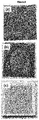
- FIG. 3 presents a typical cross-sectional morphology of the multi-layered structure inspected with scanning electron microscopy (SEM).
- SEM scanning electron microscopy
- FIG. 4 shows the x-ray diffraction (XRD) pattern of the (K,Na,Li)(Nb,Ta,Sb)O 3 ceramic layer obtained on the stainless steel (316L) plate.
- the layer exhibited a single phase of perovskite structure, without any secondary phase detected.
- the (K,Na,Li)(Nb,Ta,Sb)O 3 ceramic layer exhibited a high dielectric constant of 246 and a low dielectric loss of 1.8%, measured at 1 kHz and room temperature, as shown in FIG. 5 .
- the obtained (K,Na,Li)(Nb,Ta,Sb)O 3 ceramic layer was poled at 120° C. under an electric field of 35 kV/cm.
- the effective piezoelectric coefficient (d 33 ) was measured using a laser scanning vibrometer, under the condition with the substrate's mechanical clamping.
- FIG. 6 shows the three-dimensional drawing of the instantaneous vibration data of the (K,Na,Li)(Nb,Ta,Sb)O 3 layer under the electric sine wave driving.
- a unipolar AC signal of 20 V amplitude at 1 kHz was applied to the sample.
- the effective piezoelectric coefficient (d 33 ) was determined as 125 pm/V, under the substrate clamping effect.
- FIG. 7 ( a ) A multi-layered structure with the same substrate, piezoelectric ceramic and second electrode layers as Example 1, but without the first electrode layer, the metallic adhesive layer and the non-metallic thermal barrier layer, is schematically illustrated in FIG. 7 ( a ) .
- FIG. 7 ( b ) Another multi-layered structure with the layers as Example 1 but only without the intermediate layers, i.e. the metallic adhesive layer and the non-metallic thermal barrier layer is schematically shown in FIG. 7 ( b ) .
- the multi-layered structure as described in Example 1 exhibited structural integrity after heat treatment at 1100° C., as shown in FIG. 8 ( c ) .
- These results indicate the crucial role of the intermediate layer comprising the metallic adhesive layer and the non-metallic thermal barrier layer for enabling the feasibility of practical fabrication of a piezoelectric ceramic thick layer on a stainless steel substrate.
- the metallic adhesive layer provides oxidation and corrosion protection to the metal plate during the high-temperature thermal treatment in air as required for processing the piezoelectric ceramic thick layer
- the non-metallic thermal barrier layer acts as a thermal barrier layer to protect the metal plate from exposure to high temperature during the thermal spray process.
- FIG. 9 illustrates a cross-sectional view of a multi-layered structure according to a preferred embodiment, wherein the metal substrate is a stainless steel (316L) pipe.
- the multi-layered structure comprised a stainless steel (316L) pipe, a metallic adhesive layer made of NiCrAlY alloy, a non-metallic thermal barrier layer made of YSZ (ZrO 2 with 8 mol % Y 2 O 3 ), a first electrode layer comprising Pd/Ag, a lead-free piezoelectric ceramic layer with a composition of (K 0.44 Na 0.52 Li 0.04 )(Nb 0.84 Ta 0.10 Sb 0.06 )O 3 ((K,Na,Li)(Nb,Ta,Sb)O 3 ), and a second electrode layer comprising Ag.
- the multilayer structure was produced by a processing method as described in Example 1, but with different heat treatment conditions. It was found that the heat treatment conditions for the first electrode layer and the (K,Na,Li)(Nb,Ta,Sb)O 3 piezoelectric ceramic layer were critical in achieving the integrity for the multi-layered tube structure.
- the Pd/Ag (30/70) first electrode layer was heat-treated in an oven at a faster ramp rate of 100° C./min to a lower temperature of 950° C. for a shorter duration of 10 minutes.
- the heat treatment conditions as described above in this example achieved the structural integrity wherein the metal substrate was a stainless steel pipe.
- Using the same heat treatment conditions as described in Example 1 for a flat structured substrate resulted in failure in the multi-layered structure on the stainless pipe structure in the form of cracks and delamination.
- the (K,Na,Li)(Nb,Ta,Sb)O 3 layer was poled at room temperature for 10 minutes under an electric field of 30 kV/cm.
- the piezoelectric coefficient (d 33 ) was measured using a laser scanning vibrometer.
- FIG. 10 presents the three-dimensional drawing of the instantaneous vibration data of the (K,Na,Li)(Nb,Ta,Sb)O 3 ceramic layer produced on the stainless steel pipe structure under an electric sine wave driving, with 20 V amplitude at 1 kHz.
- the effective piezoelectric coefficient (d 33 ) was determined as 90 pm/V, under the substrate clamping effect.
- the multi-layered structure on the stainless steel pipe was produced by the same processing method as described in Example 3, except that the piezoelectric ceramic layer comprising (K,Na,Li)(Nb,Ta,Sb)O 3 was heat-treated by a flame from a butane blowtorch instead of thermal treatment in an oven.
- an electromagnetic irradiation such as laser, infrared
- a flame from any other fuel blowtorch may also be used.
- the heat treatment of the piezoelectric ceramic layer comprising (K,Na,Li)(Nb,Ta,Sb)O 3 was carried out for 8 minutes in air. The temperature reached 1102° C. The sample, after flame annealing for 8 minutes, exhibited solid structural integrity without cracking or delamination. Thus, fast annealing using flame blowtorch may produce the piezoelectric ceramic coating without cracking or delaminating on stainless steel pipe at least up to 1100° C.
- a Ag electrode was deposited on the piezoelectric ceramic layer comprising (K,Na,Li)(Nb,Ta,Sb)O 3 as the second electrode layer.
- the effective piezoelectric coefficient (d 33 ) was measured using a laser scanning vibrometer, under the conditions with the substrate's mechanical clamping.
- FIG. 11 shows a two-dimensional drawing of the instantaneous vibration data of the piezoelectric ceramic layer comprising (K,Na,Li)(Nb,Ta,Sb)O 3 under the electric sine wave driving, with a unipolar AC signal of 20 V at 1 kHz.
- the effective piezoelectric coefficient (d 33 ) was determined as 60 pm/V, under the substrate clamping effect.
Landscapes
- Engineering & Computer Science (AREA)
- Manufacturing & Machinery (AREA)
- Chemical & Material Sciences (AREA)
- Materials Engineering (AREA)
- Ceramic Engineering (AREA)
- Other Surface Treatments For Metallic Materials (AREA)
Abstract
Description
-
- a metal substrate;
- a metallic adhesive layer on a surface of the metal substrate;
- a non-metallic thermal barrier layer on the metallic adhesive layer; and
- a piezoelectric ceramic layer sandwiched between a first electrode layer and a second electrode layer, wherein the first electrode layer is on the non-metallic thermal barrier layer.
-
- providing a metal substrate;
- depositing a metallic adhesive layer on a surface of the metal substrate;
- depositing a non-metallic thermal barrier layer on the metallic adhesive layer;
- depositing a first electrode layer on the non-metallic thermal barrier layer;
- depositing a piezoelectric ceramic layer on the first electrode layer; and
- depositing a second electrode layer on the piezoelectric ceramic layer.
-
- a metal substrate;
- a metallic adhesive layer on a surface of the metal substrate;
- a non-metallic thermal barrier layer on the metallic adhesive layer; and
- a piezoelectric ceramic layer sandwiched between a first electrode layer and a second electrode layer, wherein the first electrode layer is on the non-metallic thermal barrier layer.
-
- providing a metal substrate;
- depositing a metallic adhesive layer on a surface of the metal substrate;
- depositing a non-metallic thermal barrier layer on the metallic adhesive layer;
- depositing a first electrode layer on the non-metallic thermal barrier layer;
- depositing a piezoelectric ceramic layer on the first electrode layer; and
- depositing a second electrode layer on the piezoelectric ceramic layer.
Claims (20)
Applications Claiming Priority (3)
| Application Number | Priority Date | Filing Date | Title |
|---|---|---|---|
| SG10201710100V | 2017-12-06 | ||
| SG10201710100V | 2017-12-06 | ||
| PCT/SG2018/050592 WO2019112518A1 (en) | 2017-12-06 | 2018-12-04 | A multi-layered piezoelectric ceramic-containing structure |
Publications (2)
| Publication Number | Publication Date |
|---|---|
| US20200388747A1 US20200388747A1 (en) | 2020-12-10 |
| US11527703B2 true US11527703B2 (en) | 2022-12-13 |
Family
ID=66749891
Family Applications (1)
| Application Number | Title | Priority Date | Filing Date |
|---|---|---|---|
| US16/769,120 Active 2039-10-03 US11527703B2 (en) | 2017-12-06 | 2018-12-04 | Multi-layered piezoelectric ceramic-containing structure |
Country Status (3)
| Country | Link |
|---|---|
| US (1) | US11527703B2 (en) |
| SG (1) | SG11202003158XA (en) |
| WO (1) | WO2019112518A1 (en) |
Citations (5)
| Publication number | Priority date | Publication date | Assignee | Title |
|---|---|---|---|---|
| US20050287386A1 (en) | 2002-09-23 | 2005-12-29 | Siemens Westinghouse Power Corporation | Method of instrumenting a component |
| JP2010118447A (en) | 2008-11-12 | 2010-05-27 | Nec Tokin Corp | Piezoelectric film type element |
| US20150044444A1 (en) * | 2012-04-23 | 2015-02-12 | The University Of Connecticut | Method of forming thermal barrier coating, thermal barrier coating formed thereby, and article comprising same |
| US20160133826A1 (en) | 2014-11-06 | 2016-05-12 | Agency For Science, Technology & Research | Method of making lead-free ceramic coating |
| US20170186936A1 (en) * | 2014-09-30 | 2017-06-29 | Fujifilm Corporation | Piezoelectric element production method thereof, actuator, and liquid discharge apparatus |
-
2018
- 2018-12-04 WO PCT/SG2018/050592 patent/WO2019112518A1/en not_active Ceased
- 2018-12-04 SG SG11202003158XA patent/SG11202003158XA/en unknown
- 2018-12-04 US US16/769,120 patent/US11527703B2/en active Active
Patent Citations (5)
| Publication number | Priority date | Publication date | Assignee | Title |
|---|---|---|---|---|
| US20050287386A1 (en) | 2002-09-23 | 2005-12-29 | Siemens Westinghouse Power Corporation | Method of instrumenting a component |
| JP2010118447A (en) | 2008-11-12 | 2010-05-27 | Nec Tokin Corp | Piezoelectric film type element |
| US20150044444A1 (en) * | 2012-04-23 | 2015-02-12 | The University Of Connecticut | Method of forming thermal barrier coating, thermal barrier coating formed thereby, and article comprising same |
| US20170186936A1 (en) * | 2014-09-30 | 2017-06-29 | Fujifilm Corporation | Piezoelectric element production method thereof, actuator, and liquid discharge apparatus |
| US20160133826A1 (en) | 2014-11-06 | 2016-05-12 | Agency For Science, Technology & Research | Method of making lead-free ceramic coating |
Non-Patent Citations (4)
| Title |
|---|
| Chen, S. et al., "Potassium sodium niobate (KNN)-based lead-free piezoelectric ceramic coatings on steel structure by thermal spray method", Journal of the American Ceramic Society, Jun. 4, 2018, vol. 101, No. 12, pp. 5524-5533 [Retrieved on Feb. 7, 2019] <DOI: 10.1111/JACE.15820>. |
| Derniaux, E. et al., "Effects of TiOx physical vapor deposition parameters on the preferred orientation and adhesion of Pt films on γ-Al203", Journal of Vacuum Science and Technology A, Jun. 23, 2006, vol. 24, No. 4, pp. 1540-1545 [Retrieved on Feb. 7, 2019] <DOI: 10.1116/1.2194925>. |
| International Preliminary Report on Patentability for International Application No. PCT/SG2018/050592 dated Jun. 9, 2020, 8 pages. |
| International Search Report and Written Opinion of the International Searching Authority issued in PCT/SG2018/050592, dated Feb. 8, 2019; ISA/SG. |
Also Published As
| Publication number | Publication date |
|---|---|
| US20200388747A1 (en) | 2020-12-10 |
| SG11202003158XA (en) | 2020-05-28 |
| WO2019112518A1 (en) | 2019-06-13 |
Similar Documents
| Publication | Publication Date | Title |
|---|---|---|
| Ghasemi et al. | Plasma-sprayed nanostructured YSZ thermal barrier coatings: thermal insulation capability and adhesion strength | |
| EP2754727A1 (en) | Novel architectures for ultra low thermal conductivity thermal barrier coatings with improved erosion and impact properties | |
| Choi et al. | Preparation and characterization of piezoelectric ceramic–polymer composite thick films by aerosol deposition for sensor application | |
| US10751756B2 (en) | Porosity control in piezoelectric films | |
| CN101204863A (en) | Thermal barrier coating system and method for coating components | |
| US6821656B2 (en) | Material for thermally loaded substrates | |
| Wu et al. | Thermal cycling behavior and bonding strength of single-ceramic-layer Sm2Zr2O7 and double-ceramic-layer Sm2Zr2O7/8YSZ thermal barrier coatings deposited by atmospheric plasma spraying | |
| JP2007254890A (en) | Method for forming strain-resistant coating by sol-gel method | |
| KR20210131150A (en) | Plasma resistance coating layer and forming method thereof | |
| US20110086177A1 (en) | Thermal spray method for producing vertically segmented thermal barrier coatings | |
| US20160133826A1 (en) | Method of making lead-free ceramic coating | |
| Sampath et al. | Plasma-spray forming ceramics and layered composites | |
| JP2015175315A (en) | Thermal barrier coating material, turbine member having the same, and thermal barrier coating method | |
| US9391258B2 (en) | Piezoelectric element | |
| US11527703B2 (en) | Multi-layered piezoelectric ceramic-containing structure | |
| JP6661269B2 (en) | Structure having coating film and method of manufacturing the same | |
| Lachowicz et al. | Corrosion damage mechanisms of TiO2 cold-sprayed coatings | |
| JP3876176B2 (en) | Ceramic composition for heat shielding coating film | |
| US6569546B1 (en) | Member with film formed by thermal spraying of thermal spray material | |
| Gao et al. | Tritium permeation barrier based on self-healing composite materials | |
| JP2009280854A (en) | Ceramic film and method of manufacturing the same and thermal barrier coating structure | |
| Ma et al. | Study of unique microstructure in SPS ceramic nanocoatings | |
| Krestou et al. | Fabrication of thin electrodic films by solution aerosol thermolysis (SAT) | |
| CN108707897A (en) | Exhaust pipe ceramic coating and preparation method thereof | |
| Thị et al. | Isothermal oxidation property of plasma sprayed 20YSZ/NiAl thermal barrier coating |
Legal Events
| Date | Code | Title | Description |
|---|---|---|---|
| FEPP | Fee payment procedure |
Free format text: ENTITY STATUS SET TO UNDISCOUNTED (ORIGINAL EVENT CODE: BIG.); ENTITY STATUS OF PATENT OWNER: LARGE ENTITY |
|
| AS | Assignment |
Owner name: AGENCY FOR SCIENCE, TECHNOLOGY AND RESEARCH, SINGAPORE Free format text: ASSIGNMENT OF ASSIGNORS INTEREST;ASSIGNORS:YAO, KUI;TAN, CHEE KIANG IVAN;CHEN, SHUTING;AND OTHERS;SIGNING DATES FROM 20190124 TO 20190130;REEL/FRAME:052998/0411 |
|
| STPP | Information on status: patent application and granting procedure in general |
Free format text: APPLICATION DISPATCHED FROM PREEXAM, NOT YET DOCKETED |
|
| STPP | Information on status: patent application and granting procedure in general |
Free format text: DOCKETED NEW CASE - READY FOR EXAMINATION |
|
| STPP | Information on status: patent application and granting procedure in general |
Free format text: NON FINAL ACTION MAILED |
|
| STPP | Information on status: patent application and granting procedure in general |
Free format text: RESPONSE TO NON-FINAL OFFICE ACTION ENTERED AND FORWARDED TO EXAMINER |
|
| STPP | Information on status: patent application and granting procedure in general |
Free format text: NOTICE OF ALLOWANCE MAILED -- APPLICATION RECEIVED IN OFFICE OF PUBLICATIONS |
|
| STPP | Information on status: patent application and granting procedure in general |
Free format text: NOTICE OF ALLOWANCE MAILED -- APPLICATION RECEIVED IN OFFICE OF PUBLICATIONS |
|
| STPP | Information on status: patent application and granting procedure in general |
Free format text: PUBLICATIONS -- ISSUE FEE PAYMENT VERIFIED |
|
| STCF | Information on status: patent grant |
Free format text: PATENTED CASE |