US11523080B2 - Photoelectric conversion device and electronic device with a ΔΣ A/D converter - Google Patents

Photoelectric conversion device and electronic device with a ΔΣ A/D converter Download PDF

Info

Publication number
US11523080B2
US11523080B2 US17/591,043 US202217591043A US11523080B2 US 11523080 B2 US11523080 B2 US 11523080B2 US 202217591043 A US202217591043 A US 202217591043A US 11523080 B2 US11523080 B2 US 11523080B2
Authority
US
United States
Prior art keywords
signal
converter
output
pixel
comparator
Prior art date
Legal status (The legal status is an assumption and is not a legal conclusion. Google has not performed a legal analysis and makes no representation as to the accuracy of the status listed.)
Active, expires
Application number
US17/591,043
Other versions
US20220247965A1 (en
Inventor
Daisuke Kobayashi
Current Assignee (The listed assignees may be inaccurate. Google has not performed a legal analysis and makes no representation or warranty as to the accuracy of the list.)
Canon Inc
Original Assignee
Canon Inc
Priority date (The priority date is an assumption and is not a legal conclusion. Google has not performed a legal analysis and makes no representation as to the accuracy of the date listed.)
Filing date
Publication date
Application filed by Canon Inc filed Critical Canon Inc
Assigned to CANON KABUSHIKI KAISHA reassignment CANON KABUSHIKI KAISHA ASSIGNMENT OF ASSIGNORS INTEREST (SEE DOCUMENT FOR DETAILS). Assignors: KOBAYASHI, DAISUKE
Publication of US20220247965A1 publication Critical patent/US20220247965A1/en
Application granted granted Critical
Publication of US11523080B2 publication Critical patent/US11523080B2/en
Active legal-status Critical Current
Adjusted expiration legal-status Critical

Links

Images

Classifications

    • H04N5/37455
    • HELECTRICITY
    • H03ELECTRONIC CIRCUITRY
    • H03MCODING; DECODING; CODE CONVERSION IN GENERAL
    • H03M3/00Conversion of analogue values to or from differential modulation
    • H03M3/30Delta-sigma modulation
    • H03M3/458Analogue/digital converters using delta-sigma modulation as an intermediate step
    • HELECTRICITY
    • H04ELECTRIC COMMUNICATION TECHNIQUE
    • H04NPICTORIAL COMMUNICATION, e.g. TELEVISION
    • H04N25/00Circuitry of solid-state image sensors [SSIS]; Control thereof
    • H04N25/70SSIS architectures; Circuits associated therewith
    • H04N25/76Addressed sensors, e.g. MOS or CMOS sensors
    • H04N25/77Pixel circuitry, e.g. memories, A/D converters, pixel amplifiers, shared circuits or shared components
    • H04N25/771Pixel circuitry, e.g. memories, A/D converters, pixel amplifiers, shared circuits or shared components comprising storage means other than floating diffusion
    • HELECTRICITY
    • H03ELECTRONIC CIRCUITRY
    • H03MCODING; DECODING; CODE CONVERSION IN GENERAL
    • H03M3/00Conversion of analogue values to or from differential modulation
    • H03M3/30Delta-sigma modulation
    • H03M3/39Structural details of delta-sigma modulators, e.g. incremental delta-sigma modulators
    • H03M3/412Structural details of delta-sigma modulators, e.g. incremental delta-sigma modulators characterised by the number of quantisers and their type and resolution
    • H03M3/422Structural details of delta-sigma modulators, e.g. incremental delta-sigma modulators characterised by the number of quantisers and their type and resolution having one quantiser only
    • H03M3/43Structural details of delta-sigma modulators, e.g. incremental delta-sigma modulators characterised by the number of quantisers and their type and resolution having one quantiser only the quantiser being a single bit one
    • HELECTRICITY
    • H03ELECTRONIC CIRCUITRY
    • H03MCODING; DECODING; CODE CONVERSION IN GENERAL
    • H03M3/00Conversion of analogue values to or from differential modulation
    • H03M3/30Delta-sigma modulation
    • H03M3/39Structural details of delta-sigma modulators, e.g. incremental delta-sigma modulators
    • H03M3/436Structural details of delta-sigma modulators, e.g. incremental delta-sigma modulators characterised by the order of the loop filter, e.g. error feedback type
    • H03M3/438Structural details of delta-sigma modulators, e.g. incremental delta-sigma modulators characterised by the order of the loop filter, e.g. error feedback type the modulator having a higher order loop filter in the feedforward path
    • H03M3/454Structural details of delta-sigma modulators, e.g. incremental delta-sigma modulators characterised by the order of the loop filter, e.g. error feedback type the modulator having a higher order loop filter in the feedforward path with distributed feedback, i.e. with feedback paths from the quantiser output to more than one filter stage
    • HELECTRICITY
    • H04ELECTRIC COMMUNICATION TECHNIQUE
    • H04NPICTORIAL COMMUNICATION, e.g. TELEVISION
    • H04N25/00Circuitry of solid-state image sensors [SSIS]; Control thereof
    • H04N25/70SSIS architectures; Circuits associated therewith
    • H04N25/76Addressed sensors, e.g. MOS or CMOS sensors
    • H04N25/78Readout circuits for addressed sensors, e.g. output amplifiers or A/D converters
    • H04N5/37452

Definitions

  • the present invention relates to a photoelectric conversion device and an electronic device.
  • ⁇ AD converter In the ⁇ AD converter disclosed in International Publication No. 2019/069614, the operation of a digital-to-analog (D/A) converter is controlled by a signal output from a quantizer (comparator).
  • a signal for controlling the D/A converter can be delayed due to a parasitic resistance or a parasitic capacitance in a wiring pattern from the comparator to the D/A converter. If a signal delay amount is changed because of a manufacturing variation or a change in the environment due to the temperature or the like, it may generate a conversion error in each ⁇ A/D converter or cause a variation in the operations of the ⁇ A/D converters among the columns and may degrade the accuracy of A/D conversion.
  • Some embodiments of the present invention provide a technique advantageous in improving the conversion accuracy of a delta-sigma analog-to-digital converter.
  • a photoelectric conversion device comprising a pixel unit in which a plurality of pixels each including a photoelectric conversion element are arranged in a matrix, and a signal processor configured to process a pixel signal output from the pixel unit via a vertical signal line
  • the signal processor comprises a ⁇ A/D converter configured to convert the pixel signal into a digital signal
  • the ⁇ A/D converter comprises a subtracter which includes a first input terminal to which the pixel signal is input and a second input terminal to which a subtraction signal is input, an integrator configured to receive an output from the subtracter, a comparator configured to compare an output from the integrator with a predetermined voltage, a decimation filter configured to generate the digital signal based on a comparison result output from the comparator, a delay unit configured to delay an output from the comparator, a buffer unit configured to buffer an output from the delay unit, and a D/A converter configured to convert an output from the buffer unit into an analog signal to generate the subtraction signal, is provided.
  • a photoelectric conversion device comprising a pixel unit in which a plurality of pixels each including a photoelectric conversion element are arranged in a matrix, and a signal processor configured to process a pixel signal output from the pixel unit via a vertical signal line
  • the signal processor comprises a conversion circuit configured to convert the pixel signal from a voltage signal into a current signal and a ⁇ A/D converter configured to convert the pixel signal, which has been converted into the current signal by the conversion circuit, into a digital signal
  • the ⁇ A/D converter includes a subtracter which comprises a first input terminal to which the pixel signal is input and a second input terminal to which a subtraction signal is input, an integrator configured to receive an output from the subtracter, a comparator configured to compare an output from the integrator with a predetermined voltage, a decimation filter configured to generate the digital signal based on a comparison result output from the comparator, a buffer unit configured to buffer an output from the comparator, and a D/A converter
  • FIG. 1 is a block diagram showing a schematic arrangement of a photoelectric conversion device according to an embodiment
  • FIG. 2 is a circuit diagram showing an example of the arrangement of a pixel of the photoelectric conversion device of FIG. 1 ;
  • FIGS. 3 A to 3 C are views each showing an example of the arrangement of a ⁇ A/D converter of the photoelectric conversion device of FIG. 1 ;
  • FIGS. 4 A and 4 B are views each showing an example of the arrangement of a buffer unit of the ⁇ A/D converter of the photoelectric conversion device of FIG. 1 ;
  • FIGS. 5 A and 5 B are views each showing an example of the arrangement of the ⁇ A/D converter of the photoelectric conversion device of FIG. 1 ;
  • FIG. 6 is a view showing an example of the arrangement of the ⁇ A/D converter of the photoelectric conversion device of FIG. 1 ;
  • FIGS. 7 A and 7 B are views each showing an example of the arrangement of the buffer unit of the ⁇ A/D converter of the photoelectric conversion device of FIG. 1 ;
  • FIG. 8 is a view showing an example of the arrangement of the ⁇ A/D converter of the photoelectric conversion device of FIG. 1 ;
  • FIGS. 9 A and 9 B are views each showing an example of the arrangement of a D/A converter of the ⁇ A/D converter of the photoelectric conversion device of FIG. 1 ;
  • FIGS. 10 A and 10 B are views each showing an example of the arrangement of the buffer unit of the ⁇ A/D converter of the photoelectric conversion device of FIG. 1 ;
  • FIG. 11 is a view showing an example of a current-to-voltage conversion circuit of the photoelectric conversion device of FIG. 1 ;
  • FIG. 12 is a block diagram showing an example of the arrangement of a camera incorporating the photoelectric conversion device according to the embodiment.
  • FIG. 1 is a block diagram showing an example of the arrangement of a photoelectric conversion device 100 according to an embodiment.
  • the photoelectric conversion device 100 includes a pixel unit 10 and a signal processor 600 which processes pixel signals output from the pixel unit 10 via corresponding vertical signal lines 12 .
  • the signal processor 600 includes a current supply unit 200 , a sample-and-hold unit 300 , an analog-to-digital (A/D) conversion unit 400 , a digital signal processor 500 , and an output unit 800 .
  • the photoelectric conversion device 100 may be a so-called CMOS image sensor.
  • a plurality of pixels 11 are arranged in a matrix. Assume here that a row direction indicates a horizontal direction in FIG. 1 , and a column direction indicates a vertical direction in FIG. 1 . Each pixel 11 generates a signal charge corresponding to incident light.
  • the vertical signal line 12 is arranged along the column direction in correspondence with each pixel column arranged with the pixels 11 .
  • the vertical signal lines 12 may be arranged so that a single vertical signal line will correspond to a single pixel column or so that a plurality of vertical signal lines will be arranged for a single pixel column.
  • Each vertical signal line 12 transfers, from each pixel 11 to the sample-and-hold unit 300 , a pixel signal corresponding to the signal charge generated by the photoelectric conversion element of the pixel 11 .
  • the current supply unit 200 is arranged in correspondence with the vertical signal lines 12 .
  • the current supply unit 200 supplies, via each vertical signal line 12 , a bias current to the corresponding pixel 11 selected for pixel signal readout.
  • the sample-and-hold unit 300 samples and holds, from the pixel unit 10 via the vertical signal line 12 , the signal generated by the photoelectric conversion element of each pixel 11 .
  • two sample-and-hold circuits which are a sample-and-hold circuit for sampling the signal when the photoelectric conversion element has been reset and a sample-and-hold circuit for sampling the signal when a photoelectric conversion operation has been performed in the photoelectric conversion element, can be connected to one vertical signal line 12 .
  • the A/D conversion unit 400 performs analog-to-digital conversion on each pixel signal input from the sample-and-hold unit 300 via a corresponding signal line 401 .
  • a delta-sigma ( ⁇ ) analog-to-digital (A/D) converter (to be also denoted as a ⁇ A/D converter hereinafter) that converts an analog pixel signal into a digital signal is connected in correspondence with each vertical signal line 12 .
  • the ⁇ A/D converter will be described later.
  • the digital signal processor 500 processes each digital signal output from the A/D conversion unit 400 via a corresponding signal line 501 .
  • the digital signal processor may perform correction processing, interpolation processing, or the like on each digital signal output from the A/D conversion unit 400 .
  • the output unit 800 outputs, from the photoelectric conversion device 100 to an external device, each signal processed by the digital signal processor 500 .
  • FIG. 2 is a circuit diagram showing an example of the arrangement of the pixel 11 .
  • the pixel 11 includes a photoelectric conversion element 13 , a transfer transistor 14 , a reset transistor 15 , an amplification transistor 16 , and a selection transistor 17 .
  • the photoelectric conversion element 13 can be, for example, a photodiode.
  • the photoelectric conversion element 13 has main electrodes, one of which is connected to a ground potential GND, photoelectrically converts received light into a signal charge of a charge amount corresponding to the amount of the received light, and accumulates the signal charge.
  • the other of the main electrodes of the photoelectric conversion element 13 is electrically connected to the gate electrode of the amplification transistor 16 via the transfer transistor 14 .
  • Anode FD to which the gate electrode of the amplification transistor 16 is electrically connected, functions as a floating diffusion.
  • the node FD which functions as the floating diffusion is a charge-to-voltage conversion unit that converts the signal charge generated by the photoelectric conversion element 13 into a signal voltage.
  • a transfer signal PTX is supplied to the gate electrode of the transfer transistor 14 .
  • the transfer transistor 14 is set in a conductive state in accordance with the transfer signal PTX, photoelectric conversion is executed in the photoelectric conversion element 13 , and the signal charge accumulated in the photoelectric conversion element 13 is transferred to the node FD which functions as a floating diffusion.
  • the reset transistor 15 is connected between a power supply potential VDD and the node FD.
  • the expression here that “a transistor is connected between A and B” represents a state in which one of the main electrodes of the transistor is connected to A and the other of the main electrodes is connected to B.
  • the gate electrode of the transistor is connected to neither A nor B.
  • a reset signal PRES is supplied to the gate electrode of the reset transistor 15 .
  • the reset transistor 15 is set in a conductive state in accordance with the reset signal PRES, the potential of the node FD (floating diffusion) is reset to the power supply potential VDD, and the charge accumulated in the floating diffusion is swept out.
  • the amplification transistor 16 is connected between the power supply potential VDD and the selection transistor 17 , and the gate electrode of the amplification transistor 16 is connected to the node FD.
  • the amplification transistor 16 is an input unit of a source follower which reads out the signal obtained from the photoelectric conversion by the photoelectric conversion element 13 . That is, the other of the main electrodes of the amplification transistor 16 is connected to the vertical signal line 12 via the selection transistor 17 .
  • the amplification transistor 16 and the above-described current supply unit 200 connected to the vertical signal line 12 form a source follower which converts the voltage of the node FD into a potential of the vertical signal line 12 .
  • the selection transistor 17 is connected between the amplification transistor 16 and the vertical signal line 12 .
  • a selection signal PSEL is supplied to the gate electrode of the selection transistor 17 .
  • the selection transistor 17 is set in a conductive state in accordance with the selection signal PSEL, the pixel 11 is set in a selected state, and a signal output from the amplification transistor 16 is transmitted to the vertical signal line 12 .
  • the circuit arrangement of the pixel 11 is not limited to the arrangement shown in FIG. 2 .
  • the selection transistor 17 may be connected between the power supply potential VDD and the amplification transistor 16 .
  • the arrangement shown in FIG. 2 shows, as the pixel 11 , a so-called four-transistor arrangement including the transfer transistor 14 , the reset transistor 15 , the amplification transistor 16 , and the selection transistor 17 , the present invention is not limited to this.
  • the pixel 11 may have a three-transistor arrangement in which the selection transistor 17 is omitted and the amplification transistor 16 also functions as a selection transistor.
  • an arrangement with an increased number of transistors such as an arrangement having five transistors or more may be used as the pixel 11 .
  • the ⁇ A/D converter 450 that is arranged in the A/D conversion unit 400 and converts the pixel signal into a digital signal will be described next with reference to FIG. 3 A .
  • the ⁇ A/D converter 450 includes a subtracter 45 , an integrator 40 , a comparator 41 (to be also referred to as a quantizer), a digital-to-analog (D/A) converter 44 , and a decimation filter 43 .
  • the subtracter 45 includes an input (+) terminal to which a pixel signal from the sample-and-hold unit 300 is input via the signal line 401 and an input ( ⁇ ) terminal to which a subtraction signal is input.
  • the integrator 40 receives an output from the subtracter 45 and outputs an integrated value to the comparator 41 via a signal line 405 .
  • the comparator 41 compares the output from the integrator 40 with a predetermined voltage. If a signal output as a comparison result from the comparator 41 is 1 bit, the predetermined voltage can be one kind of voltage. If the output from the comparator 41 is 2 bits or more, the comparator 41 will output a comparison result obtained by comparing the output from the integrator 40 with a plurality of kinds of voltages.
  • the decimation filter 43 generates a digital signal based on the comparison result output from the comparator 41 via a signal line 42 , and outputs the generated digital signal to the digital signal processor 500 via the signal line 501 .
  • the D/A converter 44 converts the output from the comparator 41 via the vertical signal line 12 into an analog signal, and generates the subtraction signal to be output to the input ( ⁇ ) terminal of the subtracter 45 .
  • the subtracter 45 obtains a difference between the pixel signal supplied to the input (+) terminal and the subtraction signal supplied to the input ( ⁇ ) terminal to feed back a previously sampled data value to the pixel signal, thereby reducing the quantization noise.
  • a signal line 20 can be the ground potential GND.
  • the ⁇ A/D converter 450 includes a delay unit 46 that delays the signal of the comparison result output from the comparator 41 .
  • a signal to be input to the ⁇ A/D converter 450 can also be delayed in the integrator 40 or the comparator 41 .
  • a delay can also occur due to a parasitic load or the like in the signal line 405 or 42 in the ⁇ A/D converter 450 .
  • the delay unit 46 represents a delay component in a circuit or a signal line in the ⁇ A/D converter 450 .
  • the ⁇ A/D converter 450 may not include some kind of element as the delay unit 46 .
  • the D/A converter 44 is controlled by the output (comparison result) from the comparator 41 .
  • the output from the comparator 41 for controlling the D/A converter 44 can be delayed due to a parasitic resistance or a parasitic capacitance in the wiring pattern of the signal line 42 from the comparator 41 to the D/A converter 44 .
  • the signal line 42 is laid out to extend in a single direction like a column circuit, the influence of the parasitic load of the signal line 42 will increase, and the signal will be delayed.
  • the delay amount of this delay may change depending on a manufacturing variation in the photoelectric conversion device 100 or a change in the environment due to the temperature or the like.
  • the variation or the change in the delay amount can generate a conversion error in the ⁇ A/D converter 450 or cause operational variation among the ⁇ A/D converters 450 arranged in correspondence with the vertical signal lines 12 . As a result, it may degrade the image quality of an image obtained by the photoelectric conversion device 100 .
  • a buffer unit 411 that buffers a signal, which is output from the comparator 41 and is input to the D/A converter 44 via the signal line 42 , is arranged between the comparator 41 and the D/A converter 44 .
  • the control by the D/A converter 44 influences the accuracy of the A/D conversion by the ⁇ A/D converter 450 .
  • a delay amount variation among the columns corresponding to the vertical signal lines 12 can also be reduced by arranging the buffer unit 411 , thus reducing an A/D conversion variation among the columns.
  • the buffer unit 411 can include an amplifier 423 which is formed by two stages of inverter circuits 420 . Since the buffer unit 411 buffers the output of the comparator 41 , the output from the comparator 41 (the output from the delay unit 46 ) is amplified and undergoes waveform shaping, impedance conversion, and the like. As a result, the accuracy of the A/D conversion is improved.
  • the buffer unit 411 can include a level shifter 424 to convert the level of the output from the comparator 41 .
  • the voltage of signal can be increased or decreased in the buffer unit 411 to allow the D/A converter 44 to operate appropriately.
  • the circuit arrangement of the amplifier 423 and that of the level shifter 424 are not limited to those shown in FIGS. 4 A and 4 B , respectively, and a circuit having an appropriate arrangement can be used.
  • FIG. 3 A shows a case in which a voltage signal is input as a pixel signal via the signal line 401 .
  • FIG. 3 B shows a case in which a current signal is input as a pixel signal to the ⁇ A/D converter 450 .
  • the signal processor 600 will need to convert the pixel signal from a voltage signal into a current signal because a signal output from the pixel 11 is a voltage signal as described above.
  • the signal processor 600 further includes a conversion circuit that converts the pixel signal from a voltage signal into a current signal.
  • the sample-and-hold unit 300 may be arranged to include a conversion circuit so that a signal output from the sample-and-hold unit 300 will be a current signal.
  • a conversion circuit 47 that converts a voltage signal into a current signal may be arranged between the sample-and-hold unit 300 and the ⁇ A/D converter 450 .
  • a pixel signal that has been converted into a current signal can be input to the subtracter 45 by such arrangement. Note that as described above, since the delay unit 46 represents a delay component in the circuit or a signal line in the ⁇ A/D converter 450 and there may be a case in which no element is included as the delay unit 46 , the delay unit 46 is not illustrated in FIG. 3 B and drawings thereafter.
  • FIG. 3 C shows an example of a more specific arrangement of the ⁇ A/D converter 450 in which a pixel signal that has been converted into a current signal is input.
  • a capacitive element 402 is arranged as the above-described integrator 40 .
  • a D/A converter 403 is arranged as the above-described D/A converter 44 .
  • the capacitive element 402 is connected in parallel to the D/A converter 403 .
  • the D/A converter 403 can include a current supply source for supplying a current to the signal line 405 .
  • this change (for example, the change between supplying and not supplying of the current) in the current amount supplied to the signal line 405 by the D/A converter 403 in accordance with the output (comparison result) from the comparator 41 corresponds to the operation of the subtracter 45 described above.
  • the ⁇ A/D converter arranged in the A/D conversion unit 400 is not limited to an arrangement that performs first-order ⁇ modulation in the manner of the ⁇ A/D converter 450 shown in FIGS. 3 A to 3 C .
  • a ⁇ A/D converter 451 that performs second-order ⁇ modulation may be arranged in the A/D conversion unit 400 .
  • the subtracter 45 , the integrator 40 , and the D/A converter 44 shown in FIG. 3 A are set as a subtracter 45 a , an integrator 40 a , and a D/A converter 44 a , respectively.
  • the ⁇ A/D converter 451 further includes an integrator 40 b , a subtracter 45 b , and a D/A converter 44 b .
  • the integrator 40 b is connected between the integrator 40 a and the comparator 41 .
  • the subtracter 45 b includes an input (+) terminal which receives the output from the integrator 40 a and an input ( ⁇ ) terminal to which a subtraction signal from the D/A converter 44 b is input.
  • the subtracter 45 b outputs a subtraction result to the integrator 40 b .
  • a buffer unit 411 a is arranged between the comparator 41 and the D/A converter 44 a
  • a buffer unit 411 b is arranged between the comparator 41 and the D/A converter 44 b .
  • the D/A converter 44 b converts the output from the buffer unit 411 b into an analog signal and generates the subtraction signal to be supplied to the subtracter 45 b.
  • the buffer units 411 a and 411 b perform the role of impedance transformation to relay the conversion result output by the comparator 41 . This will reduce the blunting of the waveform of the signal indicating the comparison result. Also, the addition of a delay amount will reduce the influence of the variation in the delay amount, thereby suppressing the degradation of the accuracy of the A/D conversion.
  • the buffer units 411 a and 411 b may include, for example, the amplifier 423 as shown in FIG. 4 A .
  • the accuracy of the A/D conversion can be further improved by causing the ⁇ A/D converter 451 to perform second-order ⁇ modulation.
  • a ⁇ A/D converter that has an arrangement to perform higher-order ⁇ modulation such as ⁇ modulation with an order of 3 or higher may be arranged in the A/D conversion unit 400 .
  • the two buffer units 411 a and 411 b may be arranged as the buffer units as shown in FIG. 5 A
  • the present invention is not limited to this.
  • only the buffer unit 411 b may be arranged in the ⁇ A/D converter 451 .
  • the output from the comparator 41 which is to be supplied to the D/A converter 44 a and the D/A converter 44 b can be buffered.
  • only the buffer unit 411 a may be arranged in the ⁇ A/D converter 451 .
  • the influence from the parasitic load of the signal line 42 can be greater.
  • the buffer unit 411 a will be arranged between the output terminal of the comparator 41 and the input terminal of the D/A converter 44 a , a buffered signal will be supplied to the D/A converter 44 a , and no buffer unit will be arranged between the output terminal of the comparator 41 and the input terminal of the D/A converter 44 b .
  • FIG. 5 B is a view showing an example of the arrangement for performing second-order ⁇ modulation when a pixel signal which has been converted into a current signal is to be input to the ⁇ A/D converter 451 .
  • Two sets of the capacitive element 402 and the D/A converter 403 are arranged.
  • a capacitive element 402 a functions as the integrator 40 a of FIG. 5 A
  • a D/A converter 403 a functions as the subtracter 45 a and the D/A converter 44 a of FIG. 5 A .
  • a capacitive element 402 b functions as the integrator 40 b of FIG.
  • a D/A converter 403 b functions as the subtracter 45 b and the D/A converter 44 b of FIG. 5 A .
  • the capacitive element 402 b is connected in parallel to the D/A converter 403 b .
  • a current-to-voltage conversion circuit 48 is arranged between the two sets of the capacitive element and the D/A converter.
  • a gm amplifier for example, as shown in FIG. 11 may be used for the current-to-voltage conversion circuit 48 .
  • Conversion circuits which have the same arrangement or circuits which have different arrangements may be used for the current-to-voltage conversion circuit 48 and the conversion circuit 47 for supplying a current signal to the ⁇ A/D converter 451 . It is sufficient as long as appropriate circuits are used in accordance with the respective specifications of the conversion circuit 47 and the current-to-voltage conversion circuit 48 .
  • FIG. 5 B A modification of the ⁇ A/D converter 451 shown in FIG. 5 B will be described next with reference to FIGS. 6 , 7 A, and 7 B .
  • the output from the buffer unit 411 b is supplied to the buffer unit 411 a and the D/A converter 403 b via a common signal line 480 .
  • the output from the buffer unit 411 b is supplied to the buffer unit 411 a via the signal line 480 and supplied to D/A converter 403 b via a signal line 482 which is separate from the signal line 480 .
  • FIGS. 7 A and 7 B show the arrangement example of the buffer unit 411 a and the arrangement example of the buffer unit 411 b , respectively.
  • the buffer units 411 a and 411 b each include a phase adjuster 421 as shown in FIGS. 7 A and 7 B . This allows each of the buffer units 411 a and 411 b to perform phase adjustment on the output from the comparator 41 .
  • Phase adjustment may be performed on both the signal supplied to the D/A converter 403 a and the signal supplied to the D/A converter 403 b or may be performed on one of the signal supplied to the D/A converter 403 a and the signal supplied to the D/A converter 403 b .
  • the combination to be used to execute phase adjustment can be switched by appropriately selecting switches S 0 to S 3 shown in FIGS. 7 A and 7 B to set a conductive state or a non-conductive state. At this time, control may be performed so that the phase relationship between the phase of the output from the comparator 41 for controlling the D/A converter 403 a and the phase of the output from the comparator 41 for controlling the D/A converter 403 b will constantly have the same relationship.
  • the phase of a signal supplied via a signal line 481 to the D/A converter 403 a on the upstream side with respect to the input of a pixel signal may occur ahead of the phase of a signal supplied to the D/A converter 403 b via the signal line 482 .
  • the present invention is not limited to this, and the phase of the signal supplied to the D/A converter 403 a may lag behind the phase of the signal supplied to the D/A converter 403 b .
  • the phase relationship can be appropriately set to improve the accuracy of the A/D conversion or to suppress the variation among the columns corresponding to the vertical signal lines 12 .
  • the phase of an output signal from the comparator 41 supplied to the D/A converter 403 b which was occurring ahead of the phase of an output signal supplied to the D/A converter 403 a may lag due to a change in the parasitic load amount caused by an environmental change, and the phase of the output signal supplied to the D/A converter 403 a may occur ahead during an operation. If the phase (timing) of the signal output from the comparator 41 to each of the D/A converters 403 a and 403 b changes, the results of the A/D conversion may increasingly vary. Hence, it will be possible to improve the accuracy of the A/D conversion by providing a phase adjustment function to each of the buffer units 411 a and 411 b.
  • the buffer unit 411 may perform phase adjustment on the output from the comparator 41 even in the ⁇ A/D converter 450 which performs first-order ⁇ modulation and is shown in FIGS. 3 A to 3 C .
  • the accuracy of the A/D conversion can be improved by adjusting the phase so that each signal output from the comparator 41 and supplied to the D/A converters 44 and 403 will have an appropriate delay amount.
  • the level shifter 424 and the amplifier 423 using the inverter circuit 420 or the like may be arranged in each of the buffer units 411 a and 411 b .
  • the buffer units 411 a and 411 b can appropriately combine and perform amplification, level conversion, and phase adjustment on the output from the comparator 41 .
  • the signal output from the comparator 41 may be buffered by combining one or a plurality of the amplification, level conversion, and phase adjustment operations by arranging so that each of the buffer units 411 a and 411 b will have a plurality of paths which are switchable by a switch.
  • different buffering processes may be performed by the buffer units 411 a and 411 b.
  • FIG. 8 is a view showing an example of the arrangement of a ⁇ A/D converter 453 which performs A/D conversion on a pixel signal converted into a current signal.
  • a pixel signal supplied via the signal line 401 may have a wide dynamic range in accordance with the increase in the dynamic range of the photoelectric conversion device 100 .
  • an analog switch In order to perform A/D conversion on a pixel signal which has a wide dynamic range without losing the signal range, an analog switch will be used as a switch to supply a current from a current supply source arranged in each of the D/A converters 403 a and 403 b to a corresponding one of signal lines 405 a and 405 b.
  • FIGS. 9 A and 9 B are views showing an example of the arrangement of the D/A converters 403 a and 403 b , respectively.
  • each of the D/A converters 403 a and 403 b includes a current supply source 472 and an analog switch 471 (CMOS analog switch) for controlling the supply of current from the current supply source 472 to the corresponding one of the signal lines 405 a and 405 b.
  • CMOS analog switch CMOS analog switch
  • FIGS. 10 A and 10 B are views showing an example of the arrangement of the buffer units 411 a and 411 b , respectively, for supplying the signal output from the comparator 41 to the D/A converters 403 a and 403 b .
  • each of the buffer units 411 a and 411 b will buffer the output from the comparator 41 to generate a non-inverting signal and an inverting signal in correspondence with the comparison result output from the comparator 41 .
  • the analog switch 471 will operate in accordance with the non-inverting signal and the inverting signal.
  • each of the buffer units 411 a and 411 b includes the inverter circuits 420 and a non-inverting amplification circuit 422 .
  • the buffer unit 411 a for each comparison result signal output from the comparator 41 and received via the signal line 42 , a non-inverting signal to be output to the signal line 481 via the inverter circuits 420 and an inverting signal to be output to a signal line 483 via the inverter circuit 420 and the non-inverting amplification circuit 422 are generated. As shown in FIG.
  • the non-inverting signal and the inverting signal are supplied via the signal lines 481 and 483 , respectively, from the buffer unit 411 a to the D/A converter 403 a .
  • a non-inverting signal to be output to the signal line 480 via the inverter circuits 420 and an inverting signal to be output to the signal line 482 via the inverter circuit 420 and the non-inverting amplification circuit 422 are generated.
  • the non-inverting signal and the inverting signal are supplied via the signal lines 480 and 482 , respectively, from the buffer unit 411 b to the D/A converter 403 b.
  • the non-inverting signals and the inverting signals with aligning phases are generated by the buffer units 411 a and 411 b based on the comparison result signal as a control signal output from the comparator 41 , and the generated signals are supplied to the D/A converters 403 a and 403 b .
  • the analog switch 471 arranged in each of the D/A converters 403 a and 403 b can be appropriately controlled.
  • level conversion processing may be performed by arranging the above-described level shifter 424 in each of the buffer units 411 a and 411 b shown in FIGS. 10 A and 10 B . This is for a case in which the operation voltage of the comparator 41 differs from the operation voltages of the signal lines 405 a and 405 b generated by the capacitive elements 402 a and 402 b functioning as the integrator 40 .
  • phase adjustment may be performed in a manner similar to that as described above by arranging the phase adjuster 421 in each of the buffer units 411 a and 411 b.
  • FIG. 12 is a schematic view of an electronic device EQP incorporating the photoelectric conversion device 100 .
  • FIG. 12 shows a camera as an example of the electronic device EQP.
  • the concept of a camera here not only includes an apparatus whose main object is image capturing, but also an apparatus (for example, a personal computer or a mobile terminal such as a smartphone) that has an image capturing function auxiliary.
  • the photoelectric conversion device 100 can be a semiconductor chip with a stacked structure including the pixel unit 10 . As shown in FIG. 12 , the photoelectric conversion device 100 is contained in a semiconductor package PKG.
  • the semiconductor package PKG can include a base to which the photoelectric conversion device 100 is fixed, a lid such as glass facing the photoelectric conversion device 100 , and a conductive connecting member such as a bonding wire or bump used to connect the terminal arranged in the base to a terminal arranged in the photoelectric conversion device 100 .
  • the device EQP may further include at least one of an optical system OPT, a control device CTRL, a processing device PRCS, a display device DSPL, and a storage device MMRY.
  • the optical system OPT is a system for forming an image on the pixel unit 10 of the photoelectric conversion device 100 , and can be, for example, a lens, a shutter, and a mirror.
  • the control device CTRL is a device for controlling the operation of the photoelectric conversion device 100 , and can be, for example, a semiconductor device such as an ASIC or the like.
  • the processing device PRCS is a device for processing the signal output from the photoelectric conversion device 100 , and can be, for example, a semiconductor device such as a CPU, an ASIC, or the like.
  • the display device DSPL can be an EL display device or a liquid crystal display device that displays image data obtained by the photoelectric conversion device 100 .
  • the storage device MMRY is a magnetic device or a semiconductor device for storing the image data obtained by the photoelectric conversion device 100 .
  • the storage device MMRY can be a volatile memory such as SRAM, DRAM, or the like or a nonvolatile memory such as a flash memory or a hard disk drive.
  • a mechanical device MCHN includes a driving unit or propulsion unit such as a motor, an engine, or the like.
  • the mechanical device MCHN in the camera can drive the components of the optical system OPT for zooming, focusing, and shutter operations.
  • image data output from the photoelectric conversion device 100 is displayed on the display DSPL and is transmitted to an external device by a communication device (not shown) included in the equipment EQP.
  • the equipment EQP may also include the storage device MMRY and the processing device PRCS as shown in FIG. 12 .
  • the camera incorporating the photoelectric conversion device 100 is applicable as a monitoring camera or an onboard camera mounted in a transportation equipment such as an automobile, a railroad car, a ship, an airplane, an industrial robot, or the like.
  • the camera incorporating the photoelectric conversion device 100 is not limited to a transportation equipment but is also applicable to a device that widely uses object recognition such as an intelligent transportation system (ITS).
  • ITS intelligent transportation system

Landscapes

  • Engineering & Computer Science (AREA)
  • Theoretical Computer Science (AREA)
  • Multimedia (AREA)
  • Signal Processing (AREA)
  • Transforming Light Signals Into Electric Signals (AREA)
  • Analogue/Digital Conversion (AREA)
  • Compression, Expansion, Code Conversion, And Decoders (AREA)

Abstract

A photoelectric converter comprising a pixel unit and a processor configured to process a pixel signal output from the pixel unit is provided. The processor comprises a ΔΣ AD converter configured to convert the pixel signal into a digital signal. The ΔΣ AD converter comprises a subtracter to which the pixel signal and a subtraction signal are input, an integrator configured to receive an output from the subtracter, a comparator configured to compare an output from the integrator with a predetermined voltage, a decimation filter configured to generate the digital signal based on an output from the comparator, a delay unit configured to delay an output from the comparator, a buffer configured to buffer an output from the delay unit, and a DA converter configured to convert an output from the buffer into an analog signal to generate the subtraction signal.

Description

BACKGROUND OF THE INVENTION Field of the Invention
The present invention relates to a photoelectric conversion device and an electronic device.
Description of the Related Art
International Publication No. 2019/069614 discloses a solid-state image capturing apparatus that uses a delta-sigma (ΔΣ) analog-to-digital (A/D) converter in an analog-to-digital conversion unit.
SUMMARY OF THE INVENTION
In the ΔΣ AD converter disclosed in International Publication No. 2019/069614, the operation of a digital-to-analog (D/A) converter is controlled by a signal output from a quantizer (comparator). A signal for controlling the D/A converter can be delayed due to a parasitic resistance or a parasitic capacitance in a wiring pattern from the comparator to the D/A converter. If a signal delay amount is changed because of a manufacturing variation or a change in the environment due to the temperature or the like, it may generate a conversion error in each ΔΣ A/D converter or cause a variation in the operations of the ΔΣ A/D converters among the columns and may degrade the accuracy of A/D conversion.
Some embodiments of the present invention provide a technique advantageous in improving the conversion accuracy of a delta-sigma analog-to-digital converter.
According to some embodiments, a photoelectric conversion device comprising a pixel unit in which a plurality of pixels each including a photoelectric conversion element are arranged in a matrix, and a signal processor configured to process a pixel signal output from the pixel unit via a vertical signal line, wherein the signal processor comprises a ΔΣ A/D converter configured to convert the pixel signal into a digital signal, the ΔΣ A/D converter comprises a subtracter which includes a first input terminal to which the pixel signal is input and a second input terminal to which a subtraction signal is input, an integrator configured to receive an output from the subtracter, a comparator configured to compare an output from the integrator with a predetermined voltage, a decimation filter configured to generate the digital signal based on a comparison result output from the comparator, a delay unit configured to delay an output from the comparator, a buffer unit configured to buffer an output from the delay unit, and a D/A converter configured to convert an output from the buffer unit into an analog signal to generate the subtraction signal, is provided.
According to some other embodiments, a photoelectric conversion device comprising a pixel unit in which a plurality of pixels each including a photoelectric conversion element are arranged in a matrix, and a signal processor configured to process a pixel signal output from the pixel unit via a vertical signal line, wherein the signal processor comprises a conversion circuit configured to convert the pixel signal from a voltage signal into a current signal and a ΔΣ A/D converter configured to convert the pixel signal, which has been converted into the current signal by the conversion circuit, into a digital signal, the ΔΣ A/D converter includes a subtracter which comprises a first input terminal to which the pixel signal is input and a second input terminal to which a subtraction signal is input, an integrator configured to receive an output from the subtracter, a comparator configured to compare an output from the integrator with a predetermined voltage, a decimation filter configured to generate the digital signal based on a comparison result output from the comparator, a buffer unit configured to buffer an output from the comparator, and a D/A converter configured to convert an output from the buffer unit into an analog signal to generate the subtraction signal, is provided.
Further features of the present invention will become apparent from the following description of exemplary embodiments (with reference to the attached drawings).
BRIEF DESCRIPTION OF THE DRAWINGS
FIG. 1 is a block diagram showing a schematic arrangement of a photoelectric conversion device according to an embodiment;
FIG. 2 is a circuit diagram showing an example of the arrangement of a pixel of the photoelectric conversion device of FIG. 1 ;
FIGS. 3A to 3C are views each showing an example of the arrangement of a ΔΣ A/D converter of the photoelectric conversion device of FIG. 1 ;
FIGS. 4A and 4B are views each showing an example of the arrangement of a buffer unit of the ΔΣ A/D converter of the photoelectric conversion device of FIG. 1 ;
FIGS. 5A and 5B are views each showing an example of the arrangement of the ΔΣ A/D converter of the photoelectric conversion device of FIG. 1 ;
FIG. 6 is a view showing an example of the arrangement of the ΔΣ A/D converter of the photoelectric conversion device of FIG. 1 ;
FIGS. 7A and 7B are views each showing an example of the arrangement of the buffer unit of the ΔΣ A/D converter of the photoelectric conversion device of FIG. 1 ;
FIG. 8 is a view showing an example of the arrangement of the ΔΣ A/D converter of the photoelectric conversion device of FIG. 1 ;
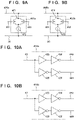
FIGS. 9A and 9B are views each showing an example of the arrangement of a D/A converter of the ΔΣ A/D converter of the photoelectric conversion device of FIG. 1 ;
FIGS. 10A and 10B are views each showing an example of the arrangement of the buffer unit of the ΔΣ A/D converter of the photoelectric conversion device of FIG. 1 ;
FIG. 11 is a view showing an example of a current-to-voltage conversion circuit of the photoelectric conversion device of FIG. 1 ; and
FIG. 12 is a block diagram showing an example of the arrangement of a camera incorporating the photoelectric conversion device according to the embodiment.
DESCRIPTION OF THE EMBODIMENTS
Hereinafter, embodiments will be described in detail with reference to the attached drawings. Note, the following embodiments are not intended to limit the scope of the claimed invention. Multiple features are described in the embodiments, but limitation is not made to an invention that requires all such features, and multiple such features may be combined as appropriate. Furthermore, in the attached drawings, the same reference numerals are given to the same or similar configurations, and redundant description thereof is omitted.
A photoelectric conversion device according to an embodiment of the present invention will be described with reference to FIGS. 1 to 12 . FIG. 1 is a block diagram showing an example of the arrangement of a photoelectric conversion device 100 according to an embodiment. The photoelectric conversion device 100 includes a pixel unit 10 and a signal processor 600 which processes pixel signals output from the pixel unit 10 via corresponding vertical signal lines 12. The signal processor 600 includes a current supply unit 200, a sample-and-hold unit 300, an analog-to-digital (A/D) conversion unit 400, a digital signal processor 500, and an output unit 800. The photoelectric conversion device 100 may be a so-called CMOS image sensor.
In the pixel unit 10, a plurality of pixels 11, each including a photoelectric conversion element, are arranged in a matrix. Assume here that a row direction indicates a horizontal direction in FIG. 1 , and a column direction indicates a vertical direction in FIG. 1 . Each pixel 11 generates a signal charge corresponding to incident light.
In the pixel unit 10, the vertical signal line 12 is arranged along the column direction in correspondence with each pixel column arranged with the pixels 11. The vertical signal lines 12 may be arranged so that a single vertical signal line will correspond to a single pixel column or so that a plurality of vertical signal lines will be arranged for a single pixel column. Each vertical signal line 12 transfers, from each pixel 11 to the sample-and-hold unit 300, a pixel signal corresponding to the signal charge generated by the photoelectric conversion element of the pixel 11.
The current supply unit 200 is arranged in correspondence with the vertical signal lines 12. The current supply unit 200 supplies, via each vertical signal line 12, a bias current to the corresponding pixel 11 selected for pixel signal readout.
The sample-and-hold unit 300 samples and holds, from the pixel unit 10 via the vertical signal line 12, the signal generated by the photoelectric conversion element of each pixel 11. For example, in the sample-and-hold unit 300, two sample-and-hold circuits, which are a sample-and-hold circuit for sampling the signal when the photoelectric conversion element has been reset and a sample-and-hold circuit for sampling the signal when a photoelectric conversion operation has been performed in the photoelectric conversion element, can be connected to one vertical signal line 12.
The A/D conversion unit 400 performs analog-to-digital conversion on each pixel signal input from the sample-and-hold unit 300 via a corresponding signal line 401. In the A/D conversion unit, a delta-sigma (ΔΣ) analog-to-digital (A/D) converter (to be also denoted as a ΔΣ A/D converter hereinafter) that converts an analog pixel signal into a digital signal is connected in correspondence with each vertical signal line 12. The ΔΣ A/D converter will be described later.
The digital signal processor 500 processes each digital signal output from the A/D conversion unit 400 via a corresponding signal line 501. For example, the digital signal processor may perform correction processing, interpolation processing, or the like on each digital signal output from the A/D conversion unit 400. The output unit 800 outputs, from the photoelectric conversion device 100 to an external device, each signal processed by the digital signal processor 500.
FIG. 2 is a circuit diagram showing an example of the arrangement of the pixel 11. The pixel 11 includes a photoelectric conversion element 13, a transfer transistor 14, a reset transistor 15, an amplification transistor 16, and a selection transistor 17. The photoelectric conversion element 13 can be, for example, a photodiode. The photoelectric conversion element 13 has main electrodes, one of which is connected to a ground potential GND, photoelectrically converts received light into a signal charge of a charge amount corresponding to the amount of the received light, and accumulates the signal charge. The other of the main electrodes of the photoelectric conversion element 13 is electrically connected to the gate electrode of the amplification transistor 16 via the transfer transistor 14. Anode FD, to which the gate electrode of the amplification transistor 16 is electrically connected, functions as a floating diffusion. The node FD which functions as the floating diffusion is a charge-to-voltage conversion unit that converts the signal charge generated by the photoelectric conversion element 13 into a signal voltage.
A transfer signal PTX is supplied to the gate electrode of the transfer transistor 14. When the transfer transistor 14 is set in a conductive state in accordance with the transfer signal PTX, photoelectric conversion is executed in the photoelectric conversion element 13, and the signal charge accumulated in the photoelectric conversion element 13 is transferred to the node FD which functions as a floating diffusion.
The reset transistor 15 is connected between a power supply potential VDD and the node FD. The expression here that “a transistor is connected between A and B” represents a state in which one of the main electrodes of the transistor is connected to A and the other of the main electrodes is connected to B. In addition, the gate electrode of the transistor is connected to neither A nor B.
A reset signal PRES is supplied to the gate electrode of the reset transistor 15. When the reset transistor 15 is set in a conductive state in accordance with the reset signal PRES, the potential of the node FD (floating diffusion) is reset to the power supply potential VDD, and the charge accumulated in the floating diffusion is swept out.
The amplification transistor 16 is connected between the power supply potential VDD and the selection transistor 17, and the gate electrode of the amplification transistor 16 is connected to the node FD. The amplification transistor 16 is an input unit of a source follower which reads out the signal obtained from the photoelectric conversion by the photoelectric conversion element 13. That is, the other of the main electrodes of the amplification transistor 16 is connected to the vertical signal line 12 via the selection transistor 17. The amplification transistor 16 and the above-described current supply unit 200 connected to the vertical signal line 12 form a source follower which converts the voltage of the node FD into a potential of the vertical signal line 12.
The selection transistor 17 is connected between the amplification transistor 16 and the vertical signal line 12. A selection signal PSEL is supplied to the gate electrode of the selection transistor 17. When the selection transistor 17 is set in a conductive state in accordance with the selection signal PSEL, the pixel 11 is set in a selected state, and a signal output from the amplification transistor 16 is transmitted to the vertical signal line 12.
The circuit arrangement of the pixel 11 is not limited to the arrangement shown in FIG. 2 . For example, the selection transistor 17 may be connected between the power supply potential VDD and the amplification transistor 16. Also, although the arrangement shown in FIG. 2 shows, as the pixel 11, a so-called four-transistor arrangement including the transfer transistor 14, the reset transistor 15, the amplification transistor 16, and the selection transistor 17, the present invention is not limited to this. For example, the pixel 11 may have a three-transistor arrangement in which the selection transistor 17 is omitted and the amplification transistor 16 also functions as a selection transistor. Alternatively, depending on the specifications required for the photoelectric conversion device 100, an arrangement with an increased number of transistors such as an arrangement having five transistors or more may be used as the pixel 11.
A ΔΣ A/D converter 450 that is arranged in the A/D conversion unit 400 and converts the pixel signal into a digital signal will be described next with reference to FIG. 3A. The ΔΣ A/D converter 450 includes a subtracter 45, an integrator 40, a comparator 41 (to be also referred to as a quantizer), a digital-to-analog (D/A) converter 44, and a decimation filter 43. The subtracter 45 includes an input (+) terminal to which a pixel signal from the sample-and-hold unit 300 is input via the signal line 401 and an input (−) terminal to which a subtraction signal is input. The integrator 40 receives an output from the subtracter 45 and outputs an integrated value to the comparator 41 via a signal line 405. The comparator 41 compares the output from the integrator 40 with a predetermined voltage. If a signal output as a comparison result from the comparator 41 is 1 bit, the predetermined voltage can be one kind of voltage. If the output from the comparator 41 is 2 bits or more, the comparator 41 will output a comparison result obtained by comparing the output from the integrator 40 with a plurality of kinds of voltages. The decimation filter 43 generates a digital signal based on the comparison result output from the comparator 41 via a signal line 42, and outputs the generated digital signal to the digital signal processor 500 via the signal line 501. The D/A converter 44 converts the output from the comparator 41 via the vertical signal line 12 into an analog signal, and generates the subtraction signal to be output to the input (−) terminal of the subtracter 45. The subtracter 45 obtains a difference between the pixel signal supplied to the input (+) terminal and the subtraction signal supplied to the input (−) terminal to feed back a previously sampled data value to the pixel signal, thereby reducing the quantization noise. In FIG. 3A, a signal line 20 can be the ground potential GND.
In the arrangement shown in FIG. 3A, to feed back the subtraction signal output from the comparator 41 to the pixel signal input to the subtracter 45, the ΔΣ A/D converter 450 includes a delay unit 46 that delays the signal of the comparison result output from the comparator 41. On the other hand, a signal to be input to the ΔΣ A/D converter 450 can also be delayed in the integrator 40 or the comparator 41. In addition, a delay can also occur due to a parasitic load or the like in the signal line 405 or 42 in the ΔΣ A/D converter 450. Hence, it can also be said that the delay unit 46 represents a delay component in a circuit or a signal line in the ΔΣ A/D converter 450. Hence, the ΔΣ A/D converter 450 may not include some kind of element as the delay unit 46.
The D/A converter 44 is controlled by the output (comparison result) from the comparator 41. As described above, the output from the comparator 41 for controlling the D/A converter 44 can be delayed due to a parasitic resistance or a parasitic capacitance in the wiring pattern of the signal line 42 from the comparator 41 to the D/A converter 44. For example, if the signal line 42 is laid out to extend in a single direction like a column circuit, the influence of the parasitic load of the signal line 42 will increase, and the signal will be delayed. In addition, the delay amount of this delay may change depending on a manufacturing variation in the photoelectric conversion device 100 or a change in the environment due to the temperature or the like. The variation or the change in the delay amount can generate a conversion error in the ΔΣ A/D converter 450 or cause operational variation among the ΔΣ A/D converters 450 arranged in correspondence with the vertical signal lines 12. As a result, it may degrade the image quality of an image obtained by the photoelectric conversion device 100.
Hence, in this embodiment, a buffer unit 411 that buffers a signal, which is output from the comparator 41 and is input to the D/A converter 44 via the signal line 42, is arranged between the comparator 41 and the D/A converter 44. The control by the D/A converter 44 influences the accuracy of the A/D conversion by the ΔΣ A/D converter 450. Hence, by improving the driving force of the D/A converter 44 with respect to the comparator 41 and adding an appropriate delay amount, the variation in the delay amount due to a parasitic load will be reduced, and the degradation of the accuracy of the A/D conversion will be suppressed. In addition, a delay amount variation among the columns corresponding to the vertical signal lines 12 can also be reduced by arranging the buffer unit 411, thus reducing an A/D conversion variation among the columns.
For example, as shown in FIG. 4A, the buffer unit 411 can include an amplifier 423 which is formed by two stages of inverter circuits 420. Since the buffer unit 411 buffers the output of the comparator 41, the output from the comparator 41 (the output from the delay unit 46) is amplified and undergoes waveform shaping, impedance conversion, and the like. As a result, the accuracy of the A/D conversion is improved. In addition, for example, as shown in FIG. 4B, the buffer unit 411 can include a level shifter 424 to convert the level of the output from the comparator 41. If there is a mismatch between the output (for example, the power supply voltage) of the comparator 41 and the control voltage of the D/A converter 44, the voltage of signal can be increased or decreased in the buffer unit 411 to allow the D/A converter 44 to operate appropriately. The circuit arrangement of the amplifier 423 and that of the level shifter 424 are not limited to those shown in FIGS. 4A and 4B, respectively, and a circuit having an appropriate arrangement can be used.
FIG. 3A shows a case in which a voltage signal is input as a pixel signal via the signal line 401. On the other hand, FIG. 3B shows a case in which a current signal is input as a pixel signal to the ΔΣ A/D converter 450. When a current signal is to be supplied as a pixel signal to the ΔΣ A/D converter 450 via the signal line 401, the signal processor 600 will need to convert the pixel signal from a voltage signal into a current signal because a signal output from the pixel 11 is a voltage signal as described above. Hence, the signal processor 600 further includes a conversion circuit that converts the pixel signal from a voltage signal into a current signal. For example, the sample-and-hold unit 300 may be arranged to include a conversion circuit so that a signal output from the sample-and-hold unit 300 will be a current signal. In addition, for example, as shown in FIG. 3B, a conversion circuit 47 that converts a voltage signal into a current signal may be arranged between the sample-and-hold unit 300 and the ΔΣ A/D converter 450. A pixel signal that has been converted into a current signal can be input to the subtracter 45 by such arrangement. Note that as described above, since the delay unit 46 represents a delay component in the circuit or a signal line in the ΔΣ A/D converter 450 and there may be a case in which no element is included as the delay unit 46, the delay unit 46 is not illustrated in FIG. 3B and drawings thereafter.
FIG. 3C shows an example of a more specific arrangement of the ΔΣ A/D converter 450 in which a pixel signal that has been converted into a current signal is input. A capacitive element 402 is arranged as the above-described integrator 40. In addition, a D/A converter 403 is arranged as the above-described D/A converter 44. The capacitive element 402 is connected in parallel to the D/A converter 403. In the arrangement shown in FIG. 3C, the D/A converter 403 can include a current supply source for supplying a current to the signal line 405. In addition, this change (for example, the change between supplying and not supplying of the current) in the current amount supplied to the signal line 405 by the D/A converter 403 in accordance with the output (comparison result) from the comparator 41 corresponds to the operation of the subtracter 45 described above.
The ΔΣ A/D converter arranged in the A/D conversion unit 400 is not limited to an arrangement that performs first-order ΔΣ modulation in the manner of the ΔΣ A/D converter 450 shown in FIGS. 3A to 3C. As shown in FIG. 5A, a ΔΣ A/D converter 451 that performs second-order ΔΣ modulation may be arranged in the A/D conversion unit 400. Assume that the subtracter 45, the integrator 40, and the D/A converter 44 shown in FIG. 3A are set as a subtracter 45 a, an integrator 40 a, and a D/A converter 44 a, respectively. In this case, the ΔΣ A/D converter 451 further includes an integrator 40 b, a subtracter 45 b, and a D/A converter 44 b. The integrator 40 b is connected between the integrator 40 a and the comparator 41. The subtracter 45 b includes an input (+) terminal which receives the output from the integrator 40 a and an input (−) terminal to which a subtraction signal from the D/A converter 44 b is input. The subtracter 45 b outputs a subtraction result to the integrator 40 b. In addition, as the buffer unit 411, a buffer unit 411 a is arranged between the comparator 41 and the D/A converter 44 a, and a buffer unit 411 b is arranged between the comparator 41 and the D/A converter 44 b. The D/A converter 44 b converts the output from the buffer unit 411 b into an analog signal and generates the subtraction signal to be supplied to the subtracter 45 b.
In a manner similar to the arrangement shown in FIG. 3A, the buffer units 411 a and 411 b perform the role of impedance transformation to relay the conversion result output by the comparator 41. This will reduce the blunting of the waveform of the signal indicating the comparison result. Also, the addition of a delay amount will reduce the influence of the variation in the delay amount, thereby suppressing the degradation of the accuracy of the A/D conversion. The buffer units 411 a and 411 b may include, for example, the amplifier 423 as shown in FIG. 4A. The accuracy of the A/D conversion can be further improved by causing the ΔΣ A/D converter 451 to perform second-order ΔΣ modulation. Furthermore, a ΔΣ A/D converter that has an arrangement to perform higher-order ΔΣ modulation such as ΔΣ modulation with an order of 3 or higher may be arranged in the A/D conversion unit 400.
Although the two buffer units 411 a and 411 b may be arranged as the buffer units as shown in FIG. 5A, the present invention is not limited to this. For example, only the buffer unit 411 b may be arranged in the ΔΣ A/D converter 451. Even in such a case, the output from the comparator 41 which is to be supplied to the D/A converter 44 a and the D/A converter 44 b can be buffered. Alternatively, for example, only the buffer unit 411 a may be arranged in the ΔΣ A/D converter 451. Since the distance from the output terminal of the comparator 41 to the input terminal of the D/A converter 44 a is longer than the distance from the output terminal of the comparator 41 to the input terminal of the D/A converter 44 b, the influence from the parasitic load of the signal line 42 can be greater. Hence, only the buffer unit 411 a will be arranged between the output terminal of the comparator 41 and the input terminal of the D/A converter 44 a, a buffered signal will be supplied to the D/A converter 44 a, and no buffer unit will be arranged between the output terminal of the comparator 41 and the input terminal of the D/A converter 44 b. This will suppress the difference in the influence of the parasitic load present between the output terminal of the comparator 41 and the input terminal of the D/A converter 44 a and the influence of the parasitic load present between the output terminal of the comparator 41 and the input terminal of the D/A converter 44 b. As a result, the accuracy of the A/D conversion can be improved.
FIG. 5B is a view showing an example of the arrangement for performing second-order ΔΣ modulation when a pixel signal which has been converted into a current signal is to be input to the ΔΣ A/D converter 451. Two sets of the capacitive element 402 and the D/A converter 403 are arranged. A capacitive element 402 a functions as the integrator 40 a of FIG. 5A, and a D/A converter 403 a functions as the subtracter 45 a and the D/A converter 44 a of FIG. 5A. In a similar manner, a capacitive element 402 b functions as the integrator 40 b of FIG. 5A, and a D/A converter 403 b functions as the subtracter 45 b and the D/A converter 44 b of FIG. 5A. The capacitive element 402 b is connected in parallel to the D/A converter 403 b. A current-to-voltage conversion circuit 48 is arranged between the two sets of the capacitive element and the D/A converter. A gm amplifier, for example, as shown in FIG. 11 may be used for the current-to-voltage conversion circuit 48. Conversion circuits which have the same arrangement or circuits which have different arrangements may be used for the current-to-voltage conversion circuit 48 and the conversion circuit 47 for supplying a current signal to the ΔΣ A/D converter 451. It is sufficient as long as appropriate circuits are used in accordance with the respective specifications of the conversion circuit 47 and the current-to-voltage conversion circuit 48.
A modification of the ΔΣ A/D converter 451 shown in FIG. 5B will be described next with reference to FIGS. 6, 7A, and 7B. In the ΔΣ A/D converter 451 shown in FIG. 5B, the output from the buffer unit 411 b is supplied to the buffer unit 411 a and the D/A converter 403 b via a common signal line 480. On the other hand, in a ΔΣ A/D converter 452 shown in FIG. 6 , the output from the buffer unit 411 b is supplied to the buffer unit 411 a via the signal line 480 and supplied to D/A converter 403 b via a signal line 482 which is separate from the signal line 480.
FIGS. 7A and 7B show the arrangement example of the buffer unit 411 a and the arrangement example of the buffer unit 411 b, respectively. The buffer units 411 a and 411 b each include a phase adjuster 421 as shown in FIGS. 7A and 7B. This allows each of the buffer units 411 a and 411 b to perform phase adjustment on the output from the comparator 41.
Phase adjustment may be performed on both the signal supplied to the D/A converter 403 a and the signal supplied to the D/A converter 403 b or may be performed on one of the signal supplied to the D/A converter 403 a and the signal supplied to the D/A converter 403 b. The combination to be used to execute phase adjustment can be switched by appropriately selecting switches S0 to S3 shown in FIGS. 7A and 7B to set a conductive state or a non-conductive state. At this time, control may be performed so that the phase relationship between the phase of the output from the comparator 41 for controlling the D/A converter 403 a and the phase of the output from the comparator 41 for controlling the D/A converter 403 b will constantly have the same relationship. For example, the phase of a signal supplied via a signal line 481 to the D/A converter 403 a on the upstream side with respect to the input of a pixel signal may occur ahead of the phase of a signal supplied to the D/A converter 403 b via the signal line 482. However, the present invention is not limited to this, and the phase of the signal supplied to the D/A converter 403 a may lag behind the phase of the signal supplied to the D/A converter 403 b. The phase relationship can be appropriately set to improve the accuracy of the A/D conversion or to suppress the variation among the columns corresponding to the vertical signal lines 12.
For example, the phase of an output signal from the comparator 41 supplied to the D/A converter 403 b which was occurring ahead of the phase of an output signal supplied to the D/A converter 403 a may lag due to a change in the parasitic load amount caused by an environmental change, and the phase of the output signal supplied to the D/A converter 403 a may occur ahead during an operation. If the phase (timing) of the signal output from the comparator 41 to each of the D/ A converters 403 a and 403 b changes, the results of the A/D conversion may increasingly vary. Hence, it will be possible to improve the accuracy of the A/D conversion by providing a phase adjustment function to each of the buffer units 411 a and 411 b.
The buffer unit 411 may perform phase adjustment on the output from the comparator 41 even in the ΔΣ A/D converter 450 which performs first-order ΔΣ modulation and is shown in FIGS. 3A to 3C. The accuracy of the A/D conversion can be improved by adjusting the phase so that each signal output from the comparator 41 and supplied to the D/ A converters 44 and 403 will have an appropriate delay amount.
In addition, for example, in a manner similar to the buffer unit 411 shown in FIG. 4A described above, the level shifter 424 and the amplifier 423 using the inverter circuit 420 or the like may be arranged in each of the buffer units 411 a and 411 b. By appropriately combining the amplifier 423, the level shifter 424, and the phase adjuster 421, the buffer units 411 a and 411 b can appropriately combine and perform amplification, level conversion, and phase adjustment on the output from the comparator 41. Also in this case, the signal output from the comparator 41 may be buffered by combining one or a plurality of the amplification, level conversion, and phase adjustment operations by arranging so that each of the buffer units 411 a and 411 b will have a plurality of paths which are switchable by a switch. In this case, different buffering processes may be performed by the buffer units 411 a and 411 b.
Another modification of the ΔΣ A/D converter 451 shown in FIG. 5B will be described next with reference to FIGS. 8, 9A, 9B, 10A, and 10B. FIG. 8 is a view showing an example of the arrangement of a ΔΣ A/D converter 453 which performs A/D conversion on a pixel signal converted into a current signal. A pixel signal supplied via the signal line 401 may have a wide dynamic range in accordance with the increase in the dynamic range of the photoelectric conversion device 100. In order to perform A/D conversion on a pixel signal which has a wide dynamic range without losing the signal range, an analog switch will be used as a switch to supply a current from a current supply source arranged in each of the D/ A converters 403 a and 403 b to a corresponding one of signal lines 405 a and 405 b.
FIGS. 9A and 9B are views showing an example of the arrangement of the D/ A converters 403 a and 403 b, respectively. As shown in FIGS. 9A and 9B, each of the D/ A converters 403 a and 403 b includes a current supply source 472 and an analog switch 471 (CMOS analog switch) for controlling the supply of current from the current supply source 472 to the corresponding one of the signal lines 405 a and 405 b.
FIGS. 10A and 10B are views showing an example of the arrangement of the buffer units 411 a and 411 b, respectively, for supplying the signal output from the comparator 41 to the D/ A converters 403 a and 403 b. To make the analog switch 471 shown in FIGS. 9A and 9B operate, each of the buffer units 411 a and 411 b will buffer the output from the comparator 41 to generate a non-inverting signal and an inverting signal in correspondence with the comparison result output from the comparator 41. The analog switch 471 will operate in accordance with the non-inverting signal and the inverting signal. More specifically, each of the buffer units 411 a and 411 b includes the inverter circuits 420 and a non-inverting amplification circuit 422. In the buffer unit 411 a, for each comparison result signal output from the comparator 41 and received via the signal line 42, a non-inverting signal to be output to the signal line 481 via the inverter circuits 420 and an inverting signal to be output to a signal line 483 via the inverter circuit 420 and the non-inverting amplification circuit 422 are generated. As shown in FIG. 8 , the non-inverting signal and the inverting signal are supplied via the signal lines 481 and 483, respectively, from the buffer unit 411 a to the D/A converter 403 a. In a similar manner, in the buffer unit 411 b, for each comparison result signal received via the signal line 42, a non-inverting signal to be output to the signal line 480 via the inverter circuits 420 and an inverting signal to be output to the signal line 482 via the inverter circuit 420 and the non-inverting amplification circuit 422 are generated. As shown in FIG. 8 , the non-inverting signal and the inverting signal are supplied via the signal lines 480 and 482, respectively, from the buffer unit 411 b to the D/A converter 403 b.
The non-inverting signals and the inverting signals with aligning phases are generated by the buffer units 411 a and 411 b based on the comparison result signal as a control signal output from the comparator 41, and the generated signals are supplied to the D/ A converters 403 a and 403 b. Hence, the analog switch 471 arranged in each of the D/ A converters 403 a and 403 b can be appropriately controlled. By proving such an arrangement to the buffer units 411 a and 411 b and the D/ A converters 403 a and 403 b, it will be possible to perform an appropriate conversion operation without losing the signal range even in a case in which the pixel signal has a wide dynamic range. As a result, it will be possible to suppress the degradation of the accuracy of the A/D conversion and suppress the variation in the A/D conversion operations among the columns.
In addition, level conversion processing may be performed by arranging the above-described level shifter 424 in each of the buffer units 411 a and 411 b shown in FIGS. 10A and 10B. This is for a case in which the operation voltage of the comparator 41 differs from the operation voltages of the signal lines 405 a and 405 b generated by the capacitive elements 402 a and 402 b functioning as the integrator 40. Furthermore, phase adjustment may be performed in a manner similar to that as described above by arranging the phase adjuster 421 in each of the buffer units 411 a and 411 b.
An application example of the photoelectric conversion device 100 according to the embodiment described above will be described hereinafter. FIG. 12 is a schematic view of an electronic device EQP incorporating the photoelectric conversion device 100. FIG. 12 shows a camera as an example of the electronic device EQP. The concept of a camera here not only includes an apparatus whose main object is image capturing, but also an apparatus (for example, a personal computer or a mobile terminal such as a smartphone) that has an image capturing function auxiliary.
The photoelectric conversion device 100 can be a semiconductor chip with a stacked structure including the pixel unit 10. As shown in FIG. 12 , the photoelectric conversion device 100 is contained in a semiconductor package PKG. The semiconductor package PKG can include a base to which the photoelectric conversion device 100 is fixed, a lid such as glass facing the photoelectric conversion device 100, and a conductive connecting member such as a bonding wire or bump used to connect the terminal arranged in the base to a terminal arranged in the photoelectric conversion device 100. The device EQP may further include at least one of an optical system OPT, a control device CTRL, a processing device PRCS, a display device DSPL, and a storage device MMRY.
The optical system OPT is a system for forming an image on the pixel unit 10 of the photoelectric conversion device 100, and can be, for example, a lens, a shutter, and a mirror. The control device CTRL is a device for controlling the operation of the photoelectric conversion device 100, and can be, for example, a semiconductor device such as an ASIC or the like. The processing device PRCS is a device for processing the signal output from the photoelectric conversion device 100, and can be, for example, a semiconductor device such as a CPU, an ASIC, or the like. The display device DSPL can be an EL display device or a liquid crystal display device that displays image data obtained by the photoelectric conversion device 100. The storage device MMRY is a magnetic device or a semiconductor device for storing the image data obtained by the photoelectric conversion device 100. The storage device MMRY can be a volatile memory such as SRAM, DRAM, or the like or a nonvolatile memory such as a flash memory or a hard disk drive. A mechanical device MCHN includes a driving unit or propulsion unit such as a motor, an engine, or the like. The mechanical device MCHN in the camera can drive the components of the optical system OPT for zooming, focusing, and shutter operations. In the equipment EQP, image data output from the photoelectric conversion device 100 is displayed on the display DSPL and is transmitted to an external device by a communication device (not shown) included in the equipment EQP. Hence, the equipment EQP may also include the storage device MMRY and the processing device PRCS as shown in FIG. 12 .
The camera incorporating the photoelectric conversion device 100 is applicable as a monitoring camera or an onboard camera mounted in a transportation equipment such as an automobile, a railroad car, a ship, an airplane, an industrial robot, or the like. In addition, the camera incorporating the photoelectric conversion device 100 is not limited to a transportation equipment but is also applicable to a device that widely uses object recognition such as an intelligent transportation system (ITS).
While the present invention has been described with reference to exemplary embodiments, it is to be understood that the invention is not limited to the disclosed exemplary embodiments. The scope of the following claims is to be accorded the broadest interpretation so as to encompass all such modifications and equivalent structures and functions.
This application claims the benefit of Japanese Patent Application No. 2021-016894, filed Feb. 4, 2021 which is hereby incorporated by reference herein in its entirety.

Claims (15)

What is claimed is:
1. A photoelectric conversion device comprising a pixel unit in which a plurality of pixels each including a photoelectric conversion element are arranged in a matrix, and a signal processor configured to process a pixel signal output from the pixel unit via a vertical signal line,
wherein the signal processor comprises a ΔΣ A/D converter configured to convert the pixel signal into a digital signal,
the ΔΣ A/D converter comprises a subtracter which includes a first input terminal to which the pixel signal is input and a second input terminal to which a subtraction signal is input, an integrator configured to receive an output from the subtracter, a comparator configured to compare an output from the integrator with a predetermined voltage, a decimation filter configured to generate the digital signal based on a comparison result output from the comparator, a delay unit configured to delay an output from the comparator, a buffer unit configured to buffer an output from the delay unit, and a D/A converter configured to convert an output from the buffer unit into an analog signal to generate the subtraction signal.
2. The device according to claim 1, wherein the signal processor further comprises a conversion circuit configured to convert the pixel signal from a voltage signal into a current signal, and
the pixel signal converted into the current signal is input to the subtracter.
3. A photoelectric conversion device comprising a pixel unit in which a plurality of pixels each including a photoelectric conversion element are arranged in a matrix, and a signal processor configured to process a pixel signal output from the pixel unit via a vertical signal line,
wherein the signal processor comprises a conversion circuit configured to convert the pixel signal from a voltage signal into a current signal and a ΔΣ A/D converter configured to convert the pixel signal, which has been converted into the current signal by the conversion circuit, into a digital signal,
the ΔΣ A/D converter includes a subtracter which comprises a first input terminal to which the pixel signal is input and a second input terminal to which a subtraction signal is input, an integrator configured to receive an output from the subtracter, a comparator configured to compare an output from the integrator with a predetermined voltage, a decimation filter configured to generate the digital signal based on a comparison result output from the comparator, a buffer unit configured to buffer an output from the comparator, and a D/A converter configured to convert an output from the buffer unit into an analog signal to generate the subtraction signal.
4. The device according to claim 2, wherein the integrator comprises a capacitive element which is connected in parallel to the D/A converter.
5. The device according to claim 2, wherein the D/A converter comprises a current supply source.
6. The device according to claim 2, wherein the buffer unit is configured to buffer the comparison result to generate a non-inverting signal and an inverting signal based on the comparison result, and
the D/A converter comprises an analog switch configured to operate in accordance with the non-inverting signal and the inverting signal.
7. The device according to claim 1, wherein the buffer unit comprises an amplifier.
8. The device according to claim 1, wherein the buffer unit comprises a phase adjuster.
9. The device according to claim 1, wherein the buffer unit comprises a level shifter.
10. The device according to claim 1, wherein the subtracter is a first subtracter, the integrator is a first integrator, the D/A converter is a first D/A converter, and the subtraction signal is a first subtraction signal, and
the ΔΣ A/D converter further comprises a second integrator connected between the first integrator and the comparator, a second subtracter which is configured to output a subtraction result to the second integrator and comprises a third input terminal configured to receive an output from the first integrator and a fourth input terminal to which a second subtraction signal is input, and a second D/A converter configured to convert the output from the buffer unit into an analog signal to generate the second subtraction signal.
11. The device according to claim 10, wherein the buffer unit is configured to buffer the comparison result to perform phase adjustment on the comparison, and is configured to supply comparison results which have different phases from each other to the first D/A converter and the second D/A converter.
12. The device according to claim 11, wherein the buffer unit is configured to perform phase adjustment so that the phase of the comparison result to be supplied to the first D/A converter will occur ahead of the phase of the comparison result to be supplied to the second D/A converter.
13. The device according to claim 10, wherein the second integrator comprises a conversion unit configured to convert an output from the second subtracter from a voltage signal into a current signal and a capacitive element which is connected in parallel to the second D/A converter.
14. The device according to claim 13, wherein the second D/A converter comprises a current supply source.
15. An electronic device comprising:
the photoelectric conversion device according to claim 1; and
a control device configured to control an operation of the photoelectric conversion device.
US17/591,043 2021-02-04 2022-02-02 Photoelectric conversion device and electronic device with a ΔΣ A/D converter Active 2042-02-02 US11523080B2 (en)

Applications Claiming Priority (3)

Application Number Priority Date Filing Date Title
JPJP2021-016894 2021-02-04
JP2021-016894 2021-02-04
JP2021016894A JP7649152B2 (en) 2021-02-04 2021-02-04 Photoelectric conversion device and electronic device

Publications (2)

Publication Number Publication Date
US20220247965A1 US20220247965A1 (en) 2022-08-04
US11523080B2 true US11523080B2 (en) 2022-12-06

Family

ID=82611912

Family Applications (1)

Application Number Title Priority Date Filing Date
US17/591,043 Active 2042-02-02 US11523080B2 (en) 2021-02-04 2022-02-02 Photoelectric conversion device and electronic device with a ΔΣ A/D converter

Country Status (2)

Country Link
US (1) US11523080B2 (en)
JP (1) JP7649152B2 (en)

Cited By (1)

* Cited by examiner, † Cited by third party
Publication number Priority date Publication date Assignee Title
US12309514B2 (en) 2022-11-18 2025-05-20 Canon Kabushiki Kaisha Photoelectric conversion device and method of driving photoelectric conversion device

Families Citing this family (2)

* Cited by examiner, † Cited by third party
Publication number Priority date Publication date Assignee Title
JP7719616B2 (en) * 2021-03-18 2025-08-06 キヤノン株式会社 Photoelectric conversion device, electronic device and substrate
JP7757098B2 (en) 2021-09-15 2025-10-21 キヤノン株式会社 Photoelectric conversion device and driving method thereof

Citations (13)

* Cited by examiner, † Cited by third party
Publication number Priority date Publication date Assignee Title
JP2010093365A (en) 2008-10-03 2010-04-22 New Japan Radio Co Ltd Modulation method, modulator, and a/d converter
US20140160332A1 (en) * 2011-04-11 2014-06-12 Sony Corporation Solid-state image sensor and camera system
EP2889908A1 (en) 2013-12-26 2015-07-01 Sony Corporation Electronic device
US9142575B2 (en) 2012-01-06 2015-09-22 Canon Kabushiki Kaisha Solid-state imaging apparatus and imaging system
US9900539B2 (en) 2015-09-10 2018-02-20 Canon Kabushiki Kaisha Solid-state image pickup element, and image pickup system
US10194103B2 (en) 2016-09-16 2019-01-29 Canon Kabushiki Kaisha Solid-state imaging device and method of driving solid-state imaging device with clipping level set according to transfer operation frequency
US10249678B2 (en) 2016-12-15 2019-04-02 Canon Kabushiki Kaisha Imaging device, method of driving imaging device, and imaging system
WO2019069614A1 (en) 2017-10-03 2019-04-11 ソニーセミコンダクタソリューションズ株式会社 Solid-state imaging element and electronic device
US10504949B2 (en) 2016-10-07 2019-12-10 Canon Kabushiki Kaisha Solid-state imaging device, method of driving solid-state imaging device, imaging system, and movable object
US20200059242A1 (en) * 2017-02-28 2020-02-20 Sony Semiconductor Solutions Corporation Analog-to-digital converter, solid-state imaging element, and electronic equipment
US20200336686A1 (en) * 2017-10-31 2020-10-22 Sony Semiconductor Solutions Corporation Imaging device
US10834354B2 (en) 2018-06-25 2020-11-10 Canon Kabushiki Kaisha Imaging device, imaging system, movable object, and signal processing device
JP2020191543A (en) 2019-05-22 2020-11-26 ソニーセミコンダクタソリューションズ株式会社 Solid-state image sensor, imaging apparatus, and method for controlling solid-state image sensor

Family Cites Families (7)

* Cited by examiner, † Cited by third party
Publication number Priority date Publication date Assignee Title
US5729230A (en) * 1996-01-17 1998-03-17 Hughes Aircraft Company Delta-Sigma Δ-Σ modulator having a dynamically tunable continuous time Gm-C architecture
JP4470839B2 (en) * 2005-08-23 2010-06-02 ソニー株式会社 Semiconductor device
JP4816508B2 (en) * 2007-03-02 2011-11-16 ヤマハ株式会社 ΔΣ AD converter, class D amplifier, and DC-DC converter
JP5237685B2 (en) * 2008-05-09 2013-07-17 パナソニック株式会社 Sensor device
JP4803261B2 (en) * 2009-01-16 2011-10-26 ソニー株式会社 Solid-state imaging device and camera system
WO2013005267A1 (en) * 2011-07-01 2013-01-10 パナソニック株式会社 Delta sigma modulator, as well as receiver device and wireless communication device provided with same
US10001406B2 (en) * 2016-06-07 2018-06-19 Semiconductor Components Industries, Llc Charge packet signal processing using pinned photodiode devices

Patent Citations (16)

* Cited by examiner, † Cited by third party
Publication number Priority date Publication date Assignee Title
JP2010093365A (en) 2008-10-03 2010-04-22 New Japan Radio Co Ltd Modulation method, modulator, and a/d converter
US20140160332A1 (en) * 2011-04-11 2014-06-12 Sony Corporation Solid-state image sensor and camera system
US9344656B2 (en) * 2011-04-11 2016-05-17 Sony Corporation Solid-state image sensor and camera system
US9142575B2 (en) 2012-01-06 2015-09-22 Canon Kabushiki Kaisha Solid-state imaging apparatus and imaging system
EP2889908A1 (en) 2013-12-26 2015-07-01 Sony Corporation Electronic device
JP2015126043A (en) 2013-12-26 2015-07-06 ソニー株式会社 Electronic devices
US9900539B2 (en) 2015-09-10 2018-02-20 Canon Kabushiki Kaisha Solid-state image pickup element, and image pickup system
US10194103B2 (en) 2016-09-16 2019-01-29 Canon Kabushiki Kaisha Solid-state imaging device and method of driving solid-state imaging device with clipping level set according to transfer operation frequency
US10504949B2 (en) 2016-10-07 2019-12-10 Canon Kabushiki Kaisha Solid-state imaging device, method of driving solid-state imaging device, imaging system, and movable object
US10249678B2 (en) 2016-12-15 2019-04-02 Canon Kabushiki Kaisha Imaging device, method of driving imaging device, and imaging system
US20200059242A1 (en) * 2017-02-28 2020-02-20 Sony Semiconductor Solutions Corporation Analog-to-digital converter, solid-state imaging element, and electronic equipment
US11063604B2 (en) * 2017-02-28 2021-07-13 Sony Semiconductor Solutions Corporation Analog-to-digital converter, solid-state imaging element, and electronic equipment
WO2019069614A1 (en) 2017-10-03 2019-04-11 ソニーセミコンダクタソリューションズ株式会社 Solid-state imaging element and electronic device
US20200336686A1 (en) * 2017-10-31 2020-10-22 Sony Semiconductor Solutions Corporation Imaging device
US10834354B2 (en) 2018-06-25 2020-11-10 Canon Kabushiki Kaisha Imaging device, imaging system, movable object, and signal processing device
JP2020191543A (en) 2019-05-22 2020-11-26 ソニーセミコンダクタソリューションズ株式会社 Solid-state image sensor, imaging apparatus, and method for controlling solid-state image sensor

Non-Patent Citations (2)

* Cited by examiner, † Cited by third party
Title
U.S. Appl. No. 17/590,007, filed Feb. 1, 2022 (First Named Inventor: Tetsuya Itano).
U.S. Appl. No. 17/693,597, filed Mar. 14, 2022 (First Named Inventor: Tetsuya Itano).

Cited By (1)

* Cited by examiner, † Cited by third party
Publication number Priority date Publication date Assignee Title
US12309514B2 (en) 2022-11-18 2025-05-20 Canon Kabushiki Kaisha Photoelectric conversion device and method of driving photoelectric conversion device

Also Published As

Publication number Publication date
US20220247965A1 (en) 2022-08-04
JP7649152B2 (en) 2025-03-19
JP2022119635A (en) 2022-08-17

Similar Documents

Publication Publication Date Title
US12108178B2 (en) Photoelectric conversion device, electronic device, and substrate
US12143738B2 (en) Photoelectric conversion device and electronic device
US12149853B2 (en) Photoelectric conversion device, electronic device, and substrate
US11523080B2 (en) Photoelectric conversion device and electronic device with a ΔΣ A/D converter
US11330214B2 (en) Comparator and image sensing device including the same
US11671729B2 (en) Photoelectric conversion device, electronic equipment, and substrate with multiple delta-sigma A/D converters
WO2009017920A1 (en) Method, apparatus, and system providing multi-column shared readout for imagers
KR20160040139A (en) Imaging device and electronic device
CN103259511A (en) Comparators, converters, solid-state imaging devices, camera systems and electronics
US12155953B2 (en) Photoelectric conversion apparatus and equipment
KR20160040173A (en) Conversion device, imaging device, electronic device, and conversion method
US20230282654A1 (en) Photoelectric conversion device
JP2025107270A (en) Photoelectric conversion device
CN113132660B (en) Image pickup element and image pickup device
US11490043B2 (en) Imaging device and camera
US20240406601A1 (en) Photoelectric conversion apparatus, electronic equipment, and substrate
US20240414454A1 (en) Photoelectric conversion apparatus, substrate, and apparatus
US20250324174A1 (en) Photoelectric conversion device and apparatus
US20250338041A1 (en) Photoelectric conversion apparatus and equipment
KR20250089426A (en) Photoelectric conversion apparatus and device
JP2025088715A (en) Photoelectric conversion device and photoelectric conversion system

Legal Events

Date Code Title Description
FEPP Fee payment procedure

Free format text: ENTITY STATUS SET TO UNDISCOUNTED (ORIGINAL EVENT CODE: BIG.); ENTITY STATUS OF PATENT OWNER: LARGE ENTITY

AS Assignment

Owner name: CANON KABUSHIKI KAISHA, JAPAN

Free format text: ASSIGNMENT OF ASSIGNORS INTEREST;ASSIGNOR:KOBAYASHI, DAISUKE;REEL/FRAME:059153/0389

Effective date: 20220112

STPP Information on status: patent application and granting procedure in general

Free format text: NOTICE OF ALLOWANCE MAILED -- APPLICATION RECEIVED IN OFFICE OF PUBLICATIONS

STPP Information on status: patent application and granting procedure in general

Free format text: PUBLICATIONS -- ISSUE FEE PAYMENT VERIFIED

STCF Information on status: patent grant

Free format text: PATENTED CASE