US11520489B2 - Memory device and method of operating the same - Google Patents
Memory device and method of operating the same Download PDFInfo
- Publication number
- US11520489B2 US11520489B2 US17/148,161 US202117148161A US11520489B2 US 11520489 B2 US11520489 B2 US 11520489B2 US 202117148161 A US202117148161 A US 202117148161A US 11520489 B2 US11520489 B2 US 11520489B2
- Authority
- US
- United States
- Prior art keywords
- page
- evaluation
- program
- voltage
- verify
- Prior art date
- Legal status (The legal status is an assumption and is not a legal conclusion. Google has not performed a legal analysis and makes no representation as to the accuracy of the status listed.)
- Active, expires
Links
Images


Classifications
-
- G—PHYSICS
- G11—INFORMATION STORAGE
- G11C—STATIC STORES
- G11C16/00—Erasable programmable read-only memories
- G11C16/02—Erasable programmable read-only memories electrically programmable
- G11C16/06—Auxiliary circuits, e.g. for writing into memory
- G11C16/10—Programming or data input circuits
-
- G—PHYSICS
- G11—INFORMATION STORAGE
- G11C—STATIC STORES
- G11C7/00—Arrangements for writing information into, or reading information out from, a digital store
- G11C7/12—Bit line control circuits, e.g. drivers, boosters, pull-up circuits, pull-down circuits, precharging circuits, equalising circuits, for bit lines
-
- G—PHYSICS
- G06—COMPUTING; CALCULATING OR COUNTING
- G06F—ELECTRIC DIGITAL DATA PROCESSING
- G06F3/00—Input arrangements for transferring data to be processed into a form capable of being handled by the computer; Output arrangements for transferring data from processing unit to output unit, e.g. interface arrangements
- G06F3/06—Digital input from, or digital output to, record carriers, e.g. RAID, emulated record carriers or networked record carriers
- G06F3/0601—Interfaces specially adapted for storage systems
- G06F3/0602—Interfaces specially adapted for storage systems specifically adapted to achieve a particular effect
- G06F3/0614—Improving the reliability of storage systems
- G06F3/0619—Improving the reliability of storage systems in relation to data integrity, e.g. data losses, bit errors
-
- G—PHYSICS
- G11—INFORMATION STORAGE
- G11C—STATIC STORES
- G11C16/00—Erasable programmable read-only memories
- G11C16/02—Erasable programmable read-only memories electrically programmable
- G11C16/06—Auxiliary circuits, e.g. for writing into memory
- G11C16/30—Power supply circuits
-
- G—PHYSICS
- G06—COMPUTING; CALCULATING OR COUNTING
- G06F—ELECTRIC DIGITAL DATA PROCESSING
- G06F3/00—Input arrangements for transferring data to be processed into a form capable of being handled by the computer; Output arrangements for transferring data from processing unit to output unit, e.g. interface arrangements
- G06F3/06—Digital input from, or digital output to, record carriers, e.g. RAID, emulated record carriers or networked record carriers
- G06F3/0601—Interfaces specially adapted for storage systems
- G06F3/0628—Interfaces specially adapted for storage systems making use of a particular technique
- G06F3/0629—Configuration or reconfiguration of storage systems
- G06F3/0634—Configuration or reconfiguration of storage systems by changing the state or mode of one or more devices
-
- G—PHYSICS
- G06—COMPUTING; CALCULATING OR COUNTING
- G06F—ELECTRIC DIGITAL DATA PROCESSING
- G06F3/00—Input arrangements for transferring data to be processed into a form capable of being handled by the computer; Output arrangements for transferring data from processing unit to output unit, e.g. interface arrangements
- G06F3/06—Digital input from, or digital output to, record carriers, e.g. RAID, emulated record carriers or networked record carriers
- G06F3/0601—Interfaces specially adapted for storage systems
- G06F3/0628—Interfaces specially adapted for storage systems making use of a particular technique
- G06F3/0638—Organizing or formatting or addressing of data
- G06F3/064—Management of blocks
-
- G—PHYSICS
- G06—COMPUTING; CALCULATING OR COUNTING
- G06F—ELECTRIC DIGITAL DATA PROCESSING
- G06F3/00—Input arrangements for transferring data to be processed into a form capable of being handled by the computer; Output arrangements for transferring data from processing unit to output unit, e.g. interface arrangements
- G06F3/06—Digital input from, or digital output to, record carriers, e.g. RAID, emulated record carriers or networked record carriers
- G06F3/0601—Interfaces specially adapted for storage systems
- G06F3/0628—Interfaces specially adapted for storage systems making use of a particular technique
- G06F3/0655—Vertical data movement, i.e. input-output transfer; data movement between one or more hosts and one or more storage devices
- G06F3/0656—Data buffering arrangements
-
- G—PHYSICS
- G11—INFORMATION STORAGE
- G11C—STATIC STORES
- G11C16/00—Erasable programmable read-only memories
- G11C16/02—Erasable programmable read-only memories electrically programmable
- G11C16/06—Auxiliary circuits, e.g. for writing into memory
- G11C16/08—Address circuits; Decoders; Word-line control circuits
-
- G—PHYSICS
- G11—INFORMATION STORAGE
- G11C—STATIC STORES
- G11C16/00—Erasable programmable read-only memories
- G11C16/02—Erasable programmable read-only memories electrically programmable
- G11C16/06—Auxiliary circuits, e.g. for writing into memory
- G11C16/24—Bit-line control circuits
-
- G—PHYSICS
- G11—INFORMATION STORAGE
- G11C—STATIC STORES
- G11C16/00—Erasable programmable read-only memories
- G11C16/02—Erasable programmable read-only memories electrically programmable
- G11C16/06—Auxiliary circuits, e.g. for writing into memory
- G11C16/34—Determination of programming status, e.g. threshold voltage, overprogramming or underprogramming, retention
- G11C16/3404—Convergence or correction of memory cell threshold voltages; Repair or recovery of overerased or overprogrammed cells
-
- G—PHYSICS
- G11—INFORMATION STORAGE
- G11C—STATIC STORES
- G11C16/00—Erasable programmable read-only memories
- G11C16/02—Erasable programmable read-only memories electrically programmable
- G11C16/06—Auxiliary circuits, e.g. for writing into memory
- G11C16/34—Determination of programming status, e.g. threshold voltage, overprogramming or underprogramming, retention
- G11C16/3436—Arrangements for verifying correct programming or erasure
- G11C16/3454—Arrangements for verifying correct programming or for detecting overprogrammed cells
- G11C16/3459—Circuits or methods to verify correct programming of nonvolatile memory cells
-
- G—PHYSICS
- G11—INFORMATION STORAGE
- G11C—STATIC STORES
- G11C8/00—Arrangements for selecting an address in a digital store
- G11C8/08—Word line control circuits, e.g. drivers, boosters, pull-up circuits, pull-down circuits, precharging circuits, for word lines
-
- G—PHYSICS
- G11—INFORMATION STORAGE
- G11C—STATIC STORES
- G11C8/00—Arrangements for selecting an address in a digital store
- G11C8/10—Decoders
-
- G—PHYSICS
- G11—INFORMATION STORAGE
- G11C—STATIC STORES
- G11C16/00—Erasable programmable read-only memories
- G11C16/02—Erasable programmable read-only memories electrically programmable
- G11C16/04—Erasable programmable read-only memories electrically programmable using variable threshold transistors, e.g. FAMOS
- G11C16/0483—Erasable programmable read-only memories electrically programmable using variable threshold transistors, e.g. FAMOS comprising cells having several storage transistors connected in series
Definitions
- the present disclosure relates to a memory device and a method of operating the same, and more particularly, to a memory device capable of performing a program operation and a method of operating the same.
- a memory device may include a volatile memory device in which stored data is lost when power supply is cut off, and a non-volatile memory device in which stored data is maintained even though the power supply is cut off.
- the volatile memory device may include a dynamic random-access memory (DRAM) and a static random-access memory (SRAM).
- the non-volatile memory device may include a read only memory (ROM), a programmable read only memory (PROM), an erasable PROM (EPROM), an electrically EPROM (EEPROM), a NAND FLASH, and the like.
- the memory device may include a memory cell array, a group of circuits collectively referred to as a peripheral circuit, and a logic circuit.
- the memory cell array may include a plurality of memory cells that store data.
- the memory cell array may be configured of any of various types of memory cells in terms of storage capacity.
- a single level cell (SLC) is capable of storing one bit of data
- a multi level cell (MLC) is capable of storing two bits of data
- a triple level cell (TLC) is capable of storing three bits of data
- a quadruple level cell (QLC) is capable of storing four bits of data.
- An embodiment of the present disclosure provides a memory device capable of improving reliability of a memory device by adjusting a program operation in consideration of a characteristic of slow cells and fast cells, and a method of operating the same.
- a memory device includes a memory block including a plurality of pages, a voltage generator configured to generate a program voltage or a verify voltage applied to a selected page among the plurality of pages, a page buffer connected to the selected page through bit lines and configured to perform a precharge operation, an evaluation operation, and a sensing operation on the bit lines during a verify operation, and a control circuit configured to store page addresses of slow pages of which a program operation speed for each is slower than an average program speed of the plurality of pages, and adjust an evaluation time of the evaluation operation according to the page addresses.
- a method of operating a memory device includes classifying each of a plurality of pages as a fast page or a slow page according to a program operation speed, and performing a verify operation for a program operation such that an evaluation operation is performed during a first evaluation time when a selected page is a fast page, and performing the verify operation such that the evaluation operation is performed during a second evaluation time shorter than the first evaluation time when the selected page is a slow page, wherein the program operation ends when the verify operation has passed, and classifying and performing are repeated until the verify operation is passes when the verify operation failed.
- a method of operating a memory device includes classifying each of a plurality of pages as a fast page or a slow page according to a program operation speed, and performing a verify operation for a program operation such that an evaluation operation is performed during a first evaluation time when a selected page is a fast page, performing the verify operation such that the evaluation operation is performed based on the first evaluation time when the selected page is a slow page, and performing the verify operation such that the evaluation operation is performed during a second evaluation time shorter than the first evaluation time when a reference time point is reached during a program operation of a slow page, wherein the program operation ends when the verify operation has passed, and classifying and performing are repeated until the verify operation passes when the verify operation failed.
- a memory device includes a memory cell array including a plurality of pages, and a control circuit configured to perform a program operation on a target page among the plurality of pages, determine whether the target page is a slow page or a fast page based on the result of the program operation, and perform a verify operation for the program operation based on the determination result, wherein the verify operation includes an evaluation operation performed depending on a first evaluation time when the target page is a slow page, and an evaluation operation performed depending on a second evaluation time shorter than the first evaluation time when the target page is a fast page.
- the present technology may improve reliability of a memory device by controlling a program operation in consideration of a characteristic of slow cells and fast cells.
- FIG. 1 is a diagram illustrating a memory system according to an embodiment of the present disclosure.
- FIG. 2 is a diagram illustrating a memory device according to an embodiment of the present disclosure.
- FIG. 3 is a diagram illustrating a memory cell array and a page buffer group.
- FIG. 4 is a diagram illustrating a memory block.
- FIG. 5 is a diagram illustrating a change of a threshold voltage of memory cells by a program voltage.
- FIG. 6 is a diagram illustrating a threshold voltage change of slow cells and fast cells by the same program voltage.
- FIG. 7 is a diagram illustrating a method of classifying each of the pages of a memory block as a slow page or a fast page.
- FIG. 8 is a diagram illustrating a control circuit according to an embodiment of the present disclosure.
- FIG. 9 is a flowchart illustrating a method of operating a memory device according to an embodiment of the present disclosure.
- FIG. 10 is a flowchart illustrating a program operation according to an embodiment of the present disclosure.
- FIG. 11 is a flowchart illustrating another embodiment of a slow page program operation, such as that of FIG. 10 .
- FIG. 12 is a diagram illustrating an operation sequence of a page buffer during a verify operation.
- FIG. 13 is a diagram illustrating an evaluation operation during a verify operation.
- FIG. 14 is a diagram illustrating a program operation of a slow cell and a fast cell according to an embodiment of the present disclosure.
- FIG. 15 is a diagram illustrating a method of classifying pages of a memory block as part of a slow group or part of a fast group.
- FIG. 16 is a diagram illustrating a control circuit according to an embodiment of the present disclosure.
- FIG. 17 is a diagram illustrating an embodiment in which a time in which an evaluation operation is performed is adjusted according to the number of program pulses.
- FIG. 18 is a diagram illustrating an embodiment of controlling a time in which an evaluation operation is performed according to threshold voltage of memory cells.
- FIG. 19 is a diagram illustrating a memory system according to another embodiment of the present disclosure.
- FIG. 1 is a diagram illustrating a memory system 1000 according to an embodiment of the present disclosure.
- the memory system 1000 may include a storage in which data is stored and a controller 1200 that controls the storage.
- the storage may include a plurality of memory devices 1100 , which communicate with the controller 1200 through a plurality of channels, respectively.
- the controller 1200 may transmit a command CMD and data DATA to one or more memory devices 1100 through channel(s), and may also transmit an address. For example, the controller 1200 may transmit the command CMD to one or more of the memory device 1100 according to a request RQ from a host 2000 . In addition, the controller 1200 may perform a background operation for improving performance of the memory system 1000 even without a request from the host 2000 .
- the host 2000 may generate requests for various operations and may output the generated requests to the memory system 1000 . For example, the host 2000 may send a request instructing the memory system 1000 to perform a program operation, a read operation, an erase operation, and the like. When the host 2000 outputs the data DATA to be programmed together with a request RQ for a program operation, the controller 1200 may transmit the data DATA to be used in the program operation together with the command CMD to the memory device 1100 .
- the host 2000 may communicate with the memory system 1000 through any of various interfaces such as peripheral component interconnect express (PCIe), advanced technology attachment (ATA), serial ATA (SATA), parallel ATA (PATA), serial attached SCSI (SAS), non-volatile memory express (NVMe) a universal serial bus (USB), a multi-media card (MMC), an enhanced small disk interface (ESDI), or integrated drive electronics (IDE).
- PCIe peripheral component interconnect express
- ATA advanced technology attachment
- SATA serial ATA
- PATA parallel ATA
- SAS serial attached SCSI
- NVMe non-volatile memory express
- USB universal serial bus
- MMC multi-media card
- ESDI enhanced small disk interface
- IDE integrated drive electronics
- FIG. 2 is a diagram illustrating the memory device 1100 according to an embodiment of the present disclosure.
- the memory device 1100 may include a memory cell array 110 in which data is stored, a peripheral circuit including components 120 , 130 , 140 , 150 and 160 for performing a program operation, a read operation, or an erase operation, and a control circuit 170 controlling the peripheral circuit.
- the memory cell array 110 may include a plurality of memory blocks in which data is stored.
- the peripheral circuit may include a voltage generator 120 , a row decoder 130 , a page buffer group 140 , a column decoder 150 , and an input and output (input/output) circuit 160 .
- the voltage generator 120 may generate and output operation voltages Vop for various operations in response to an operation code OPc.
- the voltage generator 120 may generate and output a program voltage, a verify voltage, a read voltage, a pass voltage, and an erase voltage, change a level of the operation voltages Vop according to the operation code OPc, and change a time at which the operation voltages Vop are output.
- the voltage generator 120 may output the operation voltages Vop including the program voltage and the verify voltage.
- the row decoder 130 may select one of the memory blocks in the memory cell array 110 according to a row address ADDR, and may transmit the operation voltages Vop to the selected memory block.
- the page buffer group 140 may be connected to the memory cell array 110 through bit lines.
- the page buffer group 140 may include page buffers respectively connected to the bit lines.
- the page buffers may operate simultaneously in response to page buffer control signals PBSIG, and may temporarily store data during the program or read operation.
- the page buffer group 140 may perform a precharge operation of precharging the bit lines to a positive voltage, an evaluation operation of changing or maintaining a potential of the bit lines according to a threshold voltage of the memory cells of a selected page, and a sensing operation of storing data in a latch according to a voltage of the bit lines.
- the column decoder 150 may sequentially transmit data DATA between the input/output circuit 160 and the page buffer group 140 according to a column address ADDC.
- the input/output circuit 160 may be connected to the controller 1200 (of FIG. 1 ) through input/output lines IO.
- the input/output circuit 160 may input or output a command CMD, an address ADD, and the data DATA through the input/output lines IO.
- the input/output circuit 160 may transmit the command CMD and the address ADD received through the input/output lines IO to the control circuit 170 , and may transmit the data received through the input/output lines IO to the page buffer group 140 .
- the input/output circuit 160 may output the data received from the page buffer group 140 to the controller 1200 through the input/output lines IO.
- the control circuit 170 may output the operation code OPc, the row address ADDR, the page buffer control signals PBSIG, and the column address ADDC in response to the command CMD and the address ADD.
- the control circuit 170 may include software such as an algorithm executed according to the command CMD, and may include hardware for outputting various codes or signals according to the algorithm.
- control circuit 170 may adjust a time period or interval in which the verify operation is performed according to a program speed of the memory cells.
- control circuit 170 may include an operation controller 170 A, an address decoder 170 B, an address register 170 C, a page buffer controller 170 D, and a voltage generator controller 170 E.
- the operation controller 170 A may include algorithms for various operations, and may execute an algorithm selected according to the input command CMD.
- the operation controller 170 A may include an algorithm capable of executing the program operation in response to a program command.
- the operation controller 170 A may execute an algorithm capable of controlling the address decoder 170 B, the address register 170 C, the page buffer controller 170 D, and the voltage generator controller 170 E according to the input command CMD.
- the address decoder 170 B may decode the input address ADD and output the row address ADDR and the column address ADDC.
- the address register 170 C may store an address of pages or page groups of which a program speed is relatively slow. For example, during a test operation of the memory device 1100 , when pages or page groups of which the program speed is relatively slow are detected, the address of the detected pages or page groups may be stored in the address register 170 C.
- the page buffer controller 170 D may output the page buffer control signals PBSIG for controlling the page buffer group 140 under control of the operation controller 170 A.
- the voltage generator controller 170 E may output the operation code OPc for controlling the voltage generator 120 under the control of the operation controller 170 A.
- the operation controller 170 A may adjust a time period in which the evaluation operation of the verify operation is performed according to the address of the pages or page groups, which is stored in the address register 170 C.
- FIG. 3 is a diagram illustrating the memory cell array 110 and the page buffer group 140 .
- the memory cell array 110 may include first to i-th memory blocks BLK 1 to BLKi (where i is a positive integer of 2 or greater).
- the first to i-th memory blocks BLK 1 to BLKi may be configured identically to each other, and may be commonly connected to first to m-th bit lines BL 1 to BLm.
- the page buffer group 140 may include first to m-th page buffers PB 1 to PBm connected to the first to m-th bit lines BL 1 to BLm, respectively.
- the program operation may be performed on a memory block selected from the first to i-th memory blocks BLK 1 to BLKi, and the first to m-th page buffers PB 1 to PBm may be connected to the selected memory block through the first to m-th bit lines BL 1 to BLm, respectively.
- the first to i-th memory blocks BLK 1 to BLKi may be configured in a two-dimensional structure or a three-dimensional structure.
- a two-dimensionally configured memory block may include a plurality of memory cells arranged in a direction parallel to a substrate.
- a three-dimensionally configured memory block may include a plurality of memory cells stacked in a direction perpendicular to the substrate.
- Embodiments may be applied to both a two-dimensionally configured memory block and a three-dimensionally configured memory block.
- a memory block with the three-dimensional structure is described as an example. Since the first to i-th memory blocks BLK 1 to BLKi are configured identically to each other, the i-th memory block BLKi is described as an example.
- FIG. 4 is a diagram illustrating the representative memory block BLKi.
- the memory block BLKi may include a plurality of strings ST.
- Each of the strings ST may include a source select transistor SST, a plurality of memory cells C 1 to Cn, and a drain select transistor DST.
- one source select transistor SST and one drain select transistor DST are shown in each of the strings ST, but more source and drain select transistors SST and DST may be included in each of the strings ST.
- dummy cells may be included between the plurality of memory cells C 1 to Cn, and between the plurality of memory cells C 1 to Cn and the source or drain select transistor SST or DST.
- Each string ST is configured as described below.
- the source select transistor SST may electrically connect or disconnect a source line SL and a first memory cell C 1 according to a voltage applied to a source select line SSL. Gates of the first to n-th memory cells C 1 to Cn may be connected to first to n-th word lines WL 1 to WLn, respectively.
- the drain select transistor DST may electrically connect or disconnect the first to m-th bit lines BL 1 to BLm and the strings ST according to a voltage applied to a drain select line DSL.
- the source select transistors SST may electrically connect or disconnect the strings ST and the source line SL according to the voltage applied to the source select line SSL.
- a group of memory cells connected to the same word line becomes a page PG, and the program and read operations may be performed in a unit of the page PG. For example, when a page PG corresponding to a fifth word line WL 5 is selected during the program operation, the program operation may be performed on the memory cells in the selected page PG.
- the memory cells of the selected page PG are distinguished from memory cells of unselected pages by voltages applied to the first to m-th bit lines BL 1 to BLm.
- FIG. 5 is a graphical diagram illustrating a change of a threshold voltage of memory cells by a program voltage.
- the program operation includes increasing the threshold voltage 51 of the memory cells in an erase state. For example, when a first program voltage Vpgm 1 is applied to a selected word line, the threshold voltage 51 of the memory cells in the erase state may increase ( 52 ). Subsequently, when a second program voltage Vpgm 2 higher than the first program voltage Vpgm 1 is applied to the selected word line, the threshold voltage 52 may be increased by a set level ( 53 ). In such a method, when third and fourth program voltages Vpgm 3 and Vpgm 4 are sequentially applied to the selected word line, the threshold voltage of the memory cells may be gradually increased.
- the threshold voltages of the memory cells to which the program voltage is applied may form a distribution.
- a reason why the threshold voltages of the memory cells of the selected page form such distribution is because those memory cells have different program speeds. That is, in response to the same program voltage, memory cells of which a threshold voltage change is relatively small are referred to as slow cells, and memory cells of which a threshold voltage change is relatively large are referred to as fast cells. Slow cells and fast cells are specifically described with reference to FIG. 6 .
- FIG. 6 is a diagram illustrating threshold voltage changes of slow cells Cs and fast cells Cf by the same program voltage.
- slow cells Cs and fast cells Cf in the selected page have the same initial threshold voltage Vint.
- threshold voltages of the fast cells Cf may be higher than a target voltage Vt, but threshold voltages of the slow cells Cs may be increased to a level lower than the target voltage Vt.
- the slow cells Cs are not programmed in the selected page, and thus further programming is required.
- the slow cells Cs may increase overall program operation time.
- FIG. 7 is a diagram illustrating a method of classifying each of the pages of a memory block as a slow page or a fast page.
- program operation speeds of the first to n-th pages PG 1 to PGn may be different.
- a page programmed slower than a program reference speed is considered a slow page
- a page programmed faster than the program reference speed is considered a fast page.
- the program reference speed may be an average speed at which the plurality of pages are programmed.
- a page address ADDpg of each of the slow pages is stored in an address register, and the program operation may be adjusted according to the stored page address ADDpg.
- Each of the slow pages and the fast pages may be formed by mixing a plurality of slow cells and fast cells, where each slow page has more slow cells than fast cells, and each fast page has more fast cells than slow cells.
- FIG. 8 is a diagram illustrating the control circuit 170 according to an embodiment of the present disclosure.
- control circuit 170 may include the operation controller 170 A, the address decoder 170 B, the address register 170 C, the page buffer controller 170 D, and the voltage generator controller 170 E, as shown in FIG. 2 .
- the operation controller 170 A may execute an algorithm corresponding to the input command CMD.
- the address decoder 170 B may divide the input address ADD into the row address ADDR and the column address ADDC, and output the row address ADDR and the column address ADDC.
- the operation controller 170 A may receive the row address ADDR output from the address decoder 170 B and compare the page address in the received row address ADDR with the page address stored in the address register 170 C.
- fifth, sixth, and ninth page addresses PA 5 , PA 6 , and PA 9 corresponding to slow pages, respectively, are stored in the address register 170 C, as shown in FIG. 8 .
- the operation controller 170 A may compare the page addresses stored in the address register 170 C with the first page address PA 1 . When the comparison indicates that PA 1 is not present in the address register 170 C, the operation controller 170 A may generate a page buffer control code PBCD and a voltage generator control code VGCD so that the verify operation in which a first evaluation time is set is performed.
- the page buffer controller 170 D may output the page buffer control signals PBSIG in response to the page buffer control code PBCD.
- the voltage generator controller 170 E may output the operation code OPc in response to the voltage generator control code VGCD.
- the operation controller 170 A may check the address register 170 C to determine whether the fifth page address PA 5 is present therein.
- the operation controller 170 A may generate the page buffer control code PBCD and the voltage generator control code VGCD so that the verify operation, in which a second evaluation time shorter than the first evaluation time, is set is performed.
- the page buffer controller 170 D may output the page buffer control signals PBSIG in response to the page buffer control code PBCD.
- the voltage generator controller 170 E may output the operation code OPc in response to the voltage generator control code VGCD.
- FIG. 9 is a flowchart illustrating a method of operating a memory device (e.g., memory device 1100 of FIGS. 1 and 2 ) according to an embodiment of the present disclosure.
- a memory device e.g., memory device 1100 of FIGS. 1 and 2
- a test operation for classifying each of the pages as a fast page or a slow page may be performed (operation S 91 ).
- the test operation may be a test program operation.
- the test operation may be performed by measuring a time it takes to program the same test data in each of the pages in the selected memory block.
- the test operation may be performed on all memory blocks in the memory device, or may be performed on only some memory blocks.
- the program speed of each page on which the test operation is performed may be checked, and based on that check, each page slower than the program reference speed may be classified as a slow page, and each page faster than the program reference speed may be classified as fast page (operation S 92 ).
- the page addresses ADDpg for the slow pages are stored in the address register 170 C of FIG. 8 (operation S 93 ).
- the test operation may end.
- a normal program operation may be performed (operation S 94 ).
- the normal program operation may be an operation performed at the request of a host (e.g., host 2000 of FIG. 1 ).
- the normal program operation may be sequentially performed on the pages in the selected memory block.
- the memory device may check the page address of that page.
- the memory device may perform the verify operation to which a first evaluation time 1 tEV is applied.
- the memory device may perform the verify operation to which a second evaluation time 2 tEV shorter than the first evaluation time 1 tEV is applied.
- FIG. 10 is a flowchart illustrating the program operation S 94 according to an embodiment of the present disclosure.
- an operation of determining whether the selected page is a slow page or a fast page may be performed (operation S 100 ).
- the operation controller 170 A of FIG. 8 may compare the address of the selected page against the page addresses stored in the address register 170 C of FIG. 8 to determine whether or not the address of the selected page is stored in the address register 170 C.
- the operation controller 170 A may determine that the selected page is a fast page and perform a fast page program operation P 94 f.
- a program voltage application operation of applying a positive program voltage Vpgm to the selected word line may be performed (operation S 101 ).
- the verify operation of the selected page may be performed (operation S 102 ).
- the verify operation may include determining whether the threshold voltage of the memory cells in the selected page has increased to the target voltage, and may be performed by applying the verify voltage to the selected word line.
- the verify operation may include a precharge operation of precharging the bit lines, an evaluation operation of maintaining or changing the voltage or current of the bit lines according to the threshold voltage of the selected memory cells, and a sensing operation of sensing data in the latch of the page buffer according to the voltage or current of the bit lines.
- the evaluation operation may be set to be performed during the first evaluation time 1 tEV.
- the operation controller 170 A may determine whether the verify operation of the selected page passed (operation S 103 ). When it is determined that the verify operation of the selected page passed (PASS), the program operation of the selected page may end. In operation S 103 , when it is determined that the verify operation of the selected page failed (FAIL), the program voltage Vpgm is increased by a step voltage (operation S 104 ), and operation 101 is performed again. Operations S 101 to S 104 may be repeated until the verify operation passes in operation S 103 .
- the operation controller 170 A may determine that the selected page is a slow page and perform a slow page program operation P 94 s.
- a program voltage application operation of applying a positive program voltage Vpgm to the selected word line may be performed (operation S 105 ).
- the program voltage Vpgm is applied to the selected word line during a set time period
- the verify operation of the selected page may be performed (operation S 106 ).
- the verify operation is described above in connection with operation S 102 , and thus is not repeated here.
- the evaluation operation performed in the verify operation may be set to be performed during the second evaluation time 2 tEV shorter than the first evaluation time 1 tEV.
- the evaluation time is shortened in the verify operation, the total time of the verify operation is shortened, and thus a next program voltage may be applied to the selected page sooner than it would otherwise.
- the operation controller 170 A may determine whether the verify operation of the selected page passed (operation S 107 ). When it is determined that the verify operation of the selected page passed (PASS), the program operation of the selected page may end. In operation S 107 , when it is determined that the verify operation of the selected page failed (FAIL), the program voltage Vpgm is increased by a step voltage (operation S 108 ), and operation 105 is performed again. Operations S 105 to S 108 may be repeated until the verify operation passes in operation S 107 .
- a program operation time may be shortened by reducing a time of the evaluation operation. That is, in the slow page, a possibility that the verify operation of the memory cells failed may be increased even though the evaluation time is sufficiently given. Therefore, the total time of the program operation may be shortened by reducing the operation time so that the verify operation quickly ends and a next program pulse may be applied.
- FIG. 10 shows that in the program operation of the slow page, the second evaluation time 2 tEV is used in each loop, but in another embodiment the first evaluation time 1 tEV may be applied in one or more loops of the slow page program operation.
- the program operation of the slow page to which the first evaluation time 1 tEV and the second evaluation time 2 tEV are selectively applied is described as follows.
- FIG. 11 is a flowchart illustrating another embodiment of the slow page program operation of FIG. 10 .
- a program voltage application operation of applying a positive program voltage Vpgm to the selected word line may be performed (operation S 111 ).
- the verify operation of the selected page may be performed (operation S 112 ).
- the evaluation operation performed in the verify operation may be set to be performed during the first evaluation time 1 tEV. That is, the verify operation may be performed during the first evaluation time 1 tEV, which occurs at the beginning of the program operation of the memory cells in the selected page.
- the operation controller 170 A may detect whether any memory cells passed (operation S 113 ). Subsequently, the operation controller 170 A may determine whether the verify operation of the selected page passed (operation S 114 ). When it is determined that the verify operation of the selected page passed (PASS), the program operation of the selected page may end. In operation S 114 , when it is determined that the verify operation of the selected page failed (FAIL), the operations S 115 or S 116 of increasing the program voltage Vpgm by the step voltage may be performed.
- operation S 115 When the verify operation failed such that no memory cells of which a threshold voltage is increased to the target voltage are present (FAIL; no passed memory cells), operation S 115 may be performed. When the verify operation failed such that some, but not all, memory cells of which a threshold voltage is increased to the target voltage are detected (FAIL; passed memory cells), operation S 116 may be performed.
- operations S 111 to S 115 may be repeated until the verify operation passes (PASS) or some passed memory cells are detected in operation S 114 .
- the time it takes to perform the evaluation operation may be changed from the first evaluation time 1 tEV to the second evaluation time 2 tEV.
- the program voltage application operation of applying the positive program voltage Vpgm to the selected word line may be performed (operation S 117 ).
- the verify operation of the selected page may be performed (operation S 118 ).
- the evaluation operation performed in the verify operation S 118 may be set to be performed during the second evaluation time 2 tEV shorter than the first evaluation time 1 tEV.
- the operation controller 170 A may determine whether the verify operation of the selected page passed (operation S 119 ). When it is determined that the verify operation of the selected page passed (PASS), the program operation of the selected page may end. In operation S 119 , when it is determined that the verify operation of the selected page failed (FAIL), the program voltage Vpgm is increased by the step voltage (operation S 120 ), and operation S 117 is performed again. Operations S 117 to S 120 may be repeated until the verify operation passes in operation S 119 (PASS).
- the verify operation which is one of the above-described operations, is performed as described below.
- FIG. 12 is a diagram illustrating an operation sequence of a page buffer during a verify operation.
- FIG. 13 is a diagram illustrating an evaluation operation during the verify operation.
- the verify operation may include a precharge operation 51 of precharging a bit line, an evaluation operation 52 of changing or maintaining a potential of the bit line according to the threshold voltage of the memory cells of the selected page, and a sensing operation 53 of storing data in a latch according to a voltage of the bit line. Since the above-described precharge operation 51 , evaluation operation 52 , and sensing operation 53 are performed in each page buffer, the m-th page buffer PBm is described as an example as follows.
- the m-th page buffer PBm may include a precharge circuit PRE, a bit line transmission circuit BL_TRAN, a discharge circuit DIS, and a latch LAT.
- the m-th page buffer PBm typically includes various other circuits in addition to the circuits shown in FIG. 12 , but only circuits pertaining to the operations described in connection with FIG. 12 are shown therein.
- the precharge circuit PRE may precharge the m-th bit line BLm to a positive voltage by transferring a power voltage VCC to the m-th bit line BLm in response to a bit line precharge signal BL_PRE (i.e., a period from T 1 to T 2 of FIG. 13 ). At this time, a ground voltage GND may be applied to a selected word line Sel_WL.
- a verify voltage Vvf may be applied to the selected word line Sel_WL, and the evaluation operation 52 may be performed.
- the evaluation time tEV during which the evaluation operation 52 is performed may be set to occur during which the threshold voltage of the memory cell may be reflected on the m-th bit line BLm. For example, since a memory cell M 13 having a threshold voltage lower than the verify voltage is turned on by the verify voltage, a voltage of the precharged m-th bit line BLm may be reduced.
- the bit line transmission circuit BL_TRAN may connect the m-th bit line BLm and a sensing node SO to each other in response to a page sensing signal PBSENSE.
- a page sensing signal PBSENSE For example, when the evaluation operation 52 is performed during an evaluation time tEV (i.e., the time T 3 of FIG. 13 ), the bit line transmission circuit BL_TRAN may be activated, and thus the sensing operation 53 in which the voltage or current of the m-th bit line BLm is transmitted to the latch LAT through the sensing node SO may be performed. That is, the evaluation time tEV may be adjusted to occur when the bit line transmission circuit BL_TRAN is activated.
- the discharge circuit DIS may discharge the sensing node SO in response to a discharge signal SIG_D, and may be used when the sensing node SO is initialized or data is transmitted between a plurality of latches.
- FIG. 14 is a diagram illustrating program operations of a slow cell Cs and a fast cell Cf according to an embodiment of the present disclosure.
- the evaluation operation of the fast cell Cf may be set to be performed during the first evaluation time 1 tEV, and the evaluation operation of the slow cell Cs may be set to be performed during the second evaluation time 2 tEV shorter than the first evaluation time 1 tEV.
- the total time it takes to perform the verify operation may include a time tPRE to perform the precharge operation 51 , a time 1 tEV or 2 tEV to perform the evaluation operation 52 , and a time tSEN to perform the sensing operation 53 .
- a time tPRE to perform the precharge operation 51
- a time 1 tEV or 2 tEV to perform the evaluation operation 52
- a time tSEN to perform the sensing operation 53 .
- the precharge operation 51 may be performed after a first program voltage 1 Vpgm is applied to the selected word line.
- the precharge operation 51 may be performed in the fast cell Cf and the slow cell Cs during the same time period tPRE.
- the time to perform the evaluation operation 52 of the slow cell Cs may be set to a time 2 tEV shorter than the time 1 tEV to perform the evaluation operation 52 of the fast cell Cf. Since the slow cell Cs is programmed at a speed slower than that of the fast cell Cf, more program pulses may be used than the fast cell Cf. Therefore, the verify time may be shortened by tRED compared to the fast cell Cf by shortening the time for performing the evaluation operation of the slow cell Cs to the second evaluation time 2 tEV. Accordingly, the time at which a next program voltage 2 Vpgm is applied may be advanced, and thus the total program operation time of the slow cell Cs may be shortened.
- FIG. 15 is a diagram illustrating a method of classifying some of the pages PG 1 to PGn of a memory block BLKi into one or more slow groups and other pages into one or more fast groups.
- the pages PG 1 to PGn of the i-th memory block BLKi may be classified into a plurality of page groups, and a group address ADDgr may be set in each of the page groups.
- first to third pages PG 1 to PG 3 may be set as a first page group GR 1
- a first group address GA 1 may be assigned to the first page group GR 1 .
- Fourth to sixth pages PG 4 to PG 6 may be set as a second page group GR 2
- a second group address GA 2 may be assigned to the second page group GR 2 .
- Seventh to ninth pages PG 7 to PG 9 may be set as a third page group GR 3 , and a third group address GA 3 may be assigned to the third page group GR 3 .
- (n-2)th to n-th pages PG(n-2) to PGn may be classified into a j-th page group GRj, and a j-th group address GAj may be set to the j-th page group GRj.
- the first page group GR 1 including the first to third pages PG 1 to PG 3 may be set as a slow group.
- the corresponding page group may also be set as a slow group.
- the second page group GR 2 including the fourth and sixth pages PG 4 and PG 6 may be set as a slow group.
- Various criteria may be used for setting a page group as a slow group consistent with the teachings herein. Which criterion is used in a particular instance depends on characteristics of the memory device.
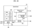
- FIG. 16 is a diagram illustrating a control circuit 170 according to an embodiment of the present disclosure.
- control circuit 170 may include the operation controller 170 A, the address decoder 170 B, the address register 170 C, the page buffer controller 170 D, and the voltage generator controller 170 E.
- the operation controller 170 A may execute an algorithm corresponding to the input command CMD.
- the address decoder 170 B divides the input address ADD into the row address ADDR and the column address ADDC, and output the row address ADDR and the column address ADDC.
- the operation controller 170 A may receive the row address ADDR output from the address decoder 170 B and compare the page address in the received row address ADDR with an index IN of the address register 170 C.
- the address register 170 C may include a table including group(s) GR # and an index IN field in which indices of pages of the groups are identified in association with the corresponding group GR #.
- GR # may identify slow page group(s), and indices of pages in the slow group(s) may be identified in the IN field.
- the index IN may include all page addresses PA 1 to PA 6 in first and second page groups GR 1 and GR 2 . That is, all pages of a slow group including fast pages are identified in the IN field. For example, as shown in FIG.
- the fifth page PG 5 is a fast page, but the second page group GR 2 including the fifth page PG 5 is a slow page group; thus, the fifth page address PA 5 corresponding to the fifth page PG 5 may be included in the index IN of the address register 170 C.
- the operation controller 170 A may compare the page addresses stored in the address register 170 C with the seventh page address PA 7 . When the comparison reveals that PG 7 is not present in the address register 170 C, the operation controller 170 A may generate a page buffer control code PBCD and a voltage generator control code VGCD so that the verify operation in which a first evaluation time is set is performed.
- the page buffer controller 170 D may output the page buffer control signals PBSIG in response to the page buffer control code PBCD, and the voltage generator controller 170 E may output the operation code OPc in response to the voltage generator control code VGCD.
- the operation controller 170 A may compare the page addresses stored in the address register 170 C with the second page address PA 2 . When the comparison reveals that PG 2 is present in the address register 170 C, the operation controller 170 A may generate the page buffer control code PBCD and the voltage generator control code VGCD so that the verify operation in which a second evaluation time shorter than the first evaluation time is set is performed.
- the page buffer controller 170 D may output the page buffer control signals PBSIG in response to the page buffer control code PBCD, and the voltage generator controller 170 E may output the operation code OPc in response to the voltage generator control code VGCD.
- FIG. 17 is a diagram illustrating an embodiment in which the time of an evaluation operation is adjusted according to the number of program pulses.
- the program operation may be performed using an incremental step pulse program (ISPP) method in which the program voltage is gradually increased.
- ISPP incremental step pulse program
- the operation in which the program voltage is applied and the verify operation may form one loop. Therefore, as the number of loops increases, the number of program pulses applied to the selected word line increases.
- the evaluation time may be adjusted according to the number of program pulses PC #.
- the verify operation to which the first evaluation time 1 tEV is applied may be performed at the beginning of programming the memory cells of the erase state ER, and the verify operation to which the second evaluation time 2 tEV shorter than the first evaluation time 1 tEV is applied may be performed in a period in which the threshold voltage is close to the target voltage Vt.
- the verify operation to which the first evaluation time 1 tEV is applied may be performed when the number of program pulses PC # is 1 to 3, and the verify operation to which the second evaluation time 2 tEV is applied may be performed when the number of program pulses PC # is 4 or more.
- FIG. 18 is a diagram illustrating an embodiment of controlling the time of an evaluation operation according to a threshold voltage of memory cells.
- the evaluation time of the verify operation may be adjusted according to the threshold voltage of the slow memory cells. For example, at the beginning of programming the memory cells of the erase state ER, the verify operation to which the first evaluation time 1 tEV is applied may be performed.
- the verify operation to which the first evaluation time 1 tEV is applied may be performed.
- two verify operations may be performed in one loop in the program operation of the cells of which the threshold voltage is not increased to the target voltage Vt. For example, a sub target voltage Vts lower than the target voltage Vt may be set. That is, after the verify operation for the sub target voltage Vts is performed, the verify operation for the target voltage Vt may be successively performed. From a loop in which the sub target voltage Vts is used, the verify operation to which the second evaluation time 2 tEV is applied may be performed.
- FIG. 19 is a diagram illustrating a memory system 70000 according to another embodiment of the present disclosure.
- the memory system 70000 may be implemented as a memory card or a smart card.
- the memory system 70000 may include the semiconductor memory device 1100 , the controller 1200 , and a card interface 7100 .
- the controller 1200 may control data exchange between the memory device 1100 and the card interface 7100 .
- the card interface 7100 may be a secure digital (SD) card interface or a multi-media card (MMC) interface, but the invention is not limited thereto.
- the memory device 1100 may perform a program operation according to the above-described embodiments, and data programmed in the memory device 1100 may be output through the card interface 7100 under control of the controller 1200 .
- the card interface 7100 may interface data exchange between a host 60000 and the controller 1200 according to a protocol of the host 60000 .
- the card interface 7100 may support a universal serial bus (USB) protocol, and an inter chip (IC)-USB protocol.
- USB universal serial bus
- IC inter chip
- the card interface 7100 may refer to hardware capable of supporting a protocol that is used by the host 60000 , software installed in the hardware, or a signal transmission method.
- the host interface 6200 may perform data communication with the memory device 1100 through the card interface 7100 and the controller 1200 under control of a microprocessor ( ⁇ P) 6100 .
- ⁇ P microprocessor
Abstract
Description
Claims (19)
Applications Claiming Priority (2)
| Application Number | Priority Date | Filing Date | Title |
|---|---|---|---|
| KR1020200098765A KR20220018341A (en) | 2020-08-06 | 2020-08-06 | Memory device and operating method of the memory device |
| KR10-2020-0098765 | 2020-08-06 |
Publications (2)
| Publication Number | Publication Date |
|---|---|
| US20220043584A1 US20220043584A1 (en) | 2022-02-10 |
| US11520489B2 true US11520489B2 (en) | 2022-12-06 |
Family
ID=80115036
Family Applications (1)
| Application Number | Title | Priority Date | Filing Date |
|---|---|---|---|
| US17/148,161 Active 2041-01-16 US11520489B2 (en) | 2020-08-06 | 2021-01-13 | Memory device and method of operating the same |
Country Status (3)
| Country | Link |
|---|---|
| US (1) | US11520489B2 (en) |
| KR (1) | KR20220018341A (en) |
| CN (1) | CN114067868A (en) |
Citations (7)
| Publication number | Priority date | Publication date | Assignee | Title |
|---|---|---|---|---|
| US20160019975A1 (en) * | 2014-07-21 | 2016-01-21 | Samsung Electronics Co., Ltd. | Semiconductor memory device and semiconductor memory system including the same |
| US20160172049A1 (en) * | 2014-12-11 | 2016-06-16 | SK Hynix Inc. | Semiconductor device and method of operating the same |
| US20170069384A1 (en) * | 2015-09-03 | 2017-03-09 | SK Hynix Inc. | Memory system and operating method thereof |
| KR101903580B1 (en) | 2014-07-15 | 2018-10-04 | 샌디스크 테크놀로지스 엘엘씨 | Reprogramming memory with single program pulse per data state |
| KR20180125807A (en) | 2017-05-16 | 2018-11-26 | 에스케이하이닉스 주식회사 | Semiconductor memory device and operation method thereof |
| US20190189215A1 (en) * | 2017-12-19 | 2019-06-20 | SK Hynix Inc. | Semiconductor memory device and method of operating the same |
| US20200027519A1 (en) * | 2018-07-23 | 2020-01-23 | SK Hynix Memory Solutions America Inc. | Memory system and method for optimizing read threshold |
-
2020
- 2020-08-06 KR KR1020200098765A patent/KR20220018341A/en unknown
-
2021
- 2021-01-13 US US17/148,161 patent/US11520489B2/en active Active
- 2021-03-01 CN CN202110224116.3A patent/CN114067868A/en active Pending
Patent Citations (7)
| Publication number | Priority date | Publication date | Assignee | Title |
|---|---|---|---|---|
| KR101903580B1 (en) | 2014-07-15 | 2018-10-04 | 샌디스크 테크놀로지스 엘엘씨 | Reprogramming memory with single program pulse per data state |
| US20160019975A1 (en) * | 2014-07-21 | 2016-01-21 | Samsung Electronics Co., Ltd. | Semiconductor memory device and semiconductor memory system including the same |
| US20160172049A1 (en) * | 2014-12-11 | 2016-06-16 | SK Hynix Inc. | Semiconductor device and method of operating the same |
| US20170069384A1 (en) * | 2015-09-03 | 2017-03-09 | SK Hynix Inc. | Memory system and operating method thereof |
| KR20180125807A (en) | 2017-05-16 | 2018-11-26 | 에스케이하이닉스 주식회사 | Semiconductor memory device and operation method thereof |
| US20190189215A1 (en) * | 2017-12-19 | 2019-06-20 | SK Hynix Inc. | Semiconductor memory device and method of operating the same |
| US20200027519A1 (en) * | 2018-07-23 | 2020-01-23 | SK Hynix Memory Solutions America Inc. | Memory system and method for optimizing read threshold |
Also Published As
| Publication number | Publication date |
|---|---|
| US20220043584A1 (en) | 2022-02-10 |
| KR20220018341A (en) | 2022-02-15 |
| CN114067868A (en) | 2022-02-18 |
Similar Documents
| Publication | Publication Date | Title |
|---|---|---|
| CN109935267B (en) | Semiconductor memory device and method of operating the same | |
| CN108281166B (en) | Storage device and operation method thereof | |
| CN112037839B (en) | Semiconductor memory device and method of operating the same | |
| CN111312320B (en) | Semiconductor memory device and method of operating the same | |
| US20220076754A1 (en) | Memory device and method of operating the same | |
| CN110415740B (en) | Controller and operation method thereof | |
| US20210319838A1 (en) | Memory device and method of operating the memory device | |
| US8848450B2 (en) | Method and apparatus for adjusting maximum verify time in nonvolatile memory device | |
| US20220336040A1 (en) | Memory device, memory system including the memory device, and test operation of the memory device | |
| CN112825252B (en) | Memory device and method of operating the same | |
| US11276475B2 (en) | Memory device and method of operating the memory device | |
| US11581028B2 (en) | Memory device for counting fail bits included in sensed data | |
| US11551763B2 (en) | Semiconductor memory device and method of operating the same | |
| US11520489B2 (en) | Memory device and method of operating the same | |
| CN115798552A (en) | Memory device and operation method thereof | |
| US11302408B2 (en) | Memory device | |
| US20240145008A1 (en) | Memory device and operating method of the memory device | |
| US20240127892A1 (en) | Memory device and operating method of the memory device | |
| US20240013837A1 (en) | Memory device and operating method of the memory device | |
| US11646089B2 (en) | Memory device for performing verify operation and operating method thereof | |
| US11205472B2 (en) | Memory device and method of operating the same | |
| US11615847B2 (en) | Memory device and operating method of the memory device | |
| US20230290412A1 (en) | Memory device and program operation method thereof | |
| CN117953926A (en) | Memory device and operation method of memory device | |
| CN115440281A (en) | Memory device related to performing programming operation on memory cell |
Legal Events
| Date | Code | Title | Description |
|---|---|---|---|
| AS | Assignment |
Owner name: SK HYNIX INC., KOREA, REPUBLIC OF Free format text: ASSIGNMENT OF ASSIGNORS INTEREST;ASSIGNOR:YOO, JEONG HO;REEL/FRAME:054909/0205 Effective date: 20201029 |
|
| FEPP | Fee payment procedure |
Free format text: ENTITY STATUS SET TO UNDISCOUNTED (ORIGINAL EVENT CODE: BIG.); ENTITY STATUS OF PATENT OWNER: LARGE ENTITY |
|
| STPP | Information on status: patent application and granting procedure in general |
Free format text: DOCKETED NEW CASE - READY FOR EXAMINATION |
|
| STPP | Information on status: patent application and granting procedure in general |
Free format text: NON FINAL ACTION MAILED |
|
| STPP | Information on status: patent application and granting procedure in general |
Free format text: RESPONSE TO NON-FINAL OFFICE ACTION ENTERED AND FORWARDED TO EXAMINER |
|
| STPP | Information on status: patent application and granting procedure in general |
Free format text: NOTICE OF ALLOWANCE MAILED -- APPLICATION RECEIVED IN OFFICE OF PUBLICATIONS |
|
| STPP | Information on status: patent application and granting procedure in general |
Free format text: PUBLICATIONS -- ISSUE FEE PAYMENT VERIFIED |
|
| STCF | Information on status: patent grant |
Free format text: PATENTED CASE |