US11520437B2 - Touch device having switch circuits controlling between touch electrodes and drive chip, touch system and control method thereof - Google Patents
Touch device having switch circuits controlling between touch electrodes and drive chip, touch system and control method thereof Download PDFInfo
- Publication number
- US11520437B2 US11520437B2 US17/258,153 US202017258153A US11520437B2 US 11520437 B2 US11520437 B2 US 11520437B2 US 202017258153 A US202017258153 A US 202017258153A US 11520437 B2 US11520437 B2 US 11520437B2
- Authority
- US
- United States
- Prior art keywords
- touch
- drive chip
- touch electrodes
- stylus
- switch
- Prior art date
- Legal status (The legal status is an assumption and is not a legal conclusion. Google has not performed a legal analysis and makes no representation as to the accuracy of the status listed.)
- Active
Links
Images


Classifications
-
- G—PHYSICS
- G06—COMPUTING OR CALCULATING; COUNTING
- G06F—ELECTRIC DIGITAL DATA PROCESSING
- G06F3/00—Input arrangements for transferring data to be processed into a form capable of being handled by the computer; Output arrangements for transferring data from processing unit to output unit, e.g. interface arrangements
- G06F3/01—Input arrangements or combined input and output arrangements for interaction between user and computer
- G06F3/03—Arrangements for converting the position or the displacement of a member into a coded form
- G06F3/041—Digitisers, e.g. for touch screens or touch pads, characterised by the transducing means
- G06F3/0416—Control or interface arrangements specially adapted for digitisers
- G06F3/0418—Control or interface arrangements specially adapted for digitisers for error correction or compensation, e.g. based on parallax, calibration or alignment
- G06F3/04186—Touch location disambiguation
-
- G—PHYSICS
- G06—COMPUTING OR CALCULATING; COUNTING
- G06F—ELECTRIC DIGITAL DATA PROCESSING
- G06F3/00—Input arrangements for transferring data to be processed into a form capable of being handled by the computer; Output arrangements for transferring data from processing unit to output unit, e.g. interface arrangements
- G06F3/01—Input arrangements or combined input and output arrangements for interaction between user and computer
- G06F3/03—Arrangements for converting the position or the displacement of a member into a coded form
- G06F3/041—Digitisers, e.g. for touch screens or touch pads, characterised by the transducing means
- G06F3/044—Digitisers, e.g. for touch screens or touch pads, characterised by the transducing means by capacitive means
- G06F3/0446—Digitisers, e.g. for touch screens or touch pads, characterised by the transducing means by capacitive means using a grid-like structure of electrodes in at least two directions, e.g. using row and column electrodes
-
- G—PHYSICS
- G06—COMPUTING OR CALCULATING; COUNTING
- G06F—ELECTRIC DIGITAL DATA PROCESSING
- G06F3/00—Input arrangements for transferring data to be processed into a form capable of being handled by the computer; Output arrangements for transferring data from processing unit to output unit, e.g. interface arrangements
- G06F3/01—Input arrangements or combined input and output arrangements for interaction between user and computer
- G06F3/03—Arrangements for converting the position or the displacement of a member into a coded form
- G06F3/033—Pointing devices displaced or positioned by the user, e.g. mice, trackballs, pens or joysticks; Accessories therefor
- G06F3/0354—Pointing devices displaced or positioned by the user, e.g. mice, trackballs, pens or joysticks; Accessories therefor with detection of two-dimensional [2D] relative movements between the device, or an operating part thereof, and a plane or surface, e.g. 2D mice, trackballs, pens or pucks
- G06F3/03545—Pens or stylus
-
- G—PHYSICS
- G06—COMPUTING OR CALCULATING; COUNTING
- G06F—ELECTRIC DIGITAL DATA PROCESSING
- G06F3/00—Input arrangements for transferring data to be processed into a form capable of being handled by the computer; Output arrangements for transferring data from processing unit to output unit, e.g. interface arrangements
- G06F3/01—Input arrangements or combined input and output arrangements for interaction between user and computer
- G06F3/03—Arrangements for converting the position or the displacement of a member into a coded form
- G06F3/041—Digitisers, e.g. for touch screens or touch pads, characterised by the transducing means
- G06F3/0416—Control or interface arrangements specially adapted for digitisers
- G06F3/04164—Connections between sensors and controllers, e.g. routing lines between electrodes and connection pads
-
- G—PHYSICS
- G06—COMPUTING OR CALCULATING; COUNTING
- G06F—ELECTRIC DIGITAL DATA PROCESSING
- G06F3/00—Input arrangements for transferring data to be processed into a form capable of being handled by the computer; Output arrangements for transferring data from processing unit to output unit, e.g. interface arrangements
- G06F3/01—Input arrangements or combined input and output arrangements for interaction between user and computer
- G06F3/03—Arrangements for converting the position or the displacement of a member into a coded form
- G06F3/041—Digitisers, e.g. for touch screens or touch pads, characterised by the transducing means
- G06F3/0416—Control or interface arrangements specially adapted for digitisers
- G06F3/04166—Details of scanning methods, e.g. sampling time, grouping of sub areas or time sharing with display driving
-
- G—PHYSICS
- G06—COMPUTING OR CALCULATING; COUNTING
- G06F—ELECTRIC DIGITAL DATA PROCESSING
- G06F3/00—Input arrangements for transferring data to be processed into a form capable of being handled by the computer; Output arrangements for transferring data from processing unit to output unit, e.g. interface arrangements
- G06F3/01—Input arrangements or combined input and output arrangements for interaction between user and computer
- G06F3/03—Arrangements for converting the position or the displacement of a member into a coded form
- G06F3/041—Digitisers, e.g. for touch screens or touch pads, characterised by the transducing means
- G06F3/0416—Control or interface arrangements specially adapted for digitisers
- G06F3/0418—Control or interface arrangements specially adapted for digitisers for error correction or compensation, e.g. based on parallax, calibration or alignment
-
- G—PHYSICS
- G06—COMPUTING OR CALCULATING; COUNTING
- G06F—ELECTRIC DIGITAL DATA PROCESSING
- G06F3/00—Input arrangements for transferring data to be processed into a form capable of being handled by the computer; Output arrangements for transferring data from processing unit to output unit, e.g. interface arrangements
- G06F3/01—Input arrangements or combined input and output arrangements for interaction between user and computer
- G06F3/03—Arrangements for converting the position or the displacement of a member into a coded form
- G06F3/041—Digitisers, e.g. for touch screens or touch pads, characterised by the transducing means
- G06F3/044—Digitisers, e.g. for touch screens or touch pads, characterised by the transducing means by capacitive means
- G06F3/0441—Digitisers, e.g. for touch screens or touch pads, characterised by the transducing means by capacitive means using active external devices, e.g. active pens, for receiving changes in electrical potential transmitted by the digitiser, e.g. tablet driving signals
-
- G—PHYSICS
- G06—COMPUTING OR CALCULATING; COUNTING
- G06F—ELECTRIC DIGITAL DATA PROCESSING
- G06F3/00—Input arrangements for transferring data to be processed into a form capable of being handled by the computer; Output arrangements for transferring data from processing unit to output unit, e.g. interface arrangements
- G06F3/01—Input arrangements or combined input and output arrangements for interaction between user and computer
- G06F3/03—Arrangements for converting the position or the displacement of a member into a coded form
- G06F3/041—Digitisers, e.g. for touch screens or touch pads, characterised by the transducing means
- G06F3/044—Digitisers, e.g. for touch screens or touch pads, characterised by the transducing means by capacitive means
- G06F3/0443—Digitisers, e.g. for touch screens or touch pads, characterised by the transducing means by capacitive means using a single layer of sensing electrodes
-
- G—PHYSICS
- G06—COMPUTING OR CALCULATING; COUNTING
- G06F—ELECTRIC DIGITAL DATA PROCESSING
- G06F2203/00—Indexing scheme relating to G06F3/00 - G06F3/048
- G06F2203/041—Indexing scheme relating to G06F3/041 - G06F3/045
- G06F2203/04108—Touchless 2D- digitiser, i.e. digitiser detecting the X/Y position of the input means, finger or stylus, also when it does not touch, but is proximate to the digitiser's interaction surface without distance measurement in the Z direction
-
- G—PHYSICS
- G06—COMPUTING OR CALCULATING; COUNTING
- G06F—ELECTRIC DIGITAL DATA PROCESSING
- G06F3/00—Input arrangements for transferring data to be processed into a form capable of being handled by the computer; Output arrangements for transferring data from processing unit to output unit, e.g. interface arrangements
- G06F3/01—Input arrangements or combined input and output arrangements for interaction between user and computer
- G06F3/03—Arrangements for converting the position or the displacement of a member into a coded form
- G06F3/041—Digitisers, e.g. for touch screens or touch pads, characterised by the transducing means
- G06F3/0416—Control or interface arrangements specially adapted for digitisers
- G06F3/04162—Control or interface arrangements specially adapted for digitisers for exchanging data with external devices, e.g. smart pens, via the digitiser sensing hardware
Definitions
- This disclosure relates to the field of touch display technology, and in particular to a touch device, a touch system and a control method thereof.
- a stylus can be used for the human-computer interaction.
- Embodiments of the disclosure provide a touch device, including:
- a touch screen including: a plurality of touch electrodes, and a plurality of switch circuits corresponding to the plurality of touch electrodes respectively;
- the touch electrodes are coupled to the drive chip through the corresponding switch circuits.
- the drive chip is configured to determine that the touch screen is contacted by an interference object and determine an interference area, according to capacitance values of the touch electrodes during a time period when a stylus is interacting with the touch screen, and disconnect touch electrodes in the interference area from the drive chip through corresponding switch circuits.
- the plurality of switch circuits each includes: at least two first switch transistors.
- An input terminal of each of the at least two first switch transistors is coupled to the drive chip, and an output terminal of each of the at least two first switch transistors is coupled to a respective one of the touch electrodes.
- the plurality of switch circuits each further includes a second switch transistor.
- An input terminal of the second switch transistor is coupled to the drive chip, and an output terminal of the second switch transistor is coupled to input terminals of the at least two first switch transistors in the same switch circuit.
- the drive chip includes a plurality of processors.
- the processors are configured to convert analog signals into digital signals.
- the processors are coupled to the plurality of switch circuits.
- the processors are coupled to the plurality of switch circuits respectively in one-to-one correspondence.
- one of the switch circuits is coupled to at least two of the processors.
- embodiments of the disclosure further provide a touch system, including: the above-mentioned touch device and a stylus matching with the touch device.
- embodiments of the disclosure further provide a control method of the above-mentioned touch system.
- the method includes:
- the plurality of switch circuits each includes at least two first switch transistors.
- the disconnecting, by the drive chip, touch electrodes in the interference area from the drive chip through corresponding switch circuits includes:
- the plurality of switch circuits each includes at least two first switch transistors and a second switch transistor.
- the disconnecting, by the drive chip, touch electrodes in the interference area from the drive chip through corresponding switch circuits includes:
- the method further includes:
- the sending, by the drive chip, the handshake signal to the touch electrodes includes:
- the feeding back, by the stylus, the excitation signal to the touch electrodes after receiving the handshake signal includes:
- the stylus feeding back, by the stylus, the excitation signal to the touch electrodes in at least two consecutive frames after receiving the handshake signal.
- the stylus feeds back the excitation signal once per frame.
- FIG. 1 is a schematic diagram when a user holds a stylus with one hand to write on the touch screen
- FIG. 2 is a schematic diagram in which the stylus writes on the touch screen in the large-area pressing state
- FIG. 3 is a structural schematic diagram of a touch screen in an embodiment of the disclosure.
- FIG. 4 is a timing diagram of the stylus protocol
- FIG. 5 is a schematic diagram of the point reporting process corresponding to the normal writing state shown in FIG. 1 ;
- FIG. 6 is a schematic diagram of the point reporting process corresponding to the large-area pressing state shown in FIG. 2 ;
- FIG. 7 is a principle schematic diagram of failure to report a point in the large-area pressing state
- FIG. 8 is a first structural schematic diagram of a touch device provided by an embodiment of the disclosure.
- FIG. 9 is a second structural schematic diagram of a touch device provided by an embodiment of the disclosure.
- FIG. 10 is a third structural schematic diagram of a touch device provided by an embodiment of the disclosure.
- FIG. 11 is a first flowchart of a control method of the touch device provided by an embodiment of the disclosure.
- FIG. 12 is a second flowchart of a control method of the touch device provided by an embodiment of the disclosure.
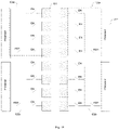
- FIG. 13 is a timing diagram of the stylus in the normal writing state in the case shown in FIG. 1 ;
- FIG. 14 is a timing diagram in the large-area pressing state in the case shown in FIG. 2 ;
- FIG. 15 is a timing diagram corresponding to the control method in an embodiment of the disclosure.
- the touch system realizes the scribing and point reporting functions of the stylus based on the structure of the touch screen shown in FIG. 3 and based on the stylus protocol shown in FIG. 4 .
- a touch screen 10 includes a plurality of touch electrodes 101 and a plurality of touch traveling lines 102 .
- the touch electrodes 101 are coupled to a drive chip through the touch traveling lines 102 , and the drive chip may send a handshake signal to the touch electrodes 101 and also receive the excitation signal collected by the touch electrodes 101 .
- one frame of time period F includes: a handshake signal transmission time period U, a display time period D, and a touch detection time period T.
- the handshake signal transmission time period U is used to transmit the handshake signals W and generally the handshake signal transmission time period U is located at the beginning of one frame of time period F.
- the display time period D is used to transmit the display signals.
- the touch detection time period T is used to transmit the touch detection signals.
- the display time period D is distributed separately from the touch detection time period T, that is, the display signals and the touch detection signals are transmitted at different times.
- the touch detection signals may include a stylus detection signal, a noise detection signal, a finger touch detection signal, and a stylus tilt angle detection signal, etc.
- the number of touch detection time periods T in one frame of time period F can be determined according to the actual needs of the touch screen P. For example, 14 touch detection time periods T may be set in one frame of time period F in FIG. 4 . 8 touch detection time periods T are used to transmit the stylus detection signal, 1 touch detection time period T is used to transmit the noise detection signal, 2 touch detection time periods T are used to transmit the finger touch detection signal, and 2 touch detection time periods T are used to transmit the stylus tilt angle detection signal, which can be configured according to the specifications of the actual product and is not limited here.
- FIG. 5 is a point reporting process corresponding to the normal writing state shown in FIG. 1 .
- the drive chip sends the handshake signal W to the touch electrodes during the handshake signal transmission period U.
- the distance between the stylus and the touch electrode is relatively close and the stylus is in the conductive state, so a coupling capacitance C 1 is formed between the tip of the stylus and the touch electrode, and thus the stylus can receive the handshake signal W through the coupling capacitance C 1 .
- the stylus feeds back an excitation signal G in the touch detection time period T, the touch electrode near the tip of the stylus receives the excitation signal G, and then the drive chip receives the excitation signal G, thereby achieving the point reporting function.
- the drive chip can determine the tip position of the stylus according to the received excitation signal G, and the display data can be formed through subsequent data processing to control the touch screen to display the sliding trajectory of the stylus, achieving the smooth writing function.
- FIG. 6 is a point reporting process corresponding to the large-area pressing state shown in FIG. 2 .
- the user holds the stylus P with one hand to write on the touch screen 10 , and the other hand H presses on the touch screen 10 .
- the user grasps the stylus with the palm of the right hand and presses on the touch screen with the palm of the left hand.
- the palm of the left hand and the touch electrode generate a coupling capacitance C 2
- the palm of the right hand and the stylus form a coupling capacitance C 3 .
- the stylus cannot receive the handshake signal W, or the handshake signal W received by the stylus is relatively weak, so that the requirement of being able to send out the excitation signal G cannot be achieved, the stylus cannot feed back the excitation signal G, the point reporting fails, and thus the broken lines appear.
- the handshake signal W is a square wave signal as an example in FIG. 7 . Since the left hand and the right hand are conductive, the handshake signal W is transmitted from the left hand to the right hand via the touch electrodes when the palm of the left hand presses the touch screen, and the handshake signal W is transmitted to the tip of the stylus when the palm of the right hand grasps the stylus, so that two terminals of the coupling capacitance C 1 formed by the tip of the stylus and the touch electrode are added with the same AC signal and thus the signal cancellation phenomenon occurs, so the transmission of the handshake signal W fails.
- the degree of contact between the palm and the touch screen may be different at different times, so the degree of influence of the coupling capacitances C 2 and C 3 on the transmission of the handshake signal W may change, and thus the on-again-off-again appearance of the lineation of the stylus will occur.
- embodiments of the disclosure provide a touch device, a touch system and a control method thereof.
- Embodiments of the disclosure provide a touch device, as shown in FIG. 8 , which includes:
- a touch screen including: a plurality of touch electrodes 101 , and a plurality of switch circuits 103 corresponding to the touch electrodes 101 respectively;
- the touch electrodes 101 are coupled to the drive chip through the corresponding switch circuits 103 .
- the drive chip is configured to determine that the touch screen is contacted by an interference object and determine the interference area, according to capacitance values of the touch electrodes 101 during a time period when a stylus is interacting with the touch screen, and disconnect touch electrodes 101 in the interference area from the drive chip through corresponding switch circuits 103 .
- a plurality of switch circuits are provided in the touch screen, and the drive chip determines that the touch screen is contacted by an interference object according to the capacitance values of the touch electrodes during a time period when the stylus is interacting with the touch screen and then disconnects touch electrodes in the interference area from the drive chip through the switch circuits corresponding to the touch electrodes in the interference area, so that the signal transmission between the touch electrodes in the interference area and the drive chip can be disconnected, avoiding the effect on the signal transmission between the touch electrodes and the stylus due to the contact of the interference object with the touch screen, and thus avoiding the problem of broken lines.
- the above touch screen in the embodiments of the disclosure may also have the display function, so as to display the sliding trajectory of the stylus.
- the above touch screen may include a display panel and a touch module.
- the touch module may be attached to the light-emitting surface of the display panel, or the touch module may be integrated into the display panel.
- the specific structure of the touch screen is not limited here.
- the above drive chip may be a Touch and Display Driver Integration (TDDI) chip, or the above drive chip may be a non-integrated chip including a touch drive component and a display drive component, which is not limited here.
- TDDI Touch and Display Driver Integration
- the above stylus may match with the above touch device, the above stylus is a conductor, and the stylus has the function of receiving and sending signals, so the stylus can receive the handshake signal of the drive chip and can feed back the excitation signal.
- the drive chip keeps coupling to each touch electrode through a corresponding switch circuit.
- an interference object contacts the touch screen, for example, when a user's palm contacts the touch screen, a coupling capacitance is formed between the palm and the touch electrode, and generally the palm has a greater influence on the capacitance value of the touch electrode, so the interference area of the palm can be determined by detecting the capacitance values of the touch electrodes.
- the interference object may be understood as any object that can affect the interaction between the stylus and the touch screen by contacting the touch screen.
- the principles of other interference objects contacting the touch screen are similar to the principle of the palm contacting the touch screen, and the interference area can also be obtained according to the capacitance value of each touch electrode.
- the drive chip disconnects the touch electrodes in the interference area from the drive chip through corresponding switch circuits, and the touch electrodes in the interference area will not receive the handshake signal, so the contact of the interference object with the touch screen will not affect the signal transmission between the touch electrodes and the stylus, thereby avoiding the phenomenon of broken lines in the sliding trajectory of the stylus.
- the drive chip detects that the contact of the interference object with the touch screen ends, the coupling between the touch electrodes in the interference area and the drive chip can be restored.
- the switch circuit 103 may include: at least two first switch transistors EN.
- the input terminal of the first switch transistor EN is coupled to the drive chip, and the output terminal is coupled to the touch electrode 101 .
- the drive chip is coupled to the touch electrode 101 through the first switch transistor EN, so that the connection state of the touch electrode 101 and the drive chip can be controlled through the corresponding first switch transistor EN.
- the first switch transistor EN can be controlled to be turned on/off by applying a control signal to the gate of the first switch transistor EN.
- the drive chip detects that an interference object contacts the touch screen, so the drive chip controls first switch transistors EN corresponding to touch electrodes 101 in the interference area to be turned off, thereby disconnecting the touch electrodes 101 in the interference area from the drive chip.
- the above switch circuit 103 may further include: a second switch transistor SW.
- the input terminal of the second switch transistor SW is coupled to the drive chip, and the output terminal is coupled to the input terminals of first switch transistors EN in the same switch circuit 103 .
- the wiring between the switching circuit 103 and the drive chip can be reduced, thereby saving the wiring space and wiring cost.
- the second switching transistor SW can be controlled to be turned on/off by applying a control signal to the gate of the second switching transistor SW.
- the connection state of each touch electrode and the drive chip can be controlled. Specifically, if all the touch electrodes 101 corresponding to a switch circuit 103 are in the interference area, then the drive chip controls the second switch transistor SW in the switch circuit 103 to be turned off, that is, controls all the touch electrodes 101 corresponding to the switch circuit 103 to be disconnected from the drive chip.
- the drive chip controls the second switch transistor SW in the switch circuit 103 to be turned on and controls first switch transistors EN corresponding to the part of touch electrodes 101 in the interference area to be turned off, thereby disconnecting the touch electrodes 101 in the interference area from the drive chip, and ensuring that the touch electrodes 101 outside the interference area keep the state of coupling to the drive chip.
- the above drive chip includes: a plurality of processors 201 .
- the processors 201 are configured to convert analog signals into digital signals.
- the processors 201 are coupled to the switch circuits 103 .
- the above processors 201 may convert the received analog signals into digital signals, so that the data processor in the display device can form the corresponding display data according to the digital signals.
- the processors 201 are located in the drive chip, and the drive chip is coupled to the switch circuits 103 through a plurality of processors 201 respectively.
- a plurality of processors 201 are respectively coupled to the switch circuits 103 in one-to-one correspondence, so that the connection state of a processor 201 with the corresponding touch electrodes 101 can be controlled through a corresponding switch circuit 103 .
- one switch circuit 103 is coupled to at least two processors 201 .
- two upper processors 201 are coupled to the corresponding touch electrodes 101 through the same switch circuit 103 a .
- Two lower processors 201 are coupled to the corresponding touch electrodes 101 through the same switch circuit 103 b .
- One second switch transistor SW 1 can be coupled to respective first switch transistors EN in the switch circuit 103 a
- one second switch transistor SW 2 can be coupled to respective first switch transistors EN in the switch circuit 103 b .
- one switch circuit 103 is coupled to two processors 201 as an example for illustration. In a specific implementation, one switch circuit 103 may also be coupled to more processors 201 , which is not limited here.
- embodiments of the disclosure further provide a touch system including: the above touch device, and a stylus matching with the touch device. Since the principle solving the problem of the touch system is similar to that of the above touch device, the implementations of the touch system can refer to the implementations of the above touch device, and the repeated description thereof will be omitted here.
- embodiments of the disclosure further provide a control method of the above touch system. Since the principle solving the problem of the control method is similar to that of the above touch system, the implementations of the control method can refer to the implementations of the above touch system, and the repeated description thereof will be omitted here.
- the control method of the above touch system provided by some embodiments of the disclosure, as shown in FIG. 11 , includes the following steps.
- a drive chip determines that the touch screen is contacted by an interference object and determines the interference area according to capacitance values of the touch electrodes during a time period when the stylus is interacting with the touch screen.
- the drive chip determines that the touch screen is contacted by the interference object according to the capacitance values of the touch electrodes during a time period when the stylus is interacting with the touch screen and then disconnects the touch electrodes in the interference area from the drive chip through the switch circuits, so that the signal transmission between the touch electrodes in the interference area and the drive chip can be disconnected, avoiding the effect on the signal transmission between the touch electrodes and the stylus due to the contact of the interference object with the touch screen, and thus avoiding the problem of broken lines.
- the drive chip keeps coupling to each touch electrode through the switch circuit.
- an interference object contacts the touch screen, for example, when a user's palm contacts the touch screen, a coupling capacitance(s) is/are formed between the palm and the touch electrode(s), and generally the palm has a greater influence on the capacitance value(s) of the touch electrode(s), so the interference area of the palm can be determined by detecting the capacitance values of the touch electrodes.
- the drive chip disconnects the touch electrodes in the interference area from the drive chip through corresponding switch circuits, and the touch electrodes in the interference area will not receive the handshake signal, so the contact of the interference object with the touch screen will not affect the signal transmission between the touch electrodes and the stylus, thereby avoiding the phenomenon of broken lines in the sliding trajectory of the stylus.
- the drive chip detects that the contact of the interference object with the touch screen ends, the coupling between the touch electrodes in the interference area and the drive chip can be restored.
- the switch circuit 103 includes at least two first switch transistors EN.
- the above step S 302 may include:
- the drive chip controls the first switch transistors corresponding to the touch electrodes in the interference area to be turned off, so that the touch electrodes in the interference area can be disconnected from the drive chip.
- the drive chip is coupled to the touch electrode 101 through the first switch transistor EN, so that the connection state of the touch electrode 101 and the drive chip can be controlled through the corresponding first switch transistor EN.
- the first switch transistor EN can be controlled to be turned on/off by applying a control signal to the gate of the first switch transistor EN.
- the switch circuit 103 includes at least two first switch transistors EN and a second switch transistor SW.
- the second switching transistor SW can be controlled to be turned on/off by applying a control signal to the gate of the second switching transistor SW.
- the connection state of each touch electrode and the drive chip can be controlled.
- the above step S 302 may include:
- the drive chip controls the second switch transistor SW in the switch circuit 103 to be turned off, so that all the touch electrodes 101 corresponding to the switch circuit 103 are disconnected from the drive chip;
- the drive chip controls the second switch transistor SW in the switch circuit 103 to be turned on and controls first switch transistors EN corresponding to the part of the touch electrodes 101 in the interference area to be turned off, so that the part of touch electrodes 101 in the interference area can be disconnected from the drive chip while the other part of touch electrodes 101 outside the interference area can still be coupled to the drive chip, ensuring that the stylus can interact with the touch screen smoothly.
- control method provided by the embodiments of the disclosure may further include the following steps.
- the drive chip determines the contact position of the stylus and the touch screen according to the excitation signal received by the touch electrodes, and obtains the sliding trajectory of the stylus.
- the above step S 401 may include:
- the drive chip sends the handshake signal to the touch electrodes frame by frame. Specifically, the drive chip may send the handshake signal W to the touch electrodes during the handshake signal transmission time period U of each frame.
- the drive chip may send the handshake signal to the touch electrodes continuously so as to monitor whether the stylus touches the touch screen at any time.
- the stylus cannot receive the handshake signal, it means that the stylus is far away from the touch screen, and it is possible to make the stylus enter the sleep state to save the power consumption of the stylus.
- step S 402 when the stylus is holden to write on the touch screen, the distance between the stylus and the touch electrode is relatively close and the stylus is in the conductive state, so a coupling capacitance C 1 is formed between the tip of the stylus and the touch electrode, and thus the stylus can receive the handshake signal W through the coupling capacitance C 1 .
- the stylus feeds back an excitation signal G in the touch detection time period T, the touch electrode near the tip of the stylus receives the excitation signal G, and then the drive chip receives the excitation signal G, thereby achieving the point reporting function.
- the touch electrode closer to the tip of the stylus receives the excitation signal with greater intensity, so the drive chip can determine the contact position of the stylus and the touch screen according to the excitation signal received by the touch electrodes, and obtains the sliding trajectory of the stylus through the subsequent data processing.
- the display data can also be formed to control the touch screen to display the sliding trajectory of the stylus, achieving the smooth writing function.
- FIG. 13 is a timing diagram of the stylus in the normal writing state in the case shown in FIG. 1 .
- the drive chip sends the handshake signal W during the handshake signal transmission time period U in each frame of time period F, and the stylus feeds back the excitation signal G after receiving the handshake signal W, thereby completing the smooth writing function.
- FIG. 14 is a timing diagram in the large-area pressing state in the case shown in FIG. 2 .
- the stylus since the stylus receives no handshake signal W, the stylus will not send out the feedback signal G, which causes the phenomenon of broken lines in the two frames of time periods F.
- the above step S 402 may include that:
- the stylus feeds back the excitation signal to the touch electrodes in at least two consecutive frames after receiving the handshake signal, and the stylus feeds back the excitation signal once per frame.
- FIG. 15 is a timing diagram corresponding to the control method in embodiments of the disclosure.
- the stylus receives the handshaking signal W in the first frame of time period F. Even if the stylus fails to receive the handshake signals W in the following three frames of time periods F, the stylus feeds back the excitation signal G in four consecutive frames of time periods F. In FIG. 15 , the stylus feeds back the excitation signal G in at least four consecutive frames as an example. In a specific implementation, the stylus may feed back the excitation signal in at least two consecutive frames after receiving the handshake signal, which is not limited here.
- the stylus After the stylus receives the handshake signal, it indicates that the tip of the stylus is closer to the touch screen. Since one frame of time period has the relatively short time and it is generally impossible for the user to control the stylus to move away from the touch screen immediately after it approaches the touch screen, it can be considered that the distance between the stylus and the touch screen is relatively close in a short period of time when the stylus approaches the touch screen. Therefore, it is considered that the stylus is in the writing state in at least two consecutive frames. Even if no handshake signal is received in a next frame of time period, the stylus still sends out the excitation signal to reduce the probability of broken lines in the lineation.
- a plurality of switch circuits are provided in the touch screen, and the drive chip determines that the touch screen is contacted by an interference object according to the capacitance values of the touch electrodes during a time period when the stylus is interacting with the touch screen and then disconnects the touch electrodes in the interference area from the drive chip through corresponding switch circuits, so that the signal transmission between the touch electrodes in the interference area and the drive chip can be disconnected, avoiding the effect on the signal transmission between the touch electrodes and the stylus due to the contact of the interference object with the touch screen, and thus avoiding the problem of broken lines.
Landscapes
- Engineering & Computer Science (AREA)
- General Engineering & Computer Science (AREA)
- Theoretical Computer Science (AREA)
- Human Computer Interaction (AREA)
- Physics & Mathematics (AREA)
- General Physics & Mathematics (AREA)
- Computer Networks & Wireless Communication (AREA)
- Position Input By Displaying (AREA)
- Control Of Indicators Other Than Cathode Ray Tubes (AREA)
- User Interface Of Digital Computer (AREA)
Abstract
Description
Claims (8)
Applications Claiming Priority (1)
| Application Number | Priority Date | Filing Date | Title |
|---|---|---|---|
| PCT/CN2020/082496 WO2021195984A1 (en) | 2020-03-31 | 2020-03-31 | Touch-control apparatus, touch-control system and control method therefor |
Publications (2)
| Publication Number | Publication Date |
|---|---|
| US20220137784A1 US20220137784A1 (en) | 2022-05-05 |
| US11520437B2 true US11520437B2 (en) | 2022-12-06 |
Family
ID=77926937
Family Applications (1)
| Application Number | Title | Priority Date | Filing Date |
|---|---|---|---|
| US17/258,153 Active US11520437B2 (en) | 2020-03-31 | 2020-03-31 | Touch device having switch circuits controlling between touch electrodes and drive chip, touch system and control method thereof |
Country Status (3)
| Country | Link |
|---|---|
| US (1) | US11520437B2 (en) |
| CN (1) | CN113748404B (en) |
| WO (1) | WO2021195984A1 (en) |
Families Citing this family (1)
| Publication number | Priority date | Publication date | Assignee | Title |
|---|---|---|---|---|
| CN118871880A (en) * | 2023-02-28 | 2024-10-29 | 京东方科技集团股份有限公司 | Touch control driving method, touch control module and display device |
Citations (9)
| Publication number | Priority date | Publication date | Assignee | Title |
|---|---|---|---|---|
| US20100117986A1 (en) * | 2008-11-12 | 2010-05-13 | Tpo Displays Corp. | Capacitive touch panel and capacitance sensing apparatus and method for the same |
| US20120182259A1 (en) * | 2011-01-13 | 2012-07-19 | Samsung Electronics Co., Ltd. | Apparatus and method of identifying touch area |
| CN102722274A (en) | 2012-05-29 | 2012-10-10 | 苏州瀚瑞微电子有限公司 | Touch-control pen system |
| US20130300672A1 (en) | 2012-05-11 | 2013-11-14 | Research In Motion Limited | Touch screen palm input rejection |
| CN103577008A (en) | 2012-08-08 | 2014-02-12 | 乐金显示有限公司 | Display device with touch screen and method of driving the same |
| US20160266673A1 (en) * | 2015-03-09 | 2016-09-15 | Stmicroelectronics Asia Pacific Pte Ltd | Touch rejection for communication between a touch screen device and an active stylus |
| US20170177145A1 (en) | 2015-12-17 | 2017-06-22 | Wacom Co., Ltd. | Touch panel, signal processing device, and coupling method |
| US10739909B1 (en) * | 2019-04-03 | 2020-08-11 | Himax Technologies Limited | Position input system and method |
| US11231815B2 (en) * | 2019-06-28 | 2022-01-25 | Qeexo, Co. | Detecting object proximity using touch sensitive surface sensing and ultrasonic sensing |
Family Cites Families (6)
| Publication number | Priority date | Publication date | Assignee | Title |
|---|---|---|---|---|
| CN101017419B (en) * | 2005-06-30 | 2010-05-12 | 智点科技(深圳)有限公司 | Touch control panel display |
| JP2007035971A (en) * | 2005-07-27 | 2007-02-08 | Pentel Corp | Capacitance switch control device |
| JP5034365B2 (en) * | 2006-08-09 | 2012-09-26 | パナソニック株式会社 | Input device |
| CN102033668A (en) * | 2009-09-30 | 2011-04-27 | 智点科技(深圳)有限公司 | Capacitive touch screen |
| US8508493B2 (en) * | 2010-06-21 | 2013-08-13 | Pixart Imaging Inc. | Reduction of electromagnetic interference in a capacitive touchscreen system |
| CN103413538B (en) * | 2013-08-27 | 2016-01-06 | 信利半导体有限公司 | Section type liquid crystal display driving circuit and driving method |
-
2020
- 2020-03-31 US US17/258,153 patent/US11520437B2/en active Active
- 2020-03-31 WO PCT/CN2020/082496 patent/WO2021195984A1/en not_active Ceased
- 2020-03-31 CN CN202080000452.3A patent/CN113748404B/en active Active
Patent Citations (11)
| Publication number | Priority date | Publication date | Assignee | Title |
|---|---|---|---|---|
| US20100117986A1 (en) * | 2008-11-12 | 2010-05-13 | Tpo Displays Corp. | Capacitive touch panel and capacitance sensing apparatus and method for the same |
| US20120182259A1 (en) * | 2011-01-13 | 2012-07-19 | Samsung Electronics Co., Ltd. | Apparatus and method of identifying touch area |
| US20130300672A1 (en) | 2012-05-11 | 2013-11-14 | Research In Motion Limited | Touch screen palm input rejection |
| CN102722274A (en) | 2012-05-29 | 2012-10-10 | 苏州瀚瑞微电子有限公司 | Touch-control pen system |
| CN103577008A (en) | 2012-08-08 | 2014-02-12 | 乐金显示有限公司 | Display device with touch screen and method of driving the same |
| US20140043284A1 (en) | 2012-08-08 | 2014-02-13 | Lg Display Co., Ltd. | Display device with touch screen and method of driving the same |
| US20160266673A1 (en) * | 2015-03-09 | 2016-09-15 | Stmicroelectronics Asia Pacific Pte Ltd | Touch rejection for communication between a touch screen device and an active stylus |
| US20170177145A1 (en) | 2015-12-17 | 2017-06-22 | Wacom Co., Ltd. | Touch panel, signal processing device, and coupling method |
| CN107066136A (en) | 2015-12-17 | 2017-08-18 | 株式会社和冠 | Touch panel, signal processing apparatus and coupling method |
| US10739909B1 (en) * | 2019-04-03 | 2020-08-11 | Himax Technologies Limited | Position input system and method |
| US11231815B2 (en) * | 2019-06-28 | 2022-01-25 | Qeexo, Co. | Detecting object proximity using touch sensitive surface sensing and ultrasonic sensing |
Also Published As
| Publication number | Publication date |
|---|---|
| CN113748404B (en) | 2023-01-10 |
| CN113748404A (en) | 2021-12-03 |
| US20220137784A1 (en) | 2022-05-05 |
| WO2021195984A1 (en) | 2021-10-07 |
Similar Documents
| Publication | Publication Date | Title |
|---|---|---|
| US9086749B2 (en) | System and method for improved processing of touch sensor data | |
| US9041687B2 (en) | Communication method for capacitive touch panel | |
| CN107390934B (en) | Display panel and display device | |
| US11354931B2 (en) | Fingerprint sensing device and operation method thereof | |
| CN107463295A (en) | Display panel, driving method thereof, and display device | |
| US20110043466A1 (en) | Touch screen liquid crystal display device | |
| US11520437B2 (en) | Touch device having switch circuits controlling between touch electrodes and drive chip, touch system and control method thereof | |
| US11842004B2 (en) | Method of signal transmission, touch control chip and electronic device | |
| US11847277B2 (en) | Touch circuit and method for controlling touch circuit | |
| CN203299789U (en) | Intelligent touch control device | |
| US20160349898A1 (en) | Touch Control Module for Touch Device and Related Touch Control Method | |
| US8289069B2 (en) | Touch apparatus | |
| CN212460555U (en) | Touch signal processing system | |
| CN210155656U (en) | Interactive flat plate with Type-C interface and interactive flat plate system | |
| CN111599303A (en) | LED display touch module and equipment | |
| US10996790B2 (en) | Touch system | |
| CN202257560U (en) | Novel USB (universal serial bus) switcher equipment | |
| CN209496344U (en) | Touch display unit and electronic equipment | |
| CN110334043A (en) | An interactive flat panel with a Type-C interface and an interactive flat panel system | |
| US11556212B2 (en) | Device and method for capacitive sensing | |
| CN116301434A (en) | Touch display panel, touch driving method thereof and touch display device | |
| CN203276219U (en) | Touch screen testing system | |
| CN210270850U (en) | Hand-writing and reading equipment | |
| CN208110561U (en) | Intelligent touch induction system | |
| CN112347016A (en) | Dual-video input switching device and control method of tablet computer |
Legal Events
| Date | Code | Title | Description |
|---|---|---|---|
| AS | Assignment |
Owner name: BOE TECHNOLOGY GROUP CO., LTD., CHINA Free format text: ASSIGNMENT OF ASSIGNORS INTEREST;ASSIGNORS:FANG, ZHIXIANG;YANG, GUANGLEI;REEL/FRAME:054904/0532 Effective date: 20200902 Owner name: HEFEI BOE OPTOELECTRONICS TECHNOLOGY CO., LTD., CHINA Free format text: ASSIGNMENT OF ASSIGNORS INTEREST;ASSIGNORS:FANG, ZHIXIANG;YANG, GUANGLEI;REEL/FRAME:054904/0532 Effective date: 20200902 |
|
| FEPP | Fee payment procedure |
Free format text: ENTITY STATUS SET TO UNDISCOUNTED (ORIGINAL EVENT CODE: BIG.); ENTITY STATUS OF PATENT OWNER: LARGE ENTITY |
|
| STPP | Information on status: patent application and granting procedure in general |
Free format text: NON FINAL ACTION MAILED |
|
| STPP | Information on status: patent application and granting procedure in general |
Free format text: RESPONSE TO NON-FINAL OFFICE ACTION ENTERED AND FORWARDED TO EXAMINER |
|
| STPP | Information on status: patent application and granting procedure in general |
Free format text: NOTICE OF ALLOWANCE MAILED -- APPLICATION RECEIVED IN OFFICE OF PUBLICATIONS |
|
| AS | Assignment |
Owner name: BEIJING BOE TECHNOLOGY DEVELOPMENT CO., LTD., CHINA Free format text: ASSIGNMENT OF ASSIGNORS INTEREST;ASSIGNOR:BOE TECHNOLOGY GROUP CO., LTD.;REEL/FRAME:061626/0318 Effective date: 20221101 |
|
| STPP | Information on status: patent application and granting procedure in general |
Free format text: PUBLICATIONS -- ISSUE FEE PAYMENT VERIFIED |
|
| STCF | Information on status: patent grant |
Free format text: PATENTED CASE |