US11513650B2 - Transparent touch display device - Google Patents
Transparent touch display device Download PDFInfo
- Publication number
- US11513650B2 US11513650B2 US17/319,976 US202117319976A US11513650B2 US 11513650 B2 US11513650 B2 US 11513650B2 US 202117319976 A US202117319976 A US 202117319976A US 11513650 B2 US11513650 B2 US 11513650B2
- Authority
- US
- United States
- Prior art keywords
- touch
- sensor
- light emitting
- metal
- bridge
- Prior art date
- Legal status (The legal status is an assumption and is not a legal conclusion. Google has not performed a legal analysis and makes no representation as to the accuracy of the status listed.)
- Active
Links
Images


Classifications
-
- G—PHYSICS
- G06—COMPUTING OR CALCULATING; COUNTING
- G06F—ELECTRIC DIGITAL DATA PROCESSING
- G06F3/00—Input arrangements for transferring data to be processed into a form capable of being handled by the computer; Output arrangements for transferring data from processing unit to output unit, e.g. interface arrangements
- G06F3/01—Input arrangements or combined input and output arrangements for interaction between user and computer
- G06F3/03—Arrangements for converting the position or the displacement of a member into a coded form
- G06F3/041—Digitisers, e.g. for touch screens or touch pads, characterised by the transducing means
- G06F3/0412—Digitisers structurally integrated in a display
-
- G—PHYSICS
- G06—COMPUTING OR CALCULATING; COUNTING
- G06F—ELECTRIC DIGITAL DATA PROCESSING
- G06F3/00—Input arrangements for transferring data to be processed into a form capable of being handled by the computer; Output arrangements for transferring data from processing unit to output unit, e.g. interface arrangements
- G06F3/01—Input arrangements or combined input and output arrangements for interaction between user and computer
- G06F3/03—Arrangements for converting the position or the displacement of a member into a coded form
- G06F3/041—Digitisers, e.g. for touch screens or touch pads, characterised by the transducing means
- G06F3/044—Digitisers, e.g. for touch screens or touch pads, characterised by the transducing means by capacitive means
- G06F3/0446—Digitisers, e.g. for touch screens or touch pads, characterised by the transducing means by capacitive means using a grid-like structure of electrodes in at least two directions, e.g. using row and column electrodes
-
- G—PHYSICS
- G06—COMPUTING OR CALCULATING; COUNTING
- G06F—ELECTRIC DIGITAL DATA PROCESSING
- G06F3/00—Input arrangements for transferring data to be processed into a form capable of being handled by the computer; Output arrangements for transferring data from processing unit to output unit, e.g. interface arrangements
- G06F3/01—Input arrangements or combined input and output arrangements for interaction between user and computer
- G06F3/03—Arrangements for converting the position or the displacement of a member into a coded form
- G06F3/041—Digitisers, e.g. for touch screens or touch pads, characterised by the transducing means
- G06F3/0416—Control or interface arrangements specially adapted for digitisers
- G06F3/04166—Details of scanning methods, e.g. sampling time, grouping of sub areas or time sharing with display driving
-
- G—PHYSICS
- G06—COMPUTING OR CALCULATING; COUNTING
- G06F—ELECTRIC DIGITAL DATA PROCESSING
- G06F3/00—Input arrangements for transferring data to be processed into a form capable of being handled by the computer; Output arrangements for transferring data from processing unit to output unit, e.g. interface arrangements
- G06F3/01—Input arrangements or combined input and output arrangements for interaction between user and computer
- G06F3/03—Arrangements for converting the position or the displacement of a member into a coded form
- G06F3/041—Digitisers, e.g. for touch screens or touch pads, characterised by the transducing means
- G06F3/047—Digitisers, e.g. for touch screens or touch pads, characterised by the transducing means using sets of wires, e.g. crossed wires
-
- H—ELECTRICITY
- H10—SEMICONDUCTOR DEVICES; ELECTRIC SOLID-STATE DEVICES NOT OTHERWISE PROVIDED FOR
- H10K—ORGANIC ELECTRIC SOLID-STATE DEVICES
- H10K50/00—Organic light-emitting devices
- H10K50/80—Constructional details
- H10K50/84—Passivation; Containers; Encapsulations
- H10K50/842—Containers
- H10K50/8426—Peripheral sealing arrangements, e.g. adhesives, sealants
-
- H—ELECTRICITY
- H10—SEMICONDUCTOR DEVICES; ELECTRIC SOLID-STATE DEVICES NOT OTHERWISE PROVIDED FOR
- H10K—ORGANIC ELECTRIC SOLID-STATE DEVICES
- H10K59/00—Integrated devices, or assemblies of multiple devices, comprising at least one organic light-emitting element covered by group H10K50/00
- H10K59/10—OLED displays
- H10K59/12—Active-matrix OLED [AMOLED] displays
- H10K59/131—Interconnections, e.g. wiring lines or terminals
-
- H—ELECTRICITY
- H10—SEMICONDUCTOR DEVICES; ELECTRIC SOLID-STATE DEVICES NOT OTHERWISE PROVIDED FOR
- H10K—ORGANIC ELECTRIC SOLID-STATE DEVICES
- H10K59/00—Integrated devices, or assemblies of multiple devices, comprising at least one organic light-emitting element covered by group H10K50/00
- H10K59/40—OLEDs integrated with touch screens
-
- G—PHYSICS
- G06—COMPUTING OR CALCULATING; COUNTING
- G06F—ELECTRIC DIGITAL DATA PROCESSING
- G06F2203/00—Indexing scheme relating to G06F3/00 - G06F3/048
- G06F2203/041—Indexing scheme relating to G06F3/041 - G06F3/045
- G06F2203/04111—Cross over in capacitive digitiser, i.e. details of structures for connecting electrodes of the sensing pattern where the connections cross each other, e.g. bridge structures comprising an insulating layer, or vias through substrate
-
- G—PHYSICS
- G06—COMPUTING OR CALCULATING; COUNTING
- G06F—ELECTRIC DIGITAL DATA PROCESSING
- G06F2203/00—Indexing scheme relating to G06F3/00 - G06F3/048
- G06F2203/041—Indexing scheme relating to G06F3/041 - G06F3/045
- G06F2203/04112—Electrode mesh in capacitive digitiser: electrode for touch sensing is formed of a mesh of very fine, normally metallic, interconnected lines that are almost invisible to see. This provides a quite large but transparent electrode surface, without need for ITO or similar transparent conductive material
Definitions
- the present disclosure relates to a transparent touch display device.
- display devices are being developed in various types, such as a liquid crystal display device and an organic light emitting display device.
- various display technologies and convergence technologies are being developed to meet various user needs.
- a touch sensor configuration including touch electrodes and touch routing wirings must be formed on the panel.
- the inventors of the present disclosure have recognized that the touch sensor configurations utilized in the related art may be a factor that lowers the transmittance of the transparent touch display device. The inventors have further appreciated that for this reason, the development of a transparent display device capable of providing high touch sensitivity while providing high transmittance has not been successful in the related art. The inventors have also recognized the technical problem of unwanted image anomalies occurring based on the touch sensor configurations designed to provide high transmittance in the related art. The inventors have provided one or more embodiments that address one or more technical problems in the related art including the above-mentioned problems.
- One or more embodiments of the present disclosure provide a transparent touch display device including touch sensor configurations having a low reflection structure.
- embodiments of the present disclosure provide a transparent touch display device that enables high transparency, high image quality, and high touch sensitivity.
- embodiments of the present disclosure provide a transparent touch display device that enables high transparency, high image quality, and high touch sensitivity without increasing process complexity.
- embodiments of the present disclosure can provide a transparent touch display device that includes a touch sensor structure and enables high transparency, prevention of image abnormalities and reduction of process complexity under a structure without a polarizing plate.
- a transparent touch display device comprising: a display panel including a display area in which an image is displayed and a non-display area positioned outside the display area, wherein the display area includes a plurality of light emitting areas and a plurality of transmissive areas, and the display panel includes a plurality of subpixels corresponding to the plurality of light emitting areas, a plurality of data lines, a plurality of gate lines, and a plurality of touch electrodes; a data driving circuit configured to drive the plurality of data lines; a gate driving circuit configured to drive the plurality of gate lines; and a touch driving circuit configured to drive the plurality of touch electrodes.
- Each of the plurality of touch electrodes includes a mesh-type sensor metal having a plurality of openings, a sensor transmission layer on the sensor metal, and a sensor auxiliary metal on the sensor transmission layer.
- Part of an incident light incident on the upper surface of the sensor auxiliary metal is reflected from the upper surface of the sensor auxiliary metal, and another part of the incident light incident on the upper surface of the sensor auxiliary metal is reflected from the upper surface of the sensor metal after passing through the sensor auxiliary metal and the sensor transmission layer.
- a phase difference between a first reflected light reflected from the upper surface of the sensor auxiliary metal and a second reflected light reflected from the upper surface of the sensor metal may be an odd multiple of a half wavelength.
- a transparent touch display device comprising: a substrate including a display area in which an image is displayed and a non-display area positioned outside the display area, the display area including a plurality of light emitting areas and a plurality of transmissive areas; a plurality of light emitting devices disposed over the substrate; an encapsulation layer disposed on the plurality of light emitting devices; and a plurality of touch electrodes disposed on or over the encapsulation layer.
- Each of the plurality of touch electrodes includes a mesh-type sensor metal having a plurality of openings, a sensor transmission layer on the sensor metal, and a sensor auxiliary metal on the sensor transmission layer.
- Part of an incident light incident on the upper surface of the sensor auxiliary metal is reflected from the upper surface of the sensor auxiliary metal, and another part of the incident light incident on the upper surface of the sensor auxiliary metal is reflected from the upper surface of the sensor metal after passing through the sensor auxiliary metal and the sensor transmission layer.
- a phase difference between a first reflected light reflected from the upper surface of the sensor auxiliary metal and a second reflected light reflected from the upper surface of the sensor metal may be an odd multiple of a half wavelength.
- a transparent touch display device including touch sensor configurations having a low reflection structure.
- a transparent touch display device that enables high transparency, high image quality and high touch sensitivity.
- a transparent touch display device that includes a touch sensor structure and enables high transparency, prevention of image abnormalities and reduction of process complexity under a structure without a polarizing plate.
- FIG. 1 is a system configuration diagram of a transparent touch display device according to embodiments of the present disclosure.
- FIGS. 2 to 4 are diagrams illustrating arrangements of light emitting areas and transmissive areas in the transparent touch display device according to embodiments of the present disclosure.
- FIG. 5 is a diagram illustrating a schematic structure of a display panel of the transparent touch display device according to embodiments of the present disclosure.
- FIGS. 6 and 7 are a top plan view and a sectional view of the display panel of the transparent touch display device according to embodiments of the present disclosure.
- FIG. 8 is a plan view of an area in which first to fourth touch electrodes are formed in the display panel of the transparent touch display device according to embodiments of the present disclosure.
- FIG. 9 is a diagram schematically illustrating a sectional structure of each of a light emitting area and a transmissive area in the display panel of the transparent touch display device according to embodiments of the present disclosure.
- FIG. 10 is a sectional view of a touch electrode having a low reflection structure in the display panel of the transparent touch display device according to embodiments of the present disclosure.
- FIGS. 11 and 12 are sectional views of an area where a first bridge electrode and a second bridge electrode intersect in the display panel of the transparent touch display device according to embodiments of the present disclosure.
- FIG. 13 is a sectional view of the display panel of the transparent touch display device according to embodiments of the present disclosure, and is a sectional view of the display panel to which the touch electrode having the low reflection structure is applied.
- FIGS. 14 and 15 are a plan view showing mesh pattern structure of first to fourth touch electrodes having the low reflection structure and an enlarged plan view of a partial area of the plan view, when the arrangement structure of FIG. 2 is applied in the display panel of the transparent touch display device according to embodiments of the present disclosure.
- FIGS. 16 and 17 are plan views showing mesh pattern structure of the touch electrode having the low reflection structure, when the arrangement structure of FIGS. 3 and 4 are applied in the display panel of the transparent touch display device according to embodiments of the present disclosure.
- first element is connected or coupled to”, “contacts or overlaps”, etc., a second element
- first element is connected or coupled to”, “contacts or overlaps”, etc.
- second element it should be interpreted that, not only can the first element “be directly connected or coupled to” or “directly contact or overlap” the second element, but a third element can also be “interposed” between the first and second elements, or the first and second elements can “be connected or coupled to”, “contact or overlap”, etc., each other via a fourth element.
- the second element may be included in at least one of two or more elements that “are connected or coupled to”, “contact or overlap”, etc., each other.
- time relative terms such as “after,” “subsequent to,” “next,” “before,” and the like, are used to describe processes or operations of elements or configurations, or flows or steps in operating, processing, manufacturing methods, these terms may be used to describe non-consecutive or non-sequential processes or operations unless the term “directly” or “immediately” is used together.
- FIG. 1 is a system configuration diagram of a transparent touch display device 100 according to embodiments of the present disclosure.
- the transparent touch display device 100 may include a display panel 110 , a data driving circuit 120 , a gate driving circuit 130 , and a display controller 140 as components for displaying an image.
- the display panel 110 may include a display area DA in which an image is displayed and a non-display area NDA in which an image is not displayed.
- the non-display area NDA may be an outer area of the display area DA, and may also be referred to as a bezel area.
- the non-display area NDA may be an area visible from the front surface of the transparent touch display device 100 or may be an area that is bent and not visible from the front surface of the transparent touch display device 100 .
- the display panel 110 may include a plurality of subpixels SP. Also, the display panel 110 may further include various types of signal wires to drive the plurality of subpixels SP.
- the transparent touch display device 100 may be various types of display devices including a LCD (Liquid Crystal Display) device, an OLED (Organic Light emitting Diode) display device, a micro LED (Light Emitting Diode) display device, a quantum dot display device, and the like.
- LCD Liquid Crystal Display
- OLED Organic Light emitting Diode
- micro LED Light Emitting Diode
- quantum dot display device and the like.
- each of the plurality of subpixels SP may vary according to the type of the transparent touch display device 100 .
- each subpixel SP may include a light emitting device (e.g., OLED, etc.) that emits light by itself, one or more transistors, and one or more capacitors.
- various types of signal lines may include a plurality of data lines transferring data signals and a plurality of gate lines transferring gate signals.
- the data signals are also referred to as data voltages or image signals
- the gate signals are also referred to as scan signals.
- the plurality of data lines and the plurality of gate lines may cross each other.
- Each of the plurality of data lines may be disposed while extending in a first direction.
- Each of the plurality of gate lines may be disposed while extending in the second direction.
- the first direction may be a column direction and the second direction may be a row direction.
- the first direction is transverse to the second direction and the first and second directions are not necessarily perpendicular to each other.
- a column direction and a row direction are relative to each other.
- a column direction may be a vertical direction and a row direction may be a horizontal direction.
- a column direction may be a horizontal direction and a row direction may be a vertical direction.
- the data driving circuit 120 is a circuit for driving the plurality of data lines, and may output data signals through the plurality of data lines.
- the gate driving circuit 130 is a circuit for driving the plurality of gate lines, and may output gate signals through the plurality of gate lines.
- the display controller 140 is a device for controlling the data driving circuit 120 and the gate driving circuit 130 , and may control driving timings for the plurality of data lines and driving timings for the plurality of gate lines.
- the display controller 140 supplies a data driving control signal to the data driving circuit 120 to control the data driving circuit 120 , and supplies the gate driving control signal to the gate driving circuit 130 to control the gate driving circuit 130 .
- the data driving circuit 120 may supply data signals to the plurality of data lines according to the driving timing control of the display controller 140 .
- the data driving circuit 120 may receive digital image data from the display controller 140 , convert the received image data into analog data signals, and output them to the plurality of data lines.
- the gate driving circuit 130 may supply gate signals to the plurality of gate lines according to timing control of the display controller 140 .
- the gate driving circuit 130 may receive a first gate voltage corresponding to a turn-on level voltage and a second gate voltage corresponding to a turn-off level voltage together with various gate driving control signals (e.g., a start signal, a reset signal, etc.).
- the gate driving circuit 130 may generate gate signals having the first gate voltage or the second gate voltage, and supply the generated gate signals to the plurality of gate lines.
- the transparent touch display device 100 may include a touch panel and a touch sensing circuit 150 to further provide a touch sensing function as well as an image display function.
- the touch sensing circuit 150 may sense the touch panel to detect whether a touch is generated by a touch object such as a finger or a pen, or detect a touch position.
- the touch sensing circuit 150 may include a touch driving circuit 160 and a touch controller 170 .
- the touch driving circuit 160 may drive and sense the touch panel to generate and output touch sensing data.
- the touch controller 170 may detect the occurrence of a touch or detect a touch position using touch sensing data output from the touch driving circuit 160 .
- the touch panel may include a plurality of touch electrodes as sensors.
- the touch panel may further include a plurality of touch routing wirings for electrically connecting the plurality of touch electrodes and the touch driving circuit 160 .
- the touch panel or touch electrode may be also referred to as a touch sensor.
- the touch panel may exist outside the display panel 110 or may exist inside the display panel 110 .
- the touch panel is referred to as an external type.
- the touch panel is the external type, the touch panel and the display panel 110 may be separately manufactured and combined.
- the external touch panel may include a substrate and a plurality of touch electrodes on the substrate.
- the touch panel is referred to as a built-in type (internal type, embedded type).
- the touch panel is the built-in type, the touch panel may be formed in the display panel 110 during the manufacturing process of the display panel 110 .
- the touch driving circuit 160 may generate touch sensing data by supplying a touch driving signal to all or part of the plurality of touch electrodes and sensing at least one of the plurality of touch electrodes.
- the touch sensing circuit 150 may perform touch sensing using a self-capacitance sensing method or a mutual-capacitance sensing method.
- the touch sensing circuit 150 may perform touch sensing based on the capacitance between each touch electrode and a touch object (e.g., finger, pen, etc.).
- a touch object e.g., finger, pen, etc.
- the touch sensing circuit 150 may perform touch sensing based on capacitance between the touch electrodes.
- the plurality of touch electrodes are divided into driving touch electrodes and sensing touch electrodes.
- the touch driving circuit 160 may drive driving touch electrodes and sense sensing touch electrodes.
- each of the plurality of touch electrodes may serve as a driving touch electrode and a sensing touch electrode.
- the touch driving circuit 160 may drive all or part of the plurality of touch electrodes and sense all or part of the plurality of touch electrodes.
- the touch driving circuit 160 and the touch controller 170 may be implemented as separate devices, or may be implemented by being integrated into a single device.
- the touch driving circuit 160 and the data driving circuit 120 may be implemented by being integrated into a single device.
- FIGS. 2 to 4 are diagrams illustrating arrangements of light emitting areas EA and transmissive areas TA in the transparent touch display device 100 according to embodiments of the present disclosure.
- the subpixels SP of the transparent touch display device 100 may include a first color subpixel emitting a first color light, a second color subpixel emitting a second color light, and a third color subpixel emitting a third color light.
- each of the first color, the second color, and the third color may be one of red, green, and blue.
- the subpixels SP of the transparent touch display device 100 may include a first color subpixel emitting a first color light, a second color subpixel emitting a second color light, a third color subpixel emitting a third color light, and a fourth color subpixel emitting a fourth color light.
- each of the first color, the second color, the third color, and the fourth color may be one of red, green, blue, and white.
- the display panel 110 of the transparent touch display device 100 may include light emitting areas EA of subpixels SP and transmissive areas TA adjacent to the light emitting areas EA.
- the light emitting area EA of the subpixel SP may correspond to an area in which the pixel electrode of the subpixel SP is disposed.
- the light emitting area EA of the subpixel SP may correspond to an area where the pixel electrode, the light emitting layer, and the common electrode constituting the light emitting device (e.g., OLED) of the subpixel SP overlap.
- the area of the light emitting area EA for each color may be variously designed.
- the area of the light emitting area EA of the first color subpixel e.g., Red SP
- the area of the light emitting area EA of the second color subpixel e.g., Green SP
- the area of the light emitting area EA of the third color subpixel e.g., Blue SP
- the area of the light emitting area EA of the second color subpixel (e.g., Green SP) and the area of the light emitting area EA of the third color subpixel (e.g., Blue SP) may be the same or similar within a predetermined range.
- the area of each of the light emitting area EA of the second color subpixel (e.g., Green SP) and the light emitting area EA of the third color subpixel (e.g., Blue SP) may be larger than the area of the light emitting area EA of the first color subpixel (e.g., Red SP) by a predetermined value.
- the area of the light emitting area EA of the first color subpixel e.g., Red SP
- the area of the light emitting area EA of the second color subpixel e.g., Green SP
- the area of the light emitting area EA of the third color subpixel e.g., Blue SP
- the area of the light emitting area EA of the fourth color subpixel e.g., White SP
- the area of each transmissive area TA may be determined.
- the transmittance of the display panel 110 may increase. As the ratio of the areas of the transmissive areas TA to the areas of the light emitting areas EA decreases, the transmittance of the display panel 110 may decrease.
- the transmittance and the transmissive area TA described in the present specification may be referred to as transparency and the transparent area.
- Each of the transmissive areas TA included in the display panel 110 may have the same area. Alternatively, an area of one of the transmissive areas TA included in the display panel 110 may be different from an area of the other transmissive area TA.
- the light emitting areas EA and the transmissive areas TA may be arranged in various forms.
- the light emitting areas EA of the first color subpixels are arranged apart from each other in the first direction (e.g., row direction), and the light emitting areas EA of the second color subpixels (e.g., Green SP) and the light emitting areas EA of the third color subpixels (e.g., Blue SP) may be alternately disposed between the light emitting areas EA of the first color subpixels (e.g., Red SP).
- the light emitting areas EA of the first color subpixels are arranged apart from each other in the first direction
- the light emitting areas EA of the third color subpixel e.g., Blue SP
- the light emitting areas EA of the second color subpixel e.g., Green SP
- the light emitting areas EA of the first color subpixels e.g., Red SP
- the light emitting areas EA of the first color subpixels e.g., Red SP
- the light emitting areas EA of the second color subpixels e.g., Green SP
- the light emitting areas EA of the third color subpixels e.g., Blue SP
- transmissive areas TA may be disposed between light emitting area rows (i-th EA Row, (i+1)-th EA Row, (i+2)-th EA Row) disposed adjacent to each other in the second direction.
- the transmissive areas TA may be disposed between the i-th light emitting area row (i-th EA Row) and the (i+1)-th light emitting area row ((i+1)-th EA Row).
- the transmissive areas TA may be disposed between the (i+1)-th light emitting area row ((i+1)-th EA Row) and the (i+2)-th light emitting area row ((i+2)-th EA Row).
- the transmissive area TA between the light emitting areas EA of the first color subpixels (e.g., Red SP) disposed adjacent in the second direction (e.g., column direction) may be extended to the area between the light emitting area EA of the second color pixel (e.g., Green SP) and the light emitting area EA of the third color pixel (e.g., Blue SP) disposed adjacent in the second direction (e.g., column direction).
- each of the data lines DL may be disposed while extending in a second direction (e.g., column direction).
- Each of the data lines DL may be disposed while avoiding the transmissive areas TA.
- Each of the gate lines GL may be disposed to extend in a first direction (e.g., row direction).
- the gate lines GL may be disposed to overlap the i-th light emitting area row (i-th EA Row), the (i+1)-th light emitting area row ((i+1)-th EA Row), and the (i+2)-th light emitting area row ((i+2)-th EA Row).
- the gate lines GL may be disposed while avoiding the transmissive areas TA.
- the light emitting area EA of the first color subpixel e.g., Red SP
- the light emitting area EA of the second color subpixel e.g., Green SP
- the light emitting areas EA of the three-color subpixel e.g., Blue SP
- a first direction e.g., row direction
- the transmissive areas TA are disposed between adjacent light emitting area rows (i-th EA Row, (i+1)-th EA Row) in the second direction (e.g., column direction).
- each of the data lines DL may be disposed while extending in the second direction.
- Each of the data lines DL may be disposed while avoiding the transmissive areas TA.
- Each of the gate lines GL may be disposed while extending in the first direction.
- the gate lines GL may be disposed to overlap each light emitting area row (i-th EA Row, (i+1)-th EA Row).
- the gate lines GL may be disposed while avoiding the transmissive areas TA.
- the light emitting area EA of the first color subpixel e.g., Red SP
- the light emitting area EA of the second color subpixel e.g., Green SP
- the light emitting area EA of the third color subpixel e.g., Blue SP
- the light emitting area EA of the fourth color subpixel e.g., White SP
- the second direction e.g., column direction
- the transmissive areas TA may be disposed between adjacent light emitting area columns (j-th EA Column, (j+1)-th EA Column) in the first direction.
- each of the data lines DL may be disposed while extending in the second direction.
- Each of the data lines DL may be disposed while avoiding the transmissive areas TA.
- Each of the gate lines GL may be disposed while extending in the first direction.
- the gate lines GL may be disposed between the light emitting area rows.
- the gate lines GL may be disposed between the transmissive areas TA while avoiding the transmissive areas TA.
- FIG. 5 is a diagram illustrating a schematic structure of the display panel 110 of the transparent touch display device 100 according to embodiments of the present disclosure.
- the display panel 110 of the transparent touch display device 100 may include a touch panel TSP. That is, in the transparent touch display device 100 , the touch panel TSP may be an embedded type built into the display panel 110 .
- the built-in touch panel (TSP) may be also referred to as an in-cell type or an on-cell type touch panel.
- Each sub-pixel SP in the display area DA of the display panel 110 may include a light emitting device ED, a driving transistor DRT for driving the light emitting device ED, a scan transistor SCT for transmitting a data voltage VDATA to a first node N 1 of the driving transistor DRT, and a storage capacitor Cst for maintaining a predetermined voltage for one frame.
- the driving transistor DRT includes a first node N 1 to which a data voltage VDATA can be applied, a second node N 2 electrically connected to the light emitting device ED, and a third node N 3 to which a driving voltage VDD is applied from the driving voltage line DVL.
- the first node N may be a gate node
- the second node N 2 may be a source node or a drain node
- the third node N 3 may be a drain node or a source node.
- the light emitting device ED may include a pixel electrode PE, a light emitting layer EL, and a common electrode CE.
- the pixel electrode PE may be disposed in each subpixel SP and may be electrically connected to the second node N 2 of the driving transistor DRT of each subpixel SP.
- the common electrode CE may be commonly disposed in a plurality of subpixels SP.
- a base voltage VSS may be applied to the common electrode CE.
- the light emitting device ED may be an organic light emitting diode (OLED).
- the light emitting layer EL in the light emitting device ED may include an organic light emitting layer containing an organic material.
- the scan transistor SCT may be controlled on-off by the scan signal SCAN, which is a gate signal applied through the gate line GL, and may be electrically connected between the first node N 1 of the driving transistor DRT and the data line DL.
- the storage capacitor Cst may be electrically connected between the first node N 1 of the driving transistor DRT and the second node N 2 of the driving transistor DRT.
- Each subpixel SP may have a 2T1C structure including two transistors DRT and SCT and one capacitor Cst, as shown in FIG. 5 .
- Each subpixel SP may further include one or more transistors and/or one or more capacitors.
- the storage capacitor Cst may not be a parasitic capacitor (e.g., Cgs, Cgd), which is an internal capacitor that may exist between the first node N 1 and the second node N 2 of the driving transistor DRT, but may be an external capacitor intentionally designed outside the driving transistor DRT.
- Cgs, Cgd parasitic capacitor
- Each of the driving transistor DRT and the scan transistor SCT may be an n-type transistor or a p-type transistor.
- an encapsulation layer ENCAP for preventing penetration of external moisture or oxygen into the circuit elements (especially, light-emitting device ED) may be disposed on the display panel 110 .
- the encapsulation layer ENCAP may be disposed on the common electrode CE of the light-emitting devices ED.
- the touch panel TSP may be formed on the encapsulation layer ENCAP.
- a touch sensor structure such as a plurality of touch electrodes TE constituting the touch panel TSP may be disposed on the encapsulation layer ENCAP.
- an encapsulation layer ENCAP may be disposed between the touch electrodes TE and the common electrode CE.
- a touch driving signal or a touch sensing signal may be applied to one or more touch electrodes TE. Accordingly, during touch sensing, a potential difference may be formed between the touch electrodes TE and the common electrode CE, so that unnecessary parasitic capacitance may be formed. Parasitic capacitance can degrade touch sensitivity.
- the distance between the touch electrode TE and the common electrode CE may be designed to be greater than or equal to a predetermined value (e.g., 5 ⁇ m) in consideration of a panel thickness, a panel manufacturing process, and display performance. Accordingly, in some embodiments, for example, the thickness of the encapsulation layer ENCAP may be designed to be at least 5 ⁇ m.
- FIG. 6 is a top plan view of the display panel 110 of the transparent touch display device 100 according to embodiments of the present disclosure.
- the touch sensor structure of the transparent touch display device 100 may include a plurality of first touch electrode lines (hereinafter referred to as X-touch electrode line) and a plurality of second touch electrode lines (hereinafter referred to as Y-touch electrode line).
- a plurality of X-touch electrode lines X-TEL and a plurality of Y-touch electrode lines Y-TEL are located on the encapsulation layer ENCAP.
- Each of the plurality of X-touch electrode lines X-TEL may be disposed in a first direction (e.g., row direction), and each of the plurality of Y-touch electrode lines Y-TEL may be disposed in a second direction (e.g., column direction) different from the first direction.
- the first direction and the second direction may be relatively different directions.
- a first direction may be an x-axis direction (e.g., row direction) and a second direction may be a y-axis direction (e.g., column direction).
- first direction may be the y-axis direction and the second direction may be the x-axis direction.
- first direction and the second direction may be orthogonal to each other, but may not be orthogonal to each other.
- rows and columns are relative, and rows and columns may be changed according to a viewing point of view.
- the first direction may be a direction parallel to a direction in which the gate line GL is disposed
- the second direction may be a direction parallel to a direction in which the data line DL is disposed.
- Each of the plurality of X-touch electrode lines X-TEL may be composed of a plurality of X-touch electrodes X-TE that are electrically connected.
- Each of the plurality of Y-touch electrode lines Y-TEL may include a plurality of Y-touch electrodes Y-TE that are electrically connected.
- the roles of the plurality of X-touch electrode lines X-TEL and the plurality of Y-touch electrode lines Y-TEL may be different from each other.
- the plurality of X-touch electrode lines X-TEL may be the driving touch electrode lines driven by the touch driving circuit 160 .
- the plurality of X-touch electrode lines X-TEL may be applied with touch driving signals output from the touch driving circuit 160 .
- the plurality of Y-touch electrode lines Y-TEL may be the sensing touch electrode lines sensed by the touch driving circuit 160 .
- the plurality of X-touch electrodes X-TE constituting each of the plurality of X-touch electrode lines X-TEL are the driving touch electrodes
- the plurality of Y-touch electrodes Y-TE constituting each of the plurality of Y-touch electrode lines Y-TEL may be the sensing touch electrodes.
- the plurality of X-touch electrode lines X-TEL may be the sensing touch electrode lines sensed by the touch driving circuit 160 .
- the plurality of Y-touch electrode lines Y-TEL may be the driving touch electrode lines driven by the touch driving circuit 160 .
- the plurality of Y-touch electrode lines Y-TEL may be applied with touch driving signals output from the touch driving circuit 160 .
- the plurality of X-touch electrodes X-TE constituting each of the plurality of X-touch electrode lines X-TEL are the sensing touch electrodes
- the plurality of Y-touch electrodes Y-TE constituting each of the plurality of Y-touch electrode lines Y-TEL may be the driving touch electrodes.
- the touch sensor metal for touch sensing may include a plurality of touch routing wirings (X-TRW, Y-TRW) in addition to the plurality of X-touch electrode lines X-TEL and the plurality of Y-touch electrode lines Y-TEL.
- the plurality of touch routing wirings (X-TRW, Y-TRW) include one or more X-touch routing wirings X-TRW connected to each of the plurality of X-touch electrode lines X-TEL, and one or more Y-touch routing wirings Y-TRW connected to each of the plurality of Y-touch electrode lines Y-TEL.
- each of the plurality of X-touch electrode lines X-TEL may include the plurality of X-touch electrodes X-TE disposed in the same row (or same column) and electrically connected to each other, and X-bridge electrodes X-BE electrically connecting adjacent X-touch electrodes X-TE to each other in a first direction (e.g., row direction).
- the X-bridge electrode X-BE connecting two adjacent X-touch electrodes X-TE may be a metal integrated with two adjacent X-touch electrodes X-TE.
- the X-bridge electrode X-BE connecting two adjacent X-touch electrodes X-TE may be located on a different layer from the adjacent two X-touch electrodes X-TE and may be electrically connected to two X-touch electrodes X-TE through contact holes.
- each of the plurality of Y-touch electrode lines Y-TEL may include the plurality of Y-touch electrodes Y-TE disposed in the same column (or same row) and electrically connected, and Y-bridge electrodes Y-BE electrically connecting two Y-touch electrodes Y-TE adjacent to each other in a second direction (e.g., column direction).
- the Y-bridge electrode Y-BE connecting two adjacent Y-touch electrodes Y-TE may be located on a different layer from the adjacent two Y-touch electrodes Y-TE and may be electrically connected to two adjacent Y-touch electrodes Y-TE through contact holes.
- the Y-bridge electrode Y-BE connecting two adjacent Y-touch electrodes Y-TE may be a metal integrated with two adjacent Y-touch electrodes Y-TE.
- the X-bridge electrode X-BE and the Y-bridge electrode Y-BE may cross.
- the touch electrode line crossing area when the X-bridge electrode X-BE and the Y-bridge electrode Y-BE cross each other, the X-bridge electrode X-BE and the Y-bridge electrode Y-BE must be located in different layers.
- the plurality of X-touch electrodes X-TE, the plurality of X-bridge electrode X-BE, the plurality of Y-touch electrodes Y-TE, the plurality of Y-touch electrode lines Y-TEL, and the plurality of Y-bridge electrodes Y-BE may be located in more than one layer.
- each of the plurality of X-touch electrode lines X-TEL may be electrically connected to the corresponding X-touch pad X-TP in the touch pad unit TP through one or more X-touch routing wirings X-TRW.
- Each of the plurality of Y-touch electrode lines Y-TEL may be electrically connected to a corresponding Y-touch pad Y-TP in the touch pad unit TP through one or more Y-touch routing wirings Y-TRW.
- the plurality of X-touch electrodes X-TE and the plurality of X-bridge electrodes X-BE may be disposed on the encapsulation layer ENCAP positioned on the common electrode CE.
- the plurality of X-touch electrodes X-TE and the plurality of X-bridge electrodes X-BE constitute the plurality of X-touch electrode lines X-TEL.
- the plurality of Y-touch electrodes Y-TE and the plurality of Y-bridge electrodes Y-BE may be disposed on the encapsulation layer ENCAP.
- the plurality of Y-touch electrodes Y-TE and the plurality of Y-bridge electrodes Y-BE constitute the plurality of Y-touch electrode lines Y-TEL.
- each of the plurality of X-touch routing wirings X-TRW electrically connected to the plurality of X-touch electrode lines X-TEL is disposed on the encapsulation layer ENCAP and extends to a place where there is no encapsulation layer ENCAP to be electrically connected to the plurality of X-touch pads X-TP.
- Each of the plurality of Y-touch routing wirings Y-TRW electrically connected to the plurality of Y-touch electrode lines Y-TEL is disposed on the encapsulation layer ENCAP and extends to a place where there is no encapsulation layer ENCAP to be electrically connected to the plurality of Y-touch pads Y-TP.
- the encapsulation layer ENCAP may be located in the display area DA, and in some cases, may extend to the non-display area NDA.
- a dam unit DAM may exist in the boundary area between the display area DA and the non-display area NDA or in the non-display area NDA that is an outer area of the display area NA.
- the dam unit DAM may include one or more dams.
- the dam unit DAM may include a primary dam DAM 1 and a secondary dam DAM 2 .
- the secondary dam DAM 2 may be a dam located further outside the primary dam DAM 1 .
- the dam unit DAM may include only the primary dam DAM 1 .
- the dam unit DAM may further include at least one additional dam as well as the primary dam DAM 1 and the secondary dam DAM 2 .
- the encapsulation layer ENCAP may be located on the inner side of the dam unit DAM.
- the encapsulation layer ENCAP may be located on the inner side of the dam unit DAM, and may be located extending to the upper and/or lower part of the dam unit DAM.
- the encapsulation layer ENCAP may be further extended to be located on the outer side of the dam unit DAM.
- each touch electrode TE may be a plate-shaped electrode metal without an opening.
- each touch electrode TE may be a transparent electrode. That is, each touch electrode TE may be made of a transparent electrode material so that light emitted from the plurality of subpixels SP disposed below can be transmitted upward.
- each touch electrode TE disposed on the display panel 110 may be of a mesh type. Accordingly, in some embodiments, each touch electrode TE may be formed of a sensor metal SM in which a plurality of openings OA is formed by patterning in a mesh type.
- the sensor metal SM of each touch electrode TE is a part corresponding to the actual touch electrode TE, and may be a part to which a touch driving signal is applied or a part in which a touch sensing signal is sensed.
- the sensor metal SM corresponding to each touch electrode TE may be located on a bank disposed in a region other than the emission regions EA of the subpixels SP.
- a plurality of openings OA may exist in a region in which the touch electrode TE is formed.
- Each of the plurality of openings OA present in each touch electrode TE may correspond to the light emitting area EA of the one or more subpixels SP or may correspond to the one or more transmissive areas TA. That is, the plurality of openings OA may be a path through which light emitted from a plurality of subpixels SP disposed below pass upward to form a light emitting area EA, or may be a path through which light is transmitted to form a transmissive area TA.
- the shape of the outline of the touch electrode TE may be a square shape such as a diamond shape or a rhombus, or various shapes such as a triangle, a pentagon, or a hexagon.
- Each of the plurality of openings OA may have various shapes according to the shape of the touch electrode TE or the mesh shape of the sensor metal SM.
- a mesh-type sensor metal SM and one or more dummy metals DM may exist in an area of each touch electrode TE.
- the dummy metal DM may be located in the area of the touch electrode TE and at least partially surrounded by the sensor metal SM.
- the dummy metal DM is a portion in which a touch driving signal is not applied and a touch sensing signal is not detected, and may be a floating metal.
- the sensor metal SM may be electrically connected to the touch driving circuit 160 , but the dummy metal DM is not electrically connected to the touch driving circuit 160 .
- one or more dummy metals DM may exist in a state disconnected from the sensor metal SM. In contrast, one or more dummy metals DM may exist only in an area of some of the touch electrodes TE among all the touch electrodes TE, and the dummy metal DM may not exist in the area of other touch electrodes TE.
- the visibility issue when one or more dummy metals DM do not exist in the area of the touch electrode TE and only the sensor metal SM exists in a mesh type, an outlines of the sensor metal SM may be seen on the screen. This is called the visibility issue.
- a visibility issue in which the outlines of the sensor metal are visible on the screen can be prevented.
- the capacitance for each touch electrode TE may be adjusted to improve touch sensitivity.
- the sensor metals SM that are cut and exist in the form of an island may be formed as the dummy metals DM. That is, the sensor metals SM and the dummy metal DM may be the same material formed on the same layer.
- a plurality of dummy metals DM existing in an area of one touch electrode TE are omitted and only the sensor metal SM is shown, a plurality of dummy areas DM may exist in the area in which the sensor metal SM is disposed.
- the plurality of dummy areas DMA is an area corresponding to the plurality of dummy metals DM.
- FIG. 7 is a sectional view of the display panel 110 of the transparent touch display device 100 according to embodiments of the present disclosure.
- FIG. 7 is the sectional view taken along line X-X′ of FIG. 6 .
- the touch electrode Y-TE is not formed in a mesh type, but is assumed to be formed in a plate shape for convenience of explanation.
- the driving transistor DRT is disposed on the substrate SUB.
- the driving transistor DRT may include a first node N 1 corresponding to a gate electrode, a second node N 2 corresponding to a source electrode or a drain electrode, a third node N 3 corresponding to a drain electrode or a source electrode, and a semiconductor layer SEMI.
- a gate insulating layer GI is disposed between the first node N 1 and the semiconductor layer SEMI, and the first node N 1 and the semiconductor layer SEMI may overlap.
- the second node N 2 may be formed on the insulating layer INS to contact one side of the semiconductor layer SEMI
- the third node N 3 may be formed on the insulating layer INS to contact the other side of the semiconductor layer SEMI.
- the light emitting device ED may include a pixel electrode PE corresponding to an anode electrode, an light emitting layer EL formed on the pixel electrode PE, and a common electrode CE corresponding to a cathode electrode formed on the light emitting layer EL.
- the pixel electrode PE may be electrically connected to the second node N 2 of the driving transistor DRT exposed through a contact hole penetrating the planarization layer PLN.
- the light emitting layer EL may be formed on the pixel electrode PE of the light emitting area EA provided by the bank.
- the common electrode CE may be formed to face the pixel electrode PE with the light emitting layer EL interposed therebetween.
- the encapsulation layer ENCAP may block the penetration of external moisture or oxygen into the light emitting device ED, which is vulnerable to external moisture or oxygen.
- the encapsulation layer ENCAP may be formed of a single layer, but may be formed of a plurality of layers PAS 1 , PCL, and PAS 2 as shown in FIG. 7 .
- the encapsulation layer ENCAP when the encapsulation layer ENCAP is made of a plurality of layers (PAS 1 , PCL, PAS 2 ), the encapsulation layer ENCAP may include one or more inorganic encapsulation layers PAS 1 and PAS 2 and one or more organic encapsulation layers PCL.
- the encapsulation layer ENCAP may be formed by sequentially stacking the first inorganic encapsulation layer PAS 1 , the organic encapsulation layer PCL, and the second inorganic encapsulation layer PAS 2 .
- the first inorganic encapsulation layer PAS 1 may be formed on the substrate SUB on which the common electrode CE is formed. Among the first inorganic encapsulation layer PAS 1 , the organic encapsulation layer PCL, and the second inorganic encapsulation layer PAS 2 , the first inorganic encapsulation layer PAS 1 is disposed closest to the first light emitting device ED.
- the first inorganic encapsulation layer PAS 1 may be formed of an inorganic insulating material capable of low-temperature deposition such as silicon nitride (SiN x ), silicon oxide (SiO x ), silicon oxynitride (SiON), or aluminum oxide (Al 2 O 3 ).
- the first inorganic encapsulation layer PAS 1 may prevent damage to the light emitting layer EL including an organic material vulnerable to a high temperature atmosphere during the deposition process.
- the organic encapsulation layer PCL may be formed to have a smaller area than the first inorganic encapsulation layer PAS 1 .
- the organic encapsulation layer PCL may be formed to expose both ends of the first inorganic encapsulation layer PAS 1 .
- the organic encapsulation layer PCL serves as a buffer to relieve stress between layers due to bending of the transparent touch display device 100 , which may be an organic light emitting display device, and may serve to enhance planarization performance.
- the organic encapsulation layer (PCL) may be formed of an organic insulating material such as acrylic resin, epoxy resin, polyimide, polyethylene, or silicon oxycarbon (SiOC).
- the dam unit DAM may include a primary dam DAM 1 closer to the display area DA and a secondary dam DAM 2 closer to the touch pad unit TP disposed in the non-display area NDA.
- the dam unit DAM may be positioned between the touch pad unit TP and the display area DA.
- the touch pad unit TP may include a plurality of X-touch pads (X-TP) and a plurality of Y-touch pads (Y-TP).
- dam unit DAM When there is no dam unit DAM, when the liquid organic encapsulation layer PCL is dropped onto the display area DA during the panel manufacturing process, the liquid organic encapsulation layer PCL may collapse in the direction of the non-display area NDA and invade the pad area in which the touch pad unit TP is formed.
- One or more dams included in the dam unit DAM may prevent the liquid organic encapsulation layer PCL from collapsing. This effect may be further increased when the dam unit DAM includes a plurality of dams DAM 1 and DAM 2 , as shown in FIG. 7 .
- Each of the primary dam DAM 1 and the secondary dam DAM 2 included in the dam unit DAM may be formed in a single-layer or multi-layer structure.
- Each of the primary dams DAM 1 and the secondary dams DAM 2 may be basically made of a dam formation pattern DFP.
- the dam formation pattern DFP may be formed of the same material as the bank for separating the subpixels SP from each other, or may be formed of the same material as a spacer for maintaining an interlayer gap.
- the dam formation pattern DFP may be formed at the same time as a bank or a spacer, and thus, a dam structure may be formed without a mask addition process and cost increase.
- the first dam DAM 1 and/or the second dam DAM 2 may have a structure in which a first inorganic encapsulation layer PAS 1 and/or a second inorganic encapsulation layer PAS 2 are stacked on the dam formation pattern DFP.
- the organic encapsulation layer PCL containing an organic material may be located only on the inner side of the primary dam DAM 1 .
- the organic encapsulation layer PCL may be located on at least the primary dam DAM 1 among the primary dam DAM 1 and the secondary dam DAM 2 .
- the first and second inorganic encapsulation layers PAS 1 and PAS 2 may also be located on at least the primary dam DAM 1 among the primary dam DAM 1 and the secondary dam DAM 2 .
- the first and second inorganic encapsulation layers PAS 1 and PAS 2 may be located on the outer side of at least the primary dam DAM 1 among the primary dam DAM 1 and the secondary dam DAM 2 .
- the second inorganic encapsulation layer PAS 2 may be formed to at least partially cover or overlay upper and side surfaces of the organic encapsulation layer PCL and the first inorganic encapsulation layer PAS 1 on the substrate SUB on which the organic encapsulation layer PCL is formed.
- the second inorganic encapsulation layer PAS 2 reduces or blocks the penetration of external moisture or oxygen into the first inorganic encapsulation layer PAS 1 and the organic encapsulation layer PCL.
- a touch buffer layer T-BUF may be disposed on the encapsulation layer ENCAP.
- the touch buffer layer T-BUF may be positioned between the touch sensor metal and the common electrode CE of the light emitting device ED.
- the touch buffer layer T-BUF may not exist between the touch sensor metal and the common electrode CE of the light emitting device ED.
- the touch buffer layer T-BUF may be designed to maintain a predetermined minimum separation distance (e.g., 5 ⁇ m) between the touch sensor metal and the common electrode CE of the light emitting device ED. Accordingly, it is possible to reduce or prevent parasitic capacitance formed between the touch sensor metal and the common electrode CE of the light emitting device ED, thereby preventing a decrease in touch sensitivity due to the parasitic capacitance.
- the touch buffer layer T-BUF may block a chemical solution (a developer or an etchant, etc.) used in the manufacturing process of the touch sensor metal disposed on the touch buffer layer T-BUF or moisture from outside from penetrating into the light emitting layer EL including an organic material.
- the touch buffer layer T-BUF may be formed at a low temperature below a certain temperature (e.g., 100° C.) in order to prevent damage to the light emitting layer EL including an organic material that is vulnerable to high temperatures.
- the touch buffer layer T-BUF may be formed of an organic insulating material having a low dielectric constant of 1 to 3.
- the touch buffer layer T-BUF may be formed of an acrylic-based, epoxy-based, or siloxane-based material.
- the touch buffer layer T-BUF having a planarization performance made of an organic insulating material may prevent damage to each encapsulation layer (PAS 1 , PCL, PAS 2 ) in the encapsulation layer ENCAP due to the bending of the organic light emitting display device and cracking of the touch sensor metal formed on the touch buffer layer T-BUF.
- the X-touch electrode lines X-TEL and the Y-touch electrode lines Y-TEL may be disposed on the touch buffer layer T-BUF, and the X-touch electrode lines X-TEL and the Y-touch electrode lines Y-TEL may be disposed to cross each other.
- Each of the plurality of Y-touch electrode lines Y-TEL may include the plurality of Y-bridge electrodes Y-BE electrically connecting the plurality of Y-touch electrodes Y-TE to each other. As shown in FIG. 7 , the plurality of Y-touch electrodes Y-TE and the plurality of Y-bridge electrodes Y-BE may be located on different layers. An interlayer insulating film ILD may be disposed between the plurality of Y-touch electrodes Y-TE and the plurality of Y-bridge electrodes Y-BE.
- the plurality of Y-touch electrodes Y-TE are disposed adjacent to each other in a second direction (y-axis direction) and may be spaced apart from each other at regular intervals.
- Each of the plurality of Y-touch electrodes Y-TE may be electrically connected to another Y-touch electrode Y-TE adjacent in the second direction (y-axis direction) through the Y-bridge electrode Y-BE.
- the Y-bridge electrode Y-BE may be positioned on the touch buffer layer T-BUF, and may be exposed through a touch contact hole penetrating the interlayer insulating layer ILD to be electrically connected to two Y-touch electrodes Y-TE adjacent in the second direction (y-axis direction).
- the Y-bridge electrode Y-BE may be disposed to overlap the bank BANK. Accordingly, it is possible to prevent a decrease in the aperture ratio due to the Y-bridge electrode Y-BE.
- Each of the plurality of X-touch electrode lines X-TEL may include the plurality of X-touch electrodes X-TE and the plurality of X-bridge electrodes X-BE electrically connecting the plurality of X-touch electrodes X-TE.
- the X-bridge electrode X-BE may be disposed on the same plane as the X-touch electrodes X-TE and be electrically connected to two X-touch electrodes X-TE adjacent in the first direction (x-axis direction) without a separate contact hole.
- the X-bridge electrode X-BE may be integrated with two X-touch electrodes X-TE adjacent in the first direction (x-axis direction).
- the X-bridge electrode X-BE may be disposed to overlap the bank BANK. Accordingly, it is possible to prevent a decrease in the aperture ratio due to the X-bridge electrode X-BE.
- the Y-touch electrode line Y-TEL may be electrically connected to the touch driving circuit 160 through a Y-touch routing wiring Y-TRW and a Y-touch pad Y-TP.
- the X-touch electrode line X-TEL may be electrically connected to the touch driving circuit 160 through the X-touch routing wiring X-TRW and the X-touch pad X-TP.
- the encapsulation layer ENCAP may include an outer inclined surface SLP.
- the transparent touch display device 100 may further include the dam unit DAM positioned in an area where an outer inclined surface SLP of the encapsulation layer ENCAP ends, the touch pad unit TP located in the non-display area NDA and further outside the dam unit DAM, and the Y-touch routing wiring Y-TRW electrically connecting the Y-touch electrode Y-TE among the plurality of touch electrodes TE to the Y-touch pad Y-TP among the touch pad unit TP.
- the Y-touch routing wiring Y-TRW may include a wiring metal that descends along an outer inclined surface SLP of the encapsulation layer ENCAP, passes an upper portion of the dam unit DAM, and is electrically connected to the Y-touch pad Y-TP of the touch pad unit TP.
- the Y-touch routing wiring Y-TRW may be electrically connected to the Y-touch electrode Y-TE through the touch routing wiring contact hole, or may be integrated with the Y-touch electrode Y-TE.
- the Y-touch routing wiring Y-TRW may extend to the non-display area NDA and may be electrically connected to the Y-touch pad Y-TP through upper and side surfaces of the encapsulation layer ENCAP and the upper and side surfaces of the dam unit DAM. Accordingly, the Y-touch routing wiring Y-TRW may be electrically connected to the touch driving circuit 160 through the Y-touch pad Y-TP.
- the Y-touch routing wiring Y-TRW may transmit a touch sensing signal from the Y-touch electrode Y-TP to the touch driving circuit 160 , and/or may receive a touch driving signal from the touch driving circuit 160 and transmit the touch driving signal to the Y-touch electrode Y-TE.
- the X-touch routing wiring X-TRW may be electrically connected to the X-touch electrode X-TE through the touch routing wiring contact hole, or may be integrated with the X-touch electrode X-TE.
- the X-touch routing wiring X-TRW may extend to the non-display area NDA and may be electrically connected to the X-touch pad X-TP through the top and side surfaces of the encapsulation layer ENCAP and the top and side surfaces of the dam unit DAM. Accordingly, the X-touch routing wiring X-TRW may be electrically connected to the touch driving circuit 160 through the X-touch pad X-TP.
- the X-touch routing wiring X-TRW may receive a touch driving signal from the touch driving circuit 160 and transmit the touch driving signal to the X-touch electrode X-TE, and/or may transmit a touch sensing signal from the X-touch electrode X-TE to the touch driving circuit 160 .
- a touch passivation layer PAC may be disposed on the X-touch electrode X-TE and the Y-touch electrode Y-TE.
- the touch passivation layer PAC may extend before or after the dam unit DAM and may be disposed on the X-touch routing wiring X-TRW and the Y-touch routing wiring Y-TRW.
- each pattern may vary depending on the viewing direction or position, and the connection structure of various patterns may also be changed.
- additional layers may be further present, and some of the illustrated layers may be omitted or integrated.
- the width of the bank BANK may be narrower than that of the drawing, and the height of the dam unit DAM may be lower or higher than that of the drawing.
- FIG. 8 is a plan view of an area in which first to fourth touch electrodes TE 1 to TE 4 are formed in the display panel 110 of the transparent touch display device 100 according to embodiments of the present disclosure.
- FIG. 8 is the plan view of a partial area 600 of FIG. 6 .
- the plurality of touch electrodes TE includes a first touch electrode TE 1 and a second touch electrode TE 2 adjacent to each other in a second direction (e.g., column direction) and electrically connected to each other.
- the plurality of touch electrodes TE may further include third touch electrode TE 3 and fourth touch electrode TE 4 adjacent to each other in a first direction (e.g., row direction) and electrically connected to each other.
- each of the first to fourth touch electrodes TE 1 to TE 4 includes a sensor metal SM.
- Dummy areas DMA in which dummy metals DM are located may exist in each area of the first to fourth touch electrodes TE 1 to TE 4 .
- the sensor metal SM of each of the first to fourth touch electrodes TE 1 to TE 4 may be patterned in a mesh type, and the dummy metals DM disposed in the respective area of the first to fourth touch electrodes TE 1 to TE 4 may also be patterned in a mesh type.
- the first touch electrode TE 1 and the second touch electrode TE 2 adjacent in the second direction may be Y-touch electrodes Y-TE adjacent in the y-axis direction (second direction).
- the third touch electrodes TE 3 and fourth touch electrodes TE 4 adjacent in the first direction may be X-touch electrodes X-TE adjacent in the x-axis direction (first direction).
- the first touch electrode TE 1 and the second touch electrode TE 2 adjacent in the second direction may be electrically connected by the first bridge electrode BE 1 .
- the third touch electrode TE 3 and the fourth touch electrode TE 4 adjacent in the first direction may be electrically connected by the second bridge electrode BE 2 .
- the first bridge electrode BE 1 and the second bridge electrode BE 2 may cross each other.
- the first bridge electrode BE 1 may be positioned on a different layer from the first touch electrode TE 1 and the second touch electrode TE 2 .
- the second bridge electrode BE 2 may be positioned on the same layer as the third touch electrode TE 3 and the fourth touch electrode TE 4 .
- the second bridge electrode BE 2 may be integrally formed with the third touch electrode TE 3 and the fourth touch electrode TE 4 .
- the first bridge electrode BE 1 may be positioned on a different layer from the first to fourth touch electrodes TE 1 to TE 4 .
- the second bridge electrode BE 2 may be positioned on the same layer as the first to fourth touch electrodes TE 1 to TE 4 .
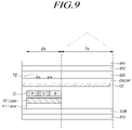
- FIG. 9 is a diagram schematically illustrating a sectional structure of each of the light emitting area EA and the transmissive area TA in the display panel 110 of the transparent touch display device 100 according to embodiments of the present disclosure.
- the light emitting area EA and the transmissive area TA of the subpixel SP may be disposed adjacent to each other.
- Each light emitting area EA may include a TFT (Thin Film Transistor) layer on which transistors DRT and SCT are formed on the substrate SUB, a PE (Pixel Electrode) layer positioned on the TFT Layer, and a light emitting layer EL positioned on the PE layer.
- a common electrode CE may be disposed on the light emitting layer EL in each light emitting area EA.
- TFT layer, PE layer and light emitting layer EL may exist in the light emitting area EA, and the common electrode CE may exist in both the light emitting area EA and the transmissive area TA.
- the common electrode CE may be a transparent electrode (e.g., a transparent cathode electrode) having a transmittance equal to or greater than a predetermined threshold transmittance.
- the common electrode CE may be an electrode having a transmittance less than the critical transmittance in the light emitting area EA, and may be a transparent electrode having a transmittance greater than or equal to the critical transmittance in the transmissive area TA.
- the touch panel TSP may further include a touch passivation layer PAC overlaying or covering the touch electrodes TE.
- the touch panel TSP may be bonded to the cover layer 930 through the adhesive layer 920 .
- the cover layer 930 may include a cover glass or a cover film.
- a lower anti-reflective film 910 may be further disposed under the substrate SUB, and an upper anti-reflective film 940 may be further disposed on the cover layer 930 .
- all layer configurations disposed in the transmissive area TA may have a transmittance greater than or equal to a predetermined threshold transmittance.
- a polarizing plate may be a structure that is disposed in all areas including the light-emitting area EA and the transmission area TA, and has an anti-reflection effect.
- the display panel 110 of the transparent touch display device 100 may not have a polarizing plate disposed in order to increase the transmittance in the transmissive area TA.
- the transmittance may be improved in the transmissive area TA.
- the polarizing plate having anti-reflection effect is not disposed, in the light emitting area EA, reflection by the sensor metal SM of the touch electrodes EA positioned on the uppermost layer may increase. Due to such an increase in reflection, an image anomaly in which a grid pattern caused by a mesh pattern of the touch electrodes TE is recognized may occur. Such an image anomaly is also referred to as a moiré phenomenon.
- a polarizing plate is not applied, and color filters and a black matrix are disposed on or over the encapsulation layer ENCAP in the light emitting area EA.
- the black matrix may be disposed to overlap the touch electrodes TE. In this case, it is possible to prevent image abnormalities caused by non-application of the polarizing plate, but a process procedure for forming color filters and black matrix must be additionally performed. Therefore, it may cause a problem of increasing the complexity of the manufacturing process.
- embodiments of the present disclosure may provide a method of preventing image anomalies that may occur when a polarizing plate is not applied in order to improve transmittance without going through a complicated process procedure. That is, the embodiments of the present disclosure can improve transmittance, prevent image abnormalities, and prevent process complexity. Accordingly, in some embodiments, the transparent touch display device 100 according to embodiments of the present disclosure has a low-reflective structure of touch sensor components including touch electrodes TE and the like under a structure in which a polarizing plate is not applied.
- a low reflection structure of touch sensor components including touch electrodes and the like will be described in detail.
- FIG. 10 is a sectional view of the touch electrode TE having a low reflection structure in the display panel 110 of the transparent touch display device 100 according to embodiments of the present disclosure.
- the transparent touch display device 100 includes a substrate SUB, a driving transistor DRT on the substrate SUB, a pixel electrode PE, a light emitting layer EL, a common electrode CE, an encapsulation layer ENCAP, and a plurality of touch electrodes TE.
- the substrate SUB may include a display area DA in which an image is displayed and a non-display area NDA positioned outside the display area DA.
- the display area DA may include a plurality of light emitting areas EA and a plurality of transmissive areas TA.
- Each of the plurality of subpixels SP may include the driving transistor DRT, the pixel electrode PE, the light emitting layer EL, and the like.
- the common electrode CE may exist in common with respect to the plurality of subpixels SP.
- the driving transistor DRT may be disposed in each of the plurality of subpixels SP corresponding to the plurality of light emitting areas EA.
- the pixel electrode PE may be disposed in each of the plurality of light emitting areas EA, and may be electrically connected to a source electrode or a drain electrode of the driving transistor DRT disposed in each of the plurality of subpixels SP.
- the light emitting layer EL may be disposed in each of the plurality of light emitting areas EA, and may be disposed on the pixel electrode PE.
- the common electrode CE may be positioned on the light emitting layer EL and may be disposed over a plurality of light emitting areas EA and a plurality of transmissive areas TA.
- the common electrode CE may be a transparent common electrode.
- Each of the plurality of touch electrodes TE basically includes a mesh-type sensor metal SM in which a plurality of openings OA are formed.
- Each of the plurality of touch electrodes TE may further include a sensor light control layer SLCL on the sensor metal SM in order to implement a low reflection structure.
- the sensor metal SM of each touch electrode TE may be a portion corresponding to a practical touch electrode TE. That is, the sensor metal SM may be a part to which a touch driving signal is applied or a part to which a touch sensing signal is sensed.
- the sensor light control layer SLCL of each touch electrode TE may be an additional layer for a low reflection structure.
- the sensor light control layer SLCL of each touch electrode TE like the sensor metal SM, may be a part to which a touch driving signal is applied or a part in which a touch sensing signal is sensed.
- the sensor light control layer SLCL of each of the plurality of touch electrodes TE may include a sensor transmission layer STL located on the sensor metal SM and a sensor auxiliary metal SAM located on the sensor transmission layer STL.
- a part of incident light incident on the upper surface of the sensor auxiliary metal SAM may be reflected from the upper surface of the sensor auxiliary metal SAM.
- Another part of the incident light incident on the upper surface of the sensor auxiliary metal SAM may be reflected from the upper surface of the sensor metal SM after passing through the sensor auxiliary metal SAM and the sensor transmission layer STL.
- a light path difference may occur between the first reflected light reflected from the upper surface of the sensor auxiliary metal SAM and the second reflected light reflected from the upper surface of the sensor metal SM.
- a difference in a light path between the first reflected light reflected from the upper surface of the sensor auxiliary metal SAM and the second reflected light reflected from the upper surface of the sensor metal SM may be an odd multiple of a half wavelength. That is, the phase difference (corresponding to the light path difference) between the first reflected light reflected from the upper surface of the sensor auxiliary metal SAM and the second reflected light reflected from the upper surface of the sensor metal SM may be an odd multiple of the half wavelength.
- the first reflected light reflected from the upper surface of the sensor auxiliary metal SAM and the second reflected light reflected from the upper surface of the sensor metal SM cause destructive interference.
- the reflected light (the second reflected light) is generated from the upper surface of the sensor metal SM of the touch electrode TE
- the reflected light (the second reflected light) from the upper surface of the sensor metal SM may be canceled by the reflected light (the first reflected light) generated from the upper surface of the sensor auxiliary metal SAM added over the sensor metal SM. Accordingly, reflected lights directed toward the viewing surface of the display panel disappears, and an image abnormal phenomenon (e.g., moiré phenomenon) caused by reflection may be prevented.
- the display panel 110 of the transparent touch display device 100 may improve transmittance through non-applying of the polarizing plate and prevent image abnormalities that may occur when the polarizing plate is not applied without going through a complicated process procedure (e.g., color filter and black matrix formation process procedure). That is, the display panel 110 of the transparent touch display device 100 may have an effect of improving transmittance, preventing image abnormalities, and preventing process complexity through a non-applied polarizing plate and a low reflection structure of the touch electrodes.
- a complicated process procedure e.g., color filter and black matrix formation process procedure
- each of the plurality of touch electrodes TE may have a multilayer structure including the sensor metal SM, the sensor transmission layer STL, and the sensor auxiliary metal SAM.
- a low reflection structure may be realized due to the multilayer structure of each of the plurality of touch electrodes TE. In the following, the principle of low reflection by the multilayer structure will be described in more detail.
- Equation 1 the right side (2nd cos ⁇ ) denotes a difference in the optical path between the first reflected light reflected from the upper surface of the sensor auxiliary metal SAM and the second reflected light reflected from the upper surface of the sensor metal SM.
- Equation 1 may mean a conditional expression in which the difference in the optical path between the first reflected light reflected from the upper surface of the sensor auxiliary metal SAM and the second reflected light reflected from the upper surface of the sensor metal SM becomes an odd multiple of the half wavelength.
- the wavelength ⁇ of incident light may be in a wavelength range of visible light.
- the refractive index n of the sensor transmission layer STL, the thickness d 1 of the sensor auxiliary metal SAM, and the thickness d 2 of the sensor transmission layer STL may be design factors.
- the sensor transmission layer STL is ITO (Indium Tin Oxide)
- the refractive index n is about 1.8
- m 0
- the angle ⁇ of incidence 0 degrees
- the wavelength k of the incident light is 550 nm
- the thickness d of the sum of the thickness d 1 of the sensor auxiliary metal SAM and the thickness d 2 of the sensor transmission layer STL may be calculated as 76.4 nm (764 ⁇ ).
- d may be designed to be 52.75 nm to 107 nm (527 ⁇ to 1070 ⁇ ).
- the sensor auxiliary metal SAM may be much thinner than the sensor transmission layer STL.
- the thickness d 2 of the sensor transmission layer STL may be approximately 85% of the sum d of the thickness d 1 of the sensor auxiliary metal SAM and the thickness d 2 of the sensor transmission layer STL
- the thickness d 2 of the sensor transmission layer STL may be designed to be 45 nm to 90 nm (450 ⁇ to 900 ⁇ ).
- the sum d of the thickness d 1 of the sensor auxiliary metal SAM and the thickness d 2 of the sensor transmission layer STL may be smaller than the wavelength ⁇ of incident light (d ⁇ ).
- the thickness d 1 of the sensor auxiliary metal SAM may be smaller than the thickness d 2 of the sensor transmission layer STL (d 1 ⁇ d 2 ).
- the sum d of the thickness d 1 of the sensor auxiliary metal SAM and the thickness d 2 of the sensor transmission layer STL becomes equal to the thickness d 2 of the sensor transmission layer STL, and the light refraction phenomenon in the sensor auxiliary metal SAM can be ignored. Accordingly, it is possible to more efficiently and easily design light control for generating destructive interference between the first reflected light and the second reflected light.
- the sum d of the thickness d 1 of the sensor auxiliary metal SAM and the thickness d 2 of the sensor transmission layer STL may be less than or greater than the wavelength ⁇ of the incident light according to the m value of Equation 1 above.
- the sum d of the thickness d 1 of the sensor auxiliary metal SAM and the thickness d 2 of the sensor transmission layer STL may be designed to be an easy value in consideration of the process.
- Equation 1 may be satisfied. Accordingly, the first reflected light reflected from the upper surface of the sensor auxiliary metal SAM and the second reflected light reflected from the upper surface of the sensor metal SM cause destructive interference, so that an image abnormal phenomenon due to reflection may be prevented.
- the thickness d 1 of the sensor auxiliary metal SAM and the thickness d 2 of the sensor transmission layer STL may be accurately set or the material of the sensor transmission layer STL may be accurately selected so as to prevent image abnormalities.
- the selection of the material of the sensor transmission layer STL may mean determination of the refractive index n.
- the sensor transmission layer STL may include a transparent electrode (transparent metal) or may be a transparent non-metal.
- the sensor auxiliary metal SAM and the sensor metal SM may be electrically connected by the sensor transmission layer STL. Accordingly, the electrical resistance of the touch electrode TE decreases, so that the time constant of the touch sensor configuration including the touch electrode TE may decrease. Accordingly, it is possible to accurately transmit electrical signals (touch driving signals and touch sensing signals) through the configuration of the touch sensor, and the touch sensitivity can be improved.
- the sensor metal SM and the sensor auxiliary metal SAM of each of the plurality of touch electrodes TE may be disposed to avoid the light emitting area EA and the transmissive area TA as much as possible. That is, the sensor metal SM and the sensor auxiliary metal SAM of each of the plurality of touch electrodes TE may be disposed so as not to overlap all or part of the light emitting area EA and the transmissive area TA. Accordingly, it is possible to provide a touch sensing function while preventing a decrease in light emission performance and transmittance as much as possible.
- a plurality of subpixels SP may be formed in an area in which one touch electrode TE is formed. Accordingly, in an area where one touch electrode TE is formed, the transmissive areas TA and the light emitting areas EA of the plurality of subpixels SP may exist.
- the plurality of openings OA formed in each of the plurality of touch electrodes TE may be positioned to correspond to the plurality of light emitting areas EA and the plurality of transmissive areas TA. Accordingly, high transmission performance can be provided, and high light emission performance can be provided even if the touch electrodes TE are disposed between the light emitting device ED and the viewing surface.
- FIGS. 11 and 12 are sectional views of an area where a first bridge electrode BE 1 and a second bridge electrode BE 2 intersect in the display panel 110 of the transparent touch display device 100 according to embodiments of the present disclosure.
- the first touch electrode TE 1 and the second touch electrode TE 2 are disposed adjacent to each other in the second direction, and may be electrically connected to each other by the first bridge electrode BE 1 .
- the third touch electrode TE 3 and the fourth touch electrode TE 4 are disposed adjacent to each other in the first direction and may be electrically connected by the second bridge electrode BE 2 .
- the second bridge electrode BE 2 may be disposed to cross the first bridge electrode BE 1 and partially overlap the first bridge electrode BE 1 .
- the first bridge electrode BE 1 may be positioned on a different layer from the first touch electrode TE 1 and the second touch electrode TE 2 .
- the second bridge electrode BE 2 may be located on the same layer as the first touch electrode TE 1 and the second touch electrode TE 2 .
- the second bridge electrode BE 2 may be integrally formed with the third touch electrode TE 3 and the fourth touch electrode TE 4 .
- the first bridge electrode BE 1 may include a first bridge metal BM 1 .
- the first bridge metal BM 1 may be positioned on a different layer from the first touch electrode TE 1 and the second touch electrode TE 2 with the interlayer insulating layer ILD interposed therebetween.
- a part of the first bridge metal BM 1 may be electrically connected to the sensor metal SM of the first touch electrode TE 1 through the first contact hole of the interlayer insulating layer ILD.
- Another part of the first bridge metal BM 1 may be electrically connected to the sensor metal SM of the second touch electrode TE 2 through the second contact hole of the interlayer insulating layer ILD.
- the second bridge electrode BE 2 may be integrally formed with the third and fourth touch electrodes TE 3 and TE 4 .
- the second bridge electrode BE 2 may have the same multilayer structure as the third and fourth touch electrodes TE 3 and TE 4 .
- Each of the first to fourth touch electrodes TE 1 to TE 4 may include a sensor metal SM and a sensor light control layer SLCL on the sensor metal SM.
- the sensor light control layer SLCL may include a sensor transmission layer STL disposed on the sensor metal SM and a sensor auxiliary metal SAM disposed on the sensor transmission layer STL.
- the second bridge electrode BE 2 may include a second bridge metal BM 2 and a second bridge light control layer BLCL 2 positioned on the second bridge metal BM 2 .
- the second bridge light control layer BLCL 2 of the second bridge electrode BE 2 may include a second bridge transmission layer BTL 2 on the second bridge metal BM 2 , and a second bridge auxiliary metal BAM 2 on the second bridge transmission layer BTL 2 .
- the second bridge electrode BE 2 may include a second bridge metal BM 2 , a second bridge transmission layer BTL 2 on the second bridge metal BM 2 , and a second bridge auxiliary metal BAM 2 on the second bridge transmission layer BTL 2 .
- the second bridge metal BM 2 may be integrally formed with the sensor metal SM of each of the third and fourth touch electrodes TE 3 and TE 4 .
- the second bridge transmission layer BTL 2 may be integrally formed with the sensor transmission layer STL of each of the third and fourth touch electrodes TE 3 and TE 4 .
- the second bridge auxiliary metal BAM 2 may be integrally formed with the sensor auxiliary metal SAM of each of the third and fourth touch electrodes TE 3 and TE 4 .
- the second bridge metal BM 2 may include the same material as the sensor metal SM of each of the third and fourth touch electrodes TE 3 and TE 4 .
- the second bridge metal BM 2 may be formed to have the same thickness as the sensor metal SM of each of the third and fourth touch electrodes TE 3 and TE 4 .
- the second bridge transmission layer BTL 2 may include the same material as the sensor transmission layer STL of each of the third and fourth touch electrodes TE 3 and TE 4 .
- the second bridge transmission layer BTL 2 may be formed to have the same thickness as the sensor transmission layer STL of each of the third and fourth touch electrodes TE 3 and TE 4 .
- the second bridge auxiliary metal BAM 2 may include the same material as the sensor auxiliary metal SAM of each of the third and fourth touch electrodes TE 3 and TE 4 .
- the second bridge auxiliary metal BAM 2 may be formed to have the same thickness as the sensor auxiliary metal SAM of each of the third and fourth touch electrodes TE 3 and TE 4 .
- the second bridge electrode BE 2 may have the same multilayer structure as the touch electrode TE. Accordingly, the second bridge electrode BE 2 , like the touch electrode TE, has a low-reflective structure, and an image abnormal phenomenon caused by the second bridge electrode BE 2 can be prevented.
- the second bridge electrode BE 2 may overlap a part of the first bridge electrode BE 1 with the interlayer insulating layer ILD interposed therebetween, and may be electrically separated from the first bridge electrode BE 1 by the interlayer insulating layer ILD.
- the first bridge electrode BE 1 may have a single layer structure composed of the first bridge metal BM 1 . Accordingly, the interlayer insulating layer ILD may be positioned between the first bridge metal BM 1 of the first bridge electrode BE 1 and the second bridge metal BM 2 of the second bridge electrode BE 2 .
- the first bridge electrode BE 1 may be formed in a single layer structure. Accordingly, there is an advantage in that the first bridge electrode BE 1 can be easily formed.
- the first bridge electrode BE 1 may have a multilayer structure, similar to the second bridge electrode BE 2 .
- the first bridge electrode BE 1 may further include a first bridge light control layer BLCL 1 positioned on the first bridge metal BM 1 .
- the first bridge light control layer BLCL 1 may include a first bridge transmission layer BTL 1 on the first bridge metal BM 1 and a first bridge auxiliary metal BAM 1 on the first bridge transmission layer BTL 1 .
- the first bridge metal BM 1 may include the same material as the sensor metal SM of each of the first and second touch electrodes TE 1 and TE 2 .
- the first bridge metal BM 1 may have a thickness corresponding to the sensor metal SM of each of the first and second touch electrodes TE 1 and TE 2 .
- the first bridge transmission layer BTL 1 may include the same material as the sensor transmission layer STL of each of the first and second touch electrodes TE 1 and TE 2 .
- the first bridge transmission layer BTL 1 may have a thickness corresponding to the sensor transmission layer STL of each of the first and second touch electrodes TE 1 and TE 2 .
- the first bridge auxiliary metal BAM 1 may include the same material as the sensor auxiliary metal SAM of each of the first and second touch electrodes TE 1 and TE 2 .
- the first bridge auxiliary metal BAM 1 may have a thickness corresponding to the sensor auxiliary metal SAM of each of the first and second touch electrodes TE 1 and TE 2 .
- the first bridge electrode BE 1 may have the same multilayer structure as the touch electrode TE. Accordingly, like the touch electrode TE, the first bridge electrode BE 1 has a low reflection structure, and an image abnormal phenomenon caused by the first bridge electrode BE 1 can be prevented.
- the first bridge electrode BE 1 has a multilayer structure. Accordingly, the interlayer insulating layer ILD may be positioned between the first bridge auxiliary metal BAM 1 of the first bridge electrode BE 1 and the second bridge metal BM 2 of the second bridge electrode BE 2 .
- the first bridge metal BM 1 of the first bridge electrode BE 1 and the second bridge metal BM 2 of the second bridge electrode BE 2 are portions electrically connected to the sensor metal SM of the touch electrode TE. Accordingly, the first bridge metal BM 1 of the first bridge electrode BE 1 and the second bridge metal BM 2 of the second bridge electrode BE 2 may be a portion to which a touch driving signal is applied or a touch sensing signal is sensed.
- the first bridge light control layer BLCL 1 of the first bridge electrode BE 1 and/or the second bridge light control layer BLCL 2 of the second bridge electrode BE 2 may be an additional layer for a low reflection structure.
- the first bridge light control layer BLCL 1 of the first bridge electrode BE 1 and/or the second bridge light control layer BLCL 2 of the second bridge electrode BE 2 may be a portion to which a touch driving signal is applied or a touch sensing signal is sensed.
- FIG. 13 is a sectional view of the display panel 110 of the transparent touch display device 100 according to embodiments of the present disclosure, and is a sectional view of the display panel 110 to which the touch electrode TE having the low reflection structure is applied.
- the sectional structure of FIG. 13 is almost the same as the sectional structure of FIG. 7 , and differs from the sectional structure of FIG. 7 only in the low-reflective structure of the touch electrode TE. In the following, features that are different from the sectional structure of FIG. 7 will be mainly described.
- the transparent touch display device 100 further comprise a dam unit DAM located in an area where the outer inclined surface SLP of the encapsulation layer ENCAP ends, a touch pad unit TP located in the non-display area NDA and further outside the dam unit DAM, and a touch routing wiring Y-TRW electrically connecting some of the touch electrodes TE 1 and TE 2 among the plurality of touch electrodes TE and the touch pad unit TP.
- a dam unit DAM located in an area where the outer inclined surface SLP of the encapsulation layer ENCAP ends
- a touch pad unit TP located in the non-display area NDA and further outside the dam unit DAM
- a touch routing wiring Y-TRW electrically connecting some of the touch electrodes TE 1 and TE 2 among the plurality of touch electrodes TE and the touch pad unit TP.
- the touch routing wiring Y-TRW may descend along an outer inclined surface SLP of the encapsulation layer ENCAP and pass over the dam unit DAM to be electrically connected to the touch pad unit TP.
- the touch routing wiring Y-TRW may have a single layer structure.
- the touch routing wiring Y-TRW may include a wiring metal WM.
- the touch routing wiring Y-TRW may have a multilayer structure to which a low reflection structure is applied.
- the touch routing wiring Y-TRW may further include a wiring metal WM and a wiring light control layer WLCL positioned on the wiring metal WM.
- the wiring metal WM of the touch routing wiring Y-TRW may be a portion electrically connected to the sensor metal SM of the touch electrode TE. Accordingly, the wiring metal WM of the touch routing wiring Y-TRW may be a portion to which a touch driving signal is applied or a touch sensing signal is sensed.
- the wiring light control layer WLCL of the touch routing wiring Y-TRW may be an additional layer for a low reflection structure.
- the wiring light control layer WLCL of the touch routing wiring Y-TRW may be a portion to which a touch driving signal is applied or a touch sensing signal is sensed.
- the wiring light control layer WLCL of the touch routing wiring Y-TRW may include a wiring transmission layer WTL located on the wiring metal WM and a wiring auxiliary metal WAM located on the wiring transmission layer WTL.
- the wiring metal WM of the touch routing wiring Y-TRW and the sensor metal SM of the touch electrodes TE 1 and TE 2 may include the same material.
- the wiring metal WM of the touch routing wiring Y-TRW and the sensor metal SM of the touch electrodes TE 1 and TE 2 may have corresponding thicknesses.
- the wiring auxiliary metal WAM of the touch routing wiring Y-TRW and the sensor auxiliary metal SAM of the touch electrodes TE 1 and TE 2 may include the same material.
- the wiring auxiliary metal WAM of the touch routing wiring Y-TRW and the sensor auxiliary metal SAM of the touch electrodes TE 1 and TE 2 may have corresponding thicknesses.
- the wiring transmission layer WTL of the touch routing wiring Y-TRW and the sensor transmission layer STL of the touch electrodes TE 1 and TE 2 may include the same material.
- the wiring transmission layer WTL of the touch routing wiring Y-TRW and the sensor transmission layer STL of the touch electrodes TE 1 and TE 2 may have corresponding thicknesses.
- the touch routing wiring Y-TRW has a low reflection structure, so that an image abnormal phenomenon caused by the touch routing wiring Y-TRW can be prevented.
- the touch routing wiring Y-TRW may have an extended second touch electrode TE 2 .
- FIG. 14 is a plan view showing mesh pattern structure of first to fourth touch electrodes TE 1 to TE 4 having the low reflection structure, when the arrangement structure of FIG. 2 is applied in the display panel 110 of the transparent touch display device 100 according to embodiments of the present disclosure.
- FIG. 15 is an enlarged plan view of a partial area 1700 of FIG. 14 .
- the first and second touch electrodes TE 1 and TE 2 are disposed adjacent to each other in a second direction (e.g., column direction, y-axis direction), and may be electrically connected to each other by one or more first bridge electrodes BE 1 .
- the third and fourth touch electrodes TE 3 and TE 4 are disposed adjacent to each other in the first direction (e.g., row direction, x-axis direction), and may be electrically connected to each other by one or more second bridge electrodes BE 2 .
- the first and second touch electrodes TE 1 and TE 2 adjacent in the second direction may be Y-touch electrodes Y-TE adjacent in the y-axis direction.
- the third and fourth touch electrodes TE 3 and TE 4 adjacent in the first direction may be X-touch electrodes X-TE adjacent in the x-axis direction.
- first bridge electrode BE 1 and the second bridge electrode BE 2 may cross each other.
- the first bridge electrode BE 1 may be positioned on a different layer from the first and second touch electrodes TE 1 and TE.
- the second bridge electrode BE 2 may be located on the same layer as the third and fourth touch electrodes TE 3 and TE 4 , and may be integrally formed with the third and fourth touch electrodes TE 3 and TE 4 . That is, the first bridge electrode BE 1 may be positioned on a different layer from the first to fourth touch electrodes TE 1 to TE 4 .
- the second bridge electrode BE 2 may be positioned on the same layer as the first to fourth touch electrodes TE 1 to TE 4 .
- each of the first to fourth touch electrodes TE 1 to TE 4 may be formed in a multilayer structure including a sensor metal SM patterned in a mesh type and a sensor light control layer SLCL in order to realize a low reflection structure.
- the sensor light control layer SLCL may include a sensor transmission layer STL positioned on the sensor metal SM and a sensor auxiliary metal SAM positioned on the sensor transmission layer STL.
- the touch driving circuit 160 may supply a touch driving signal to at least one of the plurality of driving touch electrode lines (e.g., X-TEL or Y-TEL) and sense at least one of the plurality of sensing touch electrode lines (e.g., Y-TEL or X-TEL).
- the plurality of driving touch electrode lines e.g., X-TEL or Y-TEL
- sense at least one of the plurality of sensing touch electrode lines e.g., Y-TEL or X-TEL.
- Each of the plurality of driving touch electrode lines may be an assembly of two or more touch electrodes TE disposed adjacent to each other in a first direction or a second direction and electrically connected to each other.
- Each of the plurality of sensing touch electrode lines may be an assembly of two or more touch electrodes TE disposed adjacent to each other in a second direction or a first direction and electrically connected to each other.
- the first and second touch electrodes TE 1 and TE 2 electrically connected by the first bridge electrode BE 1 may constitute one driving touch electrode line (e.g., X-TEL or Y-TEL).
- the third and fourth touch electrodes TE 3 and TE 4 electrically connected by the second bridge electrode BE 2 may constitute one sensing touch electrode line (e.g., Y-TEL or X-TEL).
- first and second touch electrodes TE 1 and TE 2 electrically connected by the first bridge electrode BE 1 may constitute one sensing touch electrode line (e.g., Y-TEL or X-TEL).
- the third and fourth touch electrodes TE 3 and TE 4 electrically connected by the second bridge electrode BE 2 may constitute one driving touch electrode line (e.g., X-TEL or Y-TEL).
- mesh patterns of the first to fourth touch electrodes TE 1 to TE 4 may be disposed to avoid the light emitting areas EA and the transmissive areas TA as much as possible. That is, the multilayer structure of each of the first to fourth touch electrodes TE 1 to TE 4 may be disposed so as to avoid the light emitting areas EA and the transmissive areas TA as much as possible.
- the multilayer structure may include a sensor metal SM, a sensor transmission layer STL, and a sensor auxiliary metal SAM.
- the multilayer structure of each of the plurality of touch electrodes TE may be disposed so as not to overlap all or part of the light emitting areas EA and the transmissive areas TA.
- each of the plurality of touch electrodes TE may be arranged so that overlapping is reduced or minimized even when overlapping with at least one of the light emitting areas EA and the transmissive areas TA. Accordingly, it is possible to provide a touch sensing function while preventing a decrease in light emission performance and transmittance as much as possible.
- the shape of the mesh pattern of the first to fourth touch electrodes TE 1 to TE 4 in the planar structure of FIG. 14 may be different from the shape of the mesh pattern of the first to fourth touch electrodes TE 1 to TE 4 in FIG. 8 .
- the shape of the mesh pattern of the first to fourth touch electrodes TE 1 to TE 4 may vary according to the arrangement structure of the light emitting areas EA and the transmissive areas TA.
- the shape of the mesh pattern of the first to fourth touch electrodes TE 1 to TE 4 illustrated in FIG. 14 is suitable for the arrangement structure of the light emitting areas (EA 1 , EA 2 , EA 3 , EA 4 , EA 5 , EA 6 ) and the transmissive areas (TA 1 , TA 2 ) of FIG. 15 .
- an area occupied by each of the first to fourth touch electrodes TE 1 to TE 4 among the plurality of touch electrodes TE may include a plurality of light emitting areas EA 1 to EA 6 and a plurality of transmissive areas TA 1 and TA 2 .
- a plurality of openings OA formed in each of the first to fourth touch electrodes TE 1 to TE 4 among the plurality of touch electrodes TE may include a plurality of first openings OA 1 corresponding to the plurality of light emitting areas EA (EA 1 ⁇ EA 6 ) and a plurality of second openings OA 2 corresponding to the plurality of transparent areas TA (TA 1 , TA 2 ).
- the mesh patterns SM, STL, and SAM of each of the first to fourth touch electrodes TE 1 to TE 4 may be disposed to avoid the light emitting areas EA (EA 1 ⁇ EA 6 ) and the transmissive areas TA (TA 1 , TA 2 ) as much as possible. Therefore, the luminous efficiency and transmittance can be significantly improved.
- the first opening OA 1 may have a shape such as a rectangle, a hexagon, an oval, and a circle.
- the second opening OA 2 may have a shape such as an octagon, an oval, and a circle.
- a plurality of first openings OA 1 may correspond to first to third light emitting areas EA 1 to EA 3 .
- the first to third light emitting areas EA 1 to EA 3 may be included in the i-th light emitting area row (i-th EA Row) and may be disposed adjacent to each other in the first direction (e.g., row direction).
- the first opening OA 1 may correspond to fourth to sixth light emitting areas EA 4 to EA 6 .
- the fourth to sixth light emitting areas EA 4 to EA 6 may be included in the (i+1)-th light emitting area row ((i+1)-th EA Row) and may be disposed adjacent to each other in the first direction (e.g., row direction).
- the fourth to sixth light emitting areas EA 4 to EA 6 may be disposed adjacent to the first to third light emitting areas EA 1 to EA 3 in a second direction (e.g., column direction) crossing the first direction, respectively.
- the plurality of second openings OA 2 may correspond to the first transmissive area TA 1 and the second transmissive area TA 2 .
- the first transmissive area TA 1 may be located between the first light emitting area EA 1 in the i-th light emitting area row (i-th EA Row) and the fourth light emitting area EA 4 in the (i+1)-th light emitting area row ((i+1)-th EA Row).
- the second transmissive area TA 2 may be positioned between the third light emitting area EA 3 in the i-th light emitting area row (i-th EA Row) and the sixth light emitting area EA 6 in the (i+1)-th light emitting area row ((i+1)-th EA Row).
- the first transmissive area TA 1 may be extended to a partial space in a space between the second emission area EA 2 and the fifth emission area EA 5 .
- the second transmissive area TA 2 may extend to another partial space in the space between the second emission area EA 2 and the fifth emission area EA 5 .
- the sensor auxiliary metal SAM, the sensor transmission layer STL, and the sensor metal SM included in the first touch electrode TE 1 may be located between adjacent areas among the first to sixth light emitting areas EA 1 to EA 6 and the first and second transmissive areas TA 1 and TA 2 .
- the first light emitting area EA 1 , the third light emitting area EA 3 , the fourth light emitting area EA 4 , and the sixth light emitting area EA 6 may be light emitting areas (first color light emitting areas) of the first color subpixel (e.g., Red SP).
- the second light emitting area EA 2 may be a light emitting area (second color light emitting area) of a second color subpixel (e.g., Green SP).
- the fifth light emitting area EA 5 may be a light emitting area (third color light emitting area) of a third color subpixel (e.g., Blue SP).
- the sizes of the first light emitting area EA 1 , the third light emitting area EA 3 , the fourth light emitting area EA 4 , and the sixth light emitting area EA 6 may correspond to each other.
- the sizes of the second light emitting area EA 2 and the fifth light emitting area EA 5 may correspond to each other.
- the size of each of the second and fifth light emitting areas EA 2 and EA 5 may be larger than the size of each of the first light emitting area EA 1 , the third light emitting area EA 3 , the fourth light emitting area EA 4 , and the sixth light emitting area EA 6 .
- the sizes of the first transmissive area TA 1 and the second transmissive area TA 2 may correspond to each other.
- the sizes of each of the first and second transmissive areas TA 1 and TA 2 may be larger than the size of each of the second and fifth light emitting areas EA 2 and EA 5 . Accordingly, the transmittance can be improved.
- the low reflection structure of the touch electrode TE can be effectively applied.
- FIG. 16 is plan views showing mesh pattern structure of the touch electrode TE having the low reflection structure, when the arrangement structure of FIG. 3 is applied in the display panel 110 of the transparent touch display device 100 according to embodiments of the present disclosure.
- FIG. 17 is plan views showing mesh pattern structure of the touch electrode TE having the low reflection structure, when the arrangement structure of FIG. 4 is applied in the display panel 110 of the transparent touch display device 100 according to embodiments of the present disclosure.
- the mesh patterns SM, STL, and SAM of the first touch electrode TE 1 among the plurality of touch electrodes TE may be disposed while avoiding the light emitting areas (EA 1 , EA 2 , EA 3 ) and the transmissive areas (TA 1 , TA 2 , TA 3 ) as much as possible.
- the plurality of openings OA formed in the first touch electrode TE 1 may correspond to a plurality of light emitting areas (EA 1 , EA 2 , and EA 3 ). And the plurality of openings OA formed in the first touch electrode TE 1 may further correspond to a plurality of transmissive areas (TA 1 , TA 2 , and TA 3 ) or one or more transmissive areas (One or more transmissive areas to which TA 1 , TA 2 , and TA 3 are combined). Accordingly, luminous efficiency and transmittance can be significantly improved.
- a plurality of transmissive areas may include the first to third transmissive areas TA 1 to TA 3 .
- the first to third transmissive areas TA 1 to TA 3 may all be separate types, or two or more of the first to third transmissive areas TA 1 to TA 3 may be connected.
- the plurality of light emitting areas may include first light emitting area EA 1 , a second light emitting area EA 2 , and a third light emitting area EA 3 adjacent to each other in a first direction.
- the plurality of the transmissive areas may include the first transmissive area TA 1 , the second transmissive area TA 2 , and the third transmissive area TA 3 adjacent to each other in a first direction.
- the first to third transmissive areas TA 1 to TA 3 are disposed adjacent to the first to third light emitting areas EA 1 to EA 3 in a second direction.
- the sensor auxiliary metal SAM, the sensor transmission layer STL, and the sensor metal SM included in the first touch electrode TE 1 may be located between adjacent areas among the first to third light emitting areas EA 1 to EA 3 and the first to third transmissive area TA 1 to TA 3 , or may be disposed to at least partially surround the first to third light emitting areas EA 1 to EA 3 and the first to third transmissive area TA 1 to TA 3 .
- the mesh patterns SM, STL, and SAM of the first touch electrode TE 1 among the plurality of touch electrodes TE may be disposed while avoiding the light emitting areas EA 1 to EA 3 and the transmissive areas TA 1 to TA 3 as much as possible. Accordingly, luminous efficiency and transmittance can be significantly improved.
- the mesh patterns SM, STL, and SAM of the first touch electrode TE 1 among the plurality of touch electrodes TE may be disposed while avoiding the light emitting areas EA 1 to EA 4 and the transmissive areas TA 1 to TA 4 as much as possible.
- a plurality of openings OA formed in the first touch electrode TE 1 may correspond to a plurality of light emitting areas EA 1 to EA 4 and a plurality of transmissive areas TA 1 to TA 4 . Accordingly, luminous efficiency and transmittance can be significantly improved.
- the plurality of light emitting areas EA 1 to EA 4 may include a first light emitting area EA 1 , a second light emitting area EA 2 , a third light emitting area EA 3 , and a fourth light emitting area EA 4 adjacent to each other in a second direction.
- the plurality of transmissive areas TA 1 to TA 4 may include a first transmissive area TA 1 , a second transmissive area TA 2 , a third transmissive area TA 3 , and a fourth transmissive area TA 4 adjacent to each other in a second direction.
- the first to fourth transmissive areas TA 1 to TA 4 may be disposed adjacent to the first to fourth light emitting areas EA 1 to EA 4 in a first direction.
- the sensor auxiliary metal SAM, the sensor transmissive layer STL, and the sensor metal SM included in the first touch electrode TE 1 may be positioned between adjacent areas among the first to fourth light emitting areas EA 1 to EA 4 and the first to fourth transmissive areas TA 1 to TA 4 , or may be disposed to at least partially surround the first to fourth light emitting areas EA 1 to EA 4 and the first to fourth transmissive areas TA 1 to TA 4 . Accordingly, the mesh patterns SM, STL, and SAM of the first touch electrode TE 1 among the plurality of touch electrodes TE may be disposed while avoiding the light emitting areas EA 1 to EA 4 and the transmissive areas TA 1 to TA 4 as much as possible. Accordingly, luminous efficiency and transmittance can be significantly improved.
- the low-reflection structure of the touch electrode TE can be effectively applied.
- the transparent touch display device 100 has been described as an organic light emitting display device.
- the low-reflection structure of the touch sensor configuration which is the main feature of the present disclosure, may be equally applied even when the transparent touch display device 100 is a display type (e.g., liquid crystal display device, etc.) other than an organic light-emitting display device.
- the transparent touch display device 100 according to embodiments of the present disclosure will be briefly described again.
- the transparent touch display device 100 may include: a display panel 110 including a plurality of data lines DL, a plurality of gate lines GL, and a plurality of touch electrodes TE; a data driving circuit 120 for driving a plurality of data lines; a gate driving circuit 130 for driving a plurality of gate lines; and a touch driving circuit 160 driving a plurality of touch electrodes TE.
- the display panel 110 may include a display area DA in which an image is displayed and a non-display area NDA positioned outside the display area DA.
- the display area DA may include a plurality of light emitting areas EA and a plurality of transmissive areas TA.
- Each of the plurality of touch electrodes TE may include: a mesh-type sensor metal SM in which a plurality of openings OA are formed; a sensor transmission layer STL positioned on the sensor metal SM; and a sensor auxiliary metal SAM positioned on the sensor transmission layer STL.
- Part of the incident light incident on the upper surface of the sensor auxiliary metal SAM may be reflected from the upper surface of the sensor auxiliary metal SAM.
- Another part of the incident light incident on the upper surface of the sensor auxiliary metal SAM may be reflected from the upper surface of the sensor metal SM after passing through the sensor auxiliary metal SAM and the sensor transmission layer STL.
- the reflected light reflected from the upper surface of the sensor auxiliary metal SAM and the reflected light reflected from the upper surface of the sensor metal SM may have a light path difference and a phase difference corresponding to an odd multiple of a half wavelength of the incident light.
- the reflected light reflected from the upper surface of the sensor auxiliary metal SAM and the reflected light reflected from the upper surface of the sensor metal SM may cause destructive interference. Accordingly, an image abnormal phenomenon due to reflection from the touch electrode TE can be prevented.
Landscapes
- Engineering & Computer Science (AREA)
- General Engineering & Computer Science (AREA)
- Theoretical Computer Science (AREA)
- Physics & Mathematics (AREA)
- Human Computer Interaction (AREA)
- General Physics & Mathematics (AREA)
- Microelectronics & Electronic Packaging (AREA)
- Optics & Photonics (AREA)
- Devices For Indicating Variable Information By Combining Individual Elements (AREA)
- Electroluminescent Light Sources (AREA)
Abstract
Description
Claims (16)
Applications Claiming Priority (2)
| Application Number | Priority Date | Filing Date | Title |
|---|---|---|---|
| KR1020200075297A KR20210157239A (en) | 2020-06-19 | 2020-06-19 | Transparent touch display device |
| KR10-2020-0075297 | 2020-06-19 |
Publications (2)
| Publication Number | Publication Date |
|---|---|
| US20210397305A1 US20210397305A1 (en) | 2021-12-23 |
| US11513650B2 true US11513650B2 (en) | 2022-11-29 |
Family
ID=78923884
Family Applications (1)
| Application Number | Title | Priority Date | Filing Date |
|---|---|---|---|
| US17/319,976 Active US11513650B2 (en) | 2020-06-19 | 2021-05-13 | Transparent touch display device |
Country Status (3)
| Country | Link |
|---|---|
| US (1) | US11513650B2 (en) |
| KR (1) | KR20210157239A (en) |
| CN (1) | CN113821118B (en) |
Families Citing this family (4)
| Publication number | Priority date | Publication date | Assignee | Title |
|---|---|---|---|---|
| KR102946345B1 (en) * | 2020-09-16 | 2026-03-31 | 삼성디스플레이 주식회사 | Display device |
| US12004379B2 (en) * | 2020-11-30 | 2024-06-04 | Lg Display Co., Ltd. | Display device |
| KR20230102583A (en) | 2021-12-30 | 2023-07-07 | 엘지디스플레이 주식회사 | Touch Display Apparatus |
| KR20240029598A (en) * | 2022-08-25 | 2024-03-06 | 삼성디스플레이 주식회사 | Display device |
Citations (2)
| Publication number | Priority date | Publication date | Assignee | Title |
|---|---|---|---|---|
| US20180182817A1 (en) * | 2016-12-28 | 2018-06-28 | Lg Display Co., Ltd. | Display device |
| US20180182816A1 (en) * | 2016-12-26 | 2018-06-28 | Lg Display Co., Ltd. | Display Device with Integrated Touch Screen |
Family Cites Families (5)
| Publication number | Priority date | Publication date | Assignee | Title |
|---|---|---|---|---|
| KR102793060B1 (en) * | 2016-12-16 | 2025-04-08 | 엘지디스플레이 주식회사 | Display device and fabricating method thereof |
| KR102402690B1 (en) * | 2017-06-01 | 2022-05-26 | 엘지디스플레이 주식회사 | Touch display device and panel |
| US10452201B1 (en) * | 2018-03-30 | 2019-10-22 | Sharp Kabushiki Kaisha | Touch sensor for display with shield |
| US10845902B2 (en) * | 2018-03-30 | 2020-11-24 | Sharp Kabushiki Kaisha | Touch sensor for display |
| KR102463801B1 (en) * | 2018-04-03 | 2022-11-03 | 엘지디스플레이 주식회사 | Touch display device and touch sensing method |
-
2020
- 2020-06-19 KR KR1020200075297A patent/KR20210157239A/en active Pending
-
2021
- 2021-05-13 US US17/319,976 patent/US11513650B2/en active Active
- 2021-06-11 CN CN202110657121.3A patent/CN113821118B/en active Active
Patent Citations (2)
| Publication number | Priority date | Publication date | Assignee | Title |
|---|---|---|---|---|
| US20180182816A1 (en) * | 2016-12-26 | 2018-06-28 | Lg Display Co., Ltd. | Display Device with Integrated Touch Screen |
| US20180182817A1 (en) * | 2016-12-28 | 2018-06-28 | Lg Display Co., Ltd. | Display device |
Also Published As
| Publication number | Publication date |
|---|---|
| KR20210157239A (en) | 2021-12-28 |
| US20210397305A1 (en) | 2021-12-23 |
| CN113821118A (en) | 2021-12-21 |
| CN113821118B (en) | 2024-03-29 |
Similar Documents
| Publication | Publication Date | Title |
|---|---|---|
| JP7523507B2 (en) | Touch Display Device | |
| US10908758B2 (en) | Touch display device and touch sensing method | |
| JP7743553B2 (en) | Display Device | |
| US10996806B2 (en) | Touch display device | |
| JP6986601B2 (en) | Touch display device | |
| JP7005566B2 (en) | Touch panel and touch display device | |
| US10802634B2 (en) | Touch display panel and touch display device | |
| US10795480B2 (en) | Touch display device and touch sensing method | |
| US11513650B2 (en) | Transparent touch display device | |
| KR20210037299A (en) | Touch display device | |
| CN112286406B (en) | touch display device | |
| CN112286404B (en) | Touch display device | |
| CN112445367B (en) | Touch display device | |
| US11307709B2 (en) | Touch driving circuit and touch display device for reducing noise of touch sensing signal according to display driving | |
| KR20220073296A (en) | Touch display device | |
| CN115586843A (en) | touch display device | |
| US11861125B2 (en) | Transparent touch display device | |
| KR20230100485A (en) | Display panel and display device comprising the same | |
| KR20230082149A (en) | Display panel and display device |
Legal Events
| Date | Code | Title | Description |
|---|---|---|---|
| FEPP | Fee payment procedure |
Free format text: ENTITY STATUS SET TO UNDISCOUNTED (ORIGINAL EVENT CODE: BIG.); ENTITY STATUS OF PATENT OWNER: LARGE ENTITY |
|
| AS | Assignment |
Owner name: LG DISPLAY CO., LTD., KOREA, REPUBLIC OF Free format text: ASSIGNMENT OF ASSIGNORS INTEREST;ASSIGNORS:CHO, NAMWOOK;KIM, EUITAE;SHIN, KISEOB;AND OTHERS;SIGNING DATES FROM 20210430 TO 20210511;REEL/FRAME:056374/0290 |
|
| STPP | Information on status: patent application and granting procedure in general |
Free format text: DOCKETED NEW CASE - READY FOR EXAMINATION |
|
| STPP | Information on status: patent application and granting procedure in general |
Free format text: NON FINAL ACTION MAILED |
|
| STPP | Information on status: patent application and granting procedure in general |
Free format text: RESPONSE TO NON-FINAL OFFICE ACTION ENTERED AND FORWARDED TO EXAMINER |
|
| STPP | Information on status: patent application and granting procedure in general |
Free format text: NOTICE OF ALLOWANCE MAILED -- APPLICATION RECEIVED IN OFFICE OF PUBLICATIONS |
|
| STPP | Information on status: patent application and granting procedure in general |
Free format text: PUBLICATIONS -- ISSUE FEE PAYMENT VERIFIED |
|
| STCF | Information on status: patent grant |
Free format text: PATENTED CASE |
|
| MAFP | Maintenance fee payment |
Free format text: PAYMENT OF MAINTENANCE FEE, 4TH YEAR, LARGE ENTITY (ORIGINAL EVENT CODE: M1551); ENTITY STATUS OF PATENT OWNER: LARGE ENTITY Year of fee payment: 4 |