US11509303B2 - Glitch power analysis and optimization engine - Google Patents
Glitch power analysis and optimization engine Download PDFInfo
- Publication number
- US11509303B2 US11509303B2 US16/915,099 US202016915099A US11509303B2 US 11509303 B2 US11509303 B2 US 11509303B2 US 202016915099 A US202016915099 A US 202016915099A US 11509303 B2 US11509303 B2 US 11509303B2
- Authority
- US
- United States
- Prior art keywords
- glitch
- pins
- bottleneck
- total
- power
- Prior art date
- Legal status (The legal status is an assumption and is not a legal conclusion. Google has not performed a legal analysis and makes no representation as to the accuracy of the status listed.)
- Active, expires
Links
Images


Classifications
-
- H—ELECTRICITY
- H03—ELECTRONIC CIRCUITRY
- H03K—PULSE TECHNIQUE
- H03K17/00—Electronic switching or gating, i.e. not by contact-making and –breaking
- H03K17/51—Electronic switching or gating, i.e. not by contact-making and –breaking characterised by the components used
- H03K17/56—Electronic switching or gating, i.e. not by contact-making and –breaking characterised by the components used by the use, as active elements, of semiconductor devices
- H03K17/687—Electronic switching or gating, i.e. not by contact-making and –breaking characterised by the components used by the use, as active elements, of semiconductor devices the devices being field-effect transistors
-
- G—PHYSICS
- G06—COMPUTING; CALCULATING OR COUNTING
- G06F—ELECTRIC DIGITAL DATA PROCESSING
- G06F30/00—Computer-aided design [CAD]
- G06F30/30—Circuit design
- G06F30/32—Circuit design at the digital level
- G06F30/33—Design verification, e.g. functional simulation or model checking
- G06F30/3308—Design verification, e.g. functional simulation or model checking using simulation
-
- G—PHYSICS
- G01—MEASURING; TESTING
- G01R—MEASURING ELECTRIC VARIABLES; MEASURING MAGNETIC VARIABLES
- G01R31/00—Arrangements for testing electric properties; Arrangements for locating electric faults; Arrangements for electrical testing characterised by what is being tested not provided for elsewhere
- G01R31/28—Testing of electronic circuits, e.g. by signal tracer
- G01R31/317—Testing of digital circuits
- G01R31/31708—Analysis of signal quality
-
- G—PHYSICS
- G01—MEASURING; TESTING
- G01R—MEASURING ELECTRIC VARIABLES; MEASURING MAGNETIC VARIABLES
- G01R31/00—Arrangements for testing electric properties; Arrangements for locating electric faults; Arrangements for electrical testing characterised by what is being tested not provided for elsewhere
- G01R31/28—Testing of electronic circuits, e.g. by signal tracer
- G01R31/317—Testing of digital circuits
- G01R31/31718—Logistic aspects, e.g. binning, selection, sorting of devices under test, tester/handler interaction networks, Test management software, e.g. software for test statistics or test evaluation, yield analysis
-
- H—ELECTRICITY
- H03—ELECTRONIC CIRCUITRY
- H03K—PULSE TECHNIQUE
- H03K19/00—Logic circuits, i.e. having at least two inputs acting on one output; Inverting circuits
- H03K19/003—Modifications for increasing the reliability for protection
- H03K19/00346—Modifications for eliminating interference or parasitic voltages or currents
Definitions
- Circuit total power consumption is thus more driven by “dynamic power”, where is referred to herein as the power consumed while the circuit components like logic gates are active, for example during a rise or fall transition. It would be useful to focus analysis and optimization on reducing dynamic power during circuit design and implementation to, for example, improve battery life, reduce heat and/or thermal noise, improve power efficiency, reduce power requirements, and reduce weight/size of products associated with said circuit.
- FIG. 1 is a functional diagram illustrating a programmed computer/server system for glitch power analysis and/or optimization in accordance with some embodiments.
- FIG. 2 is an illustration of a generated glitch example.
- FIG. 3 is an illustration of a glitch bottleneck example.
- FIG. 4 is an illustration of a glitch power bottleneck calculation using a statistical glitch power analysis.
- FIG. 5 is a flow chart illustrating an embodiment of a process for dynamic power analysis.
- FIG. 6 is an illustration of a uniform distribution model to determine a generated glitch rate.
- FIG. 7 is an illustration of a uniform distribution model surface integration analysis.
- FIG. 8 is a flow chart illustrating an embodiment of a process for glitch power optimization.
- FIG. 9 is an illustration of optimization techniques to reduce generated glitch power.
- FIG. 10A is a flow chart illustrating an embodiment of a process for glitch power analysis.
- FIG. 10B is a flow chart illustrating an embodiment of a process for determining glitch bottleneck ratios corresponding to pins.
- the invention can be implemented in numerous ways, including as a process; an apparatus; a system; a composition of matter; a computer program product embodied on a computer readable storage medium; and/or a processor, such as a processor configured to execute instructions stored on and/or provided by a memory coupled to the processor.
- these implementations, or any other form that the invention may take, may be referred to as techniques.
- the order of the steps of disclosed processes may be altered within the scope of the invention.
- a component such as a processor or a memory described as being configured to perform a task may be implemented as a general component that is temporarily configured to perform the task at a given time or a specific component that is manufactured to perform the task.
- the term ‘processor’ refers to one or more devices, circuits, and/or processing cores configured to process data, such as computer program instructions.
- a design and implementation tool such as a place and route (P&R) tool may consider dynamic power during its optimization flow.
- logic gates and interconnect wire have non-zero delay
- logic gates may have multiple toggles before they reach steady logic state in each clock cycle.
- the dynamic power triggered by these non-functional toggles are referred to herein as “glitch power”.
- glitch power Using analysis of glitch power to optimize circuit design and implementation is disclosed.
- a VCD Value Change Dump
- a VCD is an ASCII-based format for dumpfiles generated by design tools, and is defined in IEEE Standard 1364-1995 and IEEE Standard 1364-2001.
- a FSDB Full Signal Database
- WLF Wide Log File
- SHM Stimulus File
- VPD binary value dump
- SAIF Switchching Activity Interface Format
- a signoff power analysis tool may read in a VCD file or other file to do glitch power analysis
- a signoff glitch power analysis flow may include:
- Another traditional approach is a statistical approach for quick glitch power analysis. While the traditional approach does not require a time-consuming dynamic simulation, this statistical approach does not consider logic correlation in the circuit, and results may be different from a real glitch power value. Using such a model directly in an implementation/P&R flow, while practical in speed, may produce random and/or unpredictable glitch power in the final design which does not optimize well or may even be counterproductive. A statistical glitch power estimation flow may be less accurate but fast, reveal physical information on glitch power reduction techniques, and easier to adopt into implementation/P&R flows.
- FIG. 1 is a functional diagram illustrating a programmed computer/server system for glitch power analysis and/or optimization in accordance with some embodiments. As shown, FIG. 1 provides a functional diagram of a general purpose computer system programmed to provide glitch power analysis and/or optimization in accordance with some embodiments. As will be apparent, other computer system architectures and configurations may be used for glitch power analysis and/or optimization.
- Computer system 100 which includes various subsystems as described below, includes at least one microprocessor subsystem, also referred to as a processor or a central processing unit (“CPU”) ( 102 ).
- processor ( 102 ) can be implemented by a single-chip processor or by multiple cores and/or processors.
- processor ( 102 ) is a general purpose digital processor that controls the operation of the computer system 100 .
- the processor ( 102 ) uses instructions retrieved from memory ( 110 ), the processor ( 102 ) controls the reception and manipulation of input data, and the output and display of data on output devices, for example display and graphics processing unit (GPU) ( 118 ).
- GPU graphics processing unit
- Processor ( 102 ) is coupled bi-directionally with memory ( 110 ), which can include a first primary storage, typically a random-access memory (“RAM”), and a second primary storage area, typically a read-only memory (“ROM”).
- RAM random-access memory
- ROM read-only memory
- primary storage can be used as a general storage area and as scratch-pad memory, and can also be used to store input data and processed data.
- Primary storage can also store programming instructions and data, in the form of data objects and text objects, in addition to other data and instructions for processes operating on processor ( 102 ).
- primary storage typically includes basic operating instructions, program code, data, and objects used by the processor ( 102 ) to perform its functions, for example programmed instructions.
- primary storage devices ( 110 ) can include any suitable computer-readable storage media, described below, depending on whether, for example, data access needs to be bi-directional or uni-directional.
- processor ( 102 ) can also directly and very rapidly retrieve and store frequently needed data in a cache memory, not shown.
- the processor ( 102 ) may also include a coprocessor (not shown) as a supplemental processing component to aid the processor and/or memory ( 110 ).
- a removable mass storage device ( 112 ) provides additional data storage capacity for the computer system 100 , and is coupled either bi-directionally (read/write) or uni-directionally (read only) to processor ( 102 ).
- storage ( 112 ) can also include computer-readable media such as flash memory, portable mass storage devices, holographic storage devices, magnetic devices, magneto-optical devices, optical devices, and other storage devices.
- a fixed mass storage ( 120 ) can also, for example, provide additional data storage capacity.
- mass storage ( 120 ) is an eMMC or microSD device.
- mass storage ( 120 ) is a solid-state drive connected by a bus ( 114 ).
- Mass storage ( 112 ), ( 120 ) generally store additional programming instructions, data, and the like that typically are not in active use by the processor ( 102 ). It will be appreciated that the information retained within mass storage ( 112 ), ( 120 ) can be incorporated, if needed, in standard fashion as part of primary storage ( 110 ), for example RAM, as virtual memory.
- bus ( 114 ) can be used to provide access to other subsystems and devices as well. As shown, these can include a display monitor ( 118 ), a communication interface ( 116 ), a touch (or physical) keyboard ( 104 ), and one or more auxiliary input/output devices ( 106 ) including an audio interface, a sound card, microphone, audio port, audio recording device, audio card, speakers, a touch (or pointing) device, and/or other subsystems as needed. Besides a touch screen and/or capacitive touch interface, the auxiliary device ( 106 ) can be a mouse, stylus, track ball, or tablet, and is useful for interacting with a graphical user interface.
- the communication interface ( 116 ) allows processor ( 102 ) to be coupled to another computer, computer network, or telecommunications network using a network connection as shown.
- the processor ( 102 ) can receive information, for example data objects or program instructions, from another network, or output information to another network in the course of performing method/process steps.
- Information often represented as a sequence of instructions to be executed on a processor, can be received from and outputted to another network.
- An interface card or similar device and appropriate software implemented by, for example executed/performed on, processor ( 102 ) can be used to connect the computer system 100 to an external network and transfer data according to standard protocols.
- various process embodiments disclosed herein can be executed on processor ( 102 ), or can be performed across a network such as the Internet, intranet networks, or local area networks, in conjunction with a remote processor that shares a portion of the processing.
- network refers to any interconnection between computer components including the Internet, Bluetooth, WiFi, 3G, 4G, 4GLTE, GSM, Ethernet, TCP/IP, intranet, local-area network (“LAN”), home-area network (“HAN”), serial connection, parallel connection, wide-area network (“WAN”), Fibre Channel, PCI/PCI-X, AGP, VLbus, PCI Express, Expresscard, Infiniband, ACCESS.bus, Wireless LAN, HomePNA, Optical Fibre, G.hn, infrared network, satellite network, microwave network, cellular network, virtual private network (“VPN”), Universal Serial Bus (“USB”), FireWire, Serial ATA, 1-Wire, UNI/O, or any form of connecting homogenous, heterogeneous systems and
- auxiliary I/O device interface can be used in conjunction with computer system 100 .
- the auxiliary I/O device interface can include general and customized interfaces that allow the processor ( 102 ) to send and, more typically, receive data from other devices such as microphones, touch-sensitive displays, transducer card readers, tape readers, voice or handwriting recognizers, biometrics readers, cameras, portable mass storage devices, and other computers.
- various embodiments disclosed herein further relate to computer storage products with a computer readable medium that includes program code for performing various computer-implemented operations.
- the computer-readable medium is any data storage device that can store data which can thereafter be read by a computer system.
- Examples of computer-readable media include, but are not limited to, all the media mentioned above: flash media such as NAND flash, eMMC, SD, compact flash; magnetic media such as hard disks, floppy disks, and magnetic tape; optical media such as CD-ROM disks; magneto-optical media such as optical disks; and specially configured hardware devices such as application-specific integrated circuits (“ASIC”s), programmable logic devices (“PLD”s), and ROM and RAM devices.
- Examples of program code include both machine code, as produced, for example, by a compiler, or files containing higher level code, for example a script, that can be executed using an interpreter.
- the computer/server system shown in FIG. 1 is but an example of a computer system suitable for use with the various embodiments disclosed herein.
- Other computer systems suitable for such use can include additional or fewer subsystems.
- bus ( 114 ) is illustrative of any interconnection scheme serving to link the subsystems.
- Other computer architectures having different configurations of subsystems may also be utilized.
- FIG. 2 is an illustration of a generated glitch example.
- Logic gate ( 202 ) is shown here as an illustrative example to be a two-input AND gate with inputs a and b, output y, and with cell delay of value ⁇ ( 203 ) from an input pin a to output pin y.
- ⁇ 1 ( 204 ) the input for pin a is shown as voltage V(a) ( 206 ) as a function of time with a rising edge
- the input for pin b is shown as voltage V(b)( 208 ) as a function of time with a falling edge
- the interval time between the two edges as ⁇ ( 210 ).
- a “generated glitch” as referred to herein are glitches generated by functional transitions.
- the two conditions associated with a generated glitch include that: first, the input pattern is a pattern ⁇ k that may cause glitches at output; and second, the interval time ⁇ between successive transitions at different inputs is larger than cell delay ⁇ .
- Dual Glitch Power Analysis Engine A dual glitch power analysis engine is disclosed. A dual glitch power analysis engine calculates accurate glitch power value and incrementally updates design glitch power during an implementation/P&R flow.
- the dual glitch power analysis engine comprises two engines which run and have as input a VCD file.
- One of the two engines is an annotation engine which extracts information from the VCD file and annotates accurate glitch toggle information from the dynamic simulation that produced the VCD file.
- the other of the two engines is a statistical engine which uses boundary pin toggling information. Boundary pins are the input pins and output pins of registers and comprise a small portion of the design.
- the annotation engine is configured to extract the number of annotated glitches, TG anno , for each instance from VCD file and then calculating an accurate glitch power.
- the statistical engine estimates the number of statistical glitches, TG stat , for each instance and glitch power based on the statistical approach for quick glitch power analysis. In one embodiment, further enhancements disclosed herein improve statistical engine accuracy.
- the number of glitch toggles for each instance may be updated quickly using the statistical glitch analysis engine. After the update, TG_AdjRatio is applied to determine a revised glitch number and glitch power in the design.
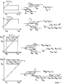
- FIG. 3 is an illustration of a glitch bottleneck example.
- the glitch bottleneck ratio is used to identify glitch bottleneck pins. Determining glitch power efficiently comprises identifying glitch bottleneck pins. Before identifying glitch bottleneck pins, the bottleneck ratio is calculated for every pin.
- the bottleneck ratio on a leaf output pin for example pin ( 302 ) at the output of gate U 4 ( 304 ), is set as 1.
- the circuit is then backward traversed to calculate the bottleneck ratios for other pins in the fan-in cone, which as shown in FIG. 3 includes pins associated with gate U 2 ( 306 ) and U 1 ( 308 ).
- a circuit in an analysis engine a circuit is abstracted into a directed graph.
- the logic gate input/output pins are represented as vertices in the graph.
- the timing arc from input to output pin in the same logic gate or the connection from one logic gate output to the other logic gate input are represented as edges in the graph.
- a starting vertex and ending vertex may be defined.
- Typical starting vertices include: primary input ports and/or sequential logic gate output pins (e.g. flip-flop Q pins).
- Typical ending vertices include: primary output ports and/or sequential logic gate inputs (e.g. flip-flop D pins).
- backward traversal is traversing this directed graph from ending vertices to input vertices.
- Ratio BN(i) is defined as the bottleneck ratio on pin i.
- the bottleneck ratio of an input pin a is represented as:
- BN ⁇ ( a ) P ⁇ ( ⁇ F ⁇ a ) * BN ⁇ ( o )
- F is the output function of a cell
- P( ⁇ F/ ⁇ a) is the probability of the Boolean difference
- BN(o) is the bottleneck ratio of output pin.
- the value of the Boolean difference reflects the fact of change of the function F with respect to one of its variable a; the Boolean difference is equal to 1 if such change occurs, and is equal to 0 otherwise.
- the bottleneck ratio of an output pin is 1 plus its total bottleneck ratio on sink pins.
- the critical bottleneck pins may be found by multiplying the bottleneck ratio for a given pin with its generated glitch power or propagated glitch power, as described in greater detail below.
- the most critical bottleneck pin may be found by sorting Ptotal.
- Using a glitch bottleneck is disclosed, for example, for each instance output pin. This results in the total glitch toggles caused by the pin in its fanout cone.
- implementation/P&R optimization may focus on high glitch bottleneck pins to reduce the design glitch power effectively.
- FIG. 4 is an illustration of a glitch power bottleneck calculation using a statistical glitch power analysis.
- the pin glitch power bottleneck ratio of a pin may be expressed as the total glitch toggle rate at the pin propagated to its fanout.
- an approximate glitch power bottleneck is the bottleneck ratio multiplied by the pin glitch power.
- the bottleneck ratio of the whole design may be calculated using a one forward depth-first traverse.
- w i is a glitch toggle propagation rate calculated during statistical glitch power analysis
- o 1 is the output pin ( 404 ) of gate ( 408 )
- w 1 is the glitch toggle propagation ratefor arc i 1 to o 1 ( 406 ) calculated during statistical glitch power analysis.
- BN( i 2) BN( o 2) ⁇ w 2
- BN( i 3) BN( o 3) ⁇ w 3
- BN( i 4) BN( o 4) ⁇ w 4
- ⁇ y ⁇ x i term is the Boolean difference of Boolean function y related to it's i-th variable x i .
- P ⁇ ( ⁇ y ⁇ x i ) term represents me probability of the Boolean difference to have value 1.
- the ⁇ j! i (1 ⁇ Tog_Rate(x j )) term multiplies all of (1 ⁇ Tog_Rate(x j )) together where x j the j-th variable of y and j is any variable in the variable list but i.
- FIG. 5 is a flow chart illustrating an embodiment of a process for dynamic power analysis. In one embodiment, the process of FIG. 5 is carried out by the system of FIG. 1 .
- a logic gate glitch pattern is generated. That is, the input patterns that may cause a glitch at each logic gate output in the design are characterized.
- a class definition for such an input pattern may be:
- the generated logic gate glitch pattern may be used, for example, in step ( 512 ) as part of determining generated glitch power.
- a signal/switching activity report is accessed.
- the signal/switching activity report is imported from a VCD file.
- Other data formats and access can be used in other embodiments.
- switching activity and signal probability are calculated based on information from the signal/switching activity report, for example a VCD file.
- the tool propagates switching activity and signal probability to fill-in missing information.
- the total toggle count per time duration is its switching activity, wherein the time duration for each pin when its logic is one is its signal probability.
- the signal probability P(x) is the average fraction of clock cycles in which the steady state value of the node x is a logic high:
- step ( 510 ) dynamic power is analyzed.
- the dynamic power is a function of the sum of switching power and internal power.
- the signal probability and switching activity may be annotated from the VCD file of step ( 504 ).
- the toggle activity may be extracted, for example by using a command.
- the AP the computing engine may perform signal probability and switching activity propagation using the function in equation (1).
- the internal power of one gate i is determined based on
- PW table (j) is an internal power table associated with timing arc from input j to the output of gate i; and SWA ij is part of the gate output switching activity assigned to each input based on equation (1).
- each arc signal probability also may be applied during this internal power estimation.
- a statistical generated glitch power is determined.
- a statistical engine calculates generated glitch toggles at all instance outputs.
- the generated glitches at an instance output are caused by functional toggles at its inputs.
- the output generated glitch values depend on:
- a pattern probability is referred to herein as the probability that an input glitch generating pattern ⁇ k occurs.
- P patt ′( ⁇ k ) is the probability that two inputs toggling together, wherein considering two toggling inputs has traditionally been accurate enough.
- P patt ′ ( ⁇ k ) D ⁇ ( a ) / 2 f c ⁇ l ⁇ k ⁇ D ⁇ ( b ) / 2 f c ⁇ l ⁇ k
- D(x) is the switching activity of x, as described above.
- a generated glitch may occur under the condition that the interval time ⁇ between successive transitions at different inputs is larger than cell delay ⁇ .
- R g ⁇ e ⁇ n ( i ) f c ⁇ l ⁇ k ⁇ ⁇ k ⁇ P g ⁇ e ⁇ n ( ⁇ k ) ⁇ P p ⁇ a ⁇ t ⁇ t ( ⁇ k ) ⁇ wherein f clk is clock frequency.
- FIG. 6 is an illustration of a uniform distribution model to determine a generated glitch rate. Assuming a uniform distribution function in that the toggle may evenly occur with arrival window
- f ⁇ ( t ) 1 ( ⁇ max - ⁇ min ) ⁇ ⁇ U ⁇ ( t - ⁇ min ) - U ⁇ ( t - ⁇ max ) ⁇
- ⁇ max is the latest arrival time
- ⁇ min is the earliest arrival time (without OCV or On Chip Variation)
- U is the step function/uniform distribution function.
- the area “A 1 ” represents the glitch pattern when pin A is leading edge (R)
- the area “A 2 ” represents the glitch pattern when pin B is leading edge (R).
- FIG. 7 is an illustration of a uniform distribution model surface integration analysis. As shown in FIG. 7 in various cases, for area A 1 :
- R gen (i) two main techniques are disclosed: gate sizing down in order to increase ⁇ a , and adjusting the input arrival time to reduce the generation probability P gen .
- the statistical generated glitch power may be calculated as described above.
- a statistical propagated glitch power is determined.
- the propagated glitches at a logic gate output is caused by glitch toggles at its input pins.
- One simplifying model assumes the inputs of gate have no correlation with each other; and/or there is sufficient time interval between the input transitions to calculate a simpler output propagating glitch rate as:
- x i the i-th input of the gate
- y the output
- n the total number of inputs.
- side input is a related input of a given gate, so that the inputs of the gate are deterministic and/or statistically correlated.
- a more accurate algorithm may be developed to calculate propagated glitch that considers side input toggle impact, such as when multiple side inputs are switching simultaneously, which reduces the glitch propagation rate.
- P ⁇ ( ⁇ y ⁇ x i ) is the signal probability of the Boolean difference.
- R(x i ) is the glitch rate of the gate's i th input x i
- R ( x i ) R gen ( x i )+ R prop ( x i ).
- Beta(y, x j ) approximates SID using side-inputs correlated relationships, and is useful to determine signal activity on all side-input nodes of a Boolean function.
- the weighting coefficients ⁇ 1 , ⁇ 2 , and ⁇ 3 are set to 1.0.
- the SID number is applied to all arcs (logic arc from input x i to output y) of the Boolean function as a simplified approximation to calculate the R prop (y).
- the process stops here if no further weighting coefficients fine-tuning is required.
- the stopping criteria may be determined by comparing the calculated R prop (y) with golden number derived from, for example, VCD input or calculated using the exact method of multiple-variable Boolean difference probability from a number of digital gates.
- a self-tuned machine learning mechanisms may be applied to derive the weighting coefficients ⁇ 1, ⁇ 3, ⁇ 3 ⁇ .
- gradient descent, K-means clustering or simplified convolutionalneural networks (CNN) methods are applied to find a set of best fitted weighting coefficients for different gate groups, with improved R prop accuracy.
- Some of the results are served as a testing set.
- the training, the repeating of deriving and testing, is executed on the fly and stops once the stopping criteria can be satisfied.
- the weighting coefficients found are applied on the rest of the design. They may be stored in the database to be reused, and as a starting point to train other designs.
- Beta(y, x j ) of a single input gate is 1 since there are no side-inputs to disturb.
- the Beta(y, x j ) of a two input gate (2-input NOR, NAND, XOR) can be reduced to (1 ⁇ R(x j )) where x j is the side-input.
- the Beta(y, x j ) of a three input gate (3-input NOR, NAND, XOR) may be reduced to (1 ⁇ 0.5*(R(x 2 )+R(x 3 ))) where x 2 , x 3 are side-inputs and x 1 is the input calculated on.
- the sum approaches 0 when the side-input pin's toggle rate approaches 1, which indicates that no glitches may propagate through the gate.
- Beta(y, x i ) represents the correlation of the non-toggled side-inputs 1 ⁇ (1 ⁇ R(x i )) to its neighbors (1 ⁇ R(x k )), one at a time. The sum is normalized.
- Beta(y, x i ) represents the correlation of non-toggled side-inputs 1 ⁇ (1 ⁇ R(x j )) to their neighbors (1 ⁇ R(x k )), all at once. The sum is normalized.
- Beta(y, x i ) above compensates the double counting of the multiplication of non-toggled side-inputs. The sum is normalized. This prevents the R prop from being too pessimistic at the global level but may have a tendency of skewing the result towards optimistic on gates with many inputs.
- step ( 518 ) a glitch bottleneck ratio is determined.
- the techniques described herein associated with FIG. 3 are used to determine the glitch bottleneck ratio.
- an incremental TC and TG calculation is used. If TC anno is a total toggle count and TG anno is a total glitch edges in AP, which are calculated after a file like a VCD file is imported. TC anno and TG anno are updated in an incremental timing update based on a TG stat change from the statistical engine:
- FIG. 8 is a flow chart illustrating an embodiment of a process for glitch power optimization.
- the process of FIG. 8 is carried out by the system of FIG. 1 .
- Optimization is one application of the dynamic power analysis of FIG. 5 .
- Reducing the glitch power consumption commences with a determination of bottleneck gates through an MCMM (Multi-Corner Multi-Mode) based bottleneck glitch power analysis query. For each selected gate, performing optimization techniques including gate sizing and repeater removal to reduce glitch power while checking timing and other design QoR (Quality of Results) metrics.
- MCMM Multi-Corner Multi-Mode
- a timer performs MCMM timing update and calculates glitch power of the design.
- an optimizer queries generated glitch power bottleneck driver pins through a timer's glitch power analysis function.
- the optimizer selects gates with an upper bound for power consumption greater than a predetermined threshold value. The optimizer selects optimizable candidate gates to put into a gate list and sorts the gate list by timing criticality.
- step ( 808 ) for each selected candidate gate the optimizer uses hazard filtering and arrival timing balancing techniques to reduce generated glitch power through the gate.
- hazard filtering gate propagation delays are adjusted to filter out glitches through the gate.
- a gate is replaced by a logically equivalent but different sized cell so that a delay of the gate is changed.
- the optimizer uses gate upsizing and gate downsizing techniques to balance arrival time through the gate.
- step ( 810 ) after optimization for generated glitch power reduction, a timer performs bottleneck-based propagated glitch power analysis.
- step ( 812 ) the optimizer selects repeater type gates from bottleneck-based gates with propagated glitch power, and sorts them with timing criticality. These candidate gates are put into a gate list for propagated glitch power reduction.
- step ( 814 ) propagated glitch power is reduced in part by applying buffer removal and/or inverter pair merge/removal.
- step ( 816 ) in the event glitch power reduction meets a target or the process hits the maximum/threshold number of loops, control is ended; otherwise, control is transferred back to step ( 804 ) for another loop.
- FIG. 9 is an illustration of optimization techniques to reduce generated glitch power.
- a candidate gate is U 3 ( 902 ).
- a hazard filtering technique is used to increase the delay of gate U 3 ( 902 ) to such an extent so that the glitch is eliminated and hence generated glitch power on gate U 3 ( 902 ) is eliminated.
- Upsizing gate U 1 ( 904 ) with slower path delay or downsizing gate U 2 ( 906 ) with faster path delay may reduce glitching transition so that the generated glitch power is reduced.
- gate U 3 ( 902 ) is a buffer type, then it may be removed to eliminate its propagated glitch power if there is no QoR degradation. If gate U 3 ( 902 ) is an inverter type and gate U 4 ( 908 ) is also an inverter type, then gate U 3 ( 902 ) and gate U 4 ( 908 ) may be merged or removed for generated power reduction.
- FIG. 10A is a flow chart illustrating an embodiment of a process for glitch power analysis. In one embodiment, the process of FIG. 10A is carried out by the system of FIG. 1 .
- a switching activity report of simulated switching activities of a semiconductor circuit is accessed.
- a switching activity report may be and/or includes a VCD file.
- accurate glitch toggle information is determined based at least in part on the switching activity report.
- Accurate glitch toggle information may be based at least in part on an annotation engine analysis of the switching activity report.
- boundary pin toggling information is used to determine statistical glitch toggle information.
- Boundary pins as described herein are the input pins and output pins of registers.
- statistical glitch toggle information is based at least in part on a statistical engine estimate such as TG stat described above.
- parameters associated with side-input disturbance are determined using machine learning.
- side-input disturbance is accounted for using a first-order approximation, for example as described above.
- side-input disturbance is accounted for using a correlation of non-toggled side inputs, for example as described above.
- a plurality of glitch counts corresponding to a plurality of gate output pins from the switching activity report are extracted and a plurality of accurate glitch powers based on the plurality of glitch counts determined. In one embodiment, a plurality of glitch powers corresponding to the plurality of pins is determined.
- updated statistical glitch toggle information is determined incrementally based on the adjustment, applying the calibration ratio to the updated statistical glitch toggle information.
- step ( 1004 ) a plurality of glitch bottleneck ratios corresponding to a plurality of pins in the semiconductor circuit is determined, as described in more detail below in FIG. 10B
- a plurality of total glitch powers associated with the plurality of pins is determined, wherein each total glitch power of the plurality of total glitch powers being determined based on a glitch bottleneck ratio and a glitch power of a corresponding pin.
- the total glitch power is based at least in part on a function of the glitch bottleneck ratio multiplied by the glitch power of the corresponding pin.
- the glitch power of the corresponding pin is based at least in part on one of the following: a generated glitch power for the corresponding pin and a propagated power for the corresponding pin.
- step ( 1008 ) one or more critical bottleneck pins among the plurality of pins is identified based on the plurality of total glitch powers.
- step ( 1010 ) one or more gates associated with the one or more critical bottleneck pins is adjusted to reduce corresponding one or more total glitch powers of the one or more gates.
- the adjusting of the one or more gates includes one or more of: balancing the signal toggling time at gate inputs; changing gate delay; making a gate delay larger; applying glitch filtering; and/or changing clock latency of a clock tree.
- An optimizer such as AprisaTM by Avatar Integrated Systems can be used to perform step ( 1008 ) and/or step ( 1010 ).
- FIG. 10B is a flow chart illustrating an embodiment of a process for determining glitch bottleneck ratios corresponding to pins.
- the process of FIG. 10B is part of step ( 1004 ) in FIG. 10A and carried out by the system of FIG. 1 .
- step ( 1050 ) an initial bottleneck ratio is set on a leaf output pin, for example pin ( 302 ) at the output of gate U 4 ( 304 ) in FIG. 3 .
- step ( 1052 ) the semiconductor circuit is backward traversed to determine a plurality of glitch bottleneck ratios of pins in a fan-in cone of the leaf output pin, for example in FIG. 3 the fan-in cone of pin ( 302 ) includes pins associated with gate U 2 ( 306 ) and U 1 ( 308 ).
- a dual glitch power analysis engine has been disclosed.
- a dual glitch power analysis engine calculates accurate glitch power value and incrementally updates design glitch power during, for example, an implementation/P&R flow.
- One of the two engines is an annotation engine which extracts information from, for example, a VCD file and annotates accurate glitch toggle information from the dynamic simulation that produced the file.
- the other of the two engines is a statistical engine which uses boundary pin toggling information.
- One benefit of this practical dual glitch power analysis engine is improved analysis and optimization on reducing dynamic power during circuit design and implementation. For the target design this may improve battery life, reduce heat and/or thermal noise, improve power efficiency, reduce power requirements, and reduce weight/size of a product associated with the target design.
Abstract
Description
-
- dynamic gate-level simulation, for example VCS or NCSIM, to generate zero and non-zero delay SAIF files;
- using a single non-zero delay VCD file is sufficient to extract a glitch toggle rate per instance/gate; and/or
- a power analysis tool reads the VCD file, SAIF file, or other signal/switching report to perform dynamic, functional, and/or glitch power analysis.
After applying this calibration ratio, the initial glitch power from the two engines is similar.
where F is the output function of a cell, P(∂F/∂a) is the probability of the Boolean difference, and BN(o) is the bottleneck ratio of output pin. The value of the Boolean difference reflects the fact of change of the function F with respect to one of its variable a; the Boolean difference is equal to 1 if such change occurs, and is equal to 0 otherwise.
BN(U4_o)=1
BN(U5_o)=1
and the bottleneck ratio of the other output pins for U1_o, U2_o, and U3_o, the output pin of gates U1 (308), U2 (306), and U3 (312) respectively, are:
BN(U1_o)=1+BN(U2_a)+BN(U3_a)
BN(U2_o)=1+BN(U4_a)
BN(U3_o)=1+BN(U5_a)
Ptotal(o)=BN(o)*Pglitch(o)
where Pglitch(o) is the glitch power on pin o and BN(o) is the bottleneck ratio on pin o. The most critical bottleneck pin may be found by sorting Ptotal.
BN(i1)=BN(o1)×w 1
where o1 is the output pin (404) of gate (408), and w1 is the glitch toggle propagation ratefor arc i1 to o1 (406) calculated during statistical glitch power analysis. Similarly:
BN(i2)=BN(o2)×w 2
BN(i3)=BN(o3)×w 3
BN(i4)=BN(o4)×w 4
BN(o3)=1+BN(i1)+BN(i2).
Generally,
Here the
term is the Boolean difference of Boolean function y related to it's i-th variable xi. The
term represents me probability of the Boolean difference to have
| class powGlitchPattern |
| { |
| dbLibPin* | _oPin; | // output pin with glitch |
| dbLibPin* | _leadPin; | // Input pin with leading edge |
| dbLibPin* | _tailPin; | // Input pin with tailing edge |
| bool | _leadEdgeFall; | // Leading edge polarity |
| bool | _tailEdgeFall; | // Tailing edge polarity |
| // 0 |
||
| DdNode* | _biasCondition; | // Bias condition BoolTree |
| powGlitchPattern* | _next; | // Next glitch input pattern |
| }; |
| with generation being executed as: |
| foreach inCell arc (input: inP1) that trigger R at outP { |
| collect inP pointer into array1; |
| also record inP toggle (R/F) into toggleArr1; |
| } |
| foreach inCell arc (input: inP2) that trigger F at outP { |
| collect inP2 pointer into array2; |
| also record inP2 toggle (R/F) into toggleArr2; |
| } |
| foreach inP1 in arrag1 { |
| foreach inP2 in arragZ { |
| if (inP1 == inP2) continue; |
| // following code need decide which input can be the leading edge |
| if (toggleArr1 [inP1] == R && toggleArr2 [inP1] = R) { |
| // assuming inP1 lead. in temporal domain. |
| // the input logic combination for |
| // inP1/inP is 00, 10, 11 |
| Eval BoolTree of output pin: |
| val1 = outP_Bool (inP1 == 0. inP2 == 0) ; |
| Eval BoolTree of output pin: |
| val2 = outP_Bool (inP1 == 1. inP2 == 0) ; |
| Eval BoolTree of output pin: |
| val3 = outP_Bool (inP1 == 1. inP2 == 1) ; |
| if (val1 == val3 && val1 != val2) then |
| inP1 lead, inP2 tail is valid pattern; |
| // assuming inP1 tail, inP2 lead. then |
| // the input logic is: 00, 01. 11 |
| Eval BoolTree of output pin: |
| val4 2 outP_Bool (inP1 == 0. inP2 == 1) ; |
| if (val1 == val3 && val1 != val4) then |
| inP1 tail, inP2 lead is valid pattern; |
| } |
| else if (toggleArr1 [inP1] == R && toggleArr2 [inP1] == F) { |
| // similar |
| } |
| else if (toggleArr1 [inP1] == F & toggleArr2 [inP1] == R) { |
| // similar |
| }else { // (toggleArr1 [inP1] == F && toggleArr2 [inP1] == F) |
| // similar |
| } |
| } |
| } |
TC=TCfunc +TG anno
Wherein TCfunc is a functional toggle count at each instance. During a power optimization flow, this number may be constant.
wherein a(y) is switching activity on output pin y and are second order Boolean differences that consider both input xi and xj switching simultaneously. The Boolean expression for their calculations are:
P(x) represents the probability of the second order Boolean differences to have
P sw i=½C load V 2 SWA
wherein Cload is the gate output loading capacitance; V is the gate supply voltage; and SW A is the gate output switching activity.
wherein PWtable(j) is an internal power table associated with timing arc from input j to the output of gate i; and SWAij is part of the gate output switching activity assigned to each input based on equation (1). In the event the same input has multiple conditional arcs, each arc signal probability also may be applied during this internal power estimation.
-
- TCfunc at its input pins, the leading and tailing pins in the glitch pattern;
- cell delay from leading input pin to the output pin;
- the arrival times at its input pins, the leading and tailing pins in the glitch pattern; and/or
- the Boolean function of the logic gate.
P patt(ωk)=P patt′(ωk)·P(ωi,bias)
where D(x) is the switching activity of x, as described above.
P gen(ωk)=∫∫A
wherein α and β are the arrival times of the respective signals/inputs in ωk, f is the distribution function representing the number of transitions as a function of arrival time, and Ak is the area that satisfies the condition that the interval time ζ between successive transitions at different inputs is larger than cell delay τ.
wherein fclk is clock frequency.
wherein αmax is the latest arrival time and αmin is the earliest arrival time (without OCV or On Chip Variation), and U is the step function/uniform distribution function. As shown in
-
- if βmax≤αmin+τa, then Pgen=0;
- if βmin≤αmin+τa, then
-
- if βmax≤αmax+τa, then and
-
- if δmin≤αmax+τa, then
-
- if βmax≤αmin+τa, then Pgen=0;
- if βmax≤αmax+τa, then
-
- if βmin≤αmin+τa, then and
-
- if βmin≤αmax+τa, then
Wherein xi is the i-th input of the gate, y is the output and n is the total number of inputs.
may not consider side input toggling impacts and tends to overestimate propagated glitch.
wherein
is the Boolean difference of output y with respect to ith input xi, and
is the signal probability of the Boolean difference. R(xi) is the glitch rate of the gate's ith input xi,
R(x i)=R gen(x i)+R prop(x i).
in the equation of Beta(y, xi) above represents the correlation of the non-toggled side-
in the equation of Beta(y, xi) above represents the correlation of non-toggled side-
wherein TGstat new is the new statistical glitch count, and TGstat base is the statistical glitch count before the incremental optimization change:
TCanno new=(TCanno orig −TG anno orig)+TG anno new
Claims (20)
Priority Applications (1)
| Application Number | Priority Date | Filing Date | Title |
|---|---|---|---|
| US16/915,099 US11509303B2 (en) | 2020-06-03 | 2020-06-29 | Glitch power analysis and optimization engine |
Applications Claiming Priority (2)
| Application Number | Priority Date | Filing Date | Title |
|---|---|---|---|
| US202063034189P | 2020-06-03 | 2020-06-03 | |
| US16/915,099 US11509303B2 (en) | 2020-06-03 | 2020-06-29 | Glitch power analysis and optimization engine |
Publications (2)
| Publication Number | Publication Date |
|---|---|
| US20210384901A1 US20210384901A1 (en) | 2021-12-09 |
| US11509303B2 true US11509303B2 (en) | 2022-11-22 |
Family
ID=75040932
Family Applications (1)
| Application Number | Title | Priority Date | Filing Date |
|---|---|---|---|
| US16/915,099 Active 2041-05-19 US11509303B2 (en) | 2020-06-03 | 2020-06-29 | Glitch power analysis and optimization engine |
Country Status (2)
| Country | Link |
|---|---|
| US (1) | US11509303B2 (en) |
| CN (1) | CN112560373A (en) |
Families Citing this family (2)
| Publication number | Priority date | Publication date | Assignee | Title |
|---|---|---|---|---|
| US11748534B1 (en) * | 2022-01-11 | 2023-09-05 | Cadence Design Systems, Inc. | System and method for glitch power estimation |
| CN114580345B (en) * | 2022-04-29 | 2022-07-05 | 深圳鸿芯微纳技术有限公司 | Circuit simulation method and device, computer equipment and computer readable storage medium |
Citations (5)
| Publication number | Priority date | Publication date | Assignee | Title |
|---|---|---|---|---|
| US6016066A (en) * | 1998-03-19 | 2000-01-18 | Intel Corporation | Method and apparatus for glitch protection for input buffers in a source-synchronous environment |
| KR20010098552A (en) * | 2000-04-13 | 2001-11-08 | 가부시키가이샤 어드밴티스트 | Glitch detection for semiconductor test system |
| US7372304B2 (en) * | 2005-10-04 | 2008-05-13 | Stmicroelectronics, Inc. | System and method for glitch detection in a secure microcontroller |
| US20080281574A1 (en) * | 2007-05-07 | 2008-11-13 | Ryan Bazinet | System and method for glitch analysis in circuits |
| US11361137B2 (en) * | 2020-06-03 | 2022-06-14 | Siemens Industry Software Inc. | Integrated simulator and analysis and optimization engine |
-
2020
- 2020-06-29 US US16/915,099 patent/US11509303B2/en active Active
- 2020-08-25 CN CN202010863535.7A patent/CN112560373A/en active Pending
Patent Citations (5)
| Publication number | Priority date | Publication date | Assignee | Title |
|---|---|---|---|---|
| US6016066A (en) * | 1998-03-19 | 2000-01-18 | Intel Corporation | Method and apparatus for glitch protection for input buffers in a source-synchronous environment |
| KR20010098552A (en) * | 2000-04-13 | 2001-11-08 | 가부시키가이샤 어드밴티스트 | Glitch detection for semiconductor test system |
| US7372304B2 (en) * | 2005-10-04 | 2008-05-13 | Stmicroelectronics, Inc. | System and method for glitch detection in a secure microcontroller |
| US20080281574A1 (en) * | 2007-05-07 | 2008-11-13 | Ryan Bazinet | System and method for glitch analysis in circuits |
| US11361137B2 (en) * | 2020-06-03 | 2022-06-14 | Siemens Industry Software Inc. | Integrated simulator and analysis and optimization engine |
Non-Patent Citations (3)
| Title |
|---|
| Hashimoto et al., "A Practical Gate Resizing Technique Considering Glitch Reduction for Low Power Design", Proceedings of the 36th annual Design Automation Conference, Jun. 1999. |
| Lim et al., "Statistical Estimation of Delay-Dependent Switching Activities in Embedded CMOS Combinational Circuits", IEEE Trans. on Very Large Scale Integration (VLSI) Systems, vol. 5, No. 3, Sep. 1997. |
| Sayed et al., "A New Statistical Approach for Glitch Estimation in Combinational Circuits", IEEE Internal Symposium on Circuits and Systems, May 2007. |
Also Published As
| Publication number | Publication date |
|---|---|
| CN112560373A (en) | 2021-03-26 |
| US20210384901A1 (en) | 2021-12-09 |
Similar Documents
| Publication | Publication Date | Title |
|---|---|---|
| US7890915B2 (en) | Statistical delay and noise calculation considering cell and interconnect variations | |
| US7383522B2 (en) | Crosstalk-aware timing analysis | |
| US7685549B2 (en) | Method of constrained aggressor set selection for crosstalk induced noise | |
| US9881123B1 (en) | Method and system for timing analysis with adaptive timing window optimization for determining signal integrity impact | |
| Agarwal et al. | Statistical clock skew analysis considering intradie-process variations | |
| US10467365B1 (en) | Systems and methods for calculating common clock path pessimism for hierarchical timing analysis in an electronic design | |
| US20070283305A1 (en) | System and Method for Providing an Improved Sliding Window Scheme for Clock Mesh Analysis | |
| US11509303B2 (en) | Glitch power analysis and optimization engine | |
| US10423742B2 (en) | Method to perform full accuracy hierarchical block level timing analysis with parameterized chip level contexts | |
| US11361137B2 (en) | Integrated simulator and analysis and optimization engine | |
| US8549448B2 (en) | Delay optimization during circuit design at layout level | |
| US10296700B1 (en) | Multimode circuit place and route optimization | |
| US10534883B1 (en) | Local path-based analysis for circuit place and route optimization | |
| US8495544B2 (en) | Statistical delay and noise calculation considering cell and interconnect variations | |
| US9342642B1 (en) | Statistical optimization in place-and-route | |
| US7222039B2 (en) | Estimation of average-case activity for digital state machines | |
| Chang et al. | Type-matching clock tree for zero skew clock gating | |
| Sapatnekar | Static timing analysis | |
| US10534878B1 (en) | Circuit place and route optimization based on path-based timing analysis | |
| US7191417B1 (en) | Method and apparatus for optimization of digital integrated circuits using detection of bottlenecks | |
| US10133842B1 (en) | Methods, systems, and articles of manufacture for multi-mode, multi-corner physical optimization of electronic designs | |
| US6760894B1 (en) | Method and mechanism for performing improved timing analysis on virtual component blocks | |
| US20200401669A1 (en) | Clock gate latency modeling based on analytical frameworks | |
| US7941679B2 (en) | Method for computing power savings and determining the preferred clock gating circuit of an integrated circuit design | |
| Held | Gate sizing for large cell-based designs |
Legal Events
| Date | Code | Title | Description |
|---|---|---|---|
| FEPP | Fee payment procedure |
Free format text: ENTITY STATUS SET TO UNDISCOUNTED (ORIGINAL EVENT CODE: BIG.); ENTITY STATUS OF PATENT OWNER: LARGE ENTITY |
|
| AS | Assignment |
Owner name: MENTOR GRAPHICS CORPORATION, OREGON Free format text: SECURITY INTEREST;ASSIGNOR:AVATAR INTEGRATED SYSTEMS, INC.;REEL/FRAME:053288/0081 Effective date: 20200722 |
|
| AS | Assignment |
Owner name: AVATAR INTEGRATED SYSTEMS, INC., CALIFORNIA Free format text: RELEASE BY SECURED PARTY;ASSIGNOR:MENTOR GRAPHICS CORPORATION;REEL/FRAME:053558/0632 Effective date: 20200821 |
|
| AS | Assignment |
Owner name: AVATAR INTEGRATED SYSTEMS, INC., CALIFORNIA Free format text: ASSIGNMENT OF ASSIGNORS INTEREST;ASSIGNORS:BAI, GENG;TZENG, PING-SAN;WANG, CHAO-YUNG;AND OTHERS;SIGNING DATES FROM 20200727 TO 20200728;REEL/FRAME:053579/0770 |
|
| AS | Assignment |
Owner name: SIEMENS INDUSTRY SOFTWARE INC., TEXAS Free format text: MERGER;ASSIGNOR:AVATAR INTEGRATED SYSTEMS, INC.;REEL/FRAME:055388/0136 Effective date: 20201130 |
|
| AS | Assignment |
Owner name: SIEMENS INDUSTRY SOFTWARE INC., TEXAS Free format text: MERGER AND CHANGE OF NAME;ASSIGNORS:AVATAR INTEGRATED SYSTEMS, INC.;SIEMENS INDUSTRY SOFTWARE INC.;REEL/FRAME:055666/0360 Effective date: 20201130 |
|
| STPP | Information on status: patent application and granting procedure in general |
Free format text: NOTICE OF ALLOWANCE MAILED -- APPLICATION RECEIVED IN OFFICE OF PUBLICATIONS |
|
| STCF | Information on status: patent grant |
Free format text: PATENTED CASE |