US11509133B2 - Transient voltage suppression device - Google Patents
Transient voltage suppression device Download PDFInfo
- Publication number
- US11509133B2 US11509133B2 US17/132,389 US202017132389A US11509133B2 US 11509133 B2 US11509133 B2 US 11509133B2 US 202017132389 A US202017132389 A US 202017132389A US 11509133 B2 US11509133 B2 US 11509133B2
- Authority
- US
- United States
- Prior art keywords
- coupled
- diode
- transient voltage
- conductivity type
- common bus
- Prior art date
- Legal status (The legal status is an assumption and is not a legal conclusion. Google has not performed a legal analysis and makes no representation as to the accuracy of the status listed.)
- Active, expires
Links
Images




Classifications
-
- H—ELECTRICITY
- H02—GENERATION; CONVERSION OR DISTRIBUTION OF ELECTRIC POWER
- H02H—EMERGENCY PROTECTIVE CIRCUIT ARRANGEMENTS
- H02H9/00—Emergency protective circuit arrangements for limiting excess current or voltage without disconnection
- H02H9/04—Emergency protective circuit arrangements for limiting excess current or voltage without disconnection responsive to excess voltage
-
- H—ELECTRICITY
- H02—GENERATION; CONVERSION OR DISTRIBUTION OF ELECTRIC POWER
- H02H—EMERGENCY PROTECTIVE CIRCUIT ARRANGEMENTS
- H02H9/00—Emergency protective circuit arrangements for limiting excess current or voltage without disconnection
- H02H9/005—Emergency protective circuit arrangements for limiting excess current or voltage without disconnection avoiding undesired transient conditions
-
- H—ELECTRICITY
- H02—GENERATION; CONVERSION OR DISTRIBUTION OF ELECTRIC POWER
- H02H—EMERGENCY PROTECTIVE CIRCUIT ARRANGEMENTS
- H02H9/00—Emergency protective circuit arrangements for limiting excess current or voltage without disconnection
- H02H9/04—Emergency protective circuit arrangements for limiting excess current or voltage without disconnection responsive to excess voltage
- H02H9/045—Emergency protective circuit arrangements for limiting excess current or voltage without disconnection responsive to excess voltage adapted to a particular application and not provided for elsewhere
- H02H9/046—Emergency protective circuit arrangements for limiting excess current or voltage without disconnection responsive to excess voltage adapted to a particular application and not provided for elsewhere responsive to excess voltage appearing at terminals of integrated circuits
-
- H—ELECTRICITY
- H10—SEMICONDUCTOR DEVICES; ELECTRIC SOLID-STATE DEVICES NOT OTHERWISE PROVIDED FOR
- H10D—INORGANIC ELECTRIC SEMICONDUCTOR DEVICES
- H10D89/00—Aspects of integrated devices not covered by groups H10D84/00 - H10D88/00
- H10D89/60—Integrated devices comprising arrangements for electrical or thermal protection, e.g. protection circuits against electrostatic discharge [ESD]
- H10D89/601—Integrated devices comprising arrangements for electrical or thermal protection, e.g. protection circuits against electrostatic discharge [ESD] for devices having insulated gate electrodes, e.g. for IGFETs or IGBTs
- H10D89/611—Integrated devices comprising arrangements for electrical or thermal protection, e.g. protection circuits against electrostatic discharge [ESD] for devices having insulated gate electrodes, e.g. for IGFETs or IGBTs using diodes as protective elements
Definitions
- the present invention relates to a suppression device, particularly to a transient voltage suppression device.
- Electrostatic Discharge (ESD) damage has become the main reliability issue for CMOS IC products fabricated in the nanoscale CMOS processes.
- ESD protection device is generally designed to bypass the ESD energy, so that the IC chips can be prevented from ESD damages.
- FIG. 1 illustrates a circuit diagram of a conventional low-capacitance transient voltage suppressor.
- the transient voltage suppressor 1 includes a power clamp device 10 and a plurality of first diodes 12 and a plurality of second diodes 14 .
- one or more diodes are usually arranged between input output terminals I/O 1 and I/O 2 and a power terminal PWR and between the input output terminals I/O 1 and I/O 2 and a ground terminal GND in conventional technical field so the equivalent capacitances on the current dissipation paths may be reduced through parasitic capacitances on the diodes connected in series.
- the diodes additionally arranged on each channel may cause a circuit area required by the transient voltage suppressor to increase significantly and thereby dramatically increase circuit costs.
- the present invention provides a transient voltage suppression device, so as to solve the afore-mentioned problems of the prior art.
- the present invention provides a transient voltage suppression device, which flexibly adjusts and reduces the parasitic capacitance of an electrostatic discharge (ESD) path and adjusts the holding voltage of the ESD path under the premise that the circuit area may be saved.
- ESD electrostatic discharge
- a transient voltage suppression device includes at least one diode string, a power clamp device, at least one first bypass diode, and at least two second bypass diodes.
- the diode string is coupled between a power terminal and a common bus and coupled to an input output (I/O) port.
- the power clamp device is coupled between the power terminal and the common bus.
- the first bypass diode is coupled between the common bus and a ground terminal.
- the second bypass diodes is coupled in series, coupled between the common bus and the ground terminal, and coupled to the first bypass diode in reverse parallel.
- the anode of the first bypass diode is coupled to the common bus.
- the cathode of the first bypass diode is coupled to the ground terminal.
- the cathode of the second bypass diodes is coupled to the common bus.
- the anode of the second bypass diodes is coupled to the ground terminal.
- the diode string includes a first diode and a second diode.
- the anode of the first diode is coupled to the I/O port.
- the cathode of the first diode is coupled to the power terminal.
- the anode of the second diode is coupled to the common bus.
- the cathode of the second diode is coupled to the I/O port.
- the at least one diode string includes a plurality of diode strings.
- the at least one first bypass diode includes a plurality of first bypass diodes coupled in series.
- a node between two of the plurality of first bypass diodes is coupled to a node between the second bypass diodes.
- the cathode of the first bypass diode is coupled to the common bus.
- the anode of the first bypass diode is coupled to the ground terminal.
- the anode of the second bypass diodes is coupled to the common bus.
- the cathode of the second bypass diodes is coupled to the ground terminal.
- a transient voltage suppression device includes at least one diode string, a power clamp device, and at least one bi-directional electrostatic discharge (ESD) device.
- the diode string coupled between a power terminal and a common bus and coupled to an input output (I/O) port is coupled between a power terminal and a common bus and coupled to an input output (I/O) port.
- the power clamp device is coupled between the power terminal and the common bus.
- the bi-directional electrostatic discharge device is coupled between the common bus and a ground terminal.
- the diode string includes a first diode and a second diode.
- the anode of the first diode is coupled to the I/O port.
- the cathode of the first diode is coupled to the power terminal.
- the anode of the second diode is coupled to the common bus.
- the cathode of the second diode is coupled to the I/O port.
- the bi-directional ESD device is a metal-oxide-semiconductor field effect transistor (MOSFET), a bipolar junction transistor (BJT), or a silicon-controlled rectifier (SCR).
- MOSFET metal-oxide-semiconductor field effect transistor
- BJT bipolar junction transistor
- SCR silicon-controlled rectifier
- the at least one diode string includes a plurality of diode strings.
- the at least one bi-directional ESD device comprises a plurality of bi-directional ESD devices coupled in series.
- the diode string and the power clamp device are formed in a semiconductor substrate.
- the semiconductor substrate has a first conductivity type.
- the bi-directional ESD device includes a first doped well, a second doped well, a first heavily-doped area, and a second heavily-doped area.
- the doped well, having a second conductivity type opposite to the first conductivity type is formed in the semiconductor substrate.
- the second doped well, having the second conductivity type is formed in the semiconductor substrate.
- the first heavily-doped area, having the second conductivity type is formed in the first doped well and coupled to the common bus.
- the second heavily-doped area, having the first conductivity type is formed in the first doped well and coupled to the common bus.
- the third heavily-doped area, having the second conductivity type is formed in the second doped well and coupled to the ground terminal.
- the fourth heavily-doped area, having the first conductivity type is formed in the second doped well and coupled to the ground terminal.
- the first conductivity type is an N type and the second conductivity type is a P type.
- the first conductivity type is a P type and the second conductivity type is an N type.
- the diode string and the power clamp device are formed in a semiconductor substrate.
- the semiconductor substrate has a first conductivity type.
- the bi-directional ESD device includes a doped well, a first heavily-doped area, and a second heavily-doped area.
- the doped well having a second conductivity type opposite to the first conductivity type, is formed in the semiconductor substrate.
- the doped well is floating.
- the first heavily-doped area, having the first conductivity type is formed in the doped well and coupled to the ground terminal.
- the second heavily-doped area, having the first conductivity type is formed in the doped well and coupled to the common bus.
- the bi-directional ESD device further includes an insulation layer and an electrode layer sequentially formed on the doped well.
- the electrode layer is floating.
- the transient voltage suppression device connects either the at least one first bypass diode and the at least two second bypass diodes or the at least one bi-directional electrostatic discharge (ESD) device to adjust and reduce the parasitic capacitance of an electrostatic discharge (ESD) path and adjust the holding voltage of the ESD path under the premise that the circuit area may be saved.
- ESD electrostatic discharge
- FIG. 1 is a schematic diagram illustrating a transient voltage suppressor in the conventional technology
- FIG. 2 is a schematic diagram illustrating a transient voltage suppression device according to a first embodiment of the present invention
- FIG. 3 is a schematic diagram illustrating a transient voltage suppression device according to a second embodiment of the present invention.
- FIG. 4 is a schematic diagram illustrating a transient voltage suppression device according to a third embodiment of the present invention.
- FIG. 5 is a schematic diagram illustrating a transient voltage suppression device according to a fourth embodiment of the present invention.
- FIG. 6 is a schematic diagram illustrating a transient voltage suppression device according to a fifth embodiment of the present invention.
- FIG. 7 is a schematic diagram illustrating a transient voltage suppression device according to a sixth embodiment of the present invention.
- FIG. 8 is a schematic diagram illustrating a transient voltage suppression device according to a seventh embodiment of the present invention.
- FIG. 9 is a cross-sectional view of a transient voltage suppression device according to a first implementation corresponding to the sixth embodiment of the present invention.
- FIG. 10 is a cross-sectional view of a transient voltage suppression device according to a second implementation corresponding to the sixth embodiment of the present invention.
- FIG. 11 is a cross-sectional view of a transient voltage suppression device according to a third implementation corresponding to the sixth embodiment of the present invention.
- FIG. 12 is a cross-sectional view of a transient voltage suppression device according to a fourth implementation corresponding to the sixth embodiment of the present invention.
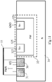
- FIG. 13 is a cross-sectional view of a transient voltage suppression device according to a fifth implementation corresponding to the sixth embodiment of the present invention.
- FIG. 14 is a cross-sectional view of a transient voltage suppression device according to a sixth implementation corresponding to the sixth embodiment of the present invention.
- FIG. 15 is a diagram illustrating normalized capacitance versus voltage curves of the first embodiment, the third embodiment, and the sixth embodiment of the present invention.
- conditional sentences or words such as “can”, “could”, “might”, or “may”, usually attempt to express that the embodiment in the present invention has, but it can also be interpreted as a feature, element, or step that may not be needed. In other embodiments, these features, elements, or steps may not be required.
- a transient voltage suppression device For the purpose of flexibly adjusting and reducing the parasitic capacitance of an electrostatic discharge (ESD) path and adjusts the holding voltage of the ESD path under the premise that the circuit area may be saved, a transient voltage suppression device is provided.
- ESD electrostatic discharge
- FIG. 2 is a schematic diagram illustrating a transient voltage suppression device according to a first embodiment of the present invention.
- the transient voltage suppression device 2 includes at least one diode string 20 , a power clamp device 21 , at least one first bypass diode 22 , and at least two second bypass diodes 23 .
- the power clamp device 21 may be a Zener diode, a bipolar junction transistor, a silicon-controlled rectifier, or a metal-oxide-semiconductor field-effect transistor.
- the diode string 20 is coupled between a power terminal PWR and a common bus 24 and coupled to an input output (I/O) port.
- the power clamp device 21 is coupled between the power terminal PWR and the common bus 24 .
- the first bypass diode 22 is coupled between the common bus 24 and a ground terminal GND.
- the second bypass diodes 23 are coupled in series, coupled between the common bus 24 and the ground terminal GND, and coupled to the first bypass diode 22 in reverse parallel.
- the anode of the first bypass diode 22 is coupled to the common bus 24 .
- the cathode of the first bypass diode 22 is coupled to the ground terminal GND.
- the cathode of the second bypass diode 23 most near to the common bus 24 is coupled to the common bus 24 .
- the anode of the second bypass diode 23 most near to the ground terminal GND is coupled to the ground terminal GND.
- the diode string 20 may include a first diode 201 and a second diode 202 .
- the anode of the first diode 201 is coupled to the I/O port.
- the cathode of the first diode 201 is coupled to the power terminal PWR.
- the anode of the second diode 202 is coupled to the common bus 24 .
- the cathode of the second diode 202 is coupled to the I/O port.
- the operation of the transient voltage suppression device 2 is introduced as follows.
- an electrostatic discharge voltage higher than the ground voltage of the ground terminal GND appears at the I/O port an electrostatic discharge current flows from the I/O port to the ground terminal GND through the first diode 201 , the power clamp device 21 , the common bus 24 , and the first bypass diode 22 .
- an electrostatic discharge voltage lower than the ground voltage of the ground terminal GND appears at the I/O port an electrostatic discharge current flows from the ground terminal GND to the I/O port through the second bypass diodes 23 , the common bus 24 , and the second diode 202 .
- one current dissipation path may be generated by arranging the first diode 201 between the I/O port and the power terminal PWR in cooperation with the first bypass diode 22 .
- another current dissipation path may be generated by arranging the second diode 202 between the I/O port and the common bus 24 in cooperation with the second bypass diodes 23 .
- the equivalent capacitances on the current dissipation paths may all be effectively reduced and adjusted through the first bypass diode 22 coupled to the first diode 201 in series or through the second bypass diodes 23 coupled to the second diode 202 in series to improve the effectiveness of the ESD protection.
- the holding voltage of the current dissipation paths may be flexibly adjusted.
- the equivalent capacitances on the current dissipation paths may all be effectively reduced without correspondingly arranging additional diodes, such that a layout area required by the transient voltage suppression device 2 may be effectively saved.
- FIG. 3 is a schematic diagram illustrating a transient voltage suppression device according to a second embodiment of the present invention.
- the second embodiment is different from the first embodiment in the number of the diode strings 20 .
- the second embodiment exemplifies a plurality of diode strings 20 each coupled to one I/O port.
- the anode of the first bypass diode 22 and the cathode of the second bypass diode 23 are coupled to the common bus 24 .
- FIG. 4 is a schematic diagram illustrating a transient voltage suppression device according to a third embodiment of the present invention.
- the third embodiment of the transient voltage suppression device 2 is introduced as follows.
- the third embodiment is different from the first embodiment in the first bypass diode 22 and the second bypass diodes 23 .
- the third embodiment exemplifies a plurality of first bypass diodes 22 coupled in series.
- a node between two of the plurality of first bypass diodes 22 may be coupled to a node between the second bypass diodes 23 .
- the first nodes are respectively coupled to the second nodes.
- FIG. 5 is a schematic diagram illustrating a transient voltage suppression device according to a fourth embodiment of the present invention.
- the transient voltage suppression device 2 includes at least one diode string 20 , a power clamp device 21 , at least one first bypass diode 22 , and at least two second bypass diodes 23 .
- the diode string 20 is coupled between a power terminal PWR and a common bus 24 and coupled to an input output (I/O) port.
- the power clamp device 21 is coupled between the power terminal PWR and the common bus 24 .
- the first bypass diode 22 is coupled between the common bus 24 and a ground terminal GND.
- the second bypass diodes 23 are coupled in series, coupled between the common bus 24 and the ground terminal GND, and coupled to the first bypass diode 22 in reverse parallel.
- the cathode of the first bypass diode 22 is coupled to the common bus 24 .
- the anode of the first bypass diode 22 is coupled to the ground terminal GND.
- the anode of the second bypass diode 23 most near to the common bus 24 is coupled to the common bus 24 .
- the cathode of the second bypass diode 23 most near to the ground terminal GND is coupled to the ground terminal GND.
- the diode string 20 may include a first diode 201 and a second diode 202 .
- the anode of the first diode 201 is coupled to the I/O port.
- the cathode of the first diode 201 is coupled to the power terminal PWR.
- the anode of the second diode 202 is coupled to the common bus 24 .
- the cathode of the second diode 202 is coupled to the I/O port.
- the operation of the transient voltage suppression device 2 is introduced as follows.
- an electrostatic discharge voltage higher than the ground voltage of the ground terminal GND appears at the I/O port an electrostatic discharge current flows from the I/O port to the ground terminal GND through the first diode 201 , the power clamp device 21 , the common bus 24 , and the second bypass diodes 23 .
- an electrostatic discharge voltage lower than the ground voltage of the ground terminal GND appears at the I/O port an electrostatic discharge current flows from the ground terminal GND to the I/O port through the first bypass diodes 22 , the common bus 24 , and the second diode 202 .
- one current dissipation path may be generated by arranging the first diode 201 between the I/O port and the power terminal PWR in cooperation with the second bypass diodes 23 .
- another current dissipation path may be generated by arranging the second diode 202 between the I/O port and the common bus 24 in cooperation with the first bypass diode 22 .
- the equivalent capacitances on the current dissipation paths may all be effectively reduced and adjusted through the second bypass diodes 23 coupled to the first diode 201 in series or through the first bypass diode 22 coupled to the second diode 202 in series to improve the effectiveness of the ESD protection.
- the holding voltage of the current dissipation paths may be flexibly adjusted.
- the equivalent capacitances on the current dissipation paths may all be effectively reduced without correspondingly arranging additional diodes, such that a layout area required by the transient voltage suppression device 2 may be effectively saved.
- FIG. 6 is a schematic diagram illustrating a transient voltage suppression device according to a fifth embodiment of the present invention.
- the fifth embodiment is different from the fourth embodiment in the number of the diode strings 20 .
- the fifth embodiment exemplifies a plurality of diode strings 20 each coupled to one I/O port.
- the cathode of the first bypass diode 22 and the anode of the second bypass diode 23 are coupled to the common bus 24 .
- FIG. 7 is a schematic diagram illustrating a transient voltage suppression device according to a sixth embodiment of the present invention. Referring to FIG.
- the transient voltage suppression device 3 includes at least one diode string 30 , a power clamp device 31 , and at least one bi-directional electrostatic discharge (ESD) device 32 .
- the diode string 30 is coupled between a power terminal PWR and a common bus 33 and coupled to an input output (I/O) port.
- the power clamp device 31 is coupled between the power terminal PWR and the common bus 33 .
- the bi-directional electrostatic discharge device 32 such as a metal-oxide-semiconductor field effect transistor (MOSFET), a bipolar junction transistor (BJT), or a silicon-controlled rectifier (SCR), is coupled between the common bus 33 and a ground terminal GND.
- MOSFET metal-oxide-semiconductor field effect transistor
- BJT bipolar junction transistor
- SCR silicon-controlled rectifier
- a plurality of bi-directional ESD devices 32 coupled in series can be used.
- the bi-directional electrostatic discharge device 32 replaces the first bypass diode and the second bypass diode to reduce the more layout area.
- the bi-directional electrostatic discharge device 32 has a current gain and a lower holding voltage.
- the bi-directional electrostatic discharge device 32 has better ESD performance than a diode.
- the ESD robustness level of the ESD component is lower since the ESD component is easily burnt out.
- the bi-directional electrostatic discharge device 32 having a higher breakdown voltage cooperates with ESD clamping components between bus lines to sustain the operating voltage of an internal circuit
- the ESD clamping components can be designed to have lower breakdown voltage.
- the entire ESD protection circuit has a higher ESD robustness level.
- the diode string 30 may include a first diode 301 and a second diode 302 .
- the anode of the first diode 301 is coupled to the I/O port.
- the cathode of the first diode 301 is coupled to the power terminal PWR.
- the anode of the second diode 302 is coupled to the common bus 33 .
- the cathode of the second diode 302 is coupled to the I/O port.
- the operation of the transient voltage suppression device 3 is introduced as follows.
- an electrostatic discharge voltage higher than the ground voltage of the ground terminal GND appears at the I/O port an electrostatic discharge current flows from the I/O port to the ground terminal GND through the first diode 301 , the power clamp device 31 , the common bus 33 , and the bi-directional electrostatic discharge device 32 .
- an electrostatic discharge voltage lower than the ground voltage of the ground terminal GND appears at the I/O port an electrostatic discharge current flows from the ground terminal GND to the I/O port through the bi-directional electrostatic discharge device 32 , the common bus 33 , and the second diode 302 .
- one current dissipation path may be generated by arranging the first diode 301 between the I/O port and the power terminal PWR in cooperation with the bi-directional electrostatic discharge device 32 .
- another current dissipation path may be generated by arranging the second diode 302 between the I/O port and the common bus 33 in cooperation with the bi-directional electrostatic discharge device 32 .
- the equivalent capacitances on the current dissipation paths may all be effectively reduced and adjusted through the bi-directional electrostatic discharge device 32 coupled to the first diode 301 in series or coupled to the second diode 302 in series to improve the effectiveness of the ESD protection.
- the bi-directional electrostatic discharge device 32 due to the bi-directional electrostatic discharge device 32 , the holding voltage of the current dissipation paths may be flexibly adjusted.
- the equivalent capacitances on the current dissipation paths may all be effectively reduced without correspondingly arranging additional diodes, such that a layout area required by the transient voltage suppression device 3 may be effectively saved.
- FIG. 8 is a schematic diagram illustrating a transient voltage suppression device according to a seventh embodiment of the present invention.
- the seventh embodiment is different from the sixth embodiment in the number of the diode strings 30 .
- the seventh embodiment exemplifies a plurality of diode strings 30 each coupled to one I/O port.
- the bi-directional electrostatic discharge device 32 is coupled to the common bus 33 .
- FIG. 9 is a cross-sectional view of a transient voltage suppression device according to a first implementation corresponding to the sixth embodiment of the present invention. Referring to FIG. 9 , the diode string 30 and the power clamp device 31 are formed in a semiconductor substrate 34 .
- the semiconductor substrate 34 has a first conductivity type.
- the bi-directional ESD device 32 is exemplified by a silicon-controlled rectifier.
- the bi-directional ESD device 32 may include a first doped well 320 , a first heavily-doped area 321 , a second heavily-doped area 322 , a third heavily-doped area 323 , a fourth heavily-doped area 324 , and a second doped well 320 ′.
- the first doped well 320 having a second conductivity type opposite to the first conductivity type, is formed in the semiconductor substrate 34 .
- the first conductivity type is an N type and the second conductivity type is a P type.
- the second doped well 320 ′, having the second conductivity type, is formed in the semiconductor substrate 34 .
- the first heavily-doped area 321 having the second conductivity type, is formed in the first doped well 320 and coupled to the common bus 33 .
- the second heavily-doped area 322 having the first conductivity type, is formed in the first doped well 320 and coupled to the common bus 33 .
- the third heavily-doped area 323 having the second conductivity type, is formed in the second doped well 320 ′ and coupled to the ground terminal GND.
- the fourth heavily-doped area 324 having the first conductivity type, is formed in the second doped well 320 ′ and coupled to the ground terminal GND.
- FIG. 10 is a cross-sectional view of a transient voltage suppression device according to a second implementation corresponding to the sixth embodiment of the present invention.
- the second implementation is different from the first implementation in the conductivity type.
- the first conductivity type is a P type and the second conductivity type is an N type.
- the other structures have been described previously in the first implementation so will not be reiterated.
- FIG. 11 is a cross-sectional view of a transient voltage suppression device according to a third implementation corresponding to the sixth embodiment of the present invention.
- the diode string 30 and the power clamp device 31 are formed in a semiconductor substrate 34 .
- the semiconductor substrate 34 has a first conductivity type.
- the bi-directional ESD device 32 is exemplified by a bipolar junction transistor.
- the bi-directional ESD device 32 may include a doped well 325 , a first heavily-doped area 326 , and a second heavily-doped area 327 .
- the doped well 325 having a second conductivity type opposite to the first conductivity type, is formed in the semiconductor substrate 34 .
- the doped well 325 is floating.
- the first conductivity type is an N type and the second conductivity type is a P type.
- the first heavily-doped area 326 having the first conductivity type, is formed in the doped well 325 and coupled to the ground terminal GND.
- the second heavily-doped area 327 having the first conductivity type, is formed in the doped well 325 and coupled to the common bus 33 .
- the third implementation lacks two heavily-doped areas and thus a smaller layout area.
- FIG. 12 is a cross-sectional view of a transient voltage suppression device according to a fourth implementation corresponding to the sixth embodiment of the present invention.
- the fourth implementation is different from the third implementation in the conductivity type.
- the first conductivity type is a P type and the second conductivity type is an N type.
- the other structures have been described previously in the third implementation so will not be reiterated.
- FIG. 13 is a cross-sectional view of a transient voltage suppression device according to a fifth implementation corresponding to the sixth embodiment of the present invention. As illustrated in FIG. 13 , compared with the third implementation, the fifth implementation further includes an insulation layer 328 and an electrode layer 329 sequentially formed on the doped well 325 . The electrode layer 329 is floating.
- the bi-directional ESD device 32 is exemplified by a metal-oxide-semiconductor field effect transistor.
- FIG. 14 is a cross-sectional view of a transient voltage suppression device according to a sixth implementation corresponding to the sixth embodiment of the present invention. As illustrated in FIG. 14 , compared with the fourth implementation, the sixth implementation further includes an insulation layer 328 and an electrode layer 329 sequentially formed on the doped well 325 . The electrode layer 329 is floating.
- the bi-directional ESD device 32 is exemplified by a metal-oxide-semiconductor field effect transistor.
- FIG. 15 is a diagram illustrating normalized capacitance versus voltage curves of the first embodiment, the third embodiment, and the sixth embodiment of the present invention. Referring to FIG. 15 , the capacitance on the current dissipation path of the first embodiment or the third embodiment is higher than that of the sixth embodiment.
- the equivalent capacitances on the current dissipation paths may be reduced accordingly.
- the capacitance values and the holding voltage of the transient voltage suppression device may be adjusted or reduced under premise that the circuit area is not increased to improve the effectiveness of the ESD protection.
Landscapes
- Engineering & Computer Science (AREA)
- Microelectronics & Electronic Packaging (AREA)
- Semiconductor Integrated Circuits (AREA)
Abstract
Description
Claims (8)
Priority Applications (3)
| Application Number | Priority Date | Filing Date | Title |
|---|---|---|---|
| US17/132,389 US11509133B2 (en) | 2020-12-23 | 2020-12-23 | Transient voltage suppression device |
| TW110113891A TWI763442B (en) | 2020-12-23 | 2021-04-19 | Transient voltage suppression device |
| CN202110496211.9A CN113345883B (en) | 2020-12-23 | 2021-05-07 | Transient voltage suppression device |
Applications Claiming Priority (1)
| Application Number | Priority Date | Filing Date | Title |
|---|---|---|---|
| US17/132,389 US11509133B2 (en) | 2020-12-23 | 2020-12-23 | Transient voltage suppression device |
Publications (2)
| Publication Number | Publication Date |
|---|---|
| US20220200272A1 US20220200272A1 (en) | 2022-06-23 |
| US11509133B2 true US11509133B2 (en) | 2022-11-22 |
Family
ID=77469821
Family Applications (1)
| Application Number | Title | Priority Date | Filing Date |
|---|---|---|---|
| US17/132,389 Active 2041-01-07 US11509133B2 (en) | 2020-12-23 | 2020-12-23 | Transient voltage suppression device |
Country Status (3)
| Country | Link |
|---|---|
| US (1) | US11509133B2 (en) |
| CN (1) | CN113345883B (en) |
| TW (1) | TWI763442B (en) |
Families Citing this family (2)
| Publication number | Priority date | Publication date | Assignee | Title |
|---|---|---|---|---|
| US12136621B2 (en) * | 2022-01-11 | 2024-11-05 | Amazing Microelectronic Corp. | Bidirectional electrostatic discharge (ESD) protection device |
| CN118825933B (en) * | 2024-08-06 | 2025-06-03 | 无锡英迪芯微电子科技股份有限公司 | An electrostatic protection circuit |
Citations (10)
| Publication number | Priority date | Publication date | Assignee | Title |
|---|---|---|---|---|
| US6501630B1 (en) | 1999-12-17 | 2002-12-31 | Koninklijke Philips Electronics N.V. | Bi-directional ESD diode structure |
| US20050270712A1 (en) | 2004-06-02 | 2005-12-08 | Shao-Chang Huang | Multi-domain ESD protection circuit structure |
| TW201025618A (en) | 2008-12-23 | 2010-07-01 | Amazing Microelectronic Corp | Bi-directional transient voltage suppression device and forming method thereof |
| US20130314824A1 (en) * | 2012-05-22 | 2013-11-28 | Synopsys, Inc. | Preventing electrostatic discharge (esd) failures across voltage domains |
| US20170302072A1 (en) * | 2016-04-14 | 2017-10-19 | Ubiq Semiconductor Corp. | Multi-channel transient voltage suppressor |
| US10468513B1 (en) * | 2018-08-30 | 2019-11-05 | Amazing Microelectronic Corp. | Bidirectional silicon-controlled rectifier |
| US20200043911A1 (en) * | 2018-07-31 | 2020-02-06 | Richwave Technology Corp. | Anti-parallel diode device |
| TW202015180A (en) | 2018-09-12 | 2020-04-16 | 晶焱科技股份有限公司 | Ultra-low capacitance transient voltage suppressor |
| TW202017143A (en) | 2018-10-26 | 2020-05-01 | 大陸商萬民半導體(澳門)有限公司 | Low capacitance transient voltage suppressor |
| US20210384870A1 (en) * | 2020-06-05 | 2021-12-09 | Analog Devices, Inc. | Apparatus and methods for amplifier input-overvoltage protection with low leakage current |
Family Cites Families (8)
| Publication number | Priority date | Publication date | Assignee | Title |
|---|---|---|---|---|
| KR100470994B1 (en) * | 1997-10-06 | 2005-07-07 | 삼성전자주식회사 | Semiconductor of esd(electrostatic discharge)protection apparatus |
| TW575989B (en) * | 2002-09-25 | 2004-02-11 | Mediatek Inc | NPN Darlington ESD protection circuit |
| TW200905859A (en) * | 2007-07-31 | 2009-02-01 | Amazing Microelectroing Corp | Asymmetric type bi-directional silicon control rectifier |
| US9466978B2 (en) * | 2013-08-30 | 2016-10-11 | Taiwan Semiconductor Manufacturing Company, Ltd. | Electrostatic discharge protection for level-shifter circuit |
| US10573635B2 (en) * | 2018-07-23 | 2020-02-25 | Amazing Microelectronics Corp. | Transient voltage suppression device with improved electrostatic discharge (ESD) robustness |
| US10504886B1 (en) * | 2018-09-05 | 2019-12-10 | Hong Kong Applied Science and Technology Research Institute Company, Limited | Low-capacitance electro-static-discharge (ESD) protection structure with two floating wells |
| CN109545782A (en) * | 2018-11-29 | 2019-03-29 | 上海华力集成电路制造有限公司 | A kind of electrostatic discharge protective circuit and semiconductor structure |
| US11387648B2 (en) * | 2019-01-10 | 2022-07-12 | Analog Devices International Unlimited Company | Electrical overstress protection with low leakage current for high voltage tolerant high speed interfaces |
-
2020
- 2020-12-23 US US17/132,389 patent/US11509133B2/en active Active
-
2021
- 2021-04-19 TW TW110113891A patent/TWI763442B/en active
- 2021-05-07 CN CN202110496211.9A patent/CN113345883B/en active Active
Patent Citations (11)
| Publication number | Priority date | Publication date | Assignee | Title |
|---|---|---|---|---|
| US6501630B1 (en) | 1999-12-17 | 2002-12-31 | Koninklijke Philips Electronics N.V. | Bi-directional ESD diode structure |
| US20050270712A1 (en) | 2004-06-02 | 2005-12-08 | Shao-Chang Huang | Multi-domain ESD protection circuit structure |
| TW201025618A (en) | 2008-12-23 | 2010-07-01 | Amazing Microelectronic Corp | Bi-directional transient voltage suppression device and forming method thereof |
| US20130314824A1 (en) * | 2012-05-22 | 2013-11-28 | Synopsys, Inc. | Preventing electrostatic discharge (esd) failures across voltage domains |
| US20170302072A1 (en) * | 2016-04-14 | 2017-10-19 | Ubiq Semiconductor Corp. | Multi-channel transient voltage suppressor |
| US10270242B2 (en) | 2016-04-14 | 2019-04-23 | Upi Semiconductor Corp. | Multi-channel transient voltage suppressor |
| US20200043911A1 (en) * | 2018-07-31 | 2020-02-06 | Richwave Technology Corp. | Anti-parallel diode device |
| US10468513B1 (en) * | 2018-08-30 | 2019-11-05 | Amazing Microelectronic Corp. | Bidirectional silicon-controlled rectifier |
| TW202015180A (en) | 2018-09-12 | 2020-04-16 | 晶焱科技股份有限公司 | Ultra-low capacitance transient voltage suppressor |
| TW202017143A (en) | 2018-10-26 | 2020-05-01 | 大陸商萬民半導體(澳門)有限公司 | Low capacitance transient voltage suppressor |
| US20210384870A1 (en) * | 2020-06-05 | 2021-12-09 | Analog Devices, Inc. | Apparatus and methods for amplifier input-overvoltage protection with low leakage current |
Also Published As
| Publication number | Publication date |
|---|---|
| CN113345883B (en) | 2024-03-05 |
| CN113345883A (en) | 2021-09-03 |
| TWI763442B (en) | 2022-05-01 |
| TW202226513A (en) | 2022-07-01 |
| US20220200272A1 (en) | 2022-06-23 |
Similar Documents
| Publication | Publication Date | Title |
|---|---|---|
| TWI713189B (en) | Low capacitance transient voltage suppressor | |
| US11482519B2 (en) | Transient voltage suppressor and method for manufacturing the same | |
| US10497697B2 (en) | Low capacitance transient voltage suppressor | |
| US8455315B2 (en) | Symmetric blocking transient voltage suppressor (TVS) using bipolar transistor base snatch | |
| US7102199B2 (en) | Low voltage transient voltage suppressor and method of making | |
| KR20160007425A (en) | Transient voltage protection circuits and devices | |
| US10270242B2 (en) | Multi-channel transient voltage suppressor | |
| US8859361B1 (en) | Symmetric blocking transient voltage suppressor (TVS) using bipolar NPN and PNP transistor base snatch | |
| US20220200272A1 (en) | Transient voltage suppression device | |
| US12107084B2 (en) | Multi-channel transient voltage suppression device | |
| TWI683414B (en) | Improved transient voltage suppression device | |
| US20030141545A1 (en) | Semiconductor device | |
| US6456474B2 (en) | Semiconductor integrated circuit | |
| US20230215864A1 (en) | Bidirectional electrostatic discharge (esd) protection device | |
| US20220052035A1 (en) | Vertical electrostatic discharge protection device | |
| CN114388495A (en) | Integrated clamping diode structure and forming method | |
| US11271099B2 (en) | Vertical bipolar transistor device | |
| CN107946299B (en) | A load switch and electronic equipment | |
| US20240234408A1 (en) | Electrostatic discharge (esd) protection device | |
| CN118523274B (en) | Composite electrostatic and surge protection circuit | |
| US12027846B2 (en) | Electrostatic protection structure and electrostatic protection circuit | |
| US20250357754A1 (en) | Electrostatic discharge protection device | |
| CN116207094B (en) | Electrostatic and surge protection circuit applied to high-speed transmission interface chip | |
| CN112670281A (en) | Bidirectional low-voltage electrostatic surge full-chip protection integrated circuit | |
| CN121531786A (en) | Transient Voltage Suppressor and its Fabrication Method |
Legal Events
| Date | Code | Title | Description |
|---|---|---|---|
| FEPP | Fee payment procedure |
Free format text: ENTITY STATUS SET TO UNDISCOUNTED (ORIGINAL EVENT CODE: BIG.); ENTITY STATUS OF PATENT OWNER: SMALL ENTITY |
|
| AS | Assignment |
Owner name: AMAZING MICROELECTRONIC CORP., TAIWAN Free format text: ASSIGNMENT OF ASSIGNORS INTEREST;ASSIGNORS:YEH, CHIH-TING;HUANG, SUNG-CHIH;CHUANG, CHE-HAO;REEL/FRAME:054807/0964 Effective date: 20201222 |
|
| FEPP | Fee payment procedure |
Free format text: ENTITY STATUS SET TO SMALL (ORIGINAL EVENT CODE: SMAL); ENTITY STATUS OF PATENT OWNER: SMALL ENTITY |
|
| STPP | Information on status: patent application and granting procedure in general |
Free format text: RESPONSE TO NON-FINAL OFFICE ACTION ENTERED AND FORWARDED TO EXAMINER |
|
| STPP | Information on status: patent application and granting procedure in general |
Free format text: FINAL REJECTION MAILED |
|
| STPP | Information on status: patent application and granting procedure in general |
Free format text: RESPONSE AFTER FINAL ACTION FORWARDED TO EXAMINER |
|
| STPP | Information on status: patent application and granting procedure in general |
Free format text: NOTICE OF ALLOWANCE MAILED -- APPLICATION RECEIVED IN OFFICE OF PUBLICATIONS |
|
| STCF | Information on status: patent grant |
Free format text: PATENTED CASE |
|
| MAFP | Maintenance fee payment |
Free format text: PAYMENT OF MAINTENANCE FEE, 4TH YR, SMALL ENTITY (ORIGINAL EVENT CODE: M2551); ENTITY STATUS OF PATENT OWNER: SMALL ENTITY Year of fee payment: 4 |