US11508516B2 - Wireless charging module and electronic device thereof - Google Patents
Wireless charging module and electronic device thereof Download PDFInfo
- Publication number
- US11508516B2 US11508516B2 US16/829,912 US202016829912A US11508516B2 US 11508516 B2 US11508516 B2 US 11508516B2 US 202016829912 A US202016829912 A US 202016829912A US 11508516 B2 US11508516 B2 US 11508516B2
- Authority
- US
- United States
- Prior art keywords
- wireless charging
- charging module
- leads
- coil
- metal melting
- Prior art date
- Legal status (The legal status is an assumption and is not a legal conclusion. Google has not performed a legal analysis and makes no representation as to the accuracy of the status listed.)
- Active, expires
Links
Images


Classifications
-
- H—ELECTRICITY
- H01—ELECTRIC ELEMENTS
- H01F—MAGNETS; INDUCTANCES; TRANSFORMERS; SELECTION OF MATERIALS FOR THEIR MAGNETIC PROPERTIES
- H01F27/00—Details of transformers or inductances, in general
- H01F27/28—Coils; Windings; Conductive connections
- H01F27/29—Terminals; Tapping arrangements for signal inductances
-
- H—ELECTRICITY
- H01—ELECTRIC ELEMENTS
- H01F—MAGNETS; INDUCTANCES; TRANSFORMERS; SELECTION OF MATERIALS FOR THEIR MAGNETIC PROPERTIES
- H01F38/00—Adaptations of transformers or inductances for specific applications or functions
- H01F38/14—Inductive couplings
-
- H—ELECTRICITY
- H01—ELECTRIC ELEMENTS
- H01F—MAGNETS; INDUCTANCES; TRANSFORMERS; SELECTION OF MATERIALS FOR THEIR MAGNETIC PROPERTIES
- H01F27/00—Details of transformers or inductances, in general
- H01F27/28—Coils; Windings; Conductive connections
-
- H—ELECTRICITY
- H01—ELECTRIC ELEMENTS
- H01F—MAGNETS; INDUCTANCES; TRANSFORMERS; SELECTION OF MATERIALS FOR THEIR MAGNETIC PROPERTIES
- H01F27/00—Details of transformers or inductances, in general
- H01F27/28—Coils; Windings; Conductive connections
- H01F27/2823—Wires
- H01F27/2828—Construction of conductive connections, of leads
-
- H—ELECTRICITY
- H01—ELECTRIC ELEMENTS
- H01F—MAGNETS; INDUCTANCES; TRANSFORMERS; SELECTION OF MATERIALS FOR THEIR MAGNETIC PROPERTIES
- H01F27/00—Details of transformers or inductances, in general
- H01F27/34—Special means for preventing or reducing unwanted electric or magnetic effects, e.g. no-load losses, reactive currents, harmonics, oscillations, leakage fields
- H01F27/36—Electric or magnetic shields or screens
- H01F27/366—Electric or magnetic shields or screens made of ferromagnetic material
-
- H—ELECTRICITY
- H02—GENERATION; CONVERSION OR DISTRIBUTION OF ELECTRIC POWER
- H02J—CIRCUIT ARRANGEMENTS OR SYSTEMS FOR SUPPLYING OR DISTRIBUTING ELECTRIC POWER; SYSTEMS FOR STORING ELECTRIC ENERGY
- H02J50/00—Circuit arrangements or systems for wireless supply or distribution of electric power
-
- H—ELECTRICITY
- H02—GENERATION; CONVERSION OR DISTRIBUTION OF ELECTRIC POWER
- H02J—CIRCUIT ARRANGEMENTS OR SYSTEMS FOR SUPPLYING OR DISTRIBUTING ELECTRIC POWER; SYSTEMS FOR STORING ELECTRIC ENERGY
- H02J50/00—Circuit arrangements or systems for wireless supply or distribution of electric power
- H02J50/10—Circuit arrangements or systems for wireless supply or distribution of electric power using inductive coupling
-
- H—ELECTRICITY
- H02—GENERATION; CONVERSION OR DISTRIBUTION OF ELECTRIC POWER
- H02J—CIRCUIT ARRANGEMENTS OR SYSTEMS FOR SUPPLYING OR DISTRIBUTING ELECTRIC POWER; SYSTEMS FOR STORING ELECTRIC ENERGY
- H02J50/00—Circuit arrangements or systems for wireless supply or distribution of electric power
- H02J50/70—Circuit arrangements or systems for wireless supply or distribution of electric power involving the reduction of electric, magnetic or electromagnetic leakage fields
-
- H—ELECTRICITY
- H02—GENERATION; CONVERSION OR DISTRIBUTION OF ELECTRIC POWER
- H02J—CIRCUIT ARRANGEMENTS OR SYSTEMS FOR SUPPLYING OR DISTRIBUTING ELECTRIC POWER; SYSTEMS FOR STORING ELECTRIC ENERGY
- H02J7/00—Circuit arrangements for charging or depolarising batteries or for supplying loads from batteries
- H02J7/02—Circuit arrangements for charging or depolarising batteries or for supplying loads from batteries for charging batteries from AC mains by converters
-
- H02J7/70—
Definitions
- the present disclosure relates to the technical field of wireless charging, and more particularly to a wireless charging module and electronic device thereof for preventing tin liquid from flowing to a wireless charging coil.
- the wireless charging technology is a type of wireless power transmission technology.
- a power supply device charger
- a powered device that uses the received energy to charge the battery and simultaneously to operate the powered device.
- Wireless charging technology has the advantages of being safe, reliable, and convenient, and it could charge multiple electronic products at the same time without charging power cords. Also, different electronic products can be charged with the same wireless charging device.
- the use of coils has become more and more popular. The process of pre-tinning the coil conductor is necessary for testing the performance of the coil and combining the coil and other connectors.
- the ferrite and the coil when assembling the wireless charging module, the ferrite and the coil would be firstly assembled, and then the ferrite is welded to the base. During the welding process, the leads of the coil are firstly tinned, and the leads are then combined to the base.
- the liquid tin which is formed by melting the tin, on leads is pretty much flowable, and when the liquid tin flows to be in touched with the coil, the product is then flawed.
- the current method mainly focuses on testing of products, followed by eliminating products failed to pass the testing. Unfortunately, no proper solutions have been introduced so far for improving the rate of failure. Therefore, it is desirous to develop a solution to solve the problem that the liquid tin flows to the coil when the coil is welded to the base.
- the embodiment of the present disclosure provides a wireless charging module that solves the problem that the wireless charging module is flawed because the liquid tin from the leads flows to the wireless charging coil when the coil is welded to the base.
- the present disclosure provides a wireless charging module comprising a base, at least one magnetic shielding sheet, and a coil.
- the base comprises at least two metal melting regions. Each of the metal melting regions comprises an opening, and a blocking region is disposed at the opening.
- the magnetic shielding sheet is disposed on the base. The magnetic shielding sheet partially exposes the two metal melting regions and the opening.
- the coil is disposed on the magnetic shielding sheet.
- the coil comprises two leads. The two leads are respectively disposed on the two metal melting regions and are located in the blocking regions and the openings.
- the wires of coils could be disposed on the two metal melting regions.
- the two leads of the wire are close to the opening.
- the leads and the blocking regions are kept by a distance.
- the blocking region can be plated with a metal layer (such as nickel).
- the plated metal material of the metal melting region is different from the plated metal material of the blocking region.
- FIG. 1 is a schematic diagram of an electronic device of the present disclosure
- FIG. 2 is a perspective view of the wireless charging module of the present disclosure
- FIG. 3 is an exploded perspective view of FIG. 2 ;
- FIG. 4 is a partially enlarged view of FIG. 2 ;
- FIG. 5 is a schematic view of tinning of one embodiment of the present disclosure.
- FIG. 6 is another exploded perspective view of the wireless charging module of the present disclosure.
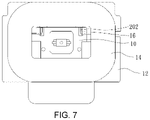
- FIG. 7 is a schematic diagram of the wireless charging module of another embodiment of the present disclosure.
- the terms “include”, “contain”, and any variation thereof are intended to cover a non-exclusive inclusion. Therefore, a process, method, object, or device that includes a series of elements not only include these elements, but also includes other elements not specified expressly, or may include inherent elements of the process, method, object, or device. If no more limitations are made, an element limited by “include a/an . . . ” does not exclude other same elements existing in the process, the method, the article, or the device which includes the element.
- FIG. 1 is a schematic diagram of an electronic device of the present disclosure.
- FIG. 2 is a perspective view of the wireless charging module of the present disclosure.
- FIG. 3 is an exploded perspective view of FIG. 2 .
- the electronic device 100 comprises a wireless charging module 1 and a power supply 2 .
- the wireless charging module 1 is electrically connected to the power supply 2 .
- the power supply 2 can be charged by the wireless charging module 1 .
- the wireless charging module 1 comprises a base 10 , at least one magnetic shielding sheet 12 , and a coil 14 .
- the base 10 comprises at least two metal melting regions 16 , each of the metal melting regions 16 has an opening 162 , and a blocking region 18 is disposed at the opening 162 .
- the magnetic shielding sheet 12 is disposed on the base 10 , and the magnetic shielding sheet 12 partially exposes the two metal melting regions 16 and the openings 162 , that is, the central portion of the magnetic shielding sheet 12 could be hollowed out.
- the magnetic shielding sheet 12 is designed according to the structure of the base 10 and the annular part of the coil 14 . That is, the coil 14 is disposed on the magnetic shielding sheet 12 , and the coil 14 is an annular part.
- the coil 14 also partially exposes the body of the base 10 and the two metal melting regions 16 and the openings 162 , which are located on the base 10 .
- the overall size of the magnetic shielding sheet 12 is larger than the size of the base 10 . Therefore, in addition to the exposed area, other portions of the magnetic shielding sheet 12 covers the base 10 , and the size of the coil 14 is smaller than the size of the magnetic shielding sheet 12 .
- the coil 14 can emit and receive energy for energy transferring, it mainly applies the principle of electromagnetic induction to transfer energy by energy coupling through the coil.
- Such coil 14 emits a high-frequency magnetic flux, and therefore, the magnetic shielding sheet 12 can be made of ferrite or soft magnetic metal material with specific characteristics for high-frequency purposes. In addition to shielding the high-frequency magnetic flux outputted from the coil 14 , it can also absorb and shield the magnetic flux from the magnet. Not only it can efficiently focus the magnetic field lines to improve power transmission efficiency, but also suppress the noise generation.
- the coil 14 is made by the process of winding the wire 20 .
- the winding process is an existing art and will not be described in detail herein.
- the two leads 202 of the wire 20 are respectively disposed on the two metal melting regions 16 and are disposed in the blocking regions 18 and the openings 162 .
- the lead 202 is closed to the opening 162 , and the lead 202 is kept from the blocking area 18 by a distance. Referring to FIG. 4 , which is a partial enlarged view of FIG.
- the lead 202 is separated from the blocking region 18 by a first distance D 1 on the extending direction of the lead 202
- the lead 202 is separated from the coil 14 by a second distance D 2 on the extending direction of the lead 202
- the first distance D 1 is shorter than the second distance D 2 .
- the first distance D 1 is 0.4 times to 1 time the width W 1 of the lead 202 , for example, 0.4 times, 0.5 times, 0.6 times, 0.7 times, 0.8 times, 0.9 times or 1 time.
- the second distance D 2 is 1.5 times to 2 times the width W 1 of the lead 202 , for example, 1.5 times, 1.6 times, 1.7 times, 1.8 times, 1.9 times or 2 times.
- the length L of the blocking region 18 is 0.2 times to 1 time the width W 2 of the blocking region 18 , for example, 0.2 times, 0.203 times, 0.3 times, 0.4 times, 0.5 times, 0.6 times, 0.7 times, 0.8 times, 0.9 times or 1.0 time.
- the thickness T of the blocking region 18 is 2 times to 3 times the width W 1 of the lead 202 , for example, 2 times, 2.1 times, 2.2 times, 2.3 times, 2.4 times, 2.5 times, 2.6 times, 2.7 times, 2.8 times, 2.9 times or 3 times.
- the first distance D 1 is 0.4 times to 0.5 times the width W 1 of the lead 202 , for example, 0.4 times, 0.45 times or 0.5 times.
- the second distance D 2 is 1.6 times to 2 times the width W 1 of the lead 202 , for example, 1.6 times, 1.7 times, 1.8 times, 1.9 times or 2 times.
- the width W 2 of the blocking region 18 is greater than the width W 3 of the opening 162 , the distance between the lead 202 of the two wires 20 and the inner ring edge of the coil 14 is 0.45 cm.
- the thickness W 2 of the blocking region 18 is 0.35, the distance between the lead 202 of the two wires 20 and the inner edge of the blocking region 18 is 0.1.
- the width W 4 of each metal melting region 16 is 4 to 5 times the width W 1 of each lead 202 .
- the width W 4 of each metal melting region 16 is 0.68 to 0.72
- the width W 1 of the lead 202 of each wire 20 is 0.25.
- the ratio of the width is designed according to various shapes of tinning for the lead 202 , such as a circle, a triangle, a T-shape or any geometric shapes.
- the height of the two metal melting regions 16 is 1.3 so the height of the blocking region 18 is greater than 1.3
- the gold plating has the advantages of good ductility, easy polishing, high-temperature resistance, long storage life and good resistance to discoloration; and of course, the metal layer can also be a layer of tin, because the liquid tin formed during the melting process of the wire tinning is also compatible with the tin plating layer. Therefore, the metal layer of the two metal melting regions 16 is not limited here by using a gold plating method or a tin plating method.
- the material of the metal melting region 16 is selected from the group consisting of gold and tin.
- the blocking region 18 can be plated with a metal layer, taking nickel as an example, the nickel plating layer has the advantages of high hardness, high wear resistance, high chemical stability, and etc.
- the metal material plated on the metal melting region 16 is different from the metal material plated on the blocking region 18 .
- FIG. 5 which is a schematic view of tinning of one embodiment of the present disclosure, after the two leads 202 are respectively tinned, they are disposed in the two metal melting regions 16 .
- the tin 22 on the two leads 202 turns to liquid phase during the melting process, and the liquid tin flows only within the two metal melting regions 16 .
- the two leads 202 of the embodiment only need to be bent once. Not only it simplifies the manufacturing process of the wireless charging module, but also further ensures the quality of the wireless charging module produced.
- FIG. 6 is another exploded perspective view of the wireless charging module of the present disclosure.
- the inner arrangement of the wireless charging module is identical or similar to those described above, so the same points are not described herein again and only the differences would be explained in the following.
- the magnetic shielding sheet 12 is configured with a high induction magnetic field and is configured for shielding the coil 14 , the characteristics and thickness of the magnetic shielding sheet 12 are designed in conjunction with the coil 14 . It is because, if the thickness of the magnetic shielding sheet 12 is too thin, the magnetic saturation problem may occur. The magnetic saturation could result in sudden decrease of the inductance of the coil 14 , which may cause an obstacle to the wireless charging.
- the two magnetic shielding sheets 12 and 12 ′ are disposed on the base 10 .
- the structures of the two magnetic shielding sheets 12 and 12 ′ may be identical, and the magnetic shielding sheets 12 and 12 ′ are correspondingly overlapped.
- the coil 14 is disposed on the second magnetic shielding sheet 12 ′, that is, the magnetic shielding sheet 12 ′ is disposed between the magnetic shielding sheet 12 and the coil 14 . It further improves the performance of the shielding coil 14 to emit high-frequency magnetic flux by increasing the thickness of the magnetic shielding sheet, which is achieved by using the two magnetic shielding sheets 12 and 12 ′.
- the two leads 202 of the wire 20 are disposed on the two metal melting regions 16 in a nearly parallel manner, although the disclosure is not limited thereto.
- the relative position between the two leads 202 of the wire 20 can also be in any other form, as shown in FIG. 7 , which is a schematic diagram of the wireless charging module of another embodiment of the present disclosure.
- the present disclosure provides a wireless charging module in which the width of the two metal melting regions 16 is wide enough to provide the tinned shape appearance required for the design of the lead 202 .
- the lead 202 is closed to the opening 162 , and the lead 202 is kept from the blocking area 18 by a distance.
- the blocking region 18 can be plated with a metal layer, in which the metal material of the metal layer plated on the metal melting region is different from that plated on the blocking region with different chemical properties.
- the metal layer plated on the blocking region 18 is incompatible with the tin on the lead 202 .
- the leads 202 of the two wires 20 are respectively tinted and then are placed in the two metal melting regions 16 .
- the tin on the two leads 202 turns to liquid phase during the melting process, and the liquid tin flows only within the two metal melting regions 16 .
- the liquid tin is blocked by the blocking area 18 , so the liquid tin does not flow to be in touched with the coil, thus the quality of the product could be ensured.
Landscapes
- Engineering & Computer Science (AREA)
- Power Engineering (AREA)
- Computer Networks & Wireless Communication (AREA)
- Physics & Mathematics (AREA)
- Electromagnetism (AREA)
- Charge And Discharge Circuits For Batteries Or The Like (AREA)
Abstract
Description
Claims (18)
Applications Claiming Priority (2)
| Application Number | Priority Date | Filing Date | Title |
|---|---|---|---|
| CN201911025753.7 | 2019-10-25 | ||
| CN201911025753.7A CN110610798B (en) | 2019-10-25 | 2019-10-25 | Wireless charging module |
Publications (2)
| Publication Number | Publication Date |
|---|---|
| US20210125774A1 US20210125774A1 (en) | 2021-04-29 |
| US11508516B2 true US11508516B2 (en) | 2022-11-22 |
Family
ID=68895100
Family Applications (1)
| Application Number | Title | Priority Date | Filing Date |
|---|---|---|---|
| US16/829,912 Active 2041-01-30 US11508516B2 (en) | 2019-10-25 | 2020-03-25 | Wireless charging module and electronic device thereof |
Country Status (2)
| Country | Link |
|---|---|
| US (1) | US11508516B2 (en) |
| CN (1) | CN110610798B (en) |
Citations (8)
| Publication number | Priority date | Publication date | Assignee | Title |
|---|---|---|---|---|
| CN201853865U (en) | 2010-08-13 | 2011-06-01 | 南通众联科技服务有限公司 | Novel connector |
| WO2012172813A1 (en) * | 2011-06-14 | 2012-12-20 | パナソニック株式会社 | Communication device |
| DE112016004763T5 (en) * | 2015-11-13 | 2018-07-12 | Rohm Co., Ltd. | ENERGY RECEIVING DEVICE AND CONTACTLESS ENERGY TRANSMISSION SYSTEM |
| CN207896276U (en) * | 2015-07-31 | 2018-09-21 | 株式会社村田制作所 | Antenna device and electronic equipment |
| CN208538654U (en) | 2018-06-20 | 2019-02-22 | 昆山市兴凯胜精密模具有限公司 | A kind of Wireless charging coil, wireless charging electric wire coil assembly and wireless charging device |
| CN208674377U (en) * | 2015-12-03 | 2019-03-29 | 株式会社村田制作所 | Antenna assembly and electronic equipment |
| CN109659119A (en) | 2017-10-11 | 2019-04-19 | 三星电机株式会社 | Coil block |
| CN109804443A (en) | 2016-10-06 | 2019-05-24 | Lg伊诺特有限公司 | Coil block and its manufacturing method for wireless charging |
Family Cites Families (3)
| Publication number | Priority date | Publication date | Assignee | Title |
|---|---|---|---|---|
| CN108962560B (en) * | 2018-09-07 | 2024-04-12 | 广州金升阳科技有限公司 | Sheet-type wound transformer, manufacturing method thereof and micro-power module power supply comprising sheet-type wound transformer |
| CN110277838A (en) * | 2019-07-12 | 2019-09-24 | 东莞铭普光磁股份有限公司 | Wireless charging device |
| CN210535479U (en) * | 2019-10-25 | 2020-05-15 | 昆山联滔电子有限公司 | Wireless charging module and electronic equipment |
-
2019
- 2019-10-25 CN CN201911025753.7A patent/CN110610798B/en active Active
-
2020
- 2020-03-25 US US16/829,912 patent/US11508516B2/en active Active
Patent Citations (8)
| Publication number | Priority date | Publication date | Assignee | Title |
|---|---|---|---|---|
| CN201853865U (en) | 2010-08-13 | 2011-06-01 | 南通众联科技服务有限公司 | Novel connector |
| WO2012172813A1 (en) * | 2011-06-14 | 2012-12-20 | パナソニック株式会社 | Communication device |
| CN207896276U (en) * | 2015-07-31 | 2018-09-21 | 株式会社村田制作所 | Antenna device and electronic equipment |
| DE112016004763T5 (en) * | 2015-11-13 | 2018-07-12 | Rohm Co., Ltd. | ENERGY RECEIVING DEVICE AND CONTACTLESS ENERGY TRANSMISSION SYSTEM |
| CN208674377U (en) * | 2015-12-03 | 2019-03-29 | 株式会社村田制作所 | Antenna assembly and electronic equipment |
| CN109804443A (en) | 2016-10-06 | 2019-05-24 | Lg伊诺特有限公司 | Coil block and its manufacturing method for wireless charging |
| CN109659119A (en) | 2017-10-11 | 2019-04-19 | 三星电机株式会社 | Coil block |
| CN208538654U (en) | 2018-06-20 | 2019-02-22 | 昆山市兴凯胜精密模具有限公司 | A kind of Wireless charging coil, wireless charging electric wire coil assembly and wireless charging device |
Also Published As
| Publication number | Publication date |
|---|---|
| CN110610798A (en) | 2019-12-24 |
| CN110610798B (en) | 2024-10-11 |
| US20210125774A1 (en) | 2021-04-29 |
Similar Documents
| Publication | Publication Date | Title |
|---|---|---|
| US10574082B2 (en) | Electronic device including non-contact charging module and battery | |
| US9349526B2 (en) | Pulse transformer | |
| CN108417361B (en) | Coil device | |
| CN103366931A (en) | Thin film coil and electronic device having the same | |
| EP3633823B1 (en) | Terminal wireless charging receiving device and transmitting device, and wireless charging system | |
| CN110931220A (en) | Coil assembly | |
| KR101244439B1 (en) | Inductor and Manufacturing Method of The Same | |
| CN109215992A (en) | Magnetic assembly and wireless power transmission device comprising same | |
| JP2012199432A (en) | Coil module, power reception device for non-contact type power supply device having the same, and non-contact type power supply device | |
| CN112599329A (en) | Coil component and wireless communication apparatus having the same | |
| WO2019026879A1 (en) | Battery pack, wireless electric power transmission system, and hearing aid | |
| US11508516B2 (en) | Wireless charging module and electronic device thereof | |
| JP6061067B2 (en) | Contactless power receiving device | |
| JP7086527B2 (en) | Wireless power transfer system and seat coil | |
| JP6032528B2 (en) | Transmission coil component and non-contact charging device | |
| CN108735467B (en) | Induction type power supply system and coil module thereof | |
| CN210535479U (en) | Wireless charging module and electronic equipment | |
| CN209515410U (en) | A kind of wireless charging device induction coil | |
| KR102870667B1 (en) | choke coil | |
| CN214850645U (en) | Wireless charging device and electronic equipment | |
| CN110310806A (en) | a current transformer | |
| US20230024489A1 (en) | Wireless charging coil member and wireless charging coil assembly | |
| CN108847327A (en) | A kind of NFC and wireless charging electric wire coil structures and a kind of expansible NFC coil | |
| CN208433286U (en) | A kind of NFC and wireless charging electric wire coil structures and expansible NFC coil | |
| CN223843592U (en) | Wireless charging device capable of reducing eddy current |
Legal Events
| Date | Code | Title | Description |
|---|---|---|---|
| FEPP | Fee payment procedure |
Free format text: ENTITY STATUS SET TO UNDISCOUNTED (ORIGINAL EVENT CODE: BIG.); ENTITY STATUS OF PATENT OWNER: LARGE ENTITY |
|
| AS | Assignment |
Owner name: KUNSHAN LIANTAO ELECTRONIC CO., LTD, CHINA Free format text: ASSIGNMENT OF ASSIGNORS INTEREST;ASSIGNOR:CHEN, CHEN;REEL/FRAME:052239/0377 Effective date: 20200117 |
|
| STPP | Information on status: patent application and granting procedure in general |
Free format text: APPLICATION DISPATCHED FROM PREEXAM, NOT YET DOCKETED |
|
| STPP | Information on status: patent application and granting procedure in general |
Free format text: DOCKETED NEW CASE - READY FOR EXAMINATION |
|
| STPP | Information on status: patent application and granting procedure in general |
Free format text: NON FINAL ACTION MAILED |
|
| STPP | Information on status: patent application and granting procedure in general |
Free format text: RESPONSE TO NON-FINAL OFFICE ACTION ENTERED AND FORWARDED TO EXAMINER |
|
| STPP | Information on status: patent application and granting procedure in general |
Free format text: NOTICE OF ALLOWANCE MAILED -- APPLICATION RECEIVED IN OFFICE OF PUBLICATIONS |
|
| STPP | Information on status: patent application and granting procedure in general |
Free format text: AWAITING TC RESP., ISSUE FEE NOT PAID |
|
| STCF | Information on status: patent grant |
Free format text: PATENTED CASE |