US11506763B2 - Image sensor with interleaved hold for single-readout depth measurement - Google Patents
Image sensor with interleaved hold for single-readout depth measurement Download PDFInfo
- Publication number
- US11506763B2 US11506763B2 US16/176,817 US201816176817A US11506763B2 US 11506763 B2 US11506763 B2 US 11506763B2 US 201816176817 A US201816176817 A US 201816176817A US 11506763 B2 US11506763 B2 US 11506763B2
- Authority
- US
- United States
- Prior art keywords
- pixels
- pixel
- subset
- signal
- values
- Prior art date
- Legal status (The legal status is an assumption and is not a legal conclusion. Google has not performed a legal analysis and makes no representation as to the accuracy of the status listed.)
- Active, expires
Links
- 238000005259 measurement Methods 0.000 title abstract description 48
- 238000003530 single readout Methods 0.000 title description 4
- 238000000034 method Methods 0.000 claims abstract description 46
- 230000003287 optical effect Effects 0.000 claims abstract description 35
- 230000010363 phase shift Effects 0.000 claims abstract description 13
- 238000012545 processing Methods 0.000 claims description 34
- 238000006243 chemical reaction Methods 0.000 claims description 6
- 230000004044 response Effects 0.000 claims description 3
- 238000004364 calculation method Methods 0.000 abstract description 15
- 238000013459 approach Methods 0.000 description 13
- 230000000875 corresponding effect Effects 0.000 description 13
- 238000001514 detection method Methods 0.000 description 8
- 238000010586 diagram Methods 0.000 description 6
- 230000006870 function Effects 0.000 description 6
- 230000009897 systematic effect Effects 0.000 description 6
- 239000013598 vector Substances 0.000 description 4
- 238000004422 calculation algorithm Methods 0.000 description 3
- 230000001276 controlling effect Effects 0.000 description 3
- 230000000694 effects Effects 0.000 description 3
- 230000005540 biological transmission Effects 0.000 description 2
- 238000013461 design Methods 0.000 description 2
- 238000003384 imaging method Methods 0.000 description 2
- 238000004519 manufacturing process Methods 0.000 description 2
- 238000003860 storage Methods 0.000 description 2
- 230000000712 assembly Effects 0.000 description 1
- 238000000429 assembly Methods 0.000 description 1
- 238000004590 computer program Methods 0.000 description 1
- 238000007796 conventional method Methods 0.000 description 1
- 230000002596 correlated effect Effects 0.000 description 1
- 238000005314 correlation function Methods 0.000 description 1
- 238000013500 data storage Methods 0.000 description 1
- 238000009826 distribution Methods 0.000 description 1
- 230000005670 electromagnetic radiation Effects 0.000 description 1
- 230000001815 facial effect Effects 0.000 description 1
- 238000013507 mapping Methods 0.000 description 1
- 238000012986 modification Methods 0.000 description 1
- 230000004048 modification Effects 0.000 description 1
- 230000000737 periodic effect Effects 0.000 description 1
- 230000005855 radiation Effects 0.000 description 1
- 238000005070 sampling Methods 0.000 description 1
- 239000000758 substrate Substances 0.000 description 1
Images


Classifications
-
- G—PHYSICS
- G01—MEASURING; TESTING
- G01S—RADIO DIRECTION-FINDING; RADIO NAVIGATION; DETERMINING DISTANCE OR VELOCITY BY USE OF RADIO WAVES; LOCATING OR PRESENCE-DETECTING BY USE OF THE REFLECTION OR RERADIATION OF RADIO WAVES; ANALOGOUS ARRANGEMENTS USING OTHER WAVES
- G01S17/00—Systems using the reflection or reradiation of electromagnetic waves other than radio waves, e.g. lidar systems
- G01S17/02—Systems using the reflection of electromagnetic waves other than radio waves
- G01S17/06—Systems determining position data of a target
- G01S17/08—Systems determining position data of a target for measuring distance only
- G01S17/32—Systems determining position data of a target for measuring distance only using transmission of continuous waves, whether amplitude-, frequency-, or phase-modulated, or unmodulated
- G01S17/36—Systems determining position data of a target for measuring distance only using transmission of continuous waves, whether amplitude-, frequency-, or phase-modulated, or unmodulated with phase comparison between the received signal and the contemporaneously transmitted signal
-
- G—PHYSICS
- G01—MEASURING; TESTING
- G01S—RADIO DIRECTION-FINDING; RADIO NAVIGATION; DETERMINING DISTANCE OR VELOCITY BY USE OF RADIO WAVES; LOCATING OR PRESENCE-DETECTING BY USE OF THE REFLECTION OR RERADIATION OF RADIO WAVES; ANALOGOUS ARRANGEMENTS USING OTHER WAVES
- G01S7/00—Details of systems according to groups G01S13/00, G01S15/00, G01S17/00
- G01S7/48—Details of systems according to groups G01S13/00, G01S15/00, G01S17/00 of systems according to group G01S17/00
- G01S7/483—Details of pulse systems
- G01S7/486—Receivers
- G01S7/4865—Time delay measurement, e.g. time-of-flight measurement, time of arrival measurement or determining the exact position of a peak
-
- H—ELECTRICITY
- H04—ELECTRIC COMMUNICATION TECHNIQUE
- H04N—PICTORIAL COMMUNICATION, e.g. TELEVISION
- H04N25/00—Circuitry of solid-state image sensors [SSIS]; Control thereof
- H04N25/50—Control of the SSIS exposure
-
- G—PHYSICS
- G01—MEASURING; TESTING
- G01S—RADIO DIRECTION-FINDING; RADIO NAVIGATION; DETERMINING DISTANCE OR VELOCITY BY USE OF RADIO WAVES; LOCATING OR PRESENCE-DETECTING BY USE OF THE REFLECTION OR RERADIATION OF RADIO WAVES; ANALOGOUS ARRANGEMENTS USING OTHER WAVES
- G01S17/00—Systems using the reflection or reradiation of electromagnetic waves other than radio waves, e.g. lidar systems
- G01S17/02—Systems using the reflection of electromagnetic waves other than radio waves
- G01S17/06—Systems determining position data of a target
- G01S17/08—Systems determining position data of a target for measuring distance only
- G01S17/10—Systems determining position data of a target for measuring distance only using transmission of interrupted, pulse-modulated waves
-
- G—PHYSICS
- G01—MEASURING; TESTING
- G01S—RADIO DIRECTION-FINDING; RADIO NAVIGATION; DETERMINING DISTANCE OR VELOCITY BY USE OF RADIO WAVES; LOCATING OR PRESENCE-DETECTING BY USE OF THE REFLECTION OR RERADIATION OF RADIO WAVES; ANALOGOUS ARRANGEMENTS USING OTHER WAVES
- G01S17/00—Systems using the reflection or reradiation of electromagnetic waves other than radio waves, e.g. lidar systems
- G01S17/88—Lidar systems specially adapted for specific applications
- G01S17/89—Lidar systems specially adapted for specific applications for mapping or imaging
- G01S17/894—3D imaging with simultaneous measurement of time-of-flight at a 2D array of receiver pixels, e.g. time-of-flight cameras or flash lidar
-
- G—PHYSICS
- G01—MEASURING; TESTING
- G01S—RADIO DIRECTION-FINDING; RADIO NAVIGATION; DETERMINING DISTANCE OR VELOCITY BY USE OF RADIO WAVES; LOCATING OR PRESENCE-DETECTING BY USE OF THE REFLECTION OR RERADIATION OF RADIO WAVES; ANALOGOUS ARRANGEMENTS USING OTHER WAVES
- G01S7/00—Details of systems according to groups G01S13/00, G01S15/00, G01S17/00
- G01S7/48—Details of systems according to groups G01S13/00, G01S15/00, G01S17/00 of systems according to group G01S17/00
- G01S7/483—Details of pulse systems
- G01S7/486—Receivers
- G01S7/4861—Circuits for detection, sampling, integration or read-out
- G01S7/4863—Detector arrays, e.g. charge-transfer gates
-
- G—PHYSICS
- G01—MEASURING; TESTING
- G01S—RADIO DIRECTION-FINDING; RADIO NAVIGATION; DETERMINING DISTANCE OR VELOCITY BY USE OF RADIO WAVES; LOCATING OR PRESENCE-DETECTING BY USE OF THE REFLECTION OR RERADIATION OF RADIO WAVES; ANALOGOUS ARRANGEMENTS USING OTHER WAVES
- G01S7/00—Details of systems according to groups G01S13/00, G01S15/00, G01S17/00
- G01S7/48—Details of systems according to groups G01S13/00, G01S15/00, G01S17/00 of systems according to group G01S17/00
- G01S7/491—Details of non-pulse systems
- G01S7/4912—Receivers
- G01S7/4913—Circuits for detection, sampling, integration or read-out
- G01S7/4914—Circuits for detection, sampling, integration or read-out of detector arrays, e.g. charge-transfer gates
-
- H—ELECTRICITY
- H04—ELECTRIC COMMUNICATION TECHNIQUE
- H04N—PICTORIAL COMMUNICATION, e.g. TELEVISION
- H04N25/00—Circuitry of solid-state image sensors [SSIS]; Control thereof
- H04N25/70—SSIS architectures; Circuits associated therewith
- H04N25/71—Charge-coupled device [CCD] sensors; Charge-transfer registers specially adapted for CCD sensors
- H04N25/75—Circuitry for providing, modifying or processing image signals from the pixel array
Definitions
- depth measurements i.e., measurements of the distance to various features of an object or objects in view of an image sensor may be performed as so-called time-of-flight (ToF) measurements, which are distance measurements determined using the speed of light and image/pixel sensors.
- ToF time-of-flight
- the distance to an object of interest is typically calculated per pixel and, once calculated, can be used for depth detection, gesture identification, object detection, and the like.
- the distance per pixel is combined to create a depth map that provides a three-dimensional image.
- Each exposure requires that light generated from a light source be amplitude modulated at a respective phase, the phase being different for different exposures.
- one approach requires four separate exposures, such as 0°, 90°, 180° and 270°. Measurement information from the four exposures is collected and compared to determine a depth map. For high-precision measurements, with extended unambiguous ranges, even more exposures, e.g., as many as nine separate raw measurements, may be performed.
- high-precision measurements are not needed, or are not always needed. Accordingly, what is needed are techniques to determine distances using the speed of light with reduced complexity and power consumption.
- Time-of-flight (TOF) systems and techniques addressing these needs are disclosed, whereby a first exposure obtains pixel measurements for at least a first subset of the pixels of a pixel array, e.g., for a particular phase shift of a reference signal relative to a signal modulating an optical signal being measured.
- the first subset of the pixels e.g., every second line of the pixel array
- the first subset of the pixels are set to a “hold” state, so that the values obtained from the first measurement are maintained.
- a second exposure which may use a different phase shift for the reference signal, relative to the modulated optical signal, is performed for a second subset of the pixels, e.g., all of those pixels not set to the hold state.
- the result is an array of pixels in which the first and second subsets hold the results of the first and second exposures, respectively.
- Embodiments of the disclosed techniques include an example method for processing pixel signal values from an image sensor having a plurality of pixels, where each pixel is configured to generate a respective pixel signal value by demodulating received light using a reference signal.
- This example method includes controlling at least a first subset of the plurality of pixels to generate respective pixel signal values, based on a first reference signal applied to the pixels, for a first exposure. The first subset of the plurality of pixels to are then controlled to hold their respective pixel signal values. While the first subset of the plurality of pixels are holding their respective pixel signal values, a second subset of the plurality of pixels are controlled to generate respective pixel signal values, based on a second reference signal applied to the pixels, for a second exposure.
- the first and second reference signals may have different phases, with respect to a signal modulating an optical signal being measured.
- This second subset of the plurality of pixels are then controlled to hold their respective pixel signal values.
- the example method further comprises subsequently reading out the pixel signal values from (at least) the first and second subsets of the plurality of pixels and converting the read pixel signal values to digital pixel values.
- pixel signal values from the first subset of pixels may be combined with pixel signal values for corresponding pixels in the second subset of pixels to obtain a distance measurement.
- An example image processing system includes a sensor that comprises a plurality of pixels configured to generate a respective plurality of pixel signal values in response to received light, where each pixel is configured to obtain its respective pixel signal value by demodulating received light using a reference signal. This received light may be reflected from a target scene, for example.
- the example image processing system further includes a reference signal generator, which is configured to generate a reference signal with a selectable phase, relative to the phase of a modulation signal applied to light transmitted towards target scene, and to provide the reference signal to the plurality of pixels in sensor.
- the image processing system still further includes an analog-to-digital converter (ADC) circuit, which may include one or several ADCs, operatively coupled to the plurality of pixels in sensor.
- ADC analog-to-digital converter
- the example image processing system further includes control circuitry, which may comprise, for example a processor, controller, or the like, and/or other digital logic.
- control circuitry is configured to cause the image processing system to carry out a method like the one summarized above.
- the control circuity may be configured to control the reference signal generator to generate a first reference signal, and to control at least a first subset of the plurality of pixels in the sensor to generate respective pixel signal values, based on the first reference signal, for a first exposure.
- the control circuitry may be further configured to, subsequent to the first exposure, control the first subset of the plurality of pixels to hold their respective pixel signal values, and to then control the reference signal generator to generate a second reference signal, while the first subset of the plurality of pixels are holding their respective pixel signal values.
- the first and second reference signals may have different phases, with respect to a signal modulating an optical signal being measured by the image sensor.
- control circuitry in these embodiments is still further configured to, while the first subset of the plurality of pixels continue to hold their respective pixel signal values, control a second subset of the plurality of pixels to generate respective pixel signal values, based on the second reference signal, for a second exposure, and then subsequent to the second exposure, control a second subset of the plurality of pixels to hold their respective pixel signal values.
- control circuitry 61 is configured to read out the pixel signal values, for conversion to respective digital pixel values by the ADC circuit.
- FIG. 1 is a diagram illustrating a system for time of flight measurement according to some of the embodiments described herein.
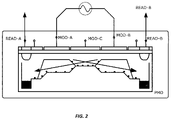
- FIG. 2 illustrates an example photonic mixing device (PMD).
- FIG. 3 is a diagram illustrating principles of phase measurement according to time-of-flight (TOF) techniques.
- FIG. 4 is a schematic diagram illustrating an example arrangement of pixels and read-out circuitry.
- FIG. 6 is a block diagram illustrating components of an example image processing system, according to some embodiments.
- image and image sensor are not limited to images or sensors involving visible light but encompass the use of visible light and other electromagnetic radiation.
- light as used herein is meant broadly and refers to visible light as well as infrared and ultraviolet radiation.
- FIG. 1 illustrates the basic principles of continuous-wave (CW) time-of-flight (TOF) measurements, which are well known.
- a light source 110 such as a light-emitting diode (LED) or vertical-cavity surface-emitting laser (VCSEL), is modulated with an electrical signal (e.g., a radio-frequency sinusoid at, for example, 300 MHz), so that the light source 110 emits an amplitude-modulated optical signal towards the target scene 120 .
- an electrical signal e.g., a radio-frequency sinusoid at, for example, 300 MHz
- the light signal reflects from an object or objects in the scene 120 and arrives back at a pixel array 135 in the TOF sensor 130 , with the time of flight to the target scene 120 and back imposing a phase shift of ⁇ on the optical signal as received at the pixel array 135 , relative to the originally transmitted optical signal.
- the modulation signal 137 used to modulate the emitted light, or a phase-shifted version of it, is also supplied as a reference signal to the pixels in pixel array 135 , to be correlated with the modulation signal superimposed on the reflected optical signal—in effect, the reflected optical signal is demodulated by each pixel in the pixel array 135 .
- each of the pixels in pixel array 135 may in some instances be a photon mixing device, or PMD.
- FIG. 2 illustrates the basic structure of an example PMD, which includes readout diodes A and B and modulation gates A and B.
- a reference signal is applied differentially across the modulation gates A and B, creating a gradient in electric potential across the p-substrate, while incoming light is received at a photo gate/diode.
- a differential sensor signal is generated across the readout diodes A and B. The sensor signal from a pixel may be integrated for a period of time to determine phase measurement information.
- the difference between voltages at the Read-A and Read-B nodes of the PMD corresponds to the correlation between the modulated optical signal detected by the photosensitive diode structures in the illustrated device and the reference signal, which is applied between the Mod-A and Mod-B nodes of the device.
- the PMD demodulate the modulated optical signal reflected from the target scene 120 , producing a pixel signal value (in this case the difference between voltages at Read-A and Read-B) indicative of the distance traveled by the reflected optical signal, as discussed in further detail below.
- r ⁇ ( ⁇ ) ( a 2 ) ⁇ cos ⁇ ( ⁇ + w ⁇ ⁇ ⁇ ) , which is a function of the phase difference ⁇ between the two signals. It will be appreciated that with a periodic modulation signal, this correlation can be carried out for an extended period of time, e.g., several cycles of the modulating signal, to improve the signal-to-noise ratio of the resulting measurement.
- the phase difference between the emitted optical signal and the received reflection of that signal can be extracted by an N-phase shifting technique.
- This requires sampling the correlation function at N different points, e.g., by performing correlations using N different phase shifts of the reference signal, with respect to the modulating signal g(t). At least two measurements are required to calculate this phase shift, and hence to determine the distance traveled. This is often done using four different phase shifts, at 0, 90, 180, and 270 degrees, as this allows for a simple cancellation of systematic offsets in the correlation results. This is seen in FIG.
- phase ⁇ which shows how the correlations A 0 and A 1 , at 0 and 90 degrees, respectively, correspond to a first phase vector having an “ideal” component corresponding to the actual difference traveled by the optical signal and a systematic component reflecting systematic error in the measurements and readout.
- the correlations A 2 and A 3 at 180 and 270 degrees, respectively, correspond to a second phase vector pointing in the opposite direction, with an exactly opposite “ideal” component and an identical systematic component.
- the ideal components are represented by the vectors extending from the origin to the circle, while the systematic error components are represented by the smaller vectors.
- the actual phase ⁇ can then be calculated as follows:
- the distance, or “depth” to the target scene 120 can be calculated as follows:
- phase measurements are commonly made for each pixel of the pixel array 135 , and combined, e.g., as shown in the phase calculation above, to result in a single distance measurement for each pixel.
- the resulting array of distance measurements thus forms a “depth map” mapping the distances between the pixels and the object or objects in the illuminated scene.
- the accuracy provided by four or more phase measurements per depth value is not always necessary.
- the use of several measurements per depth map is expensive, in terms of memory usage and processing resources, as the pixel signal value for each pixel in the pixel array 135 must be read from the array and stored several times, with each of these read-outs corresponding to a so-called exposure of the pixel array 135 , before being combined into depth map values.
- Embodiments of the techniques and devices detailed below address this problem by providing a technique whereby a pixel array is subjected to two (or more) exposures, corresponding to two (or more) phases of the reference signal, relative to the modulated optical signal emitted by the TOF device, but where the pixel signal values are read-out only a single time, reducing memory demands.
- the technique can be extended to three, four, or more exposures.
- the entire pixel array is subjected to a first exposure to the reflected optical signal, with a first phase setting for the reference signal, relative to the signal used to modulate the transmitted optical signal.
- every second line of pixels is set into a “hold” state, such that it retains the pixel signal value, i.e., the demodulated output representing the correlation between the modulation on the received optical signal and the reference signal.
- Pixels in a typical pixel array already have this hold state, but, typically, the hold signal is globally applied to all pixels, such that all pixels are in the hold state, or not.
- the result is an array of pixels which alternately store, from one line to the next, the result of the first or the second measurement.
- the array can then be read out a single time, effectively providing two phase measurements in one readout.
- a distance calculation can be done on the sensor, by combining two neighboring pixels, so as to produce a half-resolution depth map from a single readout of the pixel array.
- this approach it is possible to do a dual-exposure, single-readout measurement, with an on-chip distance calculation that does not require the involvement of an off-board application processor.
- this may be a special mode of operation, with reduced accuracy compared to a traditional nine-phase measurement, but with significantly reduced power consumption.
- the two-exposure approach described above can be generalized to three or more exposures. More generally, the presently described techniques include controlling the pixels of an image sensor so that the pixel signal values captured by a first subset of the pixels during the first exposure are held, during one or more subsequent exposures that generate new pixel signal values for the remaining subset of pixels. Subsequently, the pixel signal values for all of the pixels can be read in a single read-out of the pixel array, with the first subset yielding pixel signal values corresponding to the first exposure, and hence the first phase of the reference signal, and the remaining pixels yielding pixel signal values corresponding to the second (or subsequent) exposure, and hence the second (or other) phase of the reference signal.
- the second subset (and any additional subsets) of pixels may generate pixel signal values during the first exposure, with these pixel signal values effectively being discarded during the second exposure.
- the second subset of pixels in these embodiments operate normally during the first exposure, with their output values being replaced by values from the second exposure before being read.
- the second subset of pixels may be deactivated or be otherwise configured to not generate pixel signal values during the first exposure.
- first and second (and any additional) subsets of pixels may comprise all of the pixels of an image sensor or imaging device, in some embodiments, while comprising only some of the pixels of the sensor or imaging device, in others.
- a first portion of a device's pixels may be controllable according to the techniques described herein, while a second portion of the device's pixels are configured for operation according to conventional techniques.
- the first subset of pixels corresponds to every second row in an array of pixels having rows and columns.
- each pixel in this first subset produces a pixel signal value corresponding to the first exposure, while its closest neighboring pixel in an adjacent row produces a pixel signal value corresponding to the second exposure.
- the first and second exposures correspond to a 90-degree difference in the respective reference signal phases, the pixel signal value for each pixel in the first subset can be immediately combined with the pixel signal value for its neighboring pixel in the adjacent row, e.g., according to
- this calculation is performed by logic implemented directly on the same chip incorporating the pixel array, and can be implemented so as to further reduce storage/memory requirements.
- FIG. 4 is a schematic diagram illustrating elements of an example image processing system incorporating aspects of the techniques discussed above. It should be understood that FIG. 4 includes a simplified drawing of a pixel array, only illustrating four lines of pixels of what may be a much larger array of pixels, together with a subset of the corresponding readout circuitry. Furthermore, it should be understood that the illustrated pixels are not PMD pixels, but standard pixels, to simplify the drawing. However, the concept can be directly applied to PMD pixels or to other pixel structures that demodulate a modulated light signal so as to produce a correlation between the modulation on the light signal and a reference signal provided to the pixels.
- the lines extending into the pixel array from the left side are the hold lines.
- the hold lines for all rows are connected to a single global hold signal, which controls the hold switches of all the pixels synchronously.
- the global hold signal is split in two, such that neighboring rows of pixels can be controlled independently. This has no effect on the pixel array itself—only the distribution of the control signals outside the array needs to be modified, compared to conventional pixel array structures.
- row_ 0 there are also so-called row-select signals, labeled row_ 0 , row_ 1 , row_ 2 and row_ 3 in the figure.
- row_select signals labeled row_ 0 , row_ 1 , row_ 2 and row_ 3 in the figure.
- ADCs analog-to-digital converters
- FIG. 4 When analog to digital conversion of the selected row is finished, the next row is selected, and so on.
- ADCs analog-to-digital converters
- the illustrated implementation uses 16 ADCs, with the 224 columns in this example circuit being divided into groups of 14. With this approach, 16 columns at a time are read, and only 14 sequential read operations.
- two blocks of pixel memory are used in ping-pong operation. While the ADC is converting one line of pixels and storing the data in one of the memory blocks, a high-speed data interface (not shown) transfers data from the other memory block to the application processor. When both of these processes are finished (conversion of one line and transmission of another line), the operation switches, meaning that the data which have just been generated in the one memory block is now transferred via the interface and the other memory block is used for conversion.
- logic for calculating an arctangent (ATAN) from two pixel signal values before transmission is added.
- ATAN arctangent
- this may be implemented on the same integrated circuit device that carries the array of pixels, i.e., as a function that is “on-board” the image sensor device rather than in a separate processor.
- Implementation of an ATAN function can be done using very efficiently, using algorithms like the so-called “CORDIC” algorithm. It will be appreciated that this further reduces the memory requirements—with this approach, a first row of pixel signal values is read from the pixel signal array, converted into digital form, and stored in pixel memory.
- half-resolution depth map values are directly delivered by the pixel array circuit to an off-board memory, in some embodiments.
- FIG. 5 illustrates an example method for processing pixel signal values from an image sensor having a plurality of pixels, where each pixel is configured to generate a respective pixel signal value by demodulating received light using a reference signal.
- the method includes controlling at least a first subset of the plurality of pixels to generate respective pixel signal values, based on a first reference signal applied to (at least) the first subset of the pixels, for a first exposure.
- the first subset of the plurality of pixels to are then controlled to hold their respective pixel signal values.
- pixel signal values are generated for all of the pixels of the pixel array during this first exposure, but the pixel measurements for pixels other than the first subset are not maintained—i.e., these pixel signal values are not “held” after the first measurement.
- a second subset of the plurality of pixels are controlled to generate respective pixel signal values, based on a second reference signal applied to (at least) the second subset of the pixels. This is illustrated in block 530 . As shown at block 540 , this second subset of the plurality of pixels are then controlled to hold their respective pixel signal values.
- the first reference signal may have a first phase, relative to a modulating signal applied, during the first exposure, to an optical signal being measured by the image sensor, while the second reference signal, which may otherwise be identical to the first reference signal, has a second phase, relative to the modulating signal applied, during the second exposure, to the optical signal being measured by the image sensor.
- this difference in phase between the first and second reference signals may be generated by introducing a phase shift to an input reference signal, between the first and second exposures, or by introducing a phase shift to the modulating signal applied to the optical signal under measurement, between the first and second exposures, or by a combination of both.
- this technique can be extended to a third, fourth, or more subsets of pixels, corresponding to respective third, fourth, and subsequent phases.
- the illustrated method further comprises subsequently reading out the pixel signal values from (at least) the first and second subsets of the plurality of pixels and converting the read pixel signal values to digital pixel values, as shown at block 550 .
- the image sensor may, in some embodiments, have further pixels, in addition to those that are controlled according to the techniques described herein.
- the plurality of pixels are arranged in an array having lines and columns, e.g., where the first subset of pixels comprises pixels in every odd or even line of the array and the second subset of pixels comprises the remaining pixels.
- this makes it especially convenient to perform on-board phase calculations, using neighboring pixels that correspond to different exposures with different phases for the reference signals applied during the exposures.
- the method may further include generating depth values for a depth map by combining, for each depth value, a digital pixel value for a pixel of the first subset with a digital pixel value for a corresponding pixel of the second subset. This is shown at block 560 of FIG.
- the plurality of pixels are arranged in an array having lines and columns, the first subset of pixels comprising pixels in every odd or even line of the array and the second subset of pixels comprising the remaining pixels, and wherein said combining comprises, for each depth value, combining a digital pixel value for a pixel in any given line with the digital pixel value for the neighboring pixel in an immediately adjacent line.
- the difference between the phase of the first reference signal and the phase of the second reference signal, relative to the signal modulating the optical signal under measurement is 90 degrees, in which case said combining may comprise computing an arctangent of a ratio of the digital pixel values for the pixels.
- FIG. 6 correspondingly, illustrates an example image processing system 600 , according to several embodiments of the presently disclosed devices and systems.
- the system 600 can be utilized to detect objects, e.g., as shown in target scene 602 , as well as to determine distances to the detected objects.
- System 600 may be a continuous-wave TOF system, such as a photon modulation device (PMD)-based TOF system.
- PMD photon modulation device
- the illustrated system 600 includes a light source 624 , which is configured to amplitude modulate a beam of light and emit the amplitude-modulated light towards the scene 602 .
- the amplitude modulation may be based on a reference signal generated by reference signal generator 608 .
- the reference signal may be a radio-frequency (RF) signal, e.g., in the MHz range, although other modulation frequencies can be used.
- RF radio-frequency
- the emitted light can include light having varied ranges of wavelength, such as sunlight and infra-red. The emitted light reflects from one or more objects in the scene and returns to the sensor 604 .
- Image process system 600 may be configured to carry out a technique whereby a first exposure obtains pixel measurements for at least a first subset of the pixels of a pixel array at a single interval of time, for a particular phase shift of the reference signal, relative to a signal modulating the optical signal under measurement. For a second exposure, each of the first subset of the pixels is set to a “hold” state, so that the values obtained from the first measurement are maintained. This first subset may be, for example, every second line of the pixel array. In some embodiments, pixel measurements are obtained for all of the pixels of the pixel array during the first measurement/exposure, but the pixel measurements for pixels other than the first subset are not maintained—i.e., these pixels are not “held” after the first measurement.
- a second exposure, using a different phase is performed for a second subset of the pixels, e.g., all of those pixels that were not set to the hold state after the first exposure.
- the result of this process is an array of pixels in which the first subset of pixels holds the results of the first exposure, while the second subset of pixels holds the results of the second exposure.
- These pixel values can be read out all at once, after the second exposure, with certain calculations being performed directly, as the pixel values are read from the pixel array.
- This approach can dramatically reduce the need for data storage, as separate memory for storing pixel values between exposures is not needed. Further, this approach can simplify the processing requirements for generating a depth map, as an on-chip distance calculation can be performed between neighboring pixels as the pixel values are read from the array. Thus, memory, complexity, and power consumption are reduced.
- the illustrated image processing system 600 includes a sensor 604 , which comprises a plurality of pixels configured to generate a respective plurality of pixel signal values in response to received light 614 , where each pixel is configured to obtain its respective pixel signal value by demodulating received light using a reference signal 622 .
- received light 602 may be reflected from a target scene 602 .
- one suitable pixel design is the PMD described above.
- the numbers of pixels, rows, and columns can vary, from one embodiment to another, and are selected based on factors including desired resolution, intensity, and the like. In one example, these sensor characteristics are selected based on the objects to be detected and the expected distances to the objects. Thus, for example, the pixel resolution of the pixels in sensor 604 may vary, from one embodiment to another. Small objects require a higher resolution for detection. For example, finger detection requires a resolution of ⁇ 5 mm per pixel at a distance or range of about 0.5 meters. Medium sized objects, such as hand detection, require a resolution of ⁇ 20 mm per pixel at a range of about 1.5 meters. Larger sized objects, such as a human body, require a resolution of ⁇ 60 mm per pixel at about 2.5 meters.
- Image processing system 600 further includes a reference signal generator 608 , which may be configured, in some embodiments, to generate reference signal 622 with a selectable phase, relative to the phase of a modulation signal applied to light transmitted towards target scene 602 , and to provide the reference signal 622 to the plurality of pixels in sensor 604 .
- Image processing system 600 still further includes an analog-to-digital converter (ADC) circuit 606 , which may include one or several ADCs, operatively coupled to the plurality of pixels in sensor 604 .
- ADC analog-to-digital converter
- the illustrated image processing system 600 further includes control circuitry 612 , which may comprise, for example a processor, controller, or the like, and/or other digital logic.
- the control circuitry 612 is configured to cause the image processing system 600 to carry out a method like those described above, in connection with FIG. 5 .
- control circuity 612 may be configured to control the reference signal generator 608 to generate a first reference signal, and to control at least a first subset of the plurality of pixels in sensor 604 to generate respective pixel signal values, based on the first reference signal, for a first exposure.
- Control circuitry 612 is further configured to, subsequent to the first exposure, control the first subset of the plurality of pixels to hold their respective pixel signal values, and to then control the reference signal generator 608 to generate a second reference signal, while the first subset of the plurality of pixels are holding their respective pixel signal values.
- the control circuitry 612 is configured to generate the first reference signal so that it has a first phase, relative to a modulating signal applied, during the first exposure, to an optical signal being measured by the image sensor, and to generate the second reference signal so that it has a second phase, relative to the modulating signal applied, during the second exposure, to the optical signal being measured by the image sensor. This may be done, for example, by introducing a phase shift to an input reference signal, between the first and second exposures, at a point before the reference signal is applied to the pixels.
- Control circuitry 612 in these embodiments is still further configured to, while the first subset of the plurality of pixels continue to hold their respective pixel signal values, control a second subset of the plurality of pixels to generate respective pixel signal values, based on the second reference signal, for a second exposure, and then subsequent to the second exposure, control the second subset of the plurality of pixels to hold their respective pixel signal values.
- control circuitry 612 is configured to read out the pixel signal values, as shown at signal 618 in FIG. 6 , for conversion to respective digital pixel values by the ADC circuit 606 .
- the plurality of pixels in sensor 604 may be arranged in an array having lines and columns, where the first subset of pixels comprises pixels in every odd or even line of the array and the second subset of pixels comprises the remaining pixels.
- the image processing system 600 may further include calculating logic, represented in FIG. 6 by depth map generator 610 , configured to generate depth values for a depth map by combining, for each depth value, a digital pixel value for a pixel of the first subset with a digital pixel value for a corresponding pixel of the second subset.
- the calculating logic may be configured to, for each depth value, combine a digital pixel value for a pixel in any given line with the digital pixel value for the neighboring pixel in an immediately adjacent line.
- the difference between the phase of the first reference signal and the phase of the second reference signal, relative to a signal modulating the optical signal under measurement may be 90 degrees, for example, where the calculating logic is configured to combine digital pixel values by computing an arctangent of a ratio of the digital pixel values for the pixels.
- image processing system 600 comprises a memory operatively coupled to the ADC circuit 606 , e.g., as part of depth map generator 610 , and configured to store digital pixel values for one line of the array at a time, where the calculating logic is configured to compute each arctangent using a digital pixel value stored in the memory and a corresponding digital pixel value for the neighboring pixel in the immediately adjacent line.
- system 600 may be used for low power applications and modes, to mitigate power consumption. However, it is appreciated that the system 600 can be used for other applications and modes. It is also appreciated that variations in the components of the system 100 are contemplated, including additional components and/or omission of shown components.
- the system 600 uses the combined pixels, as described above to generate a depth map in the low power mode.
- the same system 600 may use multiple exposures to obtain a higher resolution depth map.
- the system 600 can selectively switch between the mode using combined pixels and the mode using multiple exposures to obtain a higher resolution.
- the mode using combined pixels may be a low power mode with a lower resolution when compared to the multiple exposure mode or approach.
- the system 600 may be capable to roughly calculate 3D data directly on the sensor chip without the need for data processing external to the sensor chip, since as discussed above, a rough distance calculation can be performed using only a simple arctan calculation. Such a calculation may be implemented fully in hardware directly on the sensor chip using gates and/or other logic available in hardware.
- the combined pixel mode may allow determining 3D data fully on the sensor chip without external calculator devices.
- the system 600 in some embodiments can switch from the lower power mode described herein to a higher resolution mode based on a number of factors or conditions.
- the low-power mode is also referred to as a low-resolution mode.
- a touchless gesture control system can use the lower power mode initially and switch to the higher resolution mode once activity is detected to enable more precise measurements.
- Another example is face detection, where the lower power mode is used for shape detection. Once a shape is detected, the system switches to higher resolution mode to measure facial features.
- Other variations and uses are also contemplated for the system 600 .
- the claimed subject matter may be implemented as a method, apparatus, or article of manufacture using standard programming and/or engineering techniques to produce software, firmware, hardware, or any combination thereof to control a computer to implement the disclosed subject matter.
- article of manufacture as used herein is intended to encompass a computer program accessible from any computer-readable device, carrier, or media.
Landscapes
- Engineering & Computer Science (AREA)
- Physics & Mathematics (AREA)
- Computer Networks & Wireless Communication (AREA)
- General Physics & Mathematics (AREA)
- Radar, Positioning & Navigation (AREA)
- Remote Sensing (AREA)
- Electromagnetism (AREA)
- Multimedia (AREA)
- Signal Processing (AREA)
- Optical Radar Systems And Details Thereof (AREA)
Abstract
Description
m(t)=cos (ωt), and
s(t)=1+(a×cos (ωt+∅)),
then the correlation of the received signal with the reference signal gives:
which is a function of the phase difference ∅ between the two signals. It will be appreciated that with a periodic modulation signal, this correlation can be carried out for an extended period of time, e.g., several cycles of the modulating signal, to improve the signal-to-noise ratio of the resulting measurement.
where fmod is the frequency of the modulating signal. It will be appreciated that because of “phase wrapping,” this distance calculation has an ambiguous result, as it is not possible to tell from a single distance calculation whether the distance traveled is less than a single wavelength of the modulating waveform, or multiple wavelengths. Various techniques for resolving this ambiguity are well known, e.g., by incorporating amplitude information obtained from the reflected optical signal, and/or repeating the measurement with a different modulating frequency, but a detailed discussion of these techniques is unnecessary to a full understanding of the presently disclosed techniques and is thus beyond the scope of the present disclosure.
to obtain a phase value, for direct application to a depth map. As also discussed in further detail below, in some embodiments of the devices disclosed herein, this calculation is performed by logic implemented directly on the same chip incorporating the pixel array, and can be implemented so as to further reduce storage/memory requirements.
Claims (14)
Priority Applications (3)
| Application Number | Priority Date | Filing Date | Title |
|---|---|---|---|
| US16/176,817 US11506763B2 (en) | 2018-10-31 | 2018-10-31 | Image sensor with interleaved hold for single-readout depth measurement |
| CN201911046732.3A CN111200710A (en) | 2018-10-31 | 2019-10-30 | Image sensor with interleaved hold for single readout depth measurement |
| EP19206585.2A EP3647813A1 (en) | 2018-10-31 | 2019-10-31 | Image sensor with interleaved hold for single-readout depth measurement |
Applications Claiming Priority (1)
| Application Number | Priority Date | Filing Date | Title |
|---|---|---|---|
| US16/176,817 US11506763B2 (en) | 2018-10-31 | 2018-10-31 | Image sensor with interleaved hold for single-readout depth measurement |
Publications (2)
| Publication Number | Publication Date |
|---|---|
| US20200132819A1 US20200132819A1 (en) | 2020-04-30 |
| US11506763B2 true US11506763B2 (en) | 2022-11-22 |
Family
ID=68426120
Family Applications (1)
| Application Number | Title | Priority Date | Filing Date |
|---|---|---|---|
| US16/176,817 Active 2041-04-29 US11506763B2 (en) | 2018-10-31 | 2018-10-31 | Image sensor with interleaved hold for single-readout depth measurement |
Country Status (3)
| Country | Link |
|---|---|
| US (1) | US11506763B2 (en) |
| EP (1) | EP3647813A1 (en) |
| CN (1) | CN111200710A (en) |
Cited By (1)
| Publication number | Priority date | Publication date | Assignee | Title |
|---|---|---|---|---|
| US20210405166A1 (en) * | 2020-06-08 | 2021-12-30 | Shenzhen GOODIX Technology Co., Ltd. | Time-of-flight based distance measuring method and related distance measuring system |
Families Citing this family (4)
| Publication number | Priority date | Publication date | Assignee | Title |
|---|---|---|---|---|
| CN111398979B (en) * | 2020-06-08 | 2020-10-16 | 深圳市汇顶科技股份有限公司 | Ranging method based on flight time and related ranging system |
| CN114071040B (en) * | 2020-07-31 | 2024-11-05 | 宁波飞芯电子科技有限公司 | Image sensor and method for reading out signal |
| US20240319373A1 (en) * | 2023-03-20 | 2024-09-26 | Analog Devices International Unlimited Company | Continuous wave time of flight system |
| US20240319372A1 (en) * | 2023-03-20 | 2024-09-26 | Javier CALPE | Continuous wave time of flight system |
Citations (8)
| Publication number | Priority date | Publication date | Assignee | Title |
|---|---|---|---|---|
| US20060128087A1 (en) * | 2000-11-09 | 2006-06-15 | Canesta, Inc. | Methods and devices for improved charge management for three-dimensional and color sensing |
| US20110129123A1 (en) | 2009-11-27 | 2011-06-02 | Ilia Ovsiannikov | Image sensors for sensing object distance information |
| DE102013208805A1 (en) * | 2012-05-30 | 2013-12-05 | Pmdtechnologies Gmbh | Method for operating PMD sensor of PMD camera, involves buffering propagation time relevant signals of pixel block in selection circuits associated with receiving frames and reading propagation time relevant signals in end of sequence |
| EP2894492A1 (en) | 2014-01-13 | 2015-07-15 | Softkinetic Sensors N.V. | A method for driving a time-of-flight system |
| US20160327638A1 (en) * | 2015-05-04 | 2016-11-10 | Infineon Technologies Ag | Systems and methods for time of flight measurement using a single exposure |
| US20180259628A1 (en) | 2017-03-10 | 2018-09-13 | Infineon Technologies Ag | Time of flight imaging apparatuses and a method for adjusting a reference frequency |
| US20180295274A1 (en) | 2015-12-16 | 2018-10-11 | Nikon Corporation | Image-capturing apparatus and motion detection method |
| US20190056498A1 (en) * | 2016-03-01 | 2019-02-21 | Brightway Vision Ltd. | Gated imaging apparatus, system and method |
Family Cites Families (7)
| Publication number | Priority date | Publication date | Assignee | Title |
|---|---|---|---|---|
| US7855740B2 (en) * | 2007-07-20 | 2010-12-21 | Eastman Kodak Company | Multiple component readout of image sensor |
| JP6293134B2 (en) * | 2012-07-09 | 2018-03-14 | ブライトウェイ ビジョン リミテッド | Stereo-gated image system and method |
| JP6286677B2 (en) * | 2013-06-26 | 2018-03-07 | パナソニックIpマネジメント株式会社 | Ranging system and imaging sensor |
| CN105452807A (en) * | 2013-08-23 | 2016-03-30 | 松下知识产权经营株式会社 | Distance measurement system and signal generation device |
| US10191154B2 (en) * | 2016-02-11 | 2019-01-29 | Massachusetts Institute Of Technology | Methods and apparatus for time-of-flight imaging |
| US9843746B2 (en) * | 2016-05-03 | 2017-12-12 | Altasens, Inc. | Image sensor combining high dynamic range techniques |
| US11448757B2 (en) * | 2016-11-29 | 2022-09-20 | Nuvoton Technology Corporation Japan | Distance measuring device |
-
2018
- 2018-10-31 US US16/176,817 patent/US11506763B2/en active Active
-
2019
- 2019-10-30 CN CN201911046732.3A patent/CN111200710A/en active Pending
- 2019-10-31 EP EP19206585.2A patent/EP3647813A1/en not_active Ceased
Patent Citations (8)
| Publication number | Priority date | Publication date | Assignee | Title |
|---|---|---|---|---|
| US20060128087A1 (en) * | 2000-11-09 | 2006-06-15 | Canesta, Inc. | Methods and devices for improved charge management for three-dimensional and color sensing |
| US20110129123A1 (en) | 2009-11-27 | 2011-06-02 | Ilia Ovsiannikov | Image sensors for sensing object distance information |
| DE102013208805A1 (en) * | 2012-05-30 | 2013-12-05 | Pmdtechnologies Gmbh | Method for operating PMD sensor of PMD camera, involves buffering propagation time relevant signals of pixel block in selection circuits associated with receiving frames and reading propagation time relevant signals in end of sequence |
| EP2894492A1 (en) | 2014-01-13 | 2015-07-15 | Softkinetic Sensors N.V. | A method for driving a time-of-flight system |
| US20160327638A1 (en) * | 2015-05-04 | 2016-11-10 | Infineon Technologies Ag | Systems and methods for time of flight measurement using a single exposure |
| US20180295274A1 (en) | 2015-12-16 | 2018-10-11 | Nikon Corporation | Image-capturing apparatus and motion detection method |
| US20190056498A1 (en) * | 2016-03-01 | 2019-02-21 | Brightway Vision Ltd. | Gated imaging apparatus, system and method |
| US20180259628A1 (en) | 2017-03-10 | 2018-09-13 | Infineon Technologies Ag | Time of flight imaging apparatuses and a method for adjusting a reference frequency |
Non-Patent Citations (1)
| Title |
|---|
| DE-102013208805 translation 2013. * |
Cited By (1)
| Publication number | Priority date | Publication date | Assignee | Title |
|---|---|---|---|---|
| US20210405166A1 (en) * | 2020-06-08 | 2021-12-30 | Shenzhen GOODIX Technology Co., Ltd. | Time-of-flight based distance measuring method and related distance measuring system |
Also Published As
| Publication number | Publication date |
|---|---|
| US20200132819A1 (en) | 2020-04-30 |
| EP3647813A1 (en) | 2020-05-06 |
| CN111200710A (en) | 2020-05-26 |
Similar Documents
| Publication | Publication Date | Title |
|---|---|---|
| US11506763B2 (en) | Image sensor with interleaved hold for single-readout depth measurement | |
| US9971023B2 (en) | Systems and methods for time of flight measurement using a single exposure | |
| US11668829B2 (en) | Resolving distance measurement ambiguities using coded-modulation phase image frames | |
| US10830579B2 (en) | Three-dimensional triangulational scanner having high dynamic range and fast response | |
| CN111308482B (en) | Filtered Continuous Wave Time-of-Flight Measurement Based on Coded Modulated Images | |
| US12204052B2 (en) | Phase noise and methods of correction in multi-frequency mode lidar | |
| CN111045029B (en) | Fused depth measuring device and measuring method | |
| US8629976B2 (en) | Methods and systems for hierarchical de-aliasing time-of-flight (TOF) systems | |
| US11874403B2 (en) | Reflectance sensing with time-of-flight cameras | |
| CN112135114B (en) | Time-of-Flight Image Sensor Resolution Enhancement and Increased Data Robustness Using Merging Modules | |
| WO2016186775A1 (en) | Gated time of flight camera | |
| WO2019146457A1 (en) | Time-of-flight image sensor with distance determination | |
| EP1752793A1 (en) | Method and device for redundant distance measurement and mismatch cancellation in phase-measurement systems | |
| EP3602110B1 (en) | Time of flight distance measurement system and method | |
| US11681025B2 (en) | Simultaneous data transmission and depth image recording with time-of-flight cameras | |
| US11467264B2 (en) | Apparatus for measuring depth with pseudo 4-tap pixel structure | |
| Jongenelen et al. | Efficient FPGA implementation of homodyne-based time-of-flight range imaging | |
| CN112817002A (en) | Distance detection system and image acquisition module comprising same | |
| US20230335027A1 (en) | Method and arrangements for provision of pixel values for readout from an image sensor |
Legal Events
| Date | Code | Title | Description |
|---|---|---|---|
| FEPP | Fee payment procedure |
Free format text: ENTITY STATUS SET TO UNDISCOUNTED (ORIGINAL EVENT CODE: BIG.); ENTITY STATUS OF PATENT OWNER: LARGE ENTITY |
|
| AS | Assignment |
Owner name: INFINEON TECHNOLOGIES AG, GERMANY Free format text: ASSIGNMENT OF ASSIGNORS INTEREST;ASSIGNORS:DIELACHER, MARKUS;FLATSCHER, MARTIN;LOBNIK, ROBERT;AND OTHERS;REEL/FRAME:047587/0669 Effective date: 20180511 |
|
| AS | Assignment |
Owner name: INFINEON TECHNOLOGIES AG, GERMANY Free format text: CORRECTIVE ASSIGNMENT TO CORRECT THE EXECUTION DATE FOR ALL INVENTORS PREVIOUSLY RECORDED AT REEL: 47587 FRAME: 669. ASSIGNOR(S) HEREBY CONFIRMS THE ASSIGNMENT;ASSIGNORS:DIELACHER, MARKUS;FLATSCHER, MARTIN;LOBNIK, ROBERT;AND OTHERS;REEL/FRAME:048107/0150 Effective date: 20181105 |
|
| STPP | Information on status: patent application and granting procedure in general |
Free format text: NON FINAL ACTION MAILED |
|
| STPP | Information on status: patent application and granting procedure in general |
Free format text: RESPONSE TO NON-FINAL OFFICE ACTION ENTERED AND FORWARDED TO EXAMINER |
|
| STPP | Information on status: patent application and granting procedure in general |
Free format text: FINAL REJECTION MAILED |
|
| STPP | Information on status: patent application and granting procedure in general |
Free format text: RESPONSE AFTER FINAL ACTION FORWARDED TO EXAMINER |
|
| STPP | Information on status: patent application and granting procedure in general |
Free format text: NOTICE OF ALLOWANCE MAILED -- APPLICATION RECEIVED IN OFFICE OF PUBLICATIONS |
|
| STCF | Information on status: patent grant |
Free format text: PATENTED CASE |
|
| CC | Certificate of correction |