US11506714B2 - Setup time and hold time detection system and detection method - Google Patents

Setup time and hold time detection system and detection method Download PDF

Info

Publication number
US11506714B2
US11506714B2 US17/448,703 US202117448703A US11506714B2 US 11506714 B2 US11506714 B2 US 11506714B2 US 202117448703 A US202117448703 A US 202117448703A US 11506714 B2 US11506714 B2 US 11506714B2
Authority
US
United States
Prior art keywords
circuit
time
setup
test circuits
hold
Prior art date
Legal status (The legal status is an assumption and is not a legal conclusion. Google has not performed a legal analysis and makes no representation as to the accuracy of the status listed.)
Active
Application number
US17/448,703
Other versions
US20220326304A1 (en
Inventor
Shih-Hao Chen
Chih-Wen Yang
Current Assignee (The listed assignees may be inaccurate. Google has not performed a legal analysis and makes no representation or warranty as to the accuracy of the list.)
Digwise Technology Corp Ltd
Original Assignee
Digwise Technology Corp Ltd
Priority date (The priority date is an assumption and is not a legal conclusion. Google has not performed a legal analysis and makes no representation as to the accuracy of the date listed.)
Filing date
Publication date
Application filed by Digwise Technology Corp Ltd filed Critical Digwise Technology Corp Ltd
Assigned to DIGWISE TECHNOLOGY CORPORATION, LTD reassignment DIGWISE TECHNOLOGY CORPORATION, LTD ASSIGNMENT OF ASSIGNORS INTEREST (SEE DOCUMENT FOR DETAILS). Assignors: CHEN, SHIH-HAO, YANG, CHIH-WEN
Publication of US20220326304A1 publication Critical patent/US20220326304A1/en
Application granted granted Critical
Publication of US11506714B2 publication Critical patent/US11506714B2/en
Active legal-status Critical Current
Anticipated expiration legal-status Critical

Links

Images

Classifications

    • GPHYSICS
    • G01MEASURING; TESTING
    • G01RMEASURING ELECTRIC VARIABLES; MEASURING MAGNETIC VARIABLES
    • G01R31/00Arrangements for testing electric properties; Arrangements for locating electric faults; Arrangements for electrical testing characterised by what is being tested not provided for elsewhere
    • G01R31/28Testing of electronic circuits, e.g. by signal tracer
    • G01R31/317Testing of digital circuits
    • G01R31/3181Functional testing
    • G01R31/319Tester hardware, i.e. output processing circuits
    • G01R31/3193Tester hardware, i.e. output processing circuits with comparison between actual response and known fault free response
    • G01R31/31937Timing aspects, e.g. measuring propagation delay
    • HELECTRICITY
    • H01ELECTRIC ELEMENTS
    • H01LSEMICONDUCTOR DEVICES NOT COVERED BY CLASS H10
    • H01L22/00Testing or measuring during manufacture or treatment; Reliability measurements, i.e. testing of parts without further processing to modify the parts as such; Structural arrangements therefor
    • H01L22/10Measuring as part of the manufacturing process
    • H01L22/14Measuring as part of the manufacturing process for electrical parameters, e.g. resistance, deep-levels, CV, diffusions by electrical means
    • H10P74/207

Definitions

  • the present disclosure relates to a setup time and hold time detection system and detection method, especially used to detect the setup time and hold time of a circuit during signal transmission.
  • semiconductor elements are also more sensitive to voltage and temperature. Therefore, in order to ensure the defect rate and performance of the semiconductor product, semiconductor elements must be tested, especially for the timing errors of semiconductor elements.
  • One aspect of the present disclosure is a setup time and hold time detection system, comprising a monitoring unit and a processing unit.
  • the monitoring unit is electrically coupled to a plurality of test circuits, and is configured to detect a plurality of setup times and a plurality of hold times of the plurality of test circuits during signal transmission according to a source clock signal.
  • the processing unit is electrically coupled the monitoring unit, and is configured to receive the plurality of setup times and the plurality of hold times.
  • the processing unit is configured to record the plurality of setup times and the plurality of hold times as a plurality of detection data of the plurality of test circuits.
  • the processing unit cormprises a data module circuit and a data detection circuit.
  • the data module circuit is configured to select a first part of the detection data as a plurality of first detection data to establish an estimation model.
  • the estimation model is configured to estimate a signal transmission status of the plurality of test circuits under different conditions.
  • the data detection circuit is configured to select a second part of the detection data as a plurality of second detection data.
  • the plurality of second detection data are different from the plurality of first detection data, and are configured to compare with a plurality of estimation results generated by the estimation model to obtain an error value of the estimation model.
  • a setup time and hold time detection method comprising the following steps: detecting, by a monitoring unit, a plurality of setup times of a plurality of test circuits and a plurality of hold times of the plurality of test circuits during signal transmission; recording the plurality of setup times and the plurality of hold times as a plurality of detection data of the plurality of test circuits; selecting a first part of the detection data as a plurality of first detection data, and establishing an estimation model according to the plurality of first detection data; selecting a second part of the detection data as a plurality of second detection data, wherein the plurality of second detection data are different from the plurality of first detection data; and comparing the plurality of second detection data with a plurality of estimation results generated by the estimation model to obtain an error value of the estimation model.
  • FIG. 1A is a schematic diagram of the detection system and the test circuits in some embodiments of the present disclosure.
  • FIG. 1B is a schematic diagram of the test chip in some embodiments of the present disclosure.
  • FIG. 1C is a time sequence of the signal in some embodiments of the present disclosure.
  • FIG. 2 is a schematic diagram of the detection system in some embodiments of the present disclosure.
  • FIG. 3A is a schematic diagram of the first monitoring circuit in some embodiments of the present disclosure.
  • FIG. 3B is a schematic diagram of the setup time in some embodiments of the present disclosure.
  • FIG. 3C is a schematic diagram of the second monitoring circuit in some embodiments of the present disclosure.
  • FIG. 3D is a schematic diagram of the hold time in some embodiments of the present disclosure.
  • FIG. 3E is a schematic diagram of the first monitoring circuit in some embodiments of the present disclosure.
  • FIG. 3F is a schematic diagram of the first monitoring circuit in some embodiments of the present disclosure.
  • FIG. 3G is a schematic diagram of the second monitoring circuit in some embodiments of the present disclosure.
  • FIG. 4A is a schematic diagram of the first monitoring circuit in some embodiments of the present disclosure.
  • FIG. 4B is a schematic diagram of the shift register in some embodiments of the present disclosure.
  • FIG. 4C is a schematic diagram of the register in some embodiments of the present disclosure.
  • FIG. 5A is a schematic diagram of the first monitoring circuit in some embodiments of the present disclosure.
  • FIG. 5B is a schematic diagram of the shift register in some embodiments of the present disclosure.
  • FIG. 5C is a schematic diagram of the register in some embodiments of the present disclosure.
  • FIG. 6 is a flowchart illustrating a detection method in some embodiments of the present disclosure.
  • the present disclosure relates to a setup time and hold time detection system and method applied in a test device, so as to detect operation status or operation parameters of the semiconductor elements in the test device during signal transmission.
  • the semiconductor elements can be a die on a wafer or a packaged chip.
  • the detection system is configured to perform a “functional parameter test” (or a dynamic function test) to detect the error of time sequence of each semiconductor element, but the present disclosure is not limited to this.
  • the test device has a huge number of the semiconductor elements to perform different logical operations. Since the configuration conditions of each the semiconductor elements are different, when the test device is operating, the operation status of each the semiconductor elements can not maintain within the ideal range. Therefore, it is necessary to confirm the true state of the semiconductor elements through detection to adjust or improve the manufacturing process.
  • the above “configuration conditions” include the structural characteristics, the arrang position, the ambient temperature or the stability of the power supply of the semiconductor elements, etc.
  • the width of the wire is compressed, resulting in an increase in resistance, so that the semiconductor elements will have an additional “IR drop (i.e., voltage drop)” that does not exist in an ideal state.
  • the size or magnitude of IR drop is related to a distance between the semiconductor elements and the I/O Pad of the test device.
  • the characteristics of voltage, current, temperature, etc. may also change, causing errors in the signal transmission of the semiconductor elements.
  • the detection system 100 includes multiple the monitors M and a processing unit 120 .
  • FIG. 1A is a schematic diagram of the detection system and the test circuits in some embodiments of the present disclosure.
  • the monitors M are arranged in the test device A 10 , and each of monitors M is electrically coupled to one test circuits A 11 in the test device A 10 .
  • test circuits A 11 can be the semiconductor elements discussed above.
  • FIG. 1A is a schematic diagram of the relative position between the monitors M and the test circuits A 11 , the internal circuit and detection methods will be detailed in following paragraphs.
  • the processing unit 120 is electrically coupled to registers REG of the test device A 10 .
  • the test circuits A 11 operates according to a test sample signal input from external device (i.e., Pattern provided by the processing unit 120 ), and stores the operated signal to the register REG by the monitor M.
  • the monitor M may detect the operation status and data of the corresponding test circuits A 11 , and transmits the detection result to the processing unit 120 by the registers REG.
  • FIG. 1B is a schematic diagram of the processing chip A 20 to be tested in the test device A 10 in some embodiments of the present disclosure.
  • the processing chip A 20 includes multiple circuits, and the processing chip A 20 has multiple areas with higher temperature during operation, which are called hot spots hit spots HS.
  • the circuit in the hot spot HS or the area adjacent to the hot spot HS is called the critical path or sub-critical path.
  • the circuit on the critical path or the sub-critical path is taken as the test circuits A 11 , but the present disclosure is not limited to this.
  • the monitor M is configured to detect “the error of the time sequence” of the test circuits A 11 .
  • the error of the time sequence means the relative relationship between the transmission time of a data signal and a source clock signal when the test circuits A 11 transmits the data dignal according to the source clock signal.
  • the error of the time sequence includes a setup time and a hold time.
  • FIG. 1C is a time sequence of the signal in some embodiments of the present disclosure.
  • the source clock signal CLK is configured to trigger the test circuits A 11 operateing (e.g., input or output).
  • the original data signal Sd is data/information that need to transmit to the test circuits A 11 .
  • the setup time is a time length that the original data signal Sd arrives in advance before the positive edge or the negative edge of the source clock signal CLK is arrived.
  • the hold time is a time length that the original data signal Sd maintains stable after the positive edge or the negative edge of the source clock signal CLK is arrived. For example, if the test circuits A 11 is triggered according to the positive edge (0 to 1) or the negative edge source clock signal (1 to 0) of the source clock signal CLK level change, the setup time T 1 is the time length that the original data signal is earlier than the ideal trigger time, and the hold time T 2 is the time length of time the original data signal continues to maintain the same data after the ideal trigger time.
  • FIG. 2 is a schematic diagram of the detection system in some embodiments of the present disclosure.
  • the detection system 100 includes a monitoring unit 110 and a processing unit 120 .
  • the monitoring unit 110 has multiple monitors M (as shown in FIG. 1A ), which are electrically coupled to the test circuits A 11 arranged on the different positions, so as to detect the setup times and the hold times of the corresponding test circuits A 11 through the source clock signal during signal transmission.
  • the monitoring unit 110 further includes a monitoring controller 113 and an output circuit 114 , and the monitor M can be classified into a first monitoring circuit 111 and a second monitoring circuit 112 according to the detect target.
  • the first monitoring circuit 111 is configured to detect the setup times
  • the second monitoring circuit 112 is configured to detect the hold times.
  • the monitoring controller 113 is electrically coupled to everyone of the first monitoring circuit 111 and the second monitoring circuit 112 , so as to selectively detect the setup times or the hold times. The detection result of the first monitoring circuit 111 and the second monitoring circuit 112 will be transmit to the output circuit 114 , and back to the processing unit 120 .
  • FIG. 3A is a schematic diagram of the first monitoring circuit 111 corresponding to one of the test circuits A 11 in some embodiments of the present disclosure.
  • the first monitoring circuit 111 includes a first register circuit 111 a , a first delay circuit 111 b and a first logic circuit 111 c .
  • the first register circuit 111 a is configured to receive an original data signal Sd, and output the original data signal Sd according to the source clock signal CLK.
  • the first register circuit 111 a includes multiple registers D 11 -D 15 (e.g., D type flip-flop). Registers are triggered in response to the positive edge or the negative edge of the source clock signal CLK, and are output the received original data signal Sd.
  • the first delay circuit 111 b is electrically coupled to the first register circuit 111 a .
  • the first delay circuit 111 b is configured to delay the original data signal Sd.
  • signals, which are generated from the first delay circuit 111 b by delaying the original data signal Sd are referred to as “the delayed data signals Sd 1 -Sd 4 ”.
  • the first delay circuit 111 b transmits the delayed data signals Sd 1 -Sd 4 to the first register circuit 111 a , so that the first register circuit 111 a outputs the delayed data signals Sd 1 -Sd 4 according to the source clock signal CLK.
  • the first delay circuit 111 b includes multiple delay elements.
  • the delay elements is electrically between the input terminal of the first monitoring circuit 111 and the registers D 11 -D 15 of the first register circuit 111 a in series.
  • Each of the delay elements is configured to delay the received signal for the same period of time (e.g., 10 picoseconds) to form the delayed data signals Sd 1 -Sd 4 .
  • the registers D 11 -D 15 of the first register circuit 111 a receives the original data signal Sd and the delayed data signals Sd 1 -Sd 4 .
  • each signal output by each of the registers D 11 -D 15 will corresponse to the data (level) of the original data signal Sd when directly inputing to the the first monitoring circuit 111 , when delaying 10 picoseconds, when delaying 20 picoseconds, when delaying 30 picoseconds, and when delaying 40 picoseconds.
  • the numbers of registers and delay elements can be adjusted according to the test requirements, and is not limited to the one drawn in FIG. 3A .
  • the first logic circuit 111 c is electrically coupled to the first register circuit 111 a , and is configured to receive the original data signal Sd and the delayed data signals Sd 1 -Sd 4 output by the first register circuit 111 a .
  • the first logic circuit 111 c is configured to compare the difference between each of the delayed data signals Sd 1 -Sd 4 and the original data signal Sd.
  • the first logic circuit 111 c includes multiple XOR gates. Each of XOR gates receive the original data signal Sd and one of the delayed data signals Sd 1 -Sd 4 .
  • the output terminal of the XOR gates is electrically to multiple output terminals E 11 -E 14 of the first logic circuit 111 c.
  • the setup time of the test circuit A 11 can be obtained according to the signals output by the output terminals E 11 -E 14 .
  • the first logic circuit 111 c compares the data of the original data signal Sd at different times before the signal edge (the positive edge or the negative edge) is delivered.
  • FIG. 3B is a schematic diagram of the setup time in some embodiments of the present disclosure.
  • the signal levels output by the registers D 11 -D 15 are “1, 1, 1, 0, 0”.
  • the signal levels output from the first logic circuit 111 c to the output terminals E 11 -E 14 are “1, 1, 0, 0” “. It represents the setup time of the corresponding test circuit A 11 is between 20-30 picoseconds.
  • the first logic circuit 111 c can also receive the signal output by the first register circuit 111 a through a plurality of XNOR gates.
  • FIG. 3C is a schematic diagram of the second monitoring circuit in some embodiments of the present disclosure.
  • the second monitoring circuit 112 includes a second register circuit 112 a , a second delay circuit 112 b and a second logic circuit 112 c .
  • the second register circuit 112 a is configured to receive the original data signal Sd, and output the original data signal Sd according to the source clock signal CLK.
  • the second register circuit 112 a includes multiple registers D 21 -D 25 .
  • the second delay circuit 112 b is electrically coupled to the second register circuit 112 a , and is configured to delay the source clock signal CLK to generate the delayed clock signals CLK 1 -CLK 4 .
  • the second delay circuit 112 b includes multiple delay elements.
  • the delay elements are electrically coupled between the input terminal of the second monitoring circuit 112 and input terminals of the registers D 21 -D 25 of the second register circuit 112 a in series.
  • Each of the delay elements delays the receive clock signal CLK the same period of time (e.g., 10 picoseconds) to form the delayed clock signals CLK 1 -CLK 4 .
  • the second delay circuit 112 b transmits the delayed clock signals CLK 1 -CLK 4 to the second register circuit 112 a , so that the second register circuit 112 a outputs the original data signal Sd to the corresponding delayed time according to the delayed clock signals CLK 1 -CLK 4 .
  • the second register circuit 112 a sequentially outputs the original data signal Sd at the original time, at 10 picoseconds delayed, at 20 picoseconds delayed, at 30 picoseconds delayed and at 40 picoseconds delayed, respectively.
  • the type and number of the delay elements of registers can be adjusted according to test requirements, and are not limited to those drawn in FIG. 3C .
  • the second logic circuit 112 c is electrically coupled to the second register circuit 112 a , and is configured to receive the original data signal Sd output by the second register circuit 112 a . Since the registers D 21 -D 25 of the second register circuit 112 a outputs the original data signal Sd at different time according to the source clock signal CLK and the delayed clock signals CLK 1 -CLK 4 , the second logic circuit 112 c receives the signal levels of the original data signal Sd at different time, and is configured to compare the difference of the signal levels between the original data signal Sd received at the original time and at the delayed time.
  • the second logic circuit 112 c includes multiple XOR gates. Each of the XOR gates receives the original data signal Sd output by the second register circuit 112 a .
  • the output terminal of the XOR gates are respectively coupled to multiple output terminals E 21 -E 24 of the second logic circuit 112 c .
  • the second monitoring circuit 112 is configured to detect the signal level of the original data Sd when triggering by the source clock signal CLK and delayed clock signal CLK 1 -CLK 4 . Accordingly, the hold time of the test circuits A 11 can be obtained by the signals output by the output terminals E 21 -E 24 .
  • FIG. 3D is a schematic diagram of the hold time detected by the second monitoring circuit 112 in some embodiments of the present disclosure.
  • the signal levels output by the registers D 21 -D 25 are “1, 1, 0, 0, 0”.
  • the signal levels output from the second logic circuit 112 c th the output terminals E 11 -E 14 are “1, 0, 0, 0”, it respresents that the hold time of the test circuits A 11 is between 10-20 picoseconds.
  • the first logic circuit 111 c or the second logic circuit 112 c may receive signals by multiple XNOR gates.
  • FIG. 3E is a schematic diagram of the first monitoring circuit 111 in some embodiments of the present disclosure.
  • the similar components associated with the embodiment of FIG. 3A are labeled with the same numerals for ease of understanding. The specific principle of the similar component has been explained in detail in the previous paragraphs, and unless it has a cooperative relationship with the components of FIG. 3E , it is not repeated here.
  • multiple delay elements of the first delay circuit 111 b can be implemented by inverters, and the registers D 12 , D 14 also have inverted output terminals correspondingly.
  • the circuit implemented by inverters can be simplified.
  • both of monitoring circuits 111 / 112 “delay” the original data signal Sd to receive the signal levels of the original data signal Sd at different time.
  • the monitoring circuit can also use the same principle to compare the signal levels of the original data signal Sd at different time by “timing boost” method.
  • the monitoring unit 110 can adjust (e.g., delay or advance) the transmission time of the original data signal Sd to detect the setup time and the hold time of the test circuit during signal transmission.
  • FIG. 3F is a schematic diagram of the first monitoring circuit 111 in some embodiments of the present disclosure.
  • FIG. 3G is a schematic diagram of the second monitoring circuit 112 in some embodiments of the present disclosure.
  • the similar components associated with the embodiment of FIG. 3A and FIG. 3C are labeled with the same numerals for ease of understanding. The specific principle of the similar component has been explained in detail in the previous paragraphs, and unless it has a cooperative relationship with the components of FIG. 3F and FIG. 3G , it is not repeated here.
  • the first monitoring circuit 111 further includes a first timing boost circuit 111 d .
  • the first timing boost circuit 111 d is electrically coupled to the first register circuit 111 a , and is configured to transmit the original data signal Sd to the first register circuit 111 a in advance (e.g., 10 picoseconds earlier than the source clock signal).
  • the first register circuit 111 a will also receive the original the original data signal Sd and the original data signal Sd transmitted in advance through multiple registers D 11 -D 17 , and output to the multiple output terminals E 11 -E 16 of the first logic circuit 111 c.
  • the second monitoring circuit 112 further includes a second timing boost circuit 112 d .
  • the second timing boost circuit 112 d is electrically coupled to the second register circuit 112 a , and is configured to transmit the original data signal Sd to the second register circuit 112 a in advance (e.g., 10 picoseconds earlier than the source clock signal).
  • the second register circuit 112 a will also receive the original the original data signal Sd and the original data signal Sd transmitted in advance through multiple registers D 21 -D 27 , and output to the multiple output terminals E 21 -E 26 of the second logic circuit 112 c.
  • the processing unit 120 is electrically coupled to the monitoring unit 110 , so as to receive the setup time and the hold time back from the monitoring unit 110 .
  • the processing unit 120 records each of the setup time and the hold time as a detection data corresponding to one of the test circuits A 11 .
  • the processing unit 120 establishes multiple detection data corresponding to the test circuits A 11 .
  • each the detection data is configured to record the error value of the time sequence (i.e., the setup time, the hold time) of the same test circuits A 11 .
  • the processing unit 120 includes a data module circuit 121 and a data detection circuit 122 .
  • the data module circuit 121 selects a first part of the detection data (randomly select 5% of the detection data), as the first detection data DT 1 . Then, the data module circuit 121 generates regression data MR (Mathematic Regression, such as a set of mathematical polynomials) according to the first detection data DT 1 , and then establishes a estimation model DB.
  • the estimation model DB is configured to estimate a signal transmission status of any one of the test circuits under different configuration conditions.
  • the above “configuration conditions” includes the arrang position, the power supply, the logical actions during the test of the test circuits A 11 .
  • the signal transmission status can include the setup time and the hold time.
  • the estimation model DB is configured to use various configuration conditions as input parameters to estimate the error value of time sequence of the test circuits A 11 during operation.
  • the data detection circuit 122 selects a second part of the detection data (other 95% of the detection data), as multiple second detection data DT 2 .
  • the second detection data DT 2 is different from the first detection data DT 1 (but can be partially the same), and is configured to be compared with the estimation results generated by the estimation model DB to obtain the error value of the estimation model.
  • the estimation model DB is configured to estimate the signal transmission status of the non-critical circuit on the non-critical path of the test chip A 20 (as shown in FIG. 1B ).
  • the data detection circuit 122 includes a verification circuit 122 a , and is configured to compare multiple estimation results of the estimation model DB with the second detection data DT 2 .
  • the verification circuit 122 a takes the configuration conditions of the second detection data DT 2 as input parameters, and feed it into the estimation model DB to obtain the estimation results (e.g., an estimated setup time and an estimated the hold time). Then, the verification circuit 122 a compares the estimation results of the estimation model DB with the setup time and the hold time recorded in the second detection data to obtain the error value of the estimation model DB.
  • the data detection circuit 122 will generate an estimation data (estimation sample) of the test circuits according to the estimation model DB.
  • the estimation data can be the performance of the test circuits under various conditions, and can be expressed in the form of curves, medians, averages, tables or characteristic expressions.
  • the detection system 100 can obtain the estimation data of the test circuits A 11 under different configuration conditions for reference, and the estimation data can be used to adjust the manufacturing process of the semiconductor elements. Since the detection system 100 establish the estimation model DB according to a part of the detection data (the first detection data), and performs verification and confirmation according to the other part of the detection data (the second detection data) after establishing the estimation model DB, the computational complexity of the processing unit 120 can be reduced under the condition of ensuring the accuracy of the model.
  • the processing unit 120 will adjust or rebuild the estimation model DB according to the detection data.
  • the processing unit 120 selects a third part of the detection data, and adjusts the estimation model DB (e.g., the third part is different from the first detection data and the second detection data, or a part of the second detection data is added to the first detection data to form the third part).
  • the processing unit 120 when the processing unit 120 receives the setup time and the hold time from the monitoring unit 110 , the processing unit 120 also records the configuration parameters of the test circuits A 11 (i.e., the corresponding control parameters of the above configuration conditions). The processing unit 120 stores the setup time corresponding to the test circuits, the hold time corresponding to the test circuits and the configuration parameters corresponding to the test circuits as the same detection data. Therefore, when verifying the error value of the estimation model DB, the configuration parameters can be used as the input parameters of the estimation model DB.
  • FIG. 4A is a schematic diagram of the first monitoring circuit 111 , the test circuits A 11 and the output circuit 114 in some embodiments of the present disclosure.
  • the output circuit 114 includes multiple shift registers RE 1 , RE 2 .
  • Each of the shift registers RE 1 , RE 2 corresponds to ne first monitoring circuit 111 , and is configured to store the data output by the first logic circuit 111 c .
  • the processing unit 120 determines the corresponding setup time or the corresponding hold time from the data, and stores the setup time or the hold time in multiple fields of a first monitoring table of the processing unit 120 .
  • the following is a partial embodiment of the first monitoring table:
  • the fields in the first monitoring table correspond to the configuration parameters of the test circuits A 11 (such as: configuration location). Furthermore, in addition to storing the setup time, the first monitoring table further stores other configuration parameters, such as IR drops, ambient temperature during detection or operations during detection. In the same way, the output circuit 114 can receive the hold time from the second monitoring circuit 112 and store it in the second monitoring table to record as the detection data.
  • FIG. 4B is a schematic diagram of the shift register RE 1 of the output circuit 114 in some embodiments of the present disclosure.
  • the shift registers RE 1 includes multiple registers DF 1 -DF 4 (e.g., D type flip-flop).
  • the registers DF 1 -DF 4 perform corresponding operations according to the source clock signal CLK and the external input trigger signal SE (e.g., the processing unit 120 receives a command, or generates according to a trigger program).
  • FIG. 4C is a schematic diagram of one of the registers DF 1 -DF 4 in some embodiments of the present disclosure.
  • the signal level of the conjugate source clock signal CLKB is opposite to the source clock signal CLK, the signal SET is the execution signal in the detection system. Since one skilled in art can understand the operation of each logic element in FIG. 4B and FIG. 4C , it will not be repeated here.
  • FIG. 5A is a schematic diagram of the first monitoring circuit 111 in some embodiments of the present disclosure.
  • the first logic circuit 111 c includes multiple XNOR gates.
  • the structure of the shift registers RE 1 and the registers DF 1 -DF 4 is shown in FIG. 5B and FIG. 5C . Since the operation of FIG. 5A - FIG. 5C is the same as that of the foregoing embodiment, it will not be repeated here.
  • FIG. 6 is a flowchart illustrating a detection method of the detection system 100 in some embodiments of the present disclosure.
  • the processing unit 120 transmits the control command Sc to the monitoring controller 113 , so that the monitoring unit 110 detect the setup time and the hold time sequentially.
  • the monitoring controller 113 determines the detect target according to the control command Sc.
  • step S 602 the first monitoring circuit 111 of the monitoring unit 110 receives the source clock signal CLK and the original data signal Sd, and delays the original data signal Sd by the first delay circuit 111 b , so as to generate at least one delayed data signal.
  • the first delay circuit 111 b generates multiple delayed data signals Sd 1 -Sd 4 .
  • step S 603 the first register circuit 111 a sequentially outputs the original data signal Sd and the corresponding data (high level or low level) of the delayed data signals Sd 1 -Sd 4 according to the source clock signal CLK.
  • step S 604 the first logic circuit 111 c outputs the corresponding detection result according to the data output by the first register circuit 111 a .
  • the detection result is configured to represent the setup time of the test circuits A 11 . As shown in FIG. 3A and above embodiments, if the detection result output by the first logic circuit 111 c is “1, 1, 0, 0”, it represents that the setup time of the test circuits A 11 is between 20-30 picoseconds.
  • step S 605 the second monitoring circuit 112 of the monitoring unit 110 receives the source clock signal CLK and the original data signal Sd, and delays the source clock signal CLK by the second delay circuit 112 b , so as to generate at least one delayed clock signal.
  • the second delay circuit 112 b generates multiple delayed clock signals CLK 1 -CLK 4 .
  • step S 606 the second register circuit 112 a sequentially output the corresponding data (high level or low level) of the original data signal Sd during different delayed time according to the source clock signal CLK and the delayed clock signals CLK 1 -CLK 4 .
  • step S 607 the second logic circuit 112 c outputs the corresponding detection result according to the data output by the second register circuit 112 .
  • the detection result is configured to represent the hold time of the test circuits A 11 . As shown in FIG. 3C and above embodiments, if the detection result output by the second logic circuit 112 c is “1, 0, 0, 0”, it represents that the hold time of the test circuits A 11 is bertween 10-20 picoseconds.
  • step S 608 the output circuit 114 records the detection data into the first monitoring table and/or the second monitoring table, so that the processing unit 120 obtains the detection data corresponding to all of the test circuits A 11 .
  • step S 609 the data module circuit 121 of the processing unit 120 selects the first part of the detection data as the first detection data DT 1 , and establishes the estimation model DB according to the first detection data DT 1 .
  • step S 610 the data detection circuit 122 of the processing unit 120 selects the second part of the detection data as the second detection data DT 2 .
  • step S 611 the verification circuit 122 a feeds the configuration parameters of the second detection data into the estimation model DB, so as to obtain the estimation results, and compares the estimation results with the setup time and/or the hold time of the second detection data DT 2 to verify the estimation accuracy of the estimation model DB and obtains the error value.
  • the detection system 100 may adjust or rebuild the estimation model DB. If the error value is within the predetermine range (or the threshold value), the processing unit 120 generates the estimation data of the test circuits according to the estimation model DB.
  • the estimation data may the performance of the test circuits in various situations.(e.g., different configuration parameters or different paths.

Landscapes

  • Engineering & Computer Science (AREA)
  • General Engineering & Computer Science (AREA)
  • Physics & Mathematics (AREA)
  • General Physics & Mathematics (AREA)
  • Manufacturing & Machinery (AREA)
  • Computer Hardware Design (AREA)
  • Microelectronics & Electronic Packaging (AREA)
  • Power Engineering (AREA)
  • Tests Of Electronic Circuits (AREA)
  • Electric Clocks (AREA)

Abstract

A setup time and hold time detection system including a monitoring unit and a processing unit. The monitoring unit is configured to detect multiple setup times and multiple hold times of multiple test circuits through a source clock signal. The processing unit is configured to record multiple setup times and multiple hold times as multiple detection data. The processing unit is further configured to select a first part of the detection data as multiple first detection data to establish an estimation model. The processing unit is further configured to select a second part of the detection data as multiple second detection data, and compare the second detection data and multiple estimation results generated by the estimation model to obtain an error value of the estimation model.

Description

CROSS-REFERENCE TO RELATED APPLICATION
This application claims priority to Taiwan Application Serial Number 110113138, filed Apr. 12, 2021, which is herein incorporated by reference in its entirety.
BACKGROUND Technical Field
The present disclosure relates to a setup time and hold time detection system and detection method, especially used to detect the setup time and hold time of a circuit during signal transmission.
Description of Related Art
With the development of microelectronics technology, the volume of various semiconductor elements is designed to become smaller and smaller. In contrast, semiconductor elements are also more sensitive to voltage and temperature. Therefore, in order to ensure the defect rate and performance of the semiconductor product, semiconductor elements must be tested, especially for the timing errors of semiconductor elements.
SUMMARY
One aspect of the present disclosure is a setup time and hold time detection system, comprising a monitoring unit and a processing unit. The monitoring unit is electrically coupled to a plurality of test circuits, and is configured to detect a plurality of setup times and a plurality of hold times of the plurality of test circuits during signal transmission according to a source clock signal. The processing unit is electrically coupled the monitoring unit, and is configured to receive the plurality of setup times and the plurality of hold times. The processing unit is configured to record the plurality of setup times and the plurality of hold times as a plurality of detection data of the plurality of test circuits. The processing unit cormprises a data module circuit and a data detection circuit. The data module circuit is configured to select a first part of the detection data as a plurality of first detection data to establish an estimation model. The estimation model is configured to estimate a signal transmission status of the plurality of test circuits under different conditions. The data detection circuit is configured to select a second part of the detection data as a plurality of second detection data. The plurality of second detection data are different from the plurality of first detection data, and are configured to compare with a plurality of estimation results generated by the estimation model to obtain an error value of the estimation model.
Another aspect of the present disclosure is a setup time and hold time detection method, comprising the following steps: detecting, by a monitoring unit, a plurality of setup times of a plurality of test circuits and a plurality of hold times of the plurality of test circuits during signal transmission; recording the plurality of setup times and the plurality of hold times as a plurality of detection data of the plurality of test circuits; selecting a first part of the detection data as a plurality of first detection data, and establishing an estimation model according to the plurality of first detection data; selecting a second part of the detection data as a plurality of second detection data, wherein the plurality of second detection data are different from the plurality of first detection data; and comparing the plurality of second detection data with a plurality of estimation results generated by the estimation model to obtain an error value of the estimation model.
It is to be understood that both the foregoing general description and the following detailed description are by examples, and are intended to provide further explanation of the disclosure as claimed.
BRIEF DESCRIPTION OF THE DRAWINGS
The present disclosure can be more fully understood by reading the following detailed description of the embodiment, with reference made to the accompanying drawings as follows:
FIG. 1A is a schematic diagram of the detection system and the test circuits in some embodiments of the present disclosure.
FIG. 1B is a schematic diagram of the test chip in some embodiments of the present disclosure.
FIG. 1C is a time sequence of the signal in some embodiments of the present disclosure.
FIG. 2 is a schematic diagram of the detection system in some embodiments of the present disclosure.
FIG. 3A is a schematic diagram of the first monitoring circuit in some embodiments of the present disclosure.
FIG. 3B is a schematic diagram of the setup time in some embodiments of the present disclosure.
FIG. 3C is a schematic diagram of the second monitoring circuit in some embodiments of the present disclosure.
FIG. 3D is a schematic diagram of the hold time in some embodiments of the present disclosure.
FIG. 3E is a schematic diagram of the first monitoring circuit in some embodiments of the present disclosure.
FIG. 3F is a schematic diagram of the first monitoring circuit in some embodiments of the present disclosure.
FIG. 3G is a schematic diagram of the second monitoring circuit in some embodiments of the present disclosure.
FIG. 4A is a schematic diagram of the first monitoring circuit in some embodiments of the present disclosure.
FIG. 4B is a schematic diagram of the shift register in some embodiments of the present disclosure.
FIG. 4C is a schematic diagram of the register in some embodiments of the present disclosure.
FIG. 5A is a schematic diagram of the first monitoring circuit in some embodiments of the present disclosure.
FIG. 5B is a schematic diagram of the shift register in some embodiments of the present disclosure.
FIG. 5C is a schematic diagram of the register in some embodiments of the present disclosure.
FIG. 6 is a flowchart illustrating a detection method in some embodiments of the present disclosure.
DETAILED DESCRIPTION
For the embodiment below is described in detail with the accompanying drawings, embodiments are not provided to limit the scope of the present disclosure. Moreover, the operation of the described structure is not for limiting the order of implementation. Any device with equivalent functions that is produced from a structure formed by a recombination of elements is all covered by the scope of the present disclosure. Drawings are for the purpose of illustration only, and not plotted in accordance with the original size.
It will be understood that when an element is referred to as being “connected to” or “coupled to”, it can be directly connected or coupled to the other element or intervening elements may be present. In contrast, when an element to another element is referred to as being “directly connected” or “directly coupled,” there are no intervening elements present. As used herein, the term “and/or” includes an associated listed items or any and all combinations of more.
The present disclosure relates to a setup time and hold time detection system and method applied in a test device, so as to detect operation status or operation parameters of the semiconductor elements in the test device during signal transmission. The semiconductor elements can be a die on a wafer or a packaged chip. In some embodiments, the detection system is configured to perform a “functional parameter test” (or a dynamic function test) to detect the error of time sequence of each semiconductor element, but the present disclosure is not limited to this.
Generally speaking, the test device has a huge number of the semiconductor elements to perform different logical operations. Since the configuration conditions of each the semiconductor elements are different, when the test device is operating, the operation status of each the semiconductor elements can not maintain within the ideal range. Therefore, it is necessary to confirm the true state of the semiconductor elements through detection to adjust or improve the manufacturing process. The above “configuration conditions” include the structural characteristics, the arrang position, the ambient temperature or the stability of the power supply of the semiconductor elements, etc. For example, in the case of miniaturization of the test device, the width of the wire is compressed, resulting in an increase in resistance, so that the semiconductor elements will have an additional “IR drop (i.e., voltage drop)” that does not exist in an ideal state. The size or magnitude of IR drop is related to a distance between the semiconductor elements and the I/O Pad of the test device. Similarly, the characteristics of voltage, current, temperature, etc. may also change, causing errors in the signal transmission of the semiconductor elements.
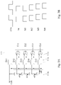
The detection system 100 includes multiple the monitors M and a processing unit 120. FIG. 1A is a schematic diagram of the detection system and the test circuits in some embodiments of the present disclosure. In some embodiments, the monitors M are arranged in the test device A10, and each of monitors M is electrically coupled to one test circuits A11 in the test device A10.
In this embodiment, the test circuits A11 can be the semiconductor elements discussed above. FIG. 1A is a schematic diagram of the relative position between the monitors M and the test circuits A11, the internal circuit and detection methods will be detailed in following paragraphs.
The processing unit 120 is electrically coupled to registers REG of the test device A10. During detecting, the test circuits A11 operates according to a test sample signal input from external device (i.e., Pattern provided by the processing unit 120), and stores the operated signal to the register REG by the monitor M. Accordingly, when the test device A10 performing various operations, the monitor M may detect the operation status and data of the corresponding test circuits A11, and transmits the detection result to the processing unit 120 by the registers REG.
FIG. 1B is a schematic diagram of the processing chip A20 to be tested in the test device A10 in some embodiments of the present disclosure. The processing chip A20 includes multiple circuits, and the processing chip A20 has multiple areas with higher temperature during operation, which are called hot spots hit spots HS. The circuit in the hot spot HS or the area adjacent to the hot spot HS is called the critical path or sub-critical path. In some embodiments, the circuit on the critical path or the sub-critical path is taken as the test circuits A11, but the present disclosure is not limited to this.
In one embodiment, the monitor M is configured to detect “the error of the time sequence” of the test circuits A11. The error of the time sequence means the relative relationship between the transmission time of a data signal and a source clock signal when the test circuits A11 transmits the data dignal according to the source clock signal. The error of the time sequence includes a setup time and a hold time. FIG. 1C is a time sequence of the signal in some embodiments of the present disclosure. The source clock signal CLK is configured to trigger the test circuits A11 operateing (e.g., input or output). The original data signal Sd is data/information that need to transmit to the test circuits A11.
As mentioned above, “the setup time” is a time length that the original data signal Sd arrives in advance before the positive edge or the negative edge of the source clock signal CLK is arrived. “The hold time” is a time length that the original data signal Sd maintains stable after the positive edge or the negative edge of the source clock signal CLK is arrived. For example, if the test circuits A11 is triggered according to the positive edge (0 to 1) or the negative edge source clock signal (1 to 0) of the source clock signal CLK level change, the setup time T1 is the time length that the original data signal is earlier than the ideal trigger time, and the hold time T2 is the time length of time the original data signal continues to maintain the same data after the ideal trigger time.
FIG. 2 is a schematic diagram of the detection system in some embodiments of the present disclosure. The detection system 100 includes a monitoring unit 110 and a processing unit 120. The monitoring unit 110 has multiple monitors M (as shown in FIG. 1A), which are electrically coupled to the test circuits A11 arranged on the different positions, so as to detect the setup times and the hold times of the corresponding test circuits A11 through the source clock signal during signal transmission.
In some embodiments, the monitoring unit 110 further includes a monitoring controller 113 and an output circuit 114, and the monitor M can be classified into a first monitoring circuit 111 and a second monitoring circuit 112 according to the detect target. The first monitoring circuit 111 is configured to detect the setup times, and the second monitoring circuit 112 is configured to detect the hold times. The monitoring controller 113 is electrically coupled to everyone of the first monitoring circuit 111 and the second monitoring circuit 112, so as to selectively detect the setup times or the hold times. The detection result of the first monitoring circuit 111 and the second monitoring circuit 112 will be transmit to the output circuit 114, and back to the processing unit 120.
FIG. 3A is a schematic diagram of the first monitoring circuit 111 corresponding to one of the test circuits A11 in some embodiments of the present disclosure. The first monitoring circuit 111 includes a first register circuit 111 a, a first delay circuit 111 b and a first logic circuit 111 c. The first register circuit 111 a is configured to receive an original data signal Sd, and output the original data signal Sd according to the source clock signal CLK. As shown in figure, in one embodiment, the first register circuit 111 a includes multiple registers D11-D15 (e.g., D type flip-flop). Registers are triggered in response to the positive edge or the negative edge of the source clock signal CLK, and are output the received original data signal Sd.
The first delay circuit 111 b is electrically coupled to the first register circuit 111 a. The first delay circuit 111 b is configured to delay the original data signal Sd. For clarity, signals, which are generated from the first delay circuit 111 b by delaying the original data signal Sd, are referred to as “the delayed data signals Sd1-Sd4”. The first delay circuit 111 b transmits the delayed data signals Sd1-Sd4 to the first register circuit 111 a, so that the first register circuit 111 a outputs the delayed data signals Sd1-Sd4 according to the source clock signal CLK.
Specifically, the first delay circuit 111 b includes multiple delay elements. The delay elements is electrically between the input terminal of the first monitoring circuit 111 and the registers D11-D15 of the first register circuit 111 a in series. Each of the delay elements is configured to delay the received signal for the same period of time (e.g., 10 picoseconds) to form the delayed data signals Sd1-Sd4. As shown in figure, the registers D11-D15 of the first register circuit 111 a receives the original data signal Sd and the delayed data signals Sd1-Sd4. Accordingly, each signal output by each of the registers D11-D15 will corresponse to the data (level) of the original data signal Sd when directly inputing to the the first monitoring circuit 111, when delaying 10 picoseconds, when delaying 20 picoseconds, when delaying 30 picoseconds, and when delaying 40 picoseconds. The numbers of registers and delay elements can be adjusted according to the test requirements, and is not limited to the one drawn in FIG. 3A.
The first logic circuit 111 c is electrically coupled to the first register circuit 111 a, and is configured to receive the original data signal Sd and the delayed data signals Sd1-Sd4 output by the first register circuit 111 a. The first logic circuit 111 c is configured to compare the difference between each of the delayed data signals Sd1-Sd4 and the original data signal Sd.
In some embodiments, the first logic circuit 111 c includes multiple XOR gates. Each of XOR gates receive the original data signal Sd and one of the delayed data signals Sd1-Sd4. The output terminal of the XOR gates is electrically to multiple output terminals E11-E14 of the first logic circuit 111 c.
When the signals of the two input terminals of the XOR gates are the same, the output signal is high level “1”. On the other hand, when the signals of the two input terminals of the XOR gates are different, the output signal is low level “0”. Accordingly, the setup time of the test circuit A11 can be obtained according to the signals output by the output terminals E11-E14. In other words, the first logic circuit 111 c compares the data of the original data signal Sd at different times before the signal edge (the positive edge or the negative edge) is delivered.
FIG. 3B is a schematic diagram of the setup time in some embodiments of the present disclosure. The signal levels output by the registers D11-D15 are “1, 1, 1, 0, 0”. The signal levels output from the first logic circuit 111 c to the output terminals E11-E14 are “1, 1, 0, 0” “. It represents the setup time of the corresponding test circuit A11 is between 20-30 picoseconds. In some other embodiments, the first logic circuit 111 c can also receive the signal output by the first register circuit 111 a through a plurality of XNOR gates.
FIG. 3C is a schematic diagram of the second monitoring circuit in some embodiments of the present disclosure. The second monitoring circuit 112 includes a second register circuit 112 a, a second delay circuit 112 b and a second logic circuit 112 c. The second register circuit 112 a is configured to receive the original data signal Sd, and output the original data signal Sd according to the source clock signal CLK. The second register circuit 112 a includes multiple registers D21-D25. For clarity, the time when the second monitoring circuit 112 receives the source clock signal CLK is referred to as the original time. The second delay circuit 112 b is electrically coupled to the second register circuit 112 a, and is configured to delay the source clock signal CLK to generate the delayed clock signals CLK1-CLK4.
Specifically, the second delay circuit 112 b includes multiple delay elements. The delay elements are electrically coupled between the input terminal of the second monitoring circuit 112 and input terminals of the registers D21-D25 of the second register circuit 112 a in series. Each of the delay elements delays the receive clock signal CLK the same period of time (e.g., 10 picoseconds) to form the delayed clock signals CLK1-CLK4. The second delay circuit 112 b transmits the delayed clock signals CLK1-CLK4 to the second register circuit 112 a, so that the second register circuit 112 a outputs the original data signal Sd to the corresponding delayed time according to the delayed clock signals CLK1-CLK4. In other words, the second register circuit 112 a sequentially outputs the original data signal Sd at the original time, at 10 picoseconds delayed, at 20 picoseconds delayed, at 30 picoseconds delayed and at 40 picoseconds delayed, respectively. The type and number of the delay elements of registers can be adjusted according to test requirements, and are not limited to those drawn in FIG. 3C.
The second logic circuit 112 c is electrically coupled to the second register circuit 112 a, and is configured to receive the original data signal Sd output by the second register circuit 112 a. Since the registers D21-D25 of the second register circuit 112 a outputs the original data signal Sd at different time according to the source clock signal CLK and the delayed clock signals CLK1-CLK4, the second logic circuit 112 c receives the signal levels of the original data signal Sd at different time, and is configured to compare the difference of the signal levels between the original data signal Sd received at the original time and at the delayed time.
In some embodiments, the second logic circuit 112 c includes multiple XOR gates. Each of the XOR gates receives the original data signal Sd output by the second register circuit 112 a. The output terminal of the XOR gates are respectively coupled to multiple output terminals E21-E24 of the second logic circuit 112 c. In other words, the second monitoring circuit 112 is configured to detect the signal level of the original data Sd when triggering by the source clock signal CLK and delayed clock signal CLK1-CLK4. Accordingly, the hold time of the test circuits A11 can be obtained by the signals output by the output terminals E21-E24.
FIG. 3D is a schematic diagram of the hold time detected by the second monitoring circuit 112 in some embodiments of the present disclosure. The signal levels output by the registers D21-D25 are “1, 1, 0, 0, 0”. The signal levels output from the second logic circuit 112 c th the output terminals E11-E14 are “1, 0, 0, 0”, it respresents that the hold time of the test circuits A11 is between 10-20 picoseconds. In some other embodiments, the first logic circuit 111 c or the second logic circuit 112 c may receive signals by multiple XNOR gates.
FIG. 3E is a schematic diagram of the first monitoring circuit 111 in some embodiments of the present disclosure. In FIG. 3E, the similar components associated with the embodiment of FIG. 3A are labeled with the same numerals for ease of understanding. The specific principle of the similar component has been explained in detail in the previous paragraphs, and unless it has a cooperative relationship with the components of FIG. 3E, it is not repeated here. In one embodiment, multiple delay elements of the first delay circuit 111 b can be implemented by inverters, and the registers D12, D14 also have inverted output terminals correspondingly. In some embodiments, the circuit implemented by inverters can be simplified.
As shown in embodiments in FIG. 3A and FIG. 3C, both of monitoring circuits 111/112 “delay” the original data signal Sd to receive the signal levels of the original data signal Sd at different time. In other embodiments, the monitoring circuit can also use the same principle to compare the signal levels of the original data signal Sd at different time by “timing boost” method. In other words, the monitoring unit 110 can adjust (e.g., delay or advance) the transmission time of the original data signal Sd to detect the setup time and the hold time of the test circuit during signal transmission.
FIG. 3F is a schematic diagram of the first monitoring circuit 111 in some embodiments of the present disclosure. FIG. 3G is a schematic diagram of the second monitoring circuit 112 in some embodiments of the present disclosure. In FIG. 3F and FIG. 3G, the similar components associated with the embodiment of FIG. 3A and FIG. 3C are labeled with the same numerals for ease of understanding. The specific principle of the similar component has been explained in detail in the previous paragraphs, and unless it has a cooperative relationship with the components of FIG. 3F and FIG. 3G, it is not repeated here.
As shown in FIG. 3F, the first monitoring circuit 111 further includes a first timing boost circuit 111 d. The first timing boost circuit 111 d is electrically coupled to the first register circuit 111 a, and is configured to transmit the original data signal Sd to the first register circuit 111 a in advance (e.g., 10 picoseconds earlier than the source clock signal). The first register circuit 111 a will also receive the original the original data signal Sd and the original data signal Sd transmitted in advance through multiple registers D11-D17, and output to the multiple output terminals E11-E16 of the first logic circuit 111 c.
Similarly, the second monitoring circuit 112 further includes a second timing boost circuit 112 d. The second timing boost circuit 112 d is electrically coupled to the second register circuit 112 a, and is configured to transmit the original data signal Sd to the second register circuit 112 a in advance (e.g., 10 picoseconds earlier than the source clock signal). The second register circuit 112 a will also receive the original the original data signal Sd and the original data signal Sd transmitted in advance through multiple registers D21-D27, and output to the multiple output terminals E21-E26 of the second logic circuit 112 c.
As shown in FIG. 2, the processing unit 120 is electrically coupled to the monitoring unit 110, so as to receive the setup time and the hold time back from the monitoring unit 110. The processing unit 120 records each of the setup time and the hold time as a detection data corresponding to one of the test circuits A11. In other words, the processing unit 120 establishes multiple detection data corresponding to the test circuits A11. As shown in FIG. 1A, each the detection data is configured to record the error value of the time sequence (i.e., the setup time, the hold time) of the same test circuits A11.
The processing unit 120 includes a data module circuit 121 and a data detection circuit 122. The data module circuit 121 selects a first part of the detection data (randomly select 5% of the detection data), as the first detection data DT1. Then, the data module circuit 121 generates regression data MR (Mathematic Regression, such as a set of mathematical polynomials) according to the first detection data DT1, and then establishes a estimation model DB. The estimation model DB is configured to estimate a signal transmission status of any one of the test circuits under different configuration conditions. The above “configuration conditions” includes the arrang position, the power supply, the logical actions during the test of the test circuits A11. The signal transmission status can include the setup time and the hold time. In other words, the estimation model DB is configured to use various configuration conditions as input parameters to estimate the error value of time sequence of the test circuits A11 during operation.
The data detection circuit 122 selects a second part of the detection data (other 95% of the detection data), as multiple second detection data DT2. The second detection data DT2 is different from the first detection data DT1 (but can be partially the same), and is configured to be compared with the estimation results generated by the estimation model DB to obtain the error value of the estimation model. In some embodiments, the estimation model DB is configured to estimate the signal transmission status of the non-critical circuit on the non-critical path of the test chip A20 (as shown in FIG. 1B).
In some embodiments, the data detection circuit 122 includes a verification circuit 122 a, and is configured to compare multiple estimation results of the estimation model DB with the second detection data DT2. For example, the verification circuit 122 a takes the configuration conditions of the second detection data DT2 as input parameters, and feed it into the estimation model DB to obtain the estimation results (e.g., an estimated setup time and an estimated the hold time). Then, the verification circuit 122 a compares the estimation results of the estimation model DB with the setup time and the hold time recorded in the second detection data to obtain the error value of the estimation model DB.
If the error value less than the threshold value (or a predetermine range), the data detection circuit 122 will generate an estimation data (estimation sample) of the test circuits according to the estimation model DB. The estimation data can be the performance of the test circuits under various conditions, and can be expressed in the form of curves, medians, averages, tables or characteristic expressions.
Therefore, by establishing the estimation model DB, the detection system 100 can obtain the estimation data of the test circuits A11 under different configuration conditions for reference, and the estimation data can be used to adjust the manufacturing process of the semiconductor elements. Since the detection system 100 establish the estimation model DB according to a part of the detection data (the first detection data), and performs verification and confirmation according to the other part of the detection data (the second detection data) after establishing the estimation model DB, the computational complexity of the processing unit 120 can be reduced under the condition of ensuring the accuracy of the model.
In some embodiments, if the error value larger than the threshold value (or the predetermine range) after obtaining the error value, such a larger than 5%, the processing unit 120 will adjust or rebuild the estimation model DB according to the detection data. The processing unit 120 selects a third part of the detection data, and adjusts the estimation model DB (e.g., the third part is different from the first detection data and the second detection data, or a part of the second detection data is added to the first detection data to form the third part).
In addition, in some embodiments, when the processing unit 120 receives the setup time and the hold time from the monitoring unit 110, the processing unit 120 also records the configuration parameters of the test circuits A11 (i.e., the corresponding control parameters of the above configuration conditions). The processing unit 120 stores the setup time corresponding to the test circuits, the hold time corresponding to the test circuits and the configuration parameters corresponding to the test circuits as the same detection data. Therefore, when verifying the error value of the estimation model DB, the configuration parameters can be used as the input parameters of the estimation model DB.
FIG. 4A is a schematic diagram of the first monitoring circuit 111, the test circuits A11 and the output circuit 114 in some embodiments of the present disclosure. In some embodiments, the output circuit 114 includes multiple shift registers RE1, RE2. Each of the shift registers RE1, RE2 corresponds to ne first monitoring circuit 111, and is configured to store the data output by the first logic circuit 111 c. The processing unit 120 determines the corresponding setup time or the corresponding hold time from the data, and stores the setup time or the hold time in multiple fields of a first monitoring table of the processing unit 120. The following is a partial embodiment of the first monitoring table:
Column 1 Column 2 Column 3 Column 4
Row 1 12 ps 30 ps  6 ps 20 ps
Row 2 10 ps  8 ps 32 ps 18 ps
As shown in above table, the fields in the first monitoring table correspond to the configuration parameters of the test circuits A11 (such as: configuration location). Furthermore, in addition to storing the setup time, the first monitoring table further stores other configuration parameters, such as IR drops, ambient temperature during detection or operations during detection. In the same way, the output circuit 114 can receive the hold time from the second monitoring circuit 112 and store it in the second monitoring table to record as the detection data.
FIG. 4B is a schematic diagram of the shift register RE1 of the output circuit 114 in some embodiments of the present disclosure. The shift registers RE1 includes multiple registers DF1-DF4 (e.g., D type flip-flop). The registers DF1-DF4 perform corresponding operations according to the source clock signal CLK and the external input trigger signal SE (e.g., the processing unit 120 receives a command, or generates according to a trigger program). FIG. 4C is a schematic diagram of one of the registers DF1-DF4 in some embodiments of the present disclosure. The signal level of the conjugate source clock signal CLKB is opposite to the source clock signal CLK, the signal SET is the execution signal in the detection system. Since one skilled in art can understand the operation of each logic element in FIG. 4B and FIG. 4C, it will not be repeated here.
FIG. 5A is a schematic diagram of the first monitoring circuit 111 in some embodiments of the present disclosure. The first logic circuit 111 c includes multiple XNOR gates. In the case that the first logic circuit 111 c is composed of the XNOR gates, the structure of the shift registers RE1 and the registers DF1-DF4 is shown in FIG. 5B and FIG. 5C. Since the operation of FIG. 5A-FIG. 5C is the same as that of the foregoing embodiment, it will not be repeated here.
FIG. 6 is a flowchart illustrating a detection method of the detection system 100 in some embodiments of the present disclosure. In step S601, the processing unit 120 transmits the control command Sc to the monitoring controller 113, so that the monitoring unit 110 detect the setup time and the hold time sequentially. The monitoring controller 113 determines the detect target according to the control command Sc.
If the detect target is “the setup time”, in step S602, the first monitoring circuit 111 of the monitoring unit 110 receives the source clock signal CLK and the original data signal Sd, and delays the original data signal Sd by the first delay circuit 111 b, so as to generate at least one delayed data signal. In this embodiment, the first delay circuit 111 b generates multiple delayed data signals Sd1-Sd4.
In step S603, the first register circuit 111 a sequentially outputs the original data signal Sd and the corresponding data (high level or low level) of the delayed data signals Sd1-Sd4 according to the source clock signal CLK. In step S604, the first logic circuit 111 c outputs the corresponding detection result according to the data output by the first register circuit 111 a. The detection result is configured to represent the setup time of the test circuits A11. As shown in FIG. 3A and above embodiments, if the detection result output by the first logic circuit 111 c is “1, 1, 0, 0”, it represents that the setup time of the test circuits A11 is between 20-30 picoseconds.
If the detect target is “the hold time”, in step S605, the second monitoring circuit 112 of the monitoring unit 110 receives the source clock signal CLK and the original data signal Sd, and delays the source clock signal CLK by the second delay circuit 112 b, so as to generate at least one delayed clock signal. In this embodiment, the second delay circuit 112 b generates multiple delayed clock signals CLK1-CLK4.
In step S606, the second register circuit 112 a sequentially output the corresponding data (high level or low level) of the original data signal Sd during different delayed time according to the source clock signal CLK and the delayed clock signals CLK1-CLK4. In step S607, the second logic circuit 112 c outputs the corresponding detection result according to the data output by the second register circuit 112. The detection result is configured to represent the hold time of the test circuits A11. As shown in FIG. 3C and above embodiments, if the detection result output by the second logic circuit 112 c is “1, 0, 0, 0”, it represents that the hold time of the test circuits A11 is bertween 10-20 picoseconds.
After obtaining the detection data of the first monitoring circuit 111 and/or the second monitoring circuit 112, in step S608, the output circuit 114 records the detection data into the first monitoring table and/or the second monitoring table, so that the processing unit 120 obtains the detection data corresponding to all of the test circuits A11.
In step S609, the data module circuit 121 of the processing unit 120 selects the first part of the detection data as the first detection data DT1, and establishes the estimation model DB according to the first detection data DT1.
In step S610, the data detection circuit 122 of the processing unit 120 selects the second part of the detection data as the second detection data DT2. In step S611, the verification circuit 122 a feeds the configuration parameters of the second detection data into the estimation model DB, so as to obtain the estimation results, and compares the estimation results with the setup time and/or the hold time of the second detection data DT2 to verify the estimation accuracy of the estimation model DB and obtains the error value.
As mentioned above, if the error value is larger than a predetermine range (or a threshold value), the detection system 100 may adjust or rebuild the estimation model DB. If the error value is within the predetermine range (or the threshold value), the processing unit 120 generates the estimation data of the test circuits according to the estimation model DB. The estimation data may the performance of the test circuits in various situations.(e.g., different configuration parameters or different paths.
The elements, method steps, or technical features in the foregoing embodiments may be combined with each other, and are not limited to the order of the specification description or the order of the drawings in the present disclosure.
It will be apparent to those skilled in the art that various modifications and variations can be made to the structure of the present disclosure without departing from the scope or spirit of the present disclosure. In view of the foregoing, it is intended that the present disclosure cover modifications and variations of this present disclosure provided they fall within the scope of the following claims.

Claims (20)

What is claimed is:
1. A setup time and hold time detection system, comprising:
a monitoring unit, electrically coupled to a plurality of test circuits, and configured to detect a plurality of setup times and a plurality of hold times of the plurality of test circuits during signal transmission according to a source clock signal; and
a processing unit, electrically coupled the monitoring unit, configured to receive the plurality of setup times and the plurality of hold times, and configured to record the plurality of setup times and the plurality of hold times as a plurality of detection data of the plurality of test circuits, wherein the processing unit comprising:
a data module circuit, configured to select a first part of the detection data as a plurality of first detection data to establish an estimation model, wherein the estimation model is configured to estimate a signal transmission status of the plurality of test circuits under different conditions; and
a data detection circuit, configured to select a second part of the detection data as a plurality of second detection data, wherein the plurality of second detection data are different from the plurality of first detection data, and are configured to compare with a plurality of estimation results generated by the estimation model to obtain an error value of the estimation model.
2. The setup time and hold time detection system of claim 1, wherein when the error value is larger than a threshold value, the processing unit is configured to select a third part of the detection data to adjust the estimation model, and the third part of the detection data is different from the first part of the detection data.
3. The setup time and hold time detection system of claim 1, wherein the monitoring unit further comprises:
a first monitoring circuit, configured to detect the plurality of setup times of the plurality of test circuits; and
a second monitoring circuit, configured to detect the plurality of hold times of the plurality of test circuits;
wherein the processing unit is configured to record a plurality of configuration parameters of the plurality of test circuits, and is configured to record the plurality of setup times of the plurality of test circuits, the plurality of hold times of the plurality of test circuits and the plurality of configuration parameters as the plurality of detection data.
4. The setup time and hold time detection system of claim 3, wherein the plurality of configuration parameters comprise a plurality of configuration positions, a plurality of IR drops or a plurality of temperatures corresponding to the plurality of test circuits.
5. The setup time and hold time detection system of claim 3, wherein the processing unit is configured to record the plurality of configuration parameters of the plurality of test circuits to a plurality of fields of a monitoring table.
6. The setup time and hold time detection system of claim 3, wherein the processing unit comprises a verification circuit, the verification circuit is configured to feed the plurality of configuration parameters into the estimation model to obtain the plurality of estimation results; and the verification circuit is further configured to compare the plurality of estimation results with the the plurality of setup times and the plurality of hold times corresponding to the plurality of configuration parameters, so as to obtain the error value.
7. The setup time and hold time detection system of claim 3, wherein the first monitoring circuit comprises:
a first register circuit, configured to receive an original data signal, and output the original data signal according to the source clock signal; and
a first delay circuit, electrically coupled to the first register circuit, wherein the first delay circuit is configured to delay the original data signal to generate a delayed data signal, and is configured to transmit the delayed data signal to the first register circuit, and the first register circuit outputs the delayed data signal according to the source clock signal.
8. The setup time and hold time detection system of claim 7, wherein the first monitoring circuit further comprises:
a first logic circuit, electrically coupled to the first register circuit to receive the original data signal and the delayed data signal, wherein the first logic circuit is configured to compare a difference between the original data signal and the delayed data signal.
9. The setup time and hold time detection system of claim 3, wherein the second monitoring circuit comprises:
a second register circuit, configured to receive an original data signal, and output the original data signal according to the source clock signal during a original time; and
a second delay circuit, electrically coupled to the second register circuit, wherein the second delay circuit is configured to delay the source clock signal to generate a delayed clock signal, and is configured to transmit the delayed clock signal to the second register circuit, and the second register circuit outputs the original data signal during a delayed time.
10. The setup time and hold time detection system of claim 9, wherein the second monitoring circuit further comprises:
a second logic circuit, electrically coupled to the second register circuit to receive the original data signal output by the second register circuit, wherein the second logic circuit is configured to compare a difference between the original data signal received at the original time and the original data signal at the delayed time.
11. A setup time and hold time detection method, comprising:
detecting, by a monitoring unit, a plurality of setup times of a plurality of test circuits and a plurality of hold times of the plurality of test circuits during signal transmission;
recording the plurality of setup times and the plurality of hold times as a plurality of detection data of the plurality of test circuits;
selecting a first part of the detection data as a plurality of first detection data, and establishing an estimation model according to the plurality of first detection data;
selecting a second part of the detection data as a plurality of second detection data, wherein the plurality of second detection data are different from the plurality of first detection data; and
comparing the plurality of second detection data with a plurality of estimation results generated by the estimation model to obtain an error value of the estimation model.
12. The setup time and hold time detection method of claim 11, further comprising:
when the error value is larger than a threshold value, selecting a third part of the detection data to adjust the estimation model, wherein the third part of the detection data is different from the first part of the detection data.
13. The setup time and hold time detection method of claim 11, further comprising:
recording a plurality of configuration parameters of the plurality of test circuits; and
recording the plurality of setup times of the plurality of test circuits, the plurality of hold times of the plurality of test circuits and the plurality of configuration parameters as the plurality of detection data.
14. The setup time and hold time detection method of claim 13, wherein the plurality of configuration parameters comprise a plurality of configuration positions, a plurality of IR drops or a plurality of temperatures corresponding to the plurality of test circuits.
15. The setup time and hold time detection method of claim 13, wherein recording the plurality of configuration parameters of the plurality of test circuits comprises:
storing the plurality of setup times and the plurality of hold times of the plurality of test circuits to a plurality of fields of a monitoring table to record the plurality of configuration parameters corresponding to the plurality of test circuits.
16. The setup time and hold time detection method of claim 13, wherein comparing the plurality of second detection data with the plurality of estimation results generated by the estimation model to obtain the error value of the estimation model comprises:
feeding, by a verification circuit, the plurality of configuration parameters into the estimation model to obtain the plurality of estimation results; and
comparing the plurality of estimation results with the the plurality of setup times and the plurality of hold times corresponding to the plurality of configuration parameters, so as to obtain the error value.
17. The setup time and hold time detection method of claim 11, wherein detecting the plurality of setup times and the plurality of hold times of the plurality of test circuits during signal transmission comprises:
receiving an original data signal by a first register circuit;
outputting the original data signal according to a source clock signal;
delaying, by a first delay circuit, the original data signal to generate a delayed data signal; and
transmitting the delayed data signal to the first register circuit, and outputting the delayed data signal according to the source clock signal by the first register circuit.
18. The setup time and hold time detection method of claim 17, wherein detecting the plurality of setup times and the plurality of hold times of the plurality of test circuits during signal transmission further comprises:
receiving the original data signal and the delayed data signal by a first logic circuit; and
comparing a difference between the original data signal and the delayed data signal.
19. The setup time and hold time detection method of claim 11, wherein detecting the plurality of setup times and the plurality of hold times of the plurality of test circuits during signal transmission comprises:
receiving an original data signal by a second register circuit;
outputting the original data signal according to the source clock signal during a original time;
delaying, by a second delay circuit, the source clock signal to generate a delayed clock signal; and
transmitting the delayed clock signal to the second register circuit, and outputting the original data signal during a delayed time by the second register circuit.
20. The setup time and hold time detection method of claim 19, wherein detecting the plurality of setup times and the plurality of hold times of the plurality of test circuits during signal transmission further comprises:
receiving, by a second logic circuit, the original data signal output by the second register circuit; and
comparing a difference between the original data signal received at the original time and the original data signal at the delayed time.
US17/448,703 2021-04-12 2021-09-23 Setup time and hold time detection system and detection method Active US11506714B2 (en)

Applications Claiming Priority (2)

Application Number Priority Date Filing Date Title
TW110113138A TW202240393A (en) 2021-04-12 2021-04-12 Setup time and hold time detection system and detection method
TW110113138 2021-04-12

Publications (2)

Publication Number Publication Date
US20220326304A1 US20220326304A1 (en) 2022-10-13
US11506714B2 true US11506714B2 (en) 2022-11-22

Family

ID=83510614

Family Applications (1)

Application Number Title Priority Date Filing Date
US17/448,703 Active US11506714B2 (en) 2021-04-12 2021-09-23 Setup time and hold time detection system and detection method

Country Status (2)

Country Link
US (1) US11506714B2 (en)
TW (1) TW202240393A (en)

Citations (12)

* Cited by examiner, † Cited by third party
Publication number Priority date Publication date Assignee Title
CN1329254A (en) 2000-06-14 2002-01-02 株式会社爱德万测试 Method and equipment for testing semiconductor device
US20110004813A1 (en) 2009-07-06 2011-01-06 Vikas Chandra Low overhead circuit and method for predicting timing errors
TW201245732A (en) 2011-05-05 2012-11-16 Novatek Microelectronics Corp Test chip and test system for integrated circuit chip using the same
US20130086444A1 (en) 2010-03-05 2013-04-04 Bao Liu Error detection code enhanced self-timed/asynchronous nanoelectronic circuits
TWI477946B (en) 2011-09-09 2015-03-21 瑞昱半導體股份有限公司 Calibration device and related method for phase difference between data and clock
TW201525497A (en) 2013-12-27 2015-07-01 Chroma Ate Inc Error compensation method and automated test equipment utilizing the method
US20170194060A1 (en) 2013-06-28 2017-07-06 SK Hynix Inc. Semiconductor device, semiconductor system including the same and test method thereof
TW201743069A (en) 2016-06-09 2017-12-16 孕龍科技股份有限公司 Logic analyzer, method of retrieving data of the same, and method of performance testing
CN107942280A (en) 2018-01-03 2018-04-20 中国电力科学研究院有限公司 A kind of method and system for being calibrated to the absolute delay time
TW201838052A (en) 2017-03-30 2018-10-16 義守大學 Defect test method and system suitable for three-dimensional wafer
CN109150175A (en) 2017-06-28 2019-01-04 美国亚德诺半导体公司 For the synchronous device and method with frequency conversion of clock
US20190033372A1 (en) 2017-07-27 2019-01-31 Teradyne, Inc. Time-aligning communication channels

Patent Citations (12)

* Cited by examiner, † Cited by third party
Publication number Priority date Publication date Assignee Title
CN1329254A (en) 2000-06-14 2002-01-02 株式会社爱德万测试 Method and equipment for testing semiconductor device
US20110004813A1 (en) 2009-07-06 2011-01-06 Vikas Chandra Low overhead circuit and method for predicting timing errors
US20130086444A1 (en) 2010-03-05 2013-04-04 Bao Liu Error detection code enhanced self-timed/asynchronous nanoelectronic circuits
TW201245732A (en) 2011-05-05 2012-11-16 Novatek Microelectronics Corp Test chip and test system for integrated circuit chip using the same
TWI477946B (en) 2011-09-09 2015-03-21 瑞昱半導體股份有限公司 Calibration device and related method for phase difference between data and clock
US20170194060A1 (en) 2013-06-28 2017-07-06 SK Hynix Inc. Semiconductor device, semiconductor system including the same and test method thereof
TW201525497A (en) 2013-12-27 2015-07-01 Chroma Ate Inc Error compensation method and automated test equipment utilizing the method
TW201743069A (en) 2016-06-09 2017-12-16 孕龍科技股份有限公司 Logic analyzer, method of retrieving data of the same, and method of performance testing
TW201838052A (en) 2017-03-30 2018-10-16 義守大學 Defect test method and system suitable for three-dimensional wafer
CN109150175A (en) 2017-06-28 2019-01-04 美国亚德诺半导体公司 For the synchronous device and method with frequency conversion of clock
US20190033372A1 (en) 2017-07-27 2019-01-31 Teradyne, Inc. Time-aligning communication channels
CN107942280A (en) 2018-01-03 2018-04-20 中国电力科学研究院有限公司 A kind of method and system for being calibrated to the absolute delay time

Also Published As

Publication number Publication date
US20220326304A1 (en) 2022-10-13
TW202240393A (en) 2022-10-16

Similar Documents

Publication Publication Date Title
US7576569B2 (en) Circuit for dynamic circuit timing synthesis and monitoring of critical paths and environmental conditions of an integrated circuit
US8843794B2 (en) Method, system and apparatus for evaluation of input/output buffer circuitry
JP4138163B2 (en) LSI test apparatus and timing calibration method thereof
US20080027662A1 (en) Method and device for estimating simultaneous switching noise in semiconductor device, and storage medium
US20090115443A1 (en) System and method for testing integrated circuit modules comprising a plurality of integrated circuit devices
US8694845B2 (en) Methods and systems for testing electronic circuits
US7777513B2 (en) Power supply voltage detection circuit and semiconductor integrated circuit device
US9998350B2 (en) Testing device and testing method
US11506714B2 (en) Setup time and hold time detection system and detection method
US20090105970A1 (en) Semiconductor tester
US20180259558A1 (en) Testing device and testing method
US7325182B2 (en) Method and circuit arrangement for testing electrical modules
US9721675B1 (en) Memory device having input circuit and operating method of same
US6966022B1 (en) System and method for determining integrated circuit logic speed
KR100898029B1 (en) Semiconductor test device and test method
US20210132147A1 (en) Test pattern generating method, test pattern generating device and fault model generating method
US11061073B2 (en) Circuit testing system and circuit testing method
US11073555B2 (en) Circuit testing system and circuit testing method
CN116974322B (en) Analyzer for capturing resistance voltage drop and analyzing method thereof
JP2016138799A (en) Semiconductor integrated circuit device and semiconductor integrated circuit device testing method
KR20090126607A (en) Semiconductor memory device
US20050114064A1 (en) Circuit for a parallel bit test of a semiconductor memory device and method thereof
US20070271057A1 (en) Inspection method of semiconductor integrated circuit and semiconductor
KR100967342B1 (en) Serial signal generator with reconfigurable memory module test device Memory module test device
CN118091359A (en) Protection circuit, method, memory and device for chip under test

Legal Events

Date Code Title Description
FEPP Fee payment procedure

Free format text: ENTITY STATUS SET TO UNDISCOUNTED (ORIGINAL EVENT CODE: BIG.); ENTITY STATUS OF PATENT OWNER: SMALL ENTITY

AS Assignment

Owner name: DIGWISE TECHNOLOGY CORPORATION, LTD, TAIWAN

Free format text: ASSIGNMENT OF ASSIGNORS INTEREST;ASSIGNORS:CHEN, SHIH-HAO;YANG, CHIH-WEN;REEL/FRAME:057614/0936

Effective date: 20210601

FEPP Fee payment procedure

Free format text: ENTITY STATUS SET TO SMALL (ORIGINAL EVENT CODE: SMAL); ENTITY STATUS OF PATENT OWNER: SMALL ENTITY

STPP Information on status: patent application and granting procedure in general

Free format text: NOTICE OF ALLOWANCE MAILED -- APPLICATION RECEIVED IN OFFICE OF PUBLICATIONS

STCF Information on status: patent grant

Free format text: PATENTED CASE

MAFP Maintenance fee payment

Free format text: PAYMENT OF MAINTENANCE FEE, 4TH YR, SMALL ENTITY (ORIGINAL EVENT CODE: M2551); ENTITY STATUS OF PATENT OWNER: SMALL ENTITY

Year of fee payment: 4