US11502190B2 - Vertical power semiconductor device, semiconductor wafer or bare-die arrangement, carrier, and method of manufacturing a vertical power semiconductor device - Google Patents
Vertical power semiconductor device, semiconductor wafer or bare-die arrangement, carrier, and method of manufacturing a vertical power semiconductor device Download PDFInfo
- Publication number
- US11502190B2 US11502190B2 US17/100,189 US202017100189A US11502190B2 US 11502190 B2 US11502190 B2 US 11502190B2 US 202017100189 A US202017100189 A US 202017100189A US 11502190 B2 US11502190 B2 US 11502190B2
- Authority
- US
- United States
- Prior art keywords
- semiconductor wafer
- carrier
- main surface
- semiconductor
- dopants
- Prior art date
- Legal status (The legal status is an assumption and is not a legal conclusion. Google has not performed a legal analysis and makes no representation as to the accuracy of the status listed.)
- Active, expires
Links
- 239000004065 semiconductor Substances 0.000 title claims abstract description 337
- 238000004519 manufacturing process Methods 0.000 title claims description 21
- 238000009792 diffusion process Methods 0.000 claims abstract description 54
- 230000007423 decrease Effects 0.000 claims abstract description 6
- 238000000034 method Methods 0.000 claims description 80
- 239000000463 material Substances 0.000 claims description 75
- 239000002019 doping agent Substances 0.000 claims description 56
- 230000008569 process Effects 0.000 claims description 18
- XUIMIQQOPSSXEZ-UHFFFAOYSA-N Silicon Chemical compound [Si] XUIMIQQOPSSXEZ-UHFFFAOYSA-N 0.000 claims description 11
- 229910052710 silicon Inorganic materials 0.000 claims description 11
- 239000010703 silicon Substances 0.000 claims description 11
- HBMJWWWQQXIZIP-UHFFFAOYSA-N silicon carbide Chemical compound [Si+]#[C-] HBMJWWWQQXIZIP-UHFFFAOYSA-N 0.000 claims description 11
- 238000001465 metallisation Methods 0.000 claims description 10
- 229910010271 silicon carbide Inorganic materials 0.000 claims description 10
- 238000005468 ion implantation Methods 0.000 claims description 8
- 230000004888 barrier function Effects 0.000 claims description 7
- 229910021420 polycrystalline silicon Inorganic materials 0.000 claims description 5
- 238000007669 thermal treatment Methods 0.000 claims description 5
- 230000000295 complement effect Effects 0.000 claims description 3
- 229910052582 BN Inorganic materials 0.000 claims description 2
- PZNSFCLAULLKQX-UHFFFAOYSA-N Boron nitride Chemical compound N#B PZNSFCLAULLKQX-UHFFFAOYSA-N 0.000 claims description 2
- 239000005380 borophosphosilicate glass Substances 0.000 claims description 2
- 239000005388 borosilicate glass Substances 0.000 claims 1
- 239000005360 phosphosilicate glass Substances 0.000 claims 1
- 235000012431 wafers Nutrition 0.000 description 149
- 239000010410 layer Substances 0.000 description 36
- BASFCYQUMIYNBI-UHFFFAOYSA-N platinum Chemical compound [Pt] BASFCYQUMIYNBI-UHFFFAOYSA-N 0.000 description 11
- 230000006870 function Effects 0.000 description 10
- 239000000758 substrate Substances 0.000 description 9
- 150000001875 compounds Chemical class 0.000 description 6
- 239000011669 selenium Substances 0.000 description 6
- BUGBHKTXTAQXES-UHFFFAOYSA-N Selenium Chemical compound [Se] BUGBHKTXTAQXES-UHFFFAOYSA-N 0.000 description 5
- 239000011521 glass Substances 0.000 description 5
- 229910052697 platinum Inorganic materials 0.000 description 5
- 229910052711 selenium Inorganic materials 0.000 description 5
- 239000000969 carrier Substances 0.000 description 4
- 238000005530 etching Methods 0.000 description 4
- 238000005259 measurement Methods 0.000 description 3
- 229910052751 metal Inorganic materials 0.000 description 3
- 239000002184 metal Substances 0.000 description 3
- 239000000126 substance Substances 0.000 description 3
- MARUHZGHZWCEQU-UHFFFAOYSA-N 5-phenyl-2h-tetrazole Chemical compound C1=CC=CC=C1C1=NNN=N1 MARUHZGHZWCEQU-UHFFFAOYSA-N 0.000 description 2
- ZOXJGFHDIHLPTG-UHFFFAOYSA-N Boron Chemical compound [B] ZOXJGFHDIHLPTG-UHFFFAOYSA-N 0.000 description 2
- 229910000530 Gallium indium arsenide Inorganic materials 0.000 description 2
- JMASRVWKEDWRBT-UHFFFAOYSA-N Gallium nitride Chemical compound [Ga]#N JMASRVWKEDWRBT-UHFFFAOYSA-N 0.000 description 2
- 229910000661 Mercury cadmium telluride Inorganic materials 0.000 description 2
- OAICVXFJPJFONN-UHFFFAOYSA-N Phosphorus Chemical compound [P] OAICVXFJPJFONN-UHFFFAOYSA-N 0.000 description 2
- 229910000577 Silicon-germanium Inorganic materials 0.000 description 2
- KXNLCSXBJCPWGL-UHFFFAOYSA-N [Ga].[As].[In] Chemical compound [Ga].[As].[In] KXNLCSXBJCPWGL-UHFFFAOYSA-N 0.000 description 2
- 230000015572 biosynthetic process Effects 0.000 description 2
- 229910052796 boron Inorganic materials 0.000 description 2
- 238000005516 engineering process Methods 0.000 description 2
- 230000005669 field effect Effects 0.000 description 2
- 239000007789 gas Substances 0.000 description 2
- 230000006872 improvement Effects 0.000 description 2
- 229910052738 indium Inorganic materials 0.000 description 2
- APFVFJFRJDLVQX-UHFFFAOYSA-N indium atom Chemical compound [In] APFVFJFRJDLVQX-UHFFFAOYSA-N 0.000 description 2
- 150000004767 nitrides Chemical class 0.000 description 2
- 239000012071 phase Substances 0.000 description 2
- 229910052698 phosphorus Inorganic materials 0.000 description 2
- 239000011574 phosphorus Substances 0.000 description 2
- 238000005001 rutherford backscattering spectroscopy Methods 0.000 description 2
- 238000000926 separation method Methods 0.000 description 2
- 239000007790 solid phase Substances 0.000 description 2
- 239000012808 vapor phase Substances 0.000 description 2
- JBRZTFJDHDCESZ-UHFFFAOYSA-N AsGa Chemical compound [As]#[Ga] JBRZTFJDHDCESZ-UHFFFAOYSA-N 0.000 description 1
- YCKRFDGAMUMZLT-UHFFFAOYSA-N Fluorine atom Chemical compound [F] YCKRFDGAMUMZLT-UHFFFAOYSA-N 0.000 description 1
- 229910002601 GaN Inorganic materials 0.000 description 1
- GYHNNYVSQQEPJS-UHFFFAOYSA-N Gallium Chemical compound [Ga] GYHNNYVSQQEPJS-UHFFFAOYSA-N 0.000 description 1
- GPXJNWSHGFTCBW-UHFFFAOYSA-N Indium phosphide Chemical compound [In]#P GPXJNWSHGFTCBW-UHFFFAOYSA-N 0.000 description 1
- NINIDFKCEFEMDL-UHFFFAOYSA-N Sulfur Chemical compound [S] NINIDFKCEFEMDL-UHFFFAOYSA-N 0.000 description 1
- 239000005864 Sulphur Substances 0.000 description 1
- LEVVHYCKPQWKOP-UHFFFAOYSA-N [Si].[Ge] Chemical compound [Si].[Ge] LEVVHYCKPQWKOP-UHFFFAOYSA-N 0.000 description 1
- 238000010521 absorption reaction Methods 0.000 description 1
- 239000000370 acceptor Substances 0.000 description 1
- 230000004913 activation Effects 0.000 description 1
- 238000001994 activation Methods 0.000 description 1
- 230000006978 adaptation Effects 0.000 description 1
- 239000012790 adhesive layer Substances 0.000 description 1
- 229910052782 aluminium Inorganic materials 0.000 description 1
- XAGFODPZIPBFFR-UHFFFAOYSA-N aluminium Chemical compound [Al] XAGFODPZIPBFFR-UHFFFAOYSA-N 0.000 description 1
- 238000004458 analytical method Methods 0.000 description 1
- 229910052787 antimony Inorganic materials 0.000 description 1
- WATWJIUSRGPENY-UHFFFAOYSA-N antimony atom Chemical compound [Sb] WATWJIUSRGPENY-UHFFFAOYSA-N 0.000 description 1
- 229910052785 arsenic Inorganic materials 0.000 description 1
- RQNWIZPPADIBDY-UHFFFAOYSA-N arsenic atom Chemical compound [As] RQNWIZPPADIBDY-UHFFFAOYSA-N 0.000 description 1
- 230000008901 benefit Effects 0.000 description 1
- 230000005540 biological transmission Effects 0.000 description 1
- 230000000903 blocking effect Effects 0.000 description 1
- 210000000746 body region Anatomy 0.000 description 1
- WZGKIRHYWDCEKP-UHFFFAOYSA-N cadmium magnesium Chemical compound [Mg].[Cd] WZGKIRHYWDCEKP-UHFFFAOYSA-N 0.000 description 1
- MCMSPRNYOJJPIZ-UHFFFAOYSA-N cadmium;mercury;tellurium Chemical compound [Cd]=[Te]=[Hg] MCMSPRNYOJJPIZ-UHFFFAOYSA-N 0.000 description 1
- 230000015556 catabolic process Effects 0.000 description 1
- 238000012512 characterization method Methods 0.000 description 1
- 230000000694 effects Effects 0.000 description 1
- 230000005684 electric field Effects 0.000 description 1
- 229910052731 fluorine Inorganic materials 0.000 description 1
- 239000011737 fluorine Substances 0.000 description 1
- 230000004927 fusion Effects 0.000 description 1
- 229910052733 gallium Inorganic materials 0.000 description 1
- HZXMRANICFIONG-UHFFFAOYSA-N gallium phosphide Chemical compound [Ga]#P HZXMRANICFIONG-UHFFFAOYSA-N 0.000 description 1
- 229910052732 germanium Inorganic materials 0.000 description 1
- GNPVGFCGXDBREM-UHFFFAOYSA-N germanium atom Chemical compound [Ge] GNPVGFCGXDBREM-UHFFFAOYSA-N 0.000 description 1
- 238000000227 grinding Methods 0.000 description 1
- 229910052739 hydrogen Inorganic materials 0.000 description 1
- 239000001257 hydrogen Substances 0.000 description 1
- 150000003949 imides Chemical class 0.000 description 1
- 239000011229 interlayer Substances 0.000 description 1
- 238000003754 machining Methods 0.000 description 1
- 229910044991 metal oxide Inorganic materials 0.000 description 1
- 150000004706 metal oxides Chemical class 0.000 description 1
- 150000002739 metals Chemical class 0.000 description 1
- 230000004048 modification Effects 0.000 description 1
- 238000012986 modification Methods 0.000 description 1
- 238000004806 packaging method and process Methods 0.000 description 1
- 238000000059 patterning Methods 0.000 description 1
- 238000005498 polishing Methods 0.000 description 1
- 238000002360 preparation method Methods 0.000 description 1
- 238000003825 pressing Methods 0.000 description 1
- 230000008707 rearrangement Effects 0.000 description 1
- 238000001004 secondary ion mass spectrometry Methods 0.000 description 1
- 230000007480 spreading Effects 0.000 description 1
- 238000003892 spreading Methods 0.000 description 1
- 238000007725 thermal activation Methods 0.000 description 1
- 230000007704 transition Effects 0.000 description 1
Images


Classifications
-
- H—ELECTRICITY
- H01—ELECTRIC ELEMENTS
- H01L—SEMICONDUCTOR DEVICES NOT COVERED BY CLASS H10
- H01L29/00—Semiconductor devices adapted for rectifying, amplifying, oscillating or switching, or capacitors or resistors with at least one potential-jump barrier or surface barrier, e.g. PN junction depletion layer or carrier concentration layer; Details of semiconductor bodies or of electrodes thereof ; Multistep manufacturing processes therefor
- H01L29/02—Semiconductor bodies ; Multistep manufacturing processes therefor
- H01L29/36—Semiconductor bodies ; Multistep manufacturing processes therefor characterised by the concentration or distribution of impurities in the bulk material
-
- H—ELECTRICITY
- H01—ELECTRIC ELEMENTS
- H01L—SEMICONDUCTOR DEVICES NOT COVERED BY CLASS H10
- H01L29/00—Semiconductor devices adapted for rectifying, amplifying, oscillating or switching, or capacitors or resistors with at least one potential-jump barrier or surface barrier, e.g. PN junction depletion layer or carrier concentration layer; Details of semiconductor bodies or of electrodes thereof ; Multistep manufacturing processes therefor
- H01L29/66—Types of semiconductor device ; Multistep manufacturing processes therefor
- H01L29/68—Types of semiconductor device ; Multistep manufacturing processes therefor controllable by only the electric current supplied, or only the electric potential applied, to an electrode which does not carry the current to be rectified, amplified or switched
- H01L29/70—Bipolar devices
- H01L29/72—Transistor-type devices, i.e. able to continuously respond to applied control signals
- H01L29/739—Transistor-type devices, i.e. able to continuously respond to applied control signals controlled by field-effect, e.g. bipolar static induction transistors [BSIT]
- H01L29/7393—Insulated gate bipolar mode transistors, i.e. IGBT; IGT; COMFET
- H01L29/7395—Vertical transistors, e.g. vertical IGBT
- H01L29/7396—Vertical transistors, e.g. vertical IGBT with a non planar surface, e.g. with a non planar gate or with a trench or recess or pillar in the surface of the emitter, base or collector region for improving current density or short circuiting the emitter and base regions
- H01L29/7397—Vertical transistors, e.g. vertical IGBT with a non planar surface, e.g. with a non planar gate or with a trench or recess or pillar in the surface of the emitter, base or collector region for improving current density or short circuiting the emitter and base regions and a gate structure lying on a slanted or vertical surface or formed in a groove, e.g. trench gate IGBT
-
- H—ELECTRICITY
- H01—ELECTRIC ELEMENTS
- H01L—SEMICONDUCTOR DEVICES NOT COVERED BY CLASS H10
- H01L29/00—Semiconductor devices adapted for rectifying, amplifying, oscillating or switching, or capacitors or resistors with at least one potential-jump barrier or surface barrier, e.g. PN junction depletion layer or carrier concentration layer; Details of semiconductor bodies or of electrodes thereof ; Multistep manufacturing processes therefor
- H01L29/66—Types of semiconductor device ; Multistep manufacturing processes therefor
- H01L29/68—Types of semiconductor device ; Multistep manufacturing processes therefor controllable by only the electric current supplied, or only the electric potential applied, to an electrode which does not carry the current to be rectified, amplified or switched
- H01L29/70—Bipolar devices
- H01L29/72—Transistor-type devices, i.e. able to continuously respond to applied control signals
- H01L29/739—Transistor-type devices, i.e. able to continuously respond to applied control signals controlled by field-effect, e.g. bipolar static induction transistors [BSIT]
- H01L29/7393—Insulated gate bipolar mode transistors, i.e. IGBT; IGT; COMFET
- H01L29/7395—Vertical transistors, e.g. vertical IGBT
-
- H—ELECTRICITY
- H01—ELECTRIC ELEMENTS
- H01L—SEMICONDUCTOR DEVICES NOT COVERED BY CLASS H10
- H01L21/00—Processes or apparatus adapted for the manufacture or treatment of semiconductor or solid state devices or of parts thereof
- H01L21/67—Apparatus specially adapted for handling semiconductor or electric solid state devices during manufacture or treatment thereof; Apparatus specially adapted for handling wafers during manufacture or treatment of semiconductor or electric solid state devices or components ; Apparatus not specifically provided for elsewhere
- H01L21/683—Apparatus specially adapted for handling semiconductor or electric solid state devices during manufacture or treatment thereof; Apparatus specially adapted for handling wafers during manufacture or treatment of semiconductor or electric solid state devices or components ; Apparatus not specifically provided for elsewhere for supporting or gripping
- H01L21/6835—Apparatus specially adapted for handling semiconductor or electric solid state devices during manufacture or treatment thereof; Apparatus specially adapted for handling wafers during manufacture or treatment of semiconductor or electric solid state devices or components ; Apparatus not specifically provided for elsewhere for supporting or gripping using temporarily an auxiliary support
-
- H—ELECTRICITY
- H01—ELECTRIC ELEMENTS
- H01L—SEMICONDUCTOR DEVICES NOT COVERED BY CLASS H10
- H01L25/00—Assemblies consisting of a plurality of individual semiconductor or other solid state devices ; Multistep manufacturing processes thereof
- H01L25/03—Assemblies consisting of a plurality of individual semiconductor or other solid state devices ; Multistep manufacturing processes thereof all the devices being of a type provided for in the same subgroup of groups H01L27/00 - H01L33/00, or in a single subclass of H10K, H10N, e.g. assemblies of rectifier diodes
- H01L25/04—Assemblies consisting of a plurality of individual semiconductor or other solid state devices ; Multistep manufacturing processes thereof all the devices being of a type provided for in the same subgroup of groups H01L27/00 - H01L33/00, or in a single subclass of H10K, H10N, e.g. assemblies of rectifier diodes the devices not having separate containers
- H01L25/065—Assemblies consisting of a plurality of individual semiconductor or other solid state devices ; Multistep manufacturing processes thereof all the devices being of a type provided for in the same subgroup of groups H01L27/00 - H01L33/00, or in a single subclass of H10K, H10N, e.g. assemblies of rectifier diodes the devices not having separate containers the devices being of a type provided for in group H01L27/00
-
- H—ELECTRICITY
- H01—ELECTRIC ELEMENTS
- H01L—SEMICONDUCTOR DEVICES NOT COVERED BY CLASS H10
- H01L27/00—Devices consisting of a plurality of semiconductor or other solid-state components formed in or on a common substrate
- H01L27/02—Devices consisting of a plurality of semiconductor or other solid-state components formed in or on a common substrate including semiconductor components specially adapted for rectifying, oscillating, amplifying or switching and having at least one potential-jump barrier or surface barrier; including integrated passive circuit elements with at least one potential-jump barrier or surface barrier
- H01L27/04—Devices consisting of a plurality of semiconductor or other solid-state components formed in or on a common substrate including semiconductor components specially adapted for rectifying, oscillating, amplifying or switching and having at least one potential-jump barrier or surface barrier; including integrated passive circuit elements with at least one potential-jump barrier or surface barrier the substrate being a semiconductor body
- H01L27/06—Devices consisting of a plurality of semiconductor or other solid-state components formed in or on a common substrate including semiconductor components specially adapted for rectifying, oscillating, amplifying or switching and having at least one potential-jump barrier or surface barrier; including integrated passive circuit elements with at least one potential-jump barrier or surface barrier the substrate being a semiconductor body including a plurality of individual components in a non-repetitive configuration
- H01L27/0611—Devices consisting of a plurality of semiconductor or other solid-state components formed in or on a common substrate including semiconductor components specially adapted for rectifying, oscillating, amplifying or switching and having at least one potential-jump barrier or surface barrier; including integrated passive circuit elements with at least one potential-jump barrier or surface barrier the substrate being a semiconductor body including a plurality of individual components in a non-repetitive configuration integrated circuits having a two-dimensional layout of components without a common active region
- H01L27/0641—Devices consisting of a plurality of semiconductor or other solid-state components formed in or on a common substrate including semiconductor components specially adapted for rectifying, oscillating, amplifying or switching and having at least one potential-jump barrier or surface barrier; including integrated passive circuit elements with at least one potential-jump barrier or surface barrier the substrate being a semiconductor body including a plurality of individual components in a non-repetitive configuration integrated circuits having a two-dimensional layout of components without a common active region without components of the field effect type
- H01L27/0647—Bipolar transistors in combination with diodes, or capacitors, or resistors, e.g. vertical bipolar transistor and bipolar lateral transistor and resistor
- H01L27/0652—Vertical bipolar transistor in combination with diodes, or capacitors, or resistors
-
- H—ELECTRICITY
- H01—ELECTRIC ELEMENTS
- H01L—SEMICONDUCTOR DEVICES NOT COVERED BY CLASS H10
- H01L29/00—Semiconductor devices adapted for rectifying, amplifying, oscillating or switching, or capacitors or resistors with at least one potential-jump barrier or surface barrier, e.g. PN junction depletion layer or carrier concentration layer; Details of semiconductor bodies or of electrodes thereof ; Multistep manufacturing processes therefor
- H01L29/02—Semiconductor bodies ; Multistep manufacturing processes therefor
- H01L29/06—Semiconductor bodies ; Multistep manufacturing processes therefor characterised by their shape; characterised by the shapes, relative sizes, or dispositions of the semiconductor regions ; characterised by the concentration or distribution of impurities within semiconductor regions
- H01L29/0603—Semiconductor bodies ; Multistep manufacturing processes therefor characterised by their shape; characterised by the shapes, relative sizes, or dispositions of the semiconductor regions ; characterised by the concentration or distribution of impurities within semiconductor regions characterised by particular constructional design considerations, e.g. for preventing surface leakage, for controlling electric field concentration or for internal isolations regions
- H01L29/0607—Semiconductor bodies ; Multistep manufacturing processes therefor characterised by their shape; characterised by the shapes, relative sizes, or dispositions of the semiconductor regions ; characterised by the concentration or distribution of impurities within semiconductor regions characterised by particular constructional design considerations, e.g. for preventing surface leakage, for controlling electric field concentration or for internal isolations regions for preventing surface leakage or controlling electric field concentration
- H01L29/0611—Semiconductor bodies ; Multistep manufacturing processes therefor characterised by their shape; characterised by the shapes, relative sizes, or dispositions of the semiconductor regions ; characterised by the concentration or distribution of impurities within semiconductor regions characterised by particular constructional design considerations, e.g. for preventing surface leakage, for controlling electric field concentration or for internal isolations regions for preventing surface leakage or controlling electric field concentration for increasing or controlling the breakdown voltage of reverse biased devices
- H01L29/0615—Semiconductor bodies ; Multistep manufacturing processes therefor characterised by their shape; characterised by the shapes, relative sizes, or dispositions of the semiconductor regions ; characterised by the concentration or distribution of impurities within semiconductor regions characterised by particular constructional design considerations, e.g. for preventing surface leakage, for controlling electric field concentration or for internal isolations regions for preventing surface leakage or controlling electric field concentration for increasing or controlling the breakdown voltage of reverse biased devices by the doping profile or the shape or the arrangement of the PN junction, or with supplementary regions, e.g. junction termination extension [JTE]
- H01L29/0619—Semiconductor bodies ; Multistep manufacturing processes therefor characterised by their shape; characterised by the shapes, relative sizes, or dispositions of the semiconductor regions ; characterised by the concentration or distribution of impurities within semiconductor regions characterised by particular constructional design considerations, e.g. for preventing surface leakage, for controlling electric field concentration or for internal isolations regions for preventing surface leakage or controlling electric field concentration for increasing or controlling the breakdown voltage of reverse biased devices by the doping profile or the shape or the arrangement of the PN junction, or with supplementary regions, e.g. junction termination extension [JTE] with a supplementary region doped oppositely to or in rectifying contact with the semiconductor containing or contacting region, e.g. guard rings with PN or Schottky junction
-
- H—ELECTRICITY
- H01—ELECTRIC ELEMENTS
- H01L—SEMICONDUCTOR DEVICES NOT COVERED BY CLASS H10
- H01L29/00—Semiconductor devices adapted for rectifying, amplifying, oscillating or switching, or capacitors or resistors with at least one potential-jump barrier or surface barrier, e.g. PN junction depletion layer or carrier concentration layer; Details of semiconductor bodies or of electrodes thereof ; Multistep manufacturing processes therefor
- H01L29/02—Semiconductor bodies ; Multistep manufacturing processes therefor
- H01L29/06—Semiconductor bodies ; Multistep manufacturing processes therefor characterised by their shape; characterised by the shapes, relative sizes, or dispositions of the semiconductor regions ; characterised by the concentration or distribution of impurities within semiconductor regions
- H01L29/0684—Semiconductor bodies ; Multistep manufacturing processes therefor characterised by their shape; characterised by the shapes, relative sizes, or dispositions of the semiconductor regions ; characterised by the concentration or distribution of impurities within semiconductor regions characterised by the shape, relative sizes or dispositions of the semiconductor regions or junctions between the regions
-
- H—ELECTRICITY
- H01—ELECTRIC ELEMENTS
- H01L—SEMICONDUCTOR DEVICES NOT COVERED BY CLASS H10
- H01L29/00—Semiconductor devices adapted for rectifying, amplifying, oscillating or switching, or capacitors or resistors with at least one potential-jump barrier or surface barrier, e.g. PN junction depletion layer or carrier concentration layer; Details of semiconductor bodies or of electrodes thereof ; Multistep manufacturing processes therefor
- H01L29/66—Types of semiconductor device ; Multistep manufacturing processes therefor
- H01L29/66007—Multistep manufacturing processes
- H01L29/66053—Multistep manufacturing processes of devices having a semiconductor body comprising crystalline silicon carbide
- H01L29/6606—Multistep manufacturing processes of devices having a semiconductor body comprising crystalline silicon carbide the devices being controllable only by variation of the electric current supplied or the electric potential applied, to one or more of the electrodes carrying the current to be rectified, amplified, oscillated or switched, e.g. two-terminal devices
-
- H—ELECTRICITY
- H01—ELECTRIC ELEMENTS
- H01L—SEMICONDUCTOR DEVICES NOT COVERED BY CLASS H10
- H01L29/00—Semiconductor devices adapted for rectifying, amplifying, oscillating or switching, or capacitors or resistors with at least one potential-jump barrier or surface barrier, e.g. PN junction depletion layer or carrier concentration layer; Details of semiconductor bodies or of electrodes thereof ; Multistep manufacturing processes therefor
- H01L29/66—Types of semiconductor device ; Multistep manufacturing processes therefor
- H01L29/66007—Multistep manufacturing processes
- H01L29/66053—Multistep manufacturing processes of devices having a semiconductor body comprising crystalline silicon carbide
- H01L29/66068—Multistep manufacturing processes of devices having a semiconductor body comprising crystalline silicon carbide the devices being controllable only by the electric current supplied or the electric potential applied, to an electrode which does not carry the current to be rectified, amplified or switched, e.g. three-terminal devices
-
- H—ELECTRICITY
- H01—ELECTRIC ELEMENTS
- H01L—SEMICONDUCTOR DEVICES NOT COVERED BY CLASS H10
- H01L29/00—Semiconductor devices adapted for rectifying, amplifying, oscillating or switching, or capacitors or resistors with at least one potential-jump barrier or surface barrier, e.g. PN junction depletion layer or carrier concentration layer; Details of semiconductor bodies or of electrodes thereof ; Multistep manufacturing processes therefor
- H01L29/66—Types of semiconductor device ; Multistep manufacturing processes therefor
- H01L29/66007—Multistep manufacturing processes
- H01L29/66075—Multistep manufacturing processes of devices having semiconductor bodies comprising group 14 or group 13/15 materials
- H01L29/66083—Multistep manufacturing processes of devices having semiconductor bodies comprising group 14 or group 13/15 materials the devices being controllable only by variation of the electric current supplied or the electric potential applied, to one or more of the electrodes carrying the current to be rectified, amplified, oscillated or switched, e.g. two-terminal devices
- H01L29/6609—Diodes
-
- H—ELECTRICITY
- H01—ELECTRIC ELEMENTS
- H01L—SEMICONDUCTOR DEVICES NOT COVERED BY CLASS H10
- H01L29/00—Semiconductor devices adapted for rectifying, amplifying, oscillating or switching, or capacitors or resistors with at least one potential-jump barrier or surface barrier, e.g. PN junction depletion layer or carrier concentration layer; Details of semiconductor bodies or of electrodes thereof ; Multistep manufacturing processes therefor
- H01L29/66—Types of semiconductor device ; Multistep manufacturing processes therefor
- H01L29/66007—Multistep manufacturing processes
- H01L29/66075—Multistep manufacturing processes of devices having semiconductor bodies comprising group 14 or group 13/15 materials
- H01L29/66227—Multistep manufacturing processes of devices having semiconductor bodies comprising group 14 or group 13/15 materials the devices being controllable only by the electric current supplied or the electric potential applied, to an electrode which does not carry the current to be rectified, amplified or switched, e.g. three-terminal devices
- H01L29/66409—Unipolar field-effect transistors
- H01L29/66477—Unipolar field-effect transistors with an insulated gate, i.e. MISFET
- H01L29/66666—Vertical transistors
-
- H—ELECTRICITY
- H01—ELECTRIC ELEMENTS
- H01L—SEMICONDUCTOR DEVICES NOT COVERED BY CLASS H10
- H01L29/00—Semiconductor devices adapted for rectifying, amplifying, oscillating or switching, or capacitors or resistors with at least one potential-jump barrier or surface barrier, e.g. PN junction depletion layer or carrier concentration layer; Details of semiconductor bodies or of electrodes thereof ; Multistep manufacturing processes therefor
- H01L29/66—Types of semiconductor device ; Multistep manufacturing processes therefor
- H01L29/68—Types of semiconductor device ; Multistep manufacturing processes therefor controllable by only the electric current supplied, or only the electric potential applied, to an electrode which does not carry the current to be rectified, amplified or switched
- H01L29/76—Unipolar devices, e.g. field effect transistors
- H01L29/772—Field effect transistors
- H01L29/78—Field effect transistors with field effect produced by an insulated gate
- H01L29/7827—Vertical transistors
-
- H—ELECTRICITY
- H01—ELECTRIC ELEMENTS
- H01L—SEMICONDUCTOR DEVICES NOT COVERED BY CLASS H10
- H01L29/00—Semiconductor devices adapted for rectifying, amplifying, oscillating or switching, or capacitors or resistors with at least one potential-jump barrier or surface barrier, e.g. PN junction depletion layer or carrier concentration layer; Details of semiconductor bodies or of electrodes thereof ; Multistep manufacturing processes therefor
- H01L29/66—Types of semiconductor device ; Multistep manufacturing processes therefor
- H01L29/86—Types of semiconductor device ; Multistep manufacturing processes therefor controllable only by variation of the electric current supplied, or only the electric potential applied, to one or more of the electrodes carrying the current to be rectified, amplified, oscillated or switched
- H01L29/861—Diodes
- H01L29/8613—Mesa PN junction diodes
-
- H—ELECTRICITY
- H01—ELECTRIC ELEMENTS
- H01L—SEMICONDUCTOR DEVICES NOT COVERED BY CLASS H10
- H01L2221/00—Processes or apparatus adapted for the manufacture or treatment of semiconductor or solid state devices or of parts thereof covered by H01L21/00
- H01L2221/67—Apparatus for handling semiconductor or electric solid state devices during manufacture or treatment thereof; Apparatus for handling wafers during manufacture or treatment of semiconductor or electric solid state devices or components; Apparatus not specifically provided for elsewhere
- H01L2221/683—Apparatus for handling semiconductor or electric solid state devices during manufacture or treatment thereof; Apparatus for handling wafers during manufacture or treatment of semiconductor or electric solid state devices or components; Apparatus not specifically provided for elsewhere for supporting or gripping
- H01L2221/68304—Apparatus for handling semiconductor or electric solid state devices during manufacture or treatment thereof; Apparatus for handling wafers during manufacture or treatment of semiconductor or electric solid state devices or components; Apparatus not specifically provided for elsewhere for supporting or gripping using temporarily an auxiliary support
- H01L2221/68318—Auxiliary support including means facilitating the separation of a device or wafer from the auxiliary support
-
- H—ELECTRICITY
- H01—ELECTRIC ELEMENTS
- H01L—SEMICONDUCTOR DEVICES NOT COVERED BY CLASS H10
- H01L2221/00—Processes or apparatus adapted for the manufacture or treatment of semiconductor or solid state devices or of parts thereof covered by H01L21/00
- H01L2221/67—Apparatus for handling semiconductor or electric solid state devices during manufacture or treatment thereof; Apparatus for handling wafers during manufacture or treatment of semiconductor or electric solid state devices or components; Apparatus not specifically provided for elsewhere
- H01L2221/683—Apparatus for handling semiconductor or electric solid state devices during manufacture or treatment thereof; Apparatus for handling wafers during manufacture or treatment of semiconductor or electric solid state devices or components; Apparatus not specifically provided for elsewhere for supporting or gripping
- H01L2221/68304—Apparatus for handling semiconductor or electric solid state devices during manufacture or treatment thereof; Apparatus for handling wafers during manufacture or treatment of semiconductor or electric solid state devices or components; Apparatus not specifically provided for elsewhere for supporting or gripping using temporarily an auxiliary support
- H01L2221/68327—Apparatus for handling semiconductor or electric solid state devices during manufacture or treatment thereof; Apparatus for handling wafers during manufacture or treatment of semiconductor or electric solid state devices or components; Apparatus not specifically provided for elsewhere for supporting or gripping using temporarily an auxiliary support used during dicing or grinding
-
- H—ELECTRICITY
- H01—ELECTRIC ELEMENTS
- H01L—SEMICONDUCTOR DEVICES NOT COVERED BY CLASS H10
- H01L2221/00—Processes or apparatus adapted for the manufacture or treatment of semiconductor or solid state devices or of parts thereof covered by H01L21/00
- H01L2221/67—Apparatus for handling semiconductor or electric solid state devices during manufacture or treatment thereof; Apparatus for handling wafers during manufacture or treatment of semiconductor or electric solid state devices or components; Apparatus not specifically provided for elsewhere
- H01L2221/683—Apparatus for handling semiconductor or electric solid state devices during manufacture or treatment thereof; Apparatus for handling wafers during manufacture or treatment of semiconductor or electric solid state devices or components; Apparatus not specifically provided for elsewhere for supporting or gripping
- H01L2221/68304—Apparatus for handling semiconductor or electric solid state devices during manufacture or treatment thereof; Apparatus for handling wafers during manufacture or treatment of semiconductor or electric solid state devices or components; Apparatus not specifically provided for elsewhere for supporting or gripping using temporarily an auxiliary support
- H01L2221/6834—Apparatus for handling semiconductor or electric solid state devices during manufacture or treatment thereof; Apparatus for handling wafers during manufacture or treatment of semiconductor or electric solid state devices or components; Apparatus not specifically provided for elsewhere for supporting or gripping using temporarily an auxiliary support used to protect an active side of a device or wafer
-
- H—ELECTRICITY
- H01—ELECTRIC ELEMENTS
- H01L—SEMICONDUCTOR DEVICES NOT COVERED BY CLASS H10
- H01L29/00—Semiconductor devices adapted for rectifying, amplifying, oscillating or switching, or capacitors or resistors with at least one potential-jump barrier or surface barrier, e.g. PN junction depletion layer or carrier concentration layer; Details of semiconductor bodies or of electrodes thereof ; Multistep manufacturing processes therefor
- H01L29/02—Semiconductor bodies ; Multistep manufacturing processes therefor
- H01L29/12—Semiconductor bodies ; Multistep manufacturing processes therefor characterised by the materials of which they are formed
- H01L29/16—Semiconductor bodies ; Multistep manufacturing processes therefor characterised by the materials of which they are formed including, apart from doping materials or other impurities, only elements of Group IV of the Periodic System
- H01L29/167—Semiconductor bodies ; Multistep manufacturing processes therefor characterised by the materials of which they are formed including, apart from doping materials or other impurities, only elements of Group IV of the Periodic System further characterised by the doping material
Definitions
- the present disclosure is related to semiconductor devices, in particular to vertical power semiconductor devices, a semiconductor wafer or a bare-die arrangement, a carrier, and methods of manufacturing a vertical power semiconductor device.
- Semiconductor wafers are typically available in standard wafer sizes and/or thicknesses.
- standard wafer diameters are 2 inch (50 mm), 4 inch (100 mm), 6 inch (150 mm), inch (200 mm) or 12 inch (300 mm).
- a standard wafer thickness may be, for example, 725 ⁇ m.
- Attempts have been made to reduce the final thickness of semiconductor material to improve device characteristics.
- a thinner semiconductor die may result in lower on-state resistance.
- the thermal budget applied to the thin wafers may complicate the handling and processing of semiconductor wafers that are thinner than standard wafers.
- an auxiliary carrier may be reversibly bonded to a semiconductor wafer to increase mechanical stability but may also cause additional challenges in process technology.
- a vertical power semiconductor device includes a semiconductor body having a first main surface and a second main surface opposite to the first main surface.
- a thickness of the semiconductor body between the first main surface and the second main surface ranges from 40 ⁇ m to 200 ⁇ m.
- Active device elements are formed in the semiconductor body at the first main surface.
- Edge termination elements at least partly surround the active device elements at the first main surface.
- a diffusion region extends into the semiconductor body from the second main surface.
- a doping concentration profile of the diffusion region decreases from a peak concentration Ns at the second main surface to a concentration Ns/e, e being Euler's number, over a vertical distance ranging from 1 ⁇ m to 5 ⁇ m.
- the semiconductor wafer or the bare-die arrangement includes a plurality of semiconductor dies, wherein each or some of the plurality of semiconductor dies includes the vertical power semiconductor device as defined above.
- the carrier includes a carrier body.
- the carrier further includes a bonding material on a first main surface of the carrier body.
- the carrier is configured to be attached to a semiconductor wafer by wafer bonding via the bonding material.
- Dopants are integrated in a part of the carrier at the first main surface.
- the dopants are configured to exit, e.g. out diffuse the carrier by thermal processing, and are configured to form n-type or p-type doping in the semiconductor wafer.
- the method includes forming active device elements in a semiconductor wafer at a first main surface of the semiconductor wafer.
- the method further includes forming edge termination elements at least partly surrounding the active device elements at the first main surface.
- the method further includes reducing a thickness of the semiconductor wafer at a second side opposite to the first main surface.
- the method further includes bonding the semiconductor wafer to a carrier via the second side.
- the method further includes introducing dopants from the carrier into the semiconductor wafer through a second main surface of the semiconductor wafer at the second side.
- the method includes forming active device elements in a semiconductor wafer at a first main surface of the semiconductor wafer.
- the method further includes forming edge termination elements at least partly surrounding the active device elements at the first main surface.
- the method further includes reducing a thickness of the semiconductor wafer at a second side opposite to the first main surface.
- the method further includes bonding the semiconductor wafer to a carrier via the second side.
- the method further includes introducing dopants into the semiconductor wafer through a second main surface of the semiconductor wafer at the second side prior to bonding the semiconductor wafer to a carrier via the second side.
- An example of the present disclosure relates to another method of manufacturing a vertical power semiconductor device.
- the method includes forming active device elements in a semiconductor wafer at a first main surface of the semiconductor wafer. Thereafter, the method further includes reducing a thickness of the semiconductor wafer at a second side opposite to the first main surface. Thereafter, the method further includes bonding the semiconductor wafer to a carrier via the second side. Thereafter, the method further includes subjecting the wafer to a thermal treatment of at least 600° C.
- An example of the present disclosure relates to another method of manufacturing a vertical power semiconductor device.
- the method includes forming active device elements in a semiconductor wafer at a first main surface of the semiconductor wafer.
- the method further includes reducing a thickness of the semiconductor wafer at a second side opposite to the first main surface.
- the method further includes bonding the semiconductor wafer to a carrier via the second side.
- the method further includes applying a metallization layer on the first main surface prior to removing the carrier.
- FIG. 1 is a schematic cross-sectional view for illustrating an example of a power semiconductor device.
- FIGS. 2A to 6B are schematic top views and cross-sectional views for illustrating examples of carriers.
- FIGS. 7A to 9 are schematic cross-sectional views for illustrating methods for manufacturing a power semiconductor device.
- electrically connected describes a permanent low-resistive connection between electrically connected elements, for example a direct contact between the concerned elements or a low-resistive connection via a metal and/or heavily doped semiconductor material.
- electrically coupled includes that one or more intervening element(s) adapted for signal and/or power transmission may be connected between the electrically coupled elements, for example, elements that are controllable to temporarily provide a low-resistive connection in a first state and a high-resistive electric decoupling in a second state.
- An ohmic contact is a non-rectifying electrical junction with a linear or almost linear current-voltage characteristic.
- Ranges given for physical dimensions include the boundary values. For example, a range for a parameter y from a to b reads as a ⁇ y ⁇ b. The same holds for ranges with one boundary value like “at most” and “at least”.
- a further component e.g., a further layer may be positioned between the two elements (e.g., a further layer may be positioned between a layer and a substrate if the layer is “on” said substrate).
- An example of a vertical power semiconductor device may include a semiconductor body having a first main surface and a second main surface opposite to the first main surface. A thickness of the semiconductor body between the first main surface and the second main surface may range from 40 ⁇ m to 200 ⁇ m.
- the vertical power semiconductor device may further comprise active device elements in the semiconductor body at the first main surface.
- the vertical power semiconductor device may further comprise edge termination elements at least partly surrounding the active device elements at the first main surface.
- the vertical power semiconductor device may further comprise a diffusion region extending into the semiconductor body from the second main surface. A doping concentration profile of the diffusion region may decrease from a peak concentration Ns at the second main surface to a concentration Ns/e, e being Euler's number, over a vertical distance ranging from 1 ⁇ m to 5 ⁇ m.
- the vertical power semiconductor device may be a power semiconductor diode, or a power semiconductor IGBT (insulated gate bipolar transistor), or a power semiconductor transistor such as a power semiconductor IGFET (insulated gate field effect transistor, e.g. a metal oxide semiconductor field effect transistor).
- the vertical power semiconductor device may be configured to conduct currents of more than 1 A or more than 10 A or even more than 30 A and may be further configured to block voltages between load terminals, e.g. between drain and source of a MOSFET, or between emitter and collector of an IGBT, or between cathode and anode of a diode, in the range of several hundreds of up to several thousands of volts, e.g.
- the blocking voltage may correspond to a voltage class specified in a datasheet of the power semiconductor device, for example.
- the semiconductor body may include or consist of a semiconductor material from the group IV elemental semiconductors, IV-IV compound semiconductor material, III-V compound semiconductor material, or II-VI compound semiconductor material.
- semiconductor materials from the group IV elemental semiconductors include, inter alia, silicon (Si) and germanium (Ge).
- Examples of IV-IV compound semiconductor materials include, inter alia, silicon carbide (SiC) and silicon germanium (SiGe).
- III-V compound semiconductor material examples include, inter alia, gallium arsenide (GaAs), gallium nitride (GaN), gallium phosphide (GaP), indium phosphide (InP), indium gallium nitride (InGaN) and indium gallium arsenide (InGaAs).
- II-VI compound semiconductor materials include, inter alia, cadmium telluride (CdTe), mercury-cadmium-telluride (CdHgTe), and cadmium magnesium telluride (CdMgTe).
- the semiconductor body may be a magnetic Czochralski (MCZ) or a float zone (FZ) silicon semiconductor body.
- the active device elements may be formed in an active device area of the semiconductor body at the first main surface.
- the active device area is an area of the semiconductor body where a load current flow enters/exits the semiconductor body through the first main surface.
- the active device area may include source regions electrically connected to a contact electrode through the first main surface.
- a source to drain current or emitter to collector current may flow from the contact electrode through the first main surface into the source regions.
- the active device area may include anode or cathode regions electrically connected to the contact electrode through the first main surface.
- An anode to cathode current may flow from the contact electrode through the first main surface into the anode or cathode regions.
- the active device area may be restricted to a first part of the first main surface through which load current flow is guided, for example.
- the edge termination elements may be formed in an edge termination area, which is an area of the semiconductor body that partly or fully surrounds the active device area. Since pn junctions within the semiconductor body, e.g. pn junctions between a body region and a drift zone of an IGFET or an IGBT or pn junctions between a cathode and an anode region of a diode, are not infinite, but terminate at the edge zones of the semiconductor body, this edge effect limits the device breakdown voltage below the ideal value that is set by the infinite parallel plane junction. Care must be taken to ensure proper and efficient termination of the pn junction at the edge of the semiconductor body.
- the edge termination area is a measure for ensuring proper and efficient termination of the pn junction.
- the edge termination structures are formed for lowering the electric field at the edge of the semiconductor body.
- a lateral dimension of the edge termination area may vary.
- Semiconductor devices with higher voltage classes typically require larger lateral extensions of their edge termination areas for ensuring proper termination of the pn junction.
- edge termination structures in the edge termination area include field plates, junction termination extension (JTE) structures, variation of lateral doping (VLD) structures, for example.
- the edge termination area may be restricted to a second part of the first main surface i) that fully or partly surrounds the first part of the active device area, and ii) through which no load current flow is guided through the first main surface to the contact electrode, and iii) that contributes to the termination of the pn junction.
- the diffusion region extending into the semiconductor body from the second main surface may include dopants introduced into the semiconductor body by a vapor phase diffusion source and/or by a solid phase diffusion source.
- a Gaussian function or complementary error function may fit to the doping concentration profile of the diffusion region.
- the doping concentration profile may be determined by any appropriate characterization method, e.g. by Secondary Ion Mass Spectrometry (SIMS) for direct measurements of atom concentrations, and/or by Rutherford Backscattering (RBS) for direct measurements of atom concentrations, and/or by various methods for measuring the conductivity as a function of depth for semiconductors, which corresponds more or less directly to the concentration of doping atoms.
- SIMS Secondary Ion Mass Spectrometry
- RBS Rutherford Backscattering
- capacity as a function of the applied voltage for MOS and junction structures, spreading resistance measurements, or microwave absorption may be used to determine the doping concentration profile of the diffusion region.
- Fitting the Gaussian function or error function to the experimental values of the doping concentration profile of the diffusion region may be carried out by model fitting of experimental results.
- model fitting is by the minimization of the least squares.
- the analysis of experimental results may also be carried out by fitting the models' equations of the physics models, e.g. Fick's laws, to the experimental results in order to obtain the physical parameters relevant for the diffusion region.
- the diffusion region may be a rear side emitter region of a power insulated gate bipolar transistor, or an anode or cathode contact region of a power semiconductor diode.
- Another example of the present disclosure relates to a semiconductor wafer or a bare-die arrangement comprising a plurality of semiconductor dies.
- Each or some of the plurality of semiconductor dies comprises the vertical power semiconductor device according to any of the examples above or below.
- a diameter of the semiconductor wafer is equal to 200 mm or larger.
- the carrier may comprise a carrier body.
- the carrier may further comprise a bonding material on a first main surface of the carrier body, wherein the carrier is configured to be attached to a semiconductor wafer by wafer bonding via the bonding material.
- the carrier may further comprise dopants integrated in a first part, e.g. surface part of the carrier at the first main surface.
- the dopants are configured to exit the carrier by thermal processing, and are configured to form n-type or p-type doping in the semiconductor wafer.
- the carrier may comprise a second part that is free of the dopants.
- the second part of the carrier adjoins a second main surface of the carrier opposite to the first main surface.
- an area at the first surface where the dopants are integrated in the carrier may be larger than 70%, or larger than 80%, or larger than 90% of a total area of the first main surface, for example.
- more than 70%, or more than 80% or more than 90% of the first surface is configured as a dopant source, for example.
- the dopants may exit the carrier by out-diffusion caused by the thermal processing.
- boron (B), aluminum (Al), gallium (Ga), indium (In) or any combination thereof may be used for p-type doping in the silicon semiconductor wafer.
- phosphorus (P), arsenic (As), antimony (Sb), selenium (Se) or Sulphur (S) or any combination thereof may be used for n-type doping in the silicon semiconductor wafer.
- the carrier may be disc-shaped having a diameter equal to 200 mm or larger.
- the carrier body may include one or more of silicon, borophosphosilicate (BPSG) glass, borosilicate (BSG) glass, phosphosilicate (PSG) glass, boron nitride, doped or undoped polycrystalline silicon, silicon carbide.
- BPSG borophosphosilicate
- BSG borosilicate
- PSG phosphosilicate
- the dopants may be included in the bonding material of the carrier.
- exemplary materials for the bonding material include any or any combination of, oxides of silicon, nitrides of silicon, metals, polycrystalline silicon.
- polycrystalline silicon may be used as bonding material, for example.
- the dopants may be included in a semiconductor region of the carrier body at the first main surface.
- the carrier may be a semiconductor carrier including the dopants in a region at the first main surface.
- the carrier may be formed by a material different from semiconductor material, e.g. glass or any other material that has a coefficient of thermal expansion that is adapted to the material of the semiconductor wafer for bonding.
- the dopants may be introduced into the carrier by an ion implantation step and/or a diffusion step.
- an arrangement of the bonding material on the first main surface of the carrier body includes one or more of a ring or ring segments along a circumference of the carrier body, a pattern of regularly arranged islands, a plurality of stripes arranged in parallel.
- the carrier may further comprise a semiconductor layer over the carrier body.
- the dopants may be included in the semiconductor layer, and the bonding material may be arranged on the semiconductor layer.
- the carrier may further comprise a diffusion barrier arranged between the semiconductor layer and the carrier body.
- the diffusion barrier may hinder the dopants from diffusing through the carrier which may be undesired, e.g. because the dopants may then not be available for doping of a semiconductor wafer.
- a diffusion barrier made of or including SiC may be used for platinum (Pt) doping, e.g. during a life-time killing adjustment of a high power diode, for example.
- the method may comprise forming active device elements in a semiconductor wafer at a first main surface of the semiconductor wafer.
- the method may further comprise forming edge termination elements at least partly surrounding the active device elements at the first main surface.
- the method may further comprise reducing a thickness of the semiconductor wafer at a second side opposite to the first main surface. After the step of reducing the thickness, the method may further comprise bonding the semiconductor wafer to a carrier via the second side.
- the method may further comprise introducing dopants from the carrier into the semiconductor wafer through a second main surface of the semiconductor wafer at the second side.
- the carrier and the semiconductor substrate may be connected by direct bonding or by reactive bonding.
- Adhesion between directly bonded layers and substrates may be based on chemical bonds, hydrogen bonds, metallic bonds, ionic bonds and/or covalent bonds, for example.
- Direct bonding may include exerting a physical force pressing the semiconductor substrate and the handle substrate against each other, a thermal treatment of at least one of the bonded surfaces at moderate temperature or a combination of both (fusion bonding, thermo-compressive bonding, bonding by atomic rearrangement).
- Direct bonding may include the absence of any additional intermediate layer, for example, of an adhesive layer.
- An adhesion layer e.g. a nitride layer, may be arranged at the interface where the handle substrate and the semiconductor substrate are attached to one another, for example.
- the dopants may exit the carrier, e.g. by a thermal out-diffusion process, and enter the semiconductor wafer by diffusion in a state where the carrier is bonded to the semiconductor wafer.
- the carrier not only functions as a mechanical support for the thinned semiconductor wafer, but also, e.g. at the same time, functions as a doping source for introducing dopants into the semiconductor wafer, e.g. for forming any kind of doped regions at a rear side of the semiconductor wafer such as emitter regions of power IGBTs or power diodes or field stop zones.
- This may allow for increasing depth, electrically active doping dose and homogeneity of rear side emitters and/or field stop zones of power semiconductor devices, for example.
- improved electric characteristics of power semiconductor devices may be achieved, e.g. improved short-circuit robustness and/or improved overcurrent turn-off capability.
- the thickness of the semiconductor wafer may be reduced by removing material of the semiconductor wafer from the second side of the semiconductor wafer.
- the material may be removed by any material removal technique, e.g. abrasive machining processes such as grinding, chemical material removal such as e.g. etching, or chemical mechanical polishing (CMP).
- abrasive machining processes such as grinding
- chemical material removal such as e.g. etching
- CMP chemical mechanical polishing
- Patterning of masks, e.g. resist masks or hard masks may allow for excluding certain areas of the wafer from material removal, e.g. a ring at a circumference of the semiconductor wafer.
- the thickness of the semiconductor wafer may be reduced by separating the wafer in a first part and a second part by a wafer split process, e.g. by a so-called cold-split and/or smart cut process.
- the vertical power semiconductor device may be a vertical power semiconductor device as described above or below, and the diffusion region may be formed by introducing the dopants from the carrier into the semiconductor wafer.
- the carrier may be a carrier as described in any of the examples above or below.
- the method may further comprise separating the semiconductor wafer from the carrier by at least one etch process removing at least part of a bonding material.
- an etch solution may weaken a bond between the semiconductor wafer and the carrier by removing the bonding material from an outer circumference of a bonding interface toward a center of the bonding interface, for example.
- the bonding material on the carrier may be formed in such an arrangement or shape that allows an etch solution to be guided toward a center of the carrier.
- channels may be formed at a bonding interface between the semiconductor carrier and the carrier.
- Exemplary arrangements of the bonding material on the carrier may include, inter alia, separate islands and parallel stripes.
- the thickness of the semiconductor wafer may be reduced in a central region of the semiconductor wafer, thereby maintaining a thickness of a ring or ring segments of the semiconductor wafer at a circumference of the semiconductor wafer.
- the ring or ring segments may contribute to mechanical stability of the thinned semiconductor wafer, for example.
- the method may further comprise attaching a mechanical support element on the first main surface of the semiconductor wafer.
- the method may comprise forming active device elements in a semiconductor wafer at a first main surface of the semiconductor wafer.
- the method may further comprise forming edge termination elements at least partly surrounding the active device elements at the first main surface.
- the method may further comprise reducing a thickness of the semiconductor wafer at a second side opposite to the first main surface.
- the method may further comprise bonding the semiconductor wafer to a carrier via the second side, e.g. after the process of reducing the thickness of the semiconductor wafer at the second side.
- the method may further comprise introducing dopants into the semiconductor wafer through a second main surface of the semiconductor wafer at the second side prior to bonding the semiconductor wafer to a carrier via the second side.
- the method may further comprise subjecting the wafer to a thermal treatment of at least 600° C.
- the dopants may be introduced into the second main surface of the semiconductor wafer by ion implantation.
- the method may comprise forming active device elements in a semiconductor wafer at a first main surface of the semiconductor wafer. Thereafter, the method may further comprise reducing a thickness of the semiconductor wafer at a second side opposite to the first main surface. Thereafter, the method may further comprise bonding the semiconductor wafer to a carrier via the second side. Thereafter, the method may further comprise subjecting the wafer to a thermal treatment of at least 600° C.
- the method may comprise forming active device elements in a semiconductor wafer at a first main surface of the semiconductor wafer.
- the method may further comprise reducing a thickness of the semiconductor wafer at a second side opposite to the first main surface.
- the method may further comprise bonding the semiconductor wafer to a carrier via the second side.
- a metallization layer may be applied on the first main surface prior to removing the carrier.
- at least one metallization layer and optional interlayer dielectric layers as well as imide layer(s) may be applied, for example.
- a diameter of the semiconductor wafer may be equal to 200 mm or larger.
- FIG. 1 is a schematic cross-sectional view illustrating an embodiment of a vertical power semiconductor device 100 .
- the vertical power semiconductor device 100 includes a semiconductor body 102 having a first main surface 104 and a second main surface 106 opposite to the first main surface 104 .
- a thickness d of the semiconductor body 102 between the first main surface 104 and the second main surface 106 ranges from 40 ⁇ m to 200 ⁇ m.
- Active device elements 108 are formed in the semiconductor body 102 at the first main surface 104 .
- the active device elements 108 are illustrated in a simplified manner by a dashed box defining a portion of the semiconductor body 102 , e.g. an active area, where the active device elements 108 are located.
- the active device elements may comprise n- and/or p-doped semiconductor regions of specific doping and arrangement, for example.
- Edge termination elements 110 at least partly surround the active device elements 108 at the first main surface 104 .
- the edge termination elements 110 are illustrated in a simplified manner by dashed boxes defining a portion of the semiconductor body, e.g. an edge termination area, where the edge termination elements 110 are located.
- Examples of the edge termination elements 110 are field plates, junction termination extension (JTE) structures, variation of lateral doping (VLD) structures, for example.
- a diffusion region 112 extends into the semiconductor body 102 from the second main surface 106 .
- a doping concentration profile c of the diffusion region 112 versus a vertical direction y is schematically illustrated in a graph below the cross-section.
- the doping concentration profile c decreases from a peak concentration Ns at the second main surface 106 to a concentration Ns/e, e being Euler's number, over a vertical distance ⁇ y ranging from 1 ⁇ m to 5 ⁇ m, or from 2 ⁇ m to 5 ⁇ m.
- the doping concentration profile c of the diffusion region 112 differs from typical rear side diffusion profiles manufactured by laser activation of ultra-shallow junctions with respect to profile shape and profile depth, for example. Since the diffusion region 112 may include dopants introduced into the semiconductor body 102 by a vapor phase diffusion source and/or by a solid phase diffusion source, a Gaussian function or complementary error function may fit to the doping concentration profile of the diffusion region 112 . Since a wiring area above the first main surface 104 is not yet formed when introducing the dopants via the second main surface 106 for forming the diffusion region 112 , high temperature processes, e.g. thermal processing above 600° C., may be applied for forming the diffusion region 112 .
- high temperature processes e.g. thermal processing above 600° C.
- a desired doping profile and depth may be achieved compared with process technologies that are limited in thermal budget due to front side metallization layer(s) that is (are) already present when the thinned semiconductor wafers are processed at the second main surface 106 , for example.
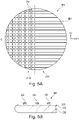
- FIGS. 2A to 6B are schematic top views and schematic cross-sectional views for illustrating examples of carriers 200 .
- Each of the carriers 200 includes a carrier body 202 and a bonding material 204 on a first main surface 208 of the carrier body 202 .
- the carrier 200 is configured to be attached to a semiconductor wafer by wafer bonding via the bonding material 204 .
- Exemplary structural and functional details of the carrier body and the bonding material as described with reference to the examples above likewise apply to the examples illustrated in the figures.
- Dopants may be integrated in the bonding material 204 of the carrier 200 and/or in a semiconductor region of the carrier body 202 at the first main surface 208 of the carrier 200 .
- the bonding material 204 is arranged along an edge of the carrier body 202 .
- the bonding material 204 may be shaped as a ring on a semiconductor wafer extending along a circumference of the semiconductor wafer.
- the dopants may be integrated in a semiconductor region 210 of the carrier body 202 at the first main surface 208 .
- the dopants may be introduced into the carrier body 202 by one or more ion implantation processes and/or diffusion processes, for example.
- the bonding material 204 is also arranged along the edge of the carrier body 202 similar to the example of FIGS. 2A , 2 B.
- the bonding material 204 is arranged as a sequence of ring segments 2041 separated from one another by channels 212 .
- Dimensions of the channels 212 may be equal or may differ from one another.
- dimensions of the ring segments 2041 of the bonding material 204 may be equal or may differ from one another.
- Dimensions and arrangement of the ring segments 2041 and the channels 212 may be adjusted for achieving desired bonding properties and separation or detachment properties between the carrier 200 and a semiconductor wafer.
- an etch solution may flow through the channels 212 for etching the bonding material 204 when separating the carrier 202 and from a semiconductor wafer.
- the bonding material 204 is also arranged along an edge of the carrier body 202 similar to the example of FIGS. 2A, 2B .
- the bonding material 204 is further arranged in the shape of parallel stripes extending along a first lateral direction x 1 and further extending along a second lateral direction x 2 .
- Areas 214 that are laterally confined by the stripe-shaped bonding material 204 may correspond to die areas of the semiconductor wafer, for example.
- the stripe-shaped bonding material 204 may be arranged in a kerf area of the semiconductor wafer, for example.
- the kerf area is an area that is removed when separating the semiconductor wafer into separate chips or dies by a dicing process, for example.
- the bonding material 204 in the example of FIGS. 4A, 4B may also be in the shape of ring segments 2041 with channels 212 between neighboring ring segments 2041 , for example.
- the bonding material 204 is arranged in the shape of parallel stripes extending along a first lateral direction x 1 and further extending along a second lateral direction x 2 .
- the bonding material 204 is arranged as parallel stripes extending in only one of the first lateral direction x 1 and the second lateral direction x 2 .
- the bonding material 204 is arranged as parallel stripes extending along both of the first lateral direction x 1 and the second lateral direction x 2 .
- the bonding material 204 may be arranged in the shape of a grid in some areas of the carrier 200 , e.g. the second area 2142 , and may be arranged in the shape of parallel stripes extending along one lateral direction in other areas, e.g. the first area 2141 .
- Number, dimensions and arrangement of grid-shaped and stripe-shaped areas may differ from the exemplary and specific arrangement of FIGS. 5A, 5B .
- the first area 2141 may allow for an enhanced carrier release via a wet etch compared with the grid-shaped arrangement of the bonding material 204 in the second area 2142 .
- the bonding material 204 is arranged in the shape of parallel stripes extending along the first lateral direction x 1 in the first area 2141 of the carrier 200 .
- the bonding material 204 is further arranged as separate islands 2042 in the second area 2142 of the carrier 200 .
- the islands 2042 may be bonded to an area of the semiconductor wafer where dies or chips are integrated, and spaces between the islands 2042 , 2043 may be opposed to a kerf area of the semiconductor wafer, for example.
- the dopants are integrated into the bonding material 204 .
- the bonding material 204 is configured as a doping source.
- Number, dimensions and arrangement of island-shaped and stripe-shaped areas may differ from the exemplary and specific arrangement of FIGS. 6A, 6B .
- FIGS. 7A to 9 are schematic cross-sectional views for illustrating examples of methods of manufacturing power semiconductor devices.
- active device elements 108 are formed in a semiconductor wafer 101 at a first main surface 104 of the semiconductor wafer 101 .
- Edge termination elements 110 are formed and at least partly surround the active device elements 108 at the first main surface 104 .
- a thickness of the semiconductor wafer 101 is reduced at a second side 107 opposite to the first main surface 104 .
- a ring 114 at a circumference of the semiconductor wafer 114 may be excluded from material removal for increasing mechanical stability of the thinned semiconductor wafer 101 .
- a bonding material 116 may be formed on the ring 114 .
- a bonding material may also be formed on the carrier 200 , for example.
- the carrier 200 has a shape that is adapted to the thinned semiconductor wafer 101 .
- the carrier has a reduced thickness at a circumference of the carrier body 202 .
- the carrier 200 may include dopants in a surface part 216 .
- the semiconductor wafer 101 is bonded to the carrier 200 via the second side 107 of the semiconductor wafer 101 .
- bonding of the semiconductor wafer 101 to the carrier 200 leads to a direct contact between the surface part 216 of the carrier 200 and the second side 107 of the semiconductor wafer 101 .
- the surface part 216 of the carrier 200 not directly contacts the second side 107 of the semiconductor wafer 101 after bonding.
- an empty space remains between the surface part 216 of the carrier 200 and the second side 107 of the semiconductor wafer 101 after bonding.
- the dopants from the carrier may enter the empty space, i.e.
- the semiconductor wafer 101 at the second side 107 is doped via the gas phase.
- the doping process is schematically illustrated by arrows in FIG. 7B .
- Doping at high temperatures e.g. temperatures above 600° C., is possible since no wiring area, i.e. metallization layer(s), are yet formed above the first main surface 104 of the semiconductor wafer 101 .
- the carrier 200 may remain at the second side 107 of the semiconductor wafer 101 for increasing mechanical stability during subsequent processing at the first main surface 104 of the semiconductor wafer 101 , e.g. during formation of dielectric layer(s) and metallization layer(s) of a wiring area above the first main surface 104 of the semiconductor wafer 101 .
- a protection layer 118 may be formed over the first surface 104 of the semiconductor wafer 101 , e.g. on a wiring area of the semiconductor wafer 101 .
- the protection layer 118 may protect the first surface 104 of the semiconductor wafer 101 from damage by an etch solution, e.g. fluorine containing etching solutions, when separating the semiconductor wafer 101 from the carrier 200 by etching the bonding material 116 .
- the carrier 200 may be recycled, for example.
- the carrier 200 may be reused as a doping source when introducing dopants into the surface part 216 again, e.g. by means of one or more ion implantation processes and/or diffusion processes. For example, a portion of the surface part 216 may be removed.
- FIGS. 8A to 8C Another example of manufacturing a power semiconductor device is illustrated in the schematic cross-sectional views of FIGS. 8A to 8C .
- the example of FIGS. 8A to 8C does not require any preparation of the carrier 200 or semiconductor wafer 101 by masked material removal for leaving a ring on the semiconductor wafer 101 for increasing mechanical stability for subsequent processing. Also, complexity when aligning the semiconductor wafer 101 to the carrier 200 may be reduced compared with the example of FIGS. 7A to 7D .
- the semiconductor wafer 101 is attached to an auxiliary carrier 300 via the first main surface 104 before forming a wiring area including metallization layer(s) above the first main surface 104 of the semiconductor wafer 101 .
- active device elements are formed at a first main surface 104 of the semiconductor wafer 101 .
- Edge termination elements 110 are formed and at least partly surround the active device elements 108 at the first main surface 104 .
- a thickness of the semiconductor wafer 101 is reduced at a second side 107 opposite to the first main surface 104 .
- the auxiliary carrier 300 mechanically supports the workpiece.
- the dopants are formed in the surface part 216 .
- the dopants may be introduced into the surface part 216 by one or more ion implantation processes, for example.
- the manufacturing method enables formation of functionally different semiconductor regions such as rear side emitter regions and field stop regions by a common processing step, i.e. a common diffusion step.
- a common processing step i.e. a common diffusion step.
- selenium deep energy levels of selenium in the bandgap of silicon may further allow for improving electric characteristics of the power semiconductor devices due to thermal activation. In this way, electric characteristics such as hot leakage current, softness and/or short circuit robustness may be improved, for example.
- the bonding material 204 is formed on the first main surface 208 .
- the bonding material 204 may correspond to a hard mask previously used when introducing the dopants into the surface part 216 of the carrier 200 . Details on bonding material(s) and bonding techniques described with reference to the examples above likewise apply.
- the auxiliary carrier 300 is removed and the dopants are introduced from the surface part 216 of the carrier 200 into the semiconductor wafer 101 by a diffusion process as described with reference to the example illustrated in FIGS. 7A to 7D , for example.
- a wiring area may be formed above the first main surface 104 of the semiconductor wafer.
- a mechanical support e.g. a support ring 120 may be formed above the first main surface 104 of the semiconductor wafer 101 for providing mechanical stability.
- the support ring 120 provides mechanical support for further processing of the semiconductor wafer, e.g. for processing the second side 107 of the semiconductor wafer 101 when the carrier 200 is removed.
- Further processing may follow for finalizing the power semiconductor devices, e.g. dicing the semiconductor wafer 101 into dies or chips and chip packaging.
- the dopants may be introduced into surface part 216 of the carrier 200 by one or more masked or unmasked ion implantation processes. This allows for forming different doping sources, e.g. doping sources that may differ with respect to number and/or type and/or concentration of dopants across the first main surface 208 of the carrier 200 . Thereby, semiconductor regions having different functionality may be formed by a common diffusion process at the second side 107 of the semiconductor wafer 101 .
- doped regions for high dynamic robustness (HDR) in an edge region of the IGBT dies may be formed by a common diffusion process as described in the examples above.
- the carrier 200 illustrated in the cross-sectional view of FIG. 9 may avoid diffusion of dopants into the interior of the carrier 200 .
- the carrier 200 includes a semiconductor layer 218 over the carrier body 202 , e.g. above a front and/or rear side of the carrier body 202 .
- the dopants are included in the semiconductor layer 218 and the bonding material 204 is arranged on the semiconductor layer 218 .
- the carrier 200 further includes a diffusion barrier 220 arranged between the semiconductor layer 218 and the carrier body 200 .
- the diffusion barrier 220 hinders the dopants in the semiconductor layer 218 from diffusing into the inside of the carrier body 202 .
- the dopants may contribute to doping of the semiconductor wafer 101 instead of diffusing into the inside of the carrier body 202 .
- the diffusion barrier 220 may be formed of SiC.
- the semiconductor layer 218 may be a polycrystalline silicon layer, for example.
- the carrier body 202 may also be formed of SiC or polycrystalline SiC, for example.
Abstract
Description
Claims (28)
Applications Claiming Priority (2)
| Application Number | Priority Date | Filing Date | Title |
|---|---|---|---|
| DE102019132527.7 | 2019-11-29 | ||
| DE102019132527.7A DE102019132527A1 (en) | 2019-11-29 | 2019-11-29 | VERTICAL POWER SEMICONDUCTOR DEVICE, SEMICONDUCTOR WAFER OR ARRANGEMENT OF BARE THESE, SUPPORT AND METHOD FOR MANUFACTURING A VERTICAL POWER SEMICONDUCTOR DEVICE |
Publications (2)
| Publication Number | Publication Date |
|---|---|
| US20210167195A1 US20210167195A1 (en) | 2021-06-03 |
| US11502190B2 true US11502190B2 (en) | 2022-11-15 |
Family
ID=75896985
Family Applications (1)
| Application Number | Title | Priority Date | Filing Date |
|---|---|---|---|
| US17/100,189 Active 2041-01-23 US11502190B2 (en) | 2019-11-29 | 2020-11-20 | Vertical power semiconductor device, semiconductor wafer or bare-die arrangement, carrier, and method of manufacturing a vertical power semiconductor device |
Country Status (3)
| Country | Link |
|---|---|
| US (1) | US11502190B2 (en) |
| CN (1) | CN112885888A (en) |
| DE (1) | DE102019132527A1 (en) |
Citations (3)
| Publication number | Priority date | Publication date | Assignee | Title |
|---|---|---|---|---|
| US20070215981A1 (en) | 2006-01-10 | 2007-09-20 | Infineon Technologies Ag | Bipolar power semiconductor component comprising a p-type emitter and more highly doped zones in the p-type emitter, and production method |
| US20160104622A1 (en) * | 2014-10-09 | 2016-04-14 | Infineon Technologies Ag | Method for Manufacturing a Semiconductor Wafer, and Semiconductor Device Having a Low Concentration of Interstitial Oxygen |
| US20190165159A1 (en) * | 2017-11-24 | 2019-05-30 | Infineon Technologies Ag | Silicon Carbide Semiconductor Component with Edge Termination Structure |
-
2019
- 2019-11-29 DE DE102019132527.7A patent/DE102019132527A1/en active Pending
-
2020
- 2020-11-20 US US17/100,189 patent/US11502190B2/en active Active
- 2020-11-27 CN CN202011361668.0A patent/CN112885888A/en active Pending
Patent Citations (3)
| Publication number | Priority date | Publication date | Assignee | Title |
|---|---|---|---|---|
| US20070215981A1 (en) | 2006-01-10 | 2007-09-20 | Infineon Technologies Ag | Bipolar power semiconductor component comprising a p-type emitter and more highly doped zones in the p-type emitter, and production method |
| US20160104622A1 (en) * | 2014-10-09 | 2016-04-14 | Infineon Technologies Ag | Method for Manufacturing a Semiconductor Wafer, and Semiconductor Device Having a Low Concentration of Interstitial Oxygen |
| US20190165159A1 (en) * | 2017-11-24 | 2019-05-30 | Infineon Technologies Ag | Silicon Carbide Semiconductor Component with Edge Termination Structure |
Also Published As
| Publication number | Publication date |
|---|---|
| US20210167195A1 (en) | 2021-06-03 |
| DE102019132527A1 (en) | 2021-06-02 |
| CN112885888A (en) | 2021-06-01 |
Similar Documents
| Publication | Publication Date | Title |
|---|---|---|
| CN106356286B (en) | Semiconductor device including oxygen diffusion barrier and method of manufacture | |
| US7282753B2 (en) | Vertical conducting power semiconducting devices made by deep reactive ion etching | |
| JP2995723B2 (en) | Vertical current semiconductor device using wafer bonding and method of manufacturing the same | |
| US9209242B2 (en) | Semiconductor device with an edge termination structure having a closed vertical trench | |
| US9941383B2 (en) | Fast switching IGBT with embedded emitter shorting contacts and method for making same | |
| US9954065B2 (en) | Method of forming a semiconductor device and semiconductor device | |
| CN107004578B (en) | Method for manufacturing a semiconductor device comprising a thin semiconductor wafer | |
| JP6455514B2 (en) | Semiconductor device and manufacturing method of semiconductor device | |
| US20160211258A1 (en) | Reverse-Conducting Gated-Base Bipolar-Conduction Devices and Methods with Reduced Risk of Warping | |
| US20020081784A1 (en) | Semiconductor device | |
| US5089427A (en) | Semiconductor device and method | |
| US9472395B2 (en) | Semiconductor arrangement including buried anodic oxide and manufacturing method | |
| US11502190B2 (en) | Vertical power semiconductor device, semiconductor wafer or bare-die arrangement, carrier, and method of manufacturing a vertical power semiconductor device | |
| US10580653B2 (en) | Method of forming a semiconductor device | |
| US20210376068A1 (en) | Method of forming a semiconductor device | |
| US11557506B2 (en) | Methods for processing a semiconductor substrate | |
| CN107452621B (en) | Fast recovery diode and manufacturing method thereof | |
| US11038028B2 (en) | Semiconductor device and manufacturing method | |
| US20240006218A1 (en) | Method of manufacturing a semiconductor device | |
| US20230092013A1 (en) | Method of Forming a Semiconductor Device Including an Absorption Layer | |
| JP2006086414A (en) | Reverse blocking insulated gate semiconductor device and its manufacturing method | |
| US20230043434A1 (en) | Semiconductor device manufacturing method | |
| US20230317456A1 (en) | Method of manufacturing a semiconductor device | |
| US20220013625A1 (en) | Vertical power semiconductor device and manufacturing method | |
| US10608099B2 (en) | Methods of manufacturing semiconductor devices with a deep barrier layer |
Legal Events
| Date | Code | Title | Description |
|---|---|---|---|
| FEPP | Fee payment procedure |
Free format text: ENTITY STATUS SET TO UNDISCOUNTED (ORIGINAL EVENT CODE: BIG.); ENTITY STATUS OF PATENT OWNER: LARGE ENTITY |
|
| STPP | Information on status: patent application and granting procedure in general |
Free format text: APPLICATION DISPATCHED FROM PREEXAM, NOT YET DOCKETED |
|
| AS | Assignment |
Owner name: INFINEON TECHNOLOGIES AUSTRIA AG, AUSTRIA Free format text: ASSIGNMENT OF ASSIGNORS INTEREST;ASSIGNORS:BROCKMEIER, ANDRE;SANTOS RODRIGUEZ, FRANCISCO JAVIER;SCHULZE, HANS-JOACHIM;SIGNING DATES FROM 20201125 TO 20201126;REEL/FRAME:054707/0694 |
|
| STPP | Information on status: patent application and granting procedure in general |
Free format text: DOCKETED NEW CASE - READY FOR EXAMINATION |
|
| STPP | Information on status: patent application and granting procedure in general |
Free format text: NON FINAL ACTION MAILED |
|
| STPP | Information on status: patent application and granting procedure in general |
Free format text: RESPONSE TO NON-FINAL OFFICE ACTION ENTERED AND FORWARDED TO EXAMINER |
|
| STPP | Information on status: patent application and granting procedure in general |
Free format text: NOTICE OF ALLOWANCE MAILED -- APPLICATION RECEIVED IN OFFICE OF PUBLICATIONS |
|
| STPP | Information on status: patent application and granting procedure in general |
Free format text: PUBLICATIONS -- ISSUE FEE PAYMENT VERIFIED |
|
| STCF | Information on status: patent grant |
Free format text: PATENTED CASE |