US11500070B2 - Optical device having two scanning components, one configured to compensate for field distortion - Google Patents
Optical device having two scanning components, one configured to compensate for field distortion Download PDFInfo
- Publication number
- US11500070B2 US11500070B2 US16/725,603 US201916725603A US11500070B2 US 11500070 B2 US11500070 B2 US 11500070B2 US 201916725603 A US201916725603 A US 201916725603A US 11500070 B2 US11500070 B2 US 11500070B2
- Authority
- US
- United States
- Prior art keywords
- lens
- optical
- scanner
- scanning component
- optical device
- Prior art date
- Legal status (The legal status is an assumption and is not a legal conclusion. Google has not performed a legal analysis and makes no representation as to the accuracy of the status listed.)
- Active, expires
Links
Images




Classifications
-
- G—PHYSICS
- G01—MEASURING; TESTING
- G01S—RADIO DIRECTION-FINDING; RADIO NAVIGATION; DETERMINING DISTANCE OR VELOCITY BY USE OF RADIO WAVES; LOCATING OR PRESENCE-DETECTING BY USE OF THE REFLECTION OR RERADIATION OF RADIO WAVES; ANALOGOUS ARRANGEMENTS USING OTHER WAVES
- G01S7/00—Details of systems according to groups G01S13/00, G01S15/00, G01S17/00
- G01S7/48—Details of systems according to groups G01S13/00, G01S15/00, G01S17/00 of systems according to group G01S17/00
- G01S7/481—Constructional features, e.g. arrangements of optical elements
- G01S7/4817—Constructional features, e.g. arrangements of optical elements relating to scanning
-
- G—PHYSICS
- G01—MEASURING; TESTING
- G01S—RADIO DIRECTION-FINDING; RADIO NAVIGATION; DETERMINING DISTANCE OR VELOCITY BY USE OF RADIO WAVES; LOCATING OR PRESENCE-DETECTING BY USE OF THE REFLECTION OR RERADIATION OF RADIO WAVES; ANALOGOUS ARRANGEMENTS USING OTHER WAVES
- G01S17/00—Systems using the reflection or reradiation of electromagnetic waves other than radio waves, e.g. lidar systems
- G01S17/88—Lidar systems specially adapted for specific applications
- G01S17/89—Lidar systems specially adapted for specific applications for mapping or imaging
-
- G—PHYSICS
- G01—MEASURING; TESTING
- G01S—RADIO DIRECTION-FINDING; RADIO NAVIGATION; DETERMINING DISTANCE OR VELOCITY BY USE OF RADIO WAVES; LOCATING OR PRESENCE-DETECTING BY USE OF THE REFLECTION OR RERADIATION OF RADIO WAVES; ANALOGOUS ARRANGEMENTS USING OTHER WAVES
- G01S7/00—Details of systems according to groups G01S13/00, G01S15/00, G01S17/00
- G01S7/48—Details of systems according to groups G01S13/00, G01S15/00, G01S17/00 of systems according to group G01S17/00
- G01S7/4802—Details of systems according to groups G01S13/00, G01S15/00, G01S17/00 of systems according to group G01S17/00 using analysis of echo signal for target characterisation; Target signature; Target cross-section
-
- G—PHYSICS
- G01—MEASURING; TESTING
- G01S—RADIO DIRECTION-FINDING; RADIO NAVIGATION; DETERMINING DISTANCE OR VELOCITY BY USE OF RADIO WAVES; LOCATING OR PRESENCE-DETECTING BY USE OF THE REFLECTION OR RERADIATION OF RADIO WAVES; ANALOGOUS ARRANGEMENTS USING OTHER WAVES
- G01S7/00—Details of systems according to groups G01S13/00, G01S15/00, G01S17/00
- G01S7/48—Details of systems according to groups G01S13/00, G01S15/00, G01S17/00 of systems according to group G01S17/00
- G01S7/481—Constructional features, e.g. arrangements of optical elements
-
- G—PHYSICS
- G02—OPTICS
- G02B—OPTICAL ELEMENTS, SYSTEMS OR APPARATUS
- G02B26/00—Optical devices or arrangements for the control of light using movable or deformable optical elements
- G02B26/08—Optical devices or arrangements for the control of light using movable or deformable optical elements for controlling the direction of light
- G02B26/10—Scanning systems
- G02B26/101—Scanning systems with both horizontal and vertical deflecting means, e.g. raster or XY scanners
-
- G—PHYSICS
- G02—OPTICS
- G02B—OPTICAL ELEMENTS, SYSTEMS OR APPARATUS
- G02B27/00—Optical systems or apparatus not provided for by any of the groups G02B1/00 - G02B26/00, G02B30/00
- G02B27/09—Beam shaping, e.g. changing the cross-sectional area, not otherwise provided for
- G02B27/0938—Using specific optical elements
- G02B27/095—Refractive optical elements
- G02B27/0955—Lenses
Definitions
- a lidar system may produce an optical beam (e.g., a laser beam and/or the like), scan the optical beam across a field of view including one or more objects, receive a beam reflected from objects in the field of view, process the received beam, and determine three-dimensional aspects of the one or more objects. For example, the lidar system, based on light reflected from objects in the field of view, may construct a point cloud to determine the three-dimensional aspects of the one or more objects.
- a lidar system may include a scanner for scanning an optical beam across a field of view, receiving light reflected from the field of view, and providing the light reflected from the field of view to a receiver for processing.
- Another lidar system may include two scanners cascaded in series such that one scanner may scan an optical beam onto the other scanner, which may scan the optical beam across a field of view.
- an optical device may include a first lens; a first scanning component to receive an optical beam and to scan the first lens with the optical beam, wherein the first scanning component comprises an angular scanning component having a first axis of orientation; a second lens to receive the optical beam; and a second scanning component to receive, from the second lens, the optical beam, wherein the second scanning component comprises an angular scanning component having a second axis of orientation, wherein the second axis is perpendicular to the first axis, and wherein the second scanning component is to scan a two-dimensional field of view with the optical beam; and wherein the first lens and the second lens are positioned between the first scanning component and the second scanning component.
- an optical device may include a lens system; a first scanning component to receive an optical beam and to scan the lens system with the optical beam; and a second scanning component to receive the optical beam from the lens system and to scan a field of view with the optical beam, wherein the lens system is positioned between the first scanning component and the second scanning component.
- FIGS. 2-4 are diagrams of one or more example optical devices including two scanners and a lens system.
- FIG. 5 is a diagram of an example optical device including a scanner, a lens system, and a window, and an example optical device including a scanner and a window.
- a lidar system may include a scanner for scanning an optical beam across a field of view, receiving a beam reflected from the field of view, and providing the beam reflected from the field of view to a receiver for processing.
- the scanner may be constrained by a size constraint (e.g., to fit within an optical sub-assembly, to conserve space in an optical design, and/or the like), a tilting range constraint (e.g., to avoid contacting other components within the optical sub-assembly, to steer the optical beam through a window, and/or the like), a scanning frequency constraint, and/or the like.
- another lidar system may include two scanners cascaded in series such that one scanner may scan an optical beam onto the other scanner, which may scan the optical beam across a field of view.
- two scanners such lidar systems may overcome some of the constraints described above.
- one scanner must be disposed away from the other scanner for clearance (e.g., to allow the scanners to tilt), and one of the scanners may need to be increased in size to accommodate beam walk-off. For example, and as shown in FIG.
- scanner 1 and/or scanner 2 may be dual-axis angular scanning components.
- scanner 1 and/or scanner 2 may tilt angularly in two directions around two axes.
- the two axes may be perpendicular such that scanner 1 and/or scanner 2 tilts angularly in a vertical direction around a horizontal axis to provide a vertical angular offset to the optical beam, and in a horizontal direction around a vertical axis to provide a horizontal angular offset to the optical beam.
- scanner 1 may be a dual-axis angular scanning component having a horizontal axis to provide a vertical angular offset and a vertical axis to provide a horizontal angular offset
- scanner 2 may be a dual-axis angular scanning component having a horizontal axis to provide a vertical angular offset and a vertical axis to provide a horizontal angular offset
- the optical device 200 may combine the horizontal angular offset provided by scanner 1 and the horizontal angular offset provided by scanner 2 , and combine the vertical angular offset provided by scanner 1 and the vertical angular offset provided by scanner 2 to scan a horizontally and vertically wider field of view than a field of view that may be scanned with a single scanner.
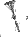
- FIG. 3 is a diagram of an example optical device 300 including two scanners and a lens system as described herein.
- the optical device 300 may include scanner 1 , scanner 2 , and a lens system including lens 1 and lens 2 .
- scanner 1 , scanner 2 , the lens system, lens 1 , and lens 2 of the optical device 300 may be similar to scanner 1 , scanner 2 , the lens system, lens 1 , and lens 2 of the optical device 200 of FIG. 2 .
- FIG. 3 is a diagram of an example optical device 300 including two scanners and a lens system as described herein.
- the optical device 300 may include scanner 1 , scanner 2 , and a lens system including lens 1 and lens 2 .
- scanner 1 , scanner 2 , the lens system, lens 1 , and lens 2 of the optical device 300 may be similar to scanner 1 , scanner 2 , the lens system, lens 1 , and lens 2 of the optical device 200 of FIG. 2 .
- FIG. 1 is a diagram of an example optical device 300 including two scanners and
- the optical device 300 may combine the vertical angular offset provided by scanner 1 and the horizontal angular offset provided by scanner 2 to scan a field of view in two dimensions (e.g., a two-dimensional field of view).
- the optical device 300 may conserve power resources, financial resources, and/or the like that would otherwise be consumed by using a dual-axis angular scanning component to scan a field of view in two dimensions.
- the lens system may include a beam expander to increase the size of the optical beam.
- a combination of lens 1 and lens 2 may be the beam expander.
- lens 1 may receive, from scanner 1 , a collimated optical beam having an initial size.
- lens 1 and lens 2 may be positioned such that a distance between lens 1 and lens 2 is equal to the sum of the focal length f 1 of lens 1 and the focal length f 2 of lens 2 .
- the optical beam decreases in size and then increases to a size greater than the initial size.
- FIG. 4 shows that between lens 1 and lens 2 , the optical beam decreases in size and then increases to a size greater than the initial size.
- FIG. 5 is a diagram of an example optical device 500 including a scanner, a lens system, and a window and an example optical device 510 including a scanner and a window.
- the optical device 500 may include a scanner, a lens system including lens 1 and lens 2 , and a window.
- the scanner, the lens system, lens 1 , and lens 2 of the optical device 500 may be similar to scanner 1 , the lens system, lens 1 , and lens 2 of the optical device 200 of FIG. 2 .
- the optical device 510 may include a scanner and a window.
- the scanner of the optical device 510 may be similar to scanner 1 and/or scanner 2 of the optical device 200 of FIG. 2 .
- the scanner of the optical device 510 may be similar to the scanner of the optical device 500 (e.g., have a same size, tilt angle, axis of orientation, axes of orientation, and/or the like).
- the scanner of optical device 500 and the scanner of optical device 510 may be single-axis angular scanning components having horizontal axes to provide vertical angular offsets.
- the window of the optical device 500 and the window of optical device 510 may be windows in a housing of a lidar optical subassembly, where the windows permit optical components (e.g., the scanner, lens 1 , lens 2 , one or more receivers, and/or the like) within the lidar optical subassembly to optically communicate with an environment external to the housing.
- the windows may transmit light, be scratch-resistant, and protect the components of the optical device 500 and/or the optical device 510 .
- the windows may include a glass substrate, a sapphire substrate, and/or the like.
- the window of the optical device 500 and the window of the optical device 510 may permit the scanners to scan the optical beams across fields of view having a same height.
- the window of the optical device 500 may be smaller than the window of the optical device 510 .
- the window of the optical device 510 may be larger than the scanner to accommodate the vertical angular offset provided to the optical beam by the scanner.
- the window of optical device 500 may be of similar size to the scanner because the lens system (e.g., lens 1 and lens 2 ) achieves a 1:1 image of the scanner on the window. For example, if a focal length f 1 of lens 1 equals a focal length f 2 of lens 2 , then the lens system achieves a 1:1 image of the scanner on the window.
- the optical device 500 may include a lens system configured to increase a size of the optical beam.
- the optical device 500 may include a lens system that includes a beam expander to increase the size of the optical beam (e.g., before passing through the window) and achieve a higher resolution than may be achieved with the small beam size.
- the increased beam size may permit the optical device 500 to obtain more information regarding objects in the field of view than may be obtained with a small beam size.
- an optical device may include a lens system configured to increase and/or decrease a size of the optical beam.
- the increase and/or decrease may be described as a beam expansion ratio (e.g., in the case of an increase in the size of the optical beam) or a beam reduction ratio (e.g., in the case of a decrease in the size of the optical beam).
- an optical device may include a scanner and a lens system and may use the beam expansion ratio or the beam reduction ratio of the lens system to tradeoff tilting angle and scanner mirror size while maintaining the resonant frequency of the scanner.
- the lens system may have a beam expansion ratio of 2 (e.g., the optical beam is twice as big after passing through the lens system and/or the like), and the scanner may have a tilting angle that is reduced by half based on the beam expansion ratio and may also have a scanner mirror size that is reduced by half based on the beam expansion ratio.
- the scanner may have an increased resonant frequency due to the reduced tilting angle and reduced scanner mirror size, which may improve performance of the optical device.
- the reduced tilting angle may result in a reduction in performance of the optical device
- the reduced scanner mirror size may result in a performance improvement greater than the reduction in performance resulting from the reduced tilting angle.
- FIG. 6A is a diagram of an example graph 610 showing field distortion.
- optical components e.g., a scanner, a lens system, and/or the like
- combinations of optical components within an optical device e.g., optical device 100 , optical device 200 , optical device 300 , optical device 400 , optical device 500 , optical device 510 , and/or the like
- the scan lines of the optical device may be curved.
- FIG. 6B is a diagram of an example adjustment 620 to a scanner to compensate for the field distortion in the optical device of FIG. 6A .
- the scanner of FIG. 6B may be a dual-axis angular scanning component having a y axis (e.g., a horizontal axis) to provide a vertical angular offset and an x axis (e.g., a vertical axis) to provide a horizontal angular offset.
- the optical device may adjust a tilting angle of the scanner on they axis and/or adjust a tilting angle of the scanner on the x axis to compensate for the field distortion and/or achieve linear scan lines.
- the optical device may adjust the tilting angle of the scanner on the y axis by 5 degrees and adjust the tilting angle of the scanner on the x axis by 12.5 degrees. In this way, the optical device may adjust the angle at which an incoming optical beam (e.g., shown as in (I)) is reflected by the scanner as an outgoing optical beam (e.g., shown as out (O)) to compensate for the field distortion and/or achieve linear scan line.
- an incoming optical beam e.g., shown as in (I)
- an outgoing optical beam e.g., shown as out (O)
- the optical device may include a first scanner and a second scanner, where the first scanner and the second scanner are dual-axis angular scanning components.
- the first scanner and/or the second scanner may be configured to compensate for field distortion of the optical beam.
- the optical device may adjust the first scanner and/or the second scanner to compensate for field distortion. For example, the optical device may adjust the first scanner to compensate for field distortion caused by optical components positioned between a source of the optical beam and the first scanner and may adjust the second scanner to compensate for field distortion caused by optical components positioned between the first scanner and the second scanner.
- FIG. 7 is a diagram of an example optical device 700 including two scanners and a lens system.
- the optical device 700 may include scanner 1 , scanner 2 , and a lens system including lens 1 and lens 2 as well as a filter and/or a diffractive optical element (DOE).
- DOE diffractive optical element
- scanner 1 , scanner 2 , the lens system, lens 1 , and lens 2 of the optical device 700 may be similar to scanner 1 , scanner 2 , the lens system, lens 1 , and lens 2 of the optical device 200 of FIG. 2 .
- the lens system may include the filter and/or the DOE in a location where the size of the optical beam is small relative to the filter and/or the DOE.
- the filter and/or the DOE may be positioned between lens 1 and lens 2 .
- the filter and/or the DOE may be positioned at a location corresponding to a focal point of lens 1 and a focal point of lens 2 .
- the optical device 700 may improve the performance of the filter and/or the DOE when providing angular dependent modification to the optical beam, field distortion compensation and/or correction to the optical beam, and/or the like.
- component is intended to be broadly construed as hardware, firmware, and/or a combination of hardware and software.
- the terms “has,” “have,” “having,” or the like are intended to be open-ended terms. Further, the phrase “based on” is intended to mean “based, at least in part, on” unless explicitly stated otherwise. Also, as used herein, the term “or” is intended to be inclusive when used in a series and may be used interchangeably with “and/or,” unless explicitly stated otherwise (e.g., if used in combination with “either” or “only one of”).
Landscapes
- Physics & Mathematics (AREA)
- Engineering & Computer Science (AREA)
- General Physics & Mathematics (AREA)
- Computer Networks & Wireless Communication (AREA)
- Radar, Positioning & Navigation (AREA)
- Remote Sensing (AREA)
- Optics & Photonics (AREA)
- Electromagnetism (AREA)
- Mechanical Optical Scanning Systems (AREA)
- Lenses (AREA)
Abstract
Description
f1/f2=s1/s2=a2/a1.
In some implementations, if the focal length f1 of
Claims (20)
Priority Applications (3)
| Application Number | Priority Date | Filing Date | Title |
|---|---|---|---|
| US16/725,603 US11500070B2 (en) | 2019-09-04 | 2019-12-23 | Optical device having two scanning components, one configured to compensate for field distortion |
| CN202010618535.0A CN112526541B (en) | 2019-09-04 | 2020-06-30 | Optical device with two scanning assemblies |
| US18/054,969 US11906666B2 (en) | 2019-09-04 | 2022-11-14 | Optical device having two scanning components |
Applications Claiming Priority (2)
| Application Number | Priority Date | Filing Date | Title |
|---|---|---|---|
| US201962895744P | 2019-09-04 | 2019-09-04 | |
| US16/725,603 US11500070B2 (en) | 2019-09-04 | 2019-12-23 | Optical device having two scanning components, one configured to compensate for field distortion |
Related Child Applications (1)
| Application Number | Title | Priority Date | Filing Date |
|---|---|---|---|
| US18/054,969 Continuation US11906666B2 (en) | 2019-09-04 | 2022-11-14 | Optical device having two scanning components |
Publications (2)
| Publication Number | Publication Date |
|---|---|
| US20210063542A1 US20210063542A1 (en) | 2021-03-04 |
| US11500070B2 true US11500070B2 (en) | 2022-11-15 |
Family
ID=74679674
Family Applications (2)
| Application Number | Title | Priority Date | Filing Date |
|---|---|---|---|
| US16/725,603 Active 2041-01-19 US11500070B2 (en) | 2019-09-04 | 2019-12-23 | Optical device having two scanning components, one configured to compensate for field distortion |
| US18/054,969 Active 2039-12-23 US11906666B2 (en) | 2019-09-04 | 2022-11-14 | Optical device having two scanning components |
Family Applications After (1)
| Application Number | Title | Priority Date | Filing Date |
|---|---|---|---|
| US18/054,969 Active 2039-12-23 US11906666B2 (en) | 2019-09-04 | 2022-11-14 | Optical device having two scanning components |
Country Status (2)
| Country | Link |
|---|---|
| US (2) | US11500070B2 (en) |
| CN (1) | CN112526541B (en) |
Cited By (2)
| Publication number | Priority date | Publication date | Assignee | Title |
|---|---|---|---|---|
| US11906666B2 (en) | 2019-09-04 | 2024-02-20 | Lumentum Operations Llc | Optical device having two scanning components |
| US20240183950A1 (en) * | 2022-12-06 | 2024-06-06 | Cepton Technologies, Inc. | Scanning lidar with discrete vertical steps |
Families Citing this family (12)
| Publication number | Priority date | Publication date | Assignee | Title |
|---|---|---|---|---|
| US11536805B2 (en) | 2018-06-25 | 2022-12-27 | Silc Technologies, Inc. | Optical switching for tuning direction of LIDAR output signals |
| US12535586B2 (en) | 2018-08-31 | 2026-01-27 | SiLC Technology, Inc. | Reduction of ADC sampling rates in LIDAR systems |
| US12429569B2 (en) | 2019-05-17 | 2025-09-30 | Silc Technologies, Inc. | Identification of materials illuminated by LIDAR systems |
| US11650317B2 (en) | 2019-06-28 | 2023-05-16 | Silc Technologies, Inc. | Use of frequency offsets in generation of LIDAR data |
| US11789154B2 (en) * | 2020-07-17 | 2023-10-17 | Silc Technologies, Inc. | Walk-off compensation in remote imaging systems |
| US12541009B2 (en) | 2021-06-17 | 2026-02-03 | Silc Technologies, Inc. | Scanning multiple LIDAR system output signals |
| US12411213B2 (en) | 2021-10-11 | 2025-09-09 | Silc Technologies, Inc. | Separation of light signals in a LIDAR system |
| US12553995B2 (en) | 2022-02-14 | 2026-02-17 | Silc Technologies, Inc. | Data refinement in optical systems |
| US12578443B2 (en) | 2022-04-23 | 2026-03-17 | Silc Technologies, Inc. | Data refinement in optical imaging systems |
| US12663516B2 (en) | 2022-07-08 | 2026-06-23 | Silc Technologies, Inc. | Imaging system with enhanced scan rate |
| US12422618B2 (en) | 2022-10-13 | 2025-09-23 | Silc Technologies, Inc. | Buried taper with reflecting surface |
| US12578439B2 (en) | 2023-04-11 | 2026-03-17 | Silc Technologies, Inc. | Increasing resolution in imaging systems |
Citations (3)
| Publication number | Priority date | Publication date | Assignee | Title |
|---|---|---|---|---|
| US20110242635A1 (en) * | 2010-03-31 | 2011-10-06 | Brother Kogyo Kabushiki Kaisha | Head-Mounted Display |
| US20160187646A1 (en) * | 2014-12-29 | 2016-06-30 | Jonathan S. Ehrmann | High-speed optical scanning systems and methods |
| US20170052366A1 (en) * | 2015-08-18 | 2017-02-23 | Seiko Epson Corporation | Optical scanner, image display device, and head mounted display |
Family Cites Families (9)
| Publication number | Priority date | Publication date | Assignee | Title |
|---|---|---|---|---|
| JP4159738B2 (en) * | 2000-11-07 | 2008-10-01 | 株式会社小松製作所 | Beam scanning laser marking system |
| KR20060016545A (en) | 2004-08-18 | 2006-02-22 | 삼성전자주식회사 | Beam scanning optical system |
| WO2009069382A1 (en) | 2007-11-28 | 2009-06-04 | Nec Corporation | Optical scanning device and image outputting device |
| CN101430377B (en) * | 2008-11-18 | 2011-06-22 | 北京航空航天大学 | APD array-based non-scanning 3D imaging lidar optical system |
| DE102013106533A1 (en) | 2013-06-21 | 2014-12-24 | Jenoptik Optical Systems Gmbh | scanning device |
| WO2016134321A1 (en) | 2015-02-20 | 2016-08-25 | Apple Inc. | Actuated optical element for light beam scanning device |
| US10502546B2 (en) * | 2017-11-07 | 2019-12-10 | Santec Corporation | Systems and methods for variable-range fourier domain imaging |
| CN121679522A (en) * | 2018-06-12 | 2026-03-17 | 深圳市镭神智能系统有限公司 | Micro-mirror scanning optical system |
| US11500070B2 (en) | 2019-09-04 | 2022-11-15 | Lumentum Operations Llc | Optical device having two scanning components, one configured to compensate for field distortion |
-
2019
- 2019-12-23 US US16/725,603 patent/US11500070B2/en active Active
-
2020
- 2020-06-30 CN CN202010618535.0A patent/CN112526541B/en active Active
-
2022
- 2022-11-14 US US18/054,969 patent/US11906666B2/en active Active
Patent Citations (3)
| Publication number | Priority date | Publication date | Assignee | Title |
|---|---|---|---|---|
| US20110242635A1 (en) * | 2010-03-31 | 2011-10-06 | Brother Kogyo Kabushiki Kaisha | Head-Mounted Display |
| US20160187646A1 (en) * | 2014-12-29 | 2016-06-30 | Jonathan S. Ehrmann | High-speed optical scanning systems and methods |
| US20170052366A1 (en) * | 2015-08-18 | 2017-02-23 | Seiko Epson Corporation | Optical scanner, image display device, and head mounted display |
Cited By (2)
| Publication number | Priority date | Publication date | Assignee | Title |
|---|---|---|---|---|
| US11906666B2 (en) | 2019-09-04 | 2024-02-20 | Lumentum Operations Llc | Optical device having two scanning components |
| US20240183950A1 (en) * | 2022-12-06 | 2024-06-06 | Cepton Technologies, Inc. | Scanning lidar with discrete vertical steps |
Also Published As
| Publication number | Publication date |
|---|---|
| CN112526541B (en) | 2023-07-25 |
| US20230146243A1 (en) | 2023-05-11 |
| US20210063542A1 (en) | 2021-03-04 |
| US11906666B2 (en) | 2024-02-20 |
| CN112526541A (en) | 2021-03-19 |
Similar Documents
| Publication | Publication Date | Title |
|---|---|---|
| US11906666B2 (en) | Optical device having two scanning components | |
| US9348138B2 (en) | Laser processing device | |
| JP3193546B2 (en) | Reflective scanning optical system | |
| US9250438B2 (en) | Freeform surface reflective scanning system | |
| US9122039B2 (en) | Compact internal field of view switch and pupil relay | |
| US10690903B2 (en) | Optical configurations for optical field mappings for back-scanned and line-scanned imagers | |
| US4936643A (en) | Light scanner | |
| EP3514575A2 (en) | Light emission apparatus, object information detection apparatus, optical path adjustment method, object information detection method, and light modulation unit | |
| EP0454503B1 (en) | Optical scanners | |
| KR101924540B1 (en) | Alignment Method for Off-axis Reflective Optical System | |
| US8358457B2 (en) | Miniature rotating transmissive optical drum scanner | |
| Nan et al. | Uncertainty analysis and optimization design of long-distance laser triangulation displacement sensor applied to dynamic object | |
| US6703634B2 (en) | 3D-shape measurement apparatus | |
| US10812195B2 (en) | Optical communication device | |
| KR20230041973A (en) | Lidar MEMS angle adjustment | |
| JP2002062499A (en) | Scanning optical device | |
| WO2021125018A1 (en) | Light emitting device, object detecting device, and mobile body | |
| US6515783B2 (en) | Penta assembly skew compensator | |
| JPH01309021A (en) | Light beam scanning optical system | |
| CN113260893A (en) | Optical system | |
| WO2023216157A1 (en) | A camera module comprising an image rotation correction mechanism and an optical element having dach reflective surfaces thereof | |
| US20250147304A1 (en) | Optical scanning system | |
| JPH07174996A (en) | Raster output scanner image system | |
| EP0828173A3 (en) | Optical scanning apparatus | |
| US7054046B2 (en) | Optical scanning frequency doubling method and apparatus adopting the same |
Legal Events
| Date | Code | Title | Description |
|---|---|---|---|
| AS | Assignment |
Owner name: LUMENTUM OPERATIONS LLC, CALIFORNIA Free format text: ASSIGNMENT OF ASSIGNORS INTEREST;ASSIGNORS:ZHENG, JIAMIN;KEYWORTH, BARRIE P.;JIN, WENLIN;SIGNING DATES FROM 20191221 TO 20191223;REEL/FRAME:051358/0861 |
|
| FEPP | Fee payment procedure |
Free format text: ENTITY STATUS SET TO UNDISCOUNTED (ORIGINAL EVENT CODE: BIG.); ENTITY STATUS OF PATENT OWNER: LARGE ENTITY |
|
| STPP | Information on status: patent application and granting procedure in general |
Free format text: APPLICATION DISPATCHED FROM PREEXAM, NOT YET DOCKETED |
|
| STPP | Information on status: patent application and granting procedure in general |
Free format text: DOCKETED NEW CASE - READY FOR EXAMINATION |
|
| STPP | Information on status: patent application and granting procedure in general |
Free format text: NON FINAL ACTION MAILED |
|
| STPP | Information on status: patent application and granting procedure in general |
Free format text: NOTICE OF ALLOWANCE MAILED -- APPLICATION RECEIVED IN OFFICE OF PUBLICATIONS |
|
| STPP | Information on status: patent application and granting procedure in general |
Free format text: PUBLICATIONS -- ISSUE FEE PAYMENT RECEIVED |
|
| STCF | Information on status: patent grant |
Free format text: PATENTED CASE |
|
| AS | Assignment |
Owner name: WELLS FARGO BANK, NATIONAL ASSOCIATION, AS COLLATERAL AGENT, NORTH CAROLINA Free format text: ASSIGNMENT OF ASSIGNORS INTEREST;ASSIGNOR:LUMENTUM OPERATIONS LLC;REEL/FRAME:074974/0001 Effective date: 20251219 |
|
| MAFP | Maintenance fee payment |
Free format text: PAYMENT OF MAINTENANCE FEE, 4TH YEAR, LARGE ENTITY (ORIGINAL EVENT CODE: M1551); ENTITY STATUS OF PATENT OWNER: LARGE ENTITY Year of fee payment: 4 |