US11476247B2 - Semiconductor rectifier - Google Patents
Semiconductor rectifier Download PDFInfo
- Publication number
- US11476247B2 US11476247B2 US16/767,428 US201816767428A US11476247B2 US 11476247 B2 US11476247 B2 US 11476247B2 US 201816767428 A US201816767428 A US 201816767428A US 11476247 B2 US11476247 B2 US 11476247B2
- Authority
- US
- United States
- Prior art keywords
- electrode
- semiconductor rectifier
- diode
- transistor
- semiconductor
- Prior art date
- Legal status (The legal status is an assumption and is not a legal conclusion. Google has not performed a legal analysis and makes no representation as to the accuracy of the status listed.)
- Active, expires
Links
Images


Classifications
-
- H01L27/0629—
-
- H—ELECTRICITY
- H10—SEMICONDUCTOR DEVICES; ELECTRIC SOLID-STATE DEVICES NOT OTHERWISE PROVIDED FOR
- H10D—INORGANIC ELECTRIC SEMICONDUCTOR DEVICES
- H10D84/00—Integrated devices formed in or on semiconductor substrates that comprise only semiconducting layers, e.g. on Si wafers or on GaAs-on-Si wafers
- H10D84/80—Integrated devices formed in or on semiconductor substrates that comprise only semiconducting layers, e.g. on Si wafers or on GaAs-on-Si wafers characterised by the integration of at least one component covered by groups H10D12/00 or H10D30/00, e.g. integration of IGFETs
- H10D84/811—Combinations of field-effect devices and one or more diodes, capacitors or resistors
-
- H—ELECTRICITY
- H10—SEMICONDUCTOR DEVICES; ELECTRIC SOLID-STATE DEVICES NOT OTHERWISE PROVIDED FOR
- H10W—GENERIC PACKAGES, INTERCONNECTIONS, CONNECTORS OR OTHER CONSTRUCTIONAL DETAILS OF DEVICES COVERED BY CLASS H10
- H10W70/00—Package substrates; Interposers; Redistribution layers [RDL]
- H10W70/40—Leadframes
- H10W70/464—Additional interconnections in combination with leadframes
- H10W70/468—Circuit boards
-
- H01L29/1608—
-
- H01L29/2003—
-
- H01L29/872—
-
- H—ELECTRICITY
- H02—GENERATION; CONVERSION OR DISTRIBUTION OF ELECTRIC POWER
- H02M—APPARATUS FOR CONVERSION BETWEEN AC AND AC, BETWEEN AC AND DC, OR BETWEEN DC AND DC, AND FOR USE WITH MAINS OR SIMILAR POWER SUPPLY SYSTEMS; CONVERSION OF DC OR AC INPUT POWER INTO SURGE OUTPUT POWER; CONTROL OR REGULATION THEREOF
- H02M7/00—Conversion of AC power input into DC power output; Conversion of DC power input into AC power output
- H02M7/02—Conversion of AC power input into DC power output without possibility of reversal
- H02M7/04—Conversion of AC power input into DC power output without possibility of reversal by static converters
- H02M7/12—Conversion of AC power input into DC power output without possibility of reversal by static converters using discharge tubes with control electrode or semiconductor devices with control electrode
-
- H—ELECTRICITY
- H10—SEMICONDUCTOR DEVICES; ELECTRIC SOLID-STATE DEVICES NOT OTHERWISE PROVIDED FOR
- H10D—INORGANIC ELECTRIC SEMICONDUCTOR DEVICES
- H10D62/00—Semiconductor bodies, or regions thereof, of devices having potential barriers
- H10D62/80—Semiconductor bodies, or regions thereof, of devices having potential barriers characterised by the materials
- H10D62/83—Semiconductor bodies, or regions thereof, of devices having potential barriers characterised by the materials being Group IV materials, e.g. B-doped Si or undoped Ge
- H10D62/832—Semiconductor bodies, or regions thereof, of devices having potential barriers characterised by the materials being Group IV materials, e.g. B-doped Si or undoped Ge being Group IV materials comprising two or more elements, e.g. SiGe
- H10D62/8325—Silicon carbide
-
- H—ELECTRICITY
- H10—SEMICONDUCTOR DEVICES; ELECTRIC SOLID-STATE DEVICES NOT OTHERWISE PROVIDED FOR
- H10D—INORGANIC ELECTRIC SEMICONDUCTOR DEVICES
- H10D62/00—Semiconductor bodies, or regions thereof, of devices having potential barriers
- H10D62/80—Semiconductor bodies, or regions thereof, of devices having potential barriers characterised by the materials
- H10D62/85—Semiconductor bodies, or regions thereof, of devices having potential barriers characterised by the materials being Group III-V materials, e.g. GaAs
- H10D62/8503—Nitride Group III-V materials, e.g. AlN or GaN
-
- H—ELECTRICITY
- H10—SEMICONDUCTOR DEVICES; ELECTRIC SOLID-STATE DEVICES NOT OTHERWISE PROVIDED FOR
- H10D—INORGANIC ELECTRIC SEMICONDUCTOR DEVICES
- H10D8/00—Diodes
- H10D8/60—Schottky-barrier diodes
-
- H—ELECTRICITY
- H10—SEMICONDUCTOR DEVICES; ELECTRIC SOLID-STATE DEVICES NOT OTHERWISE PROVIDED FOR
- H10W—GENERIC PACKAGES, INTERCONNECTIONS, CONNECTORS OR OTHER CONSTRUCTIONAL DETAILS OF DEVICES COVERED BY CLASS H10
- H10W70/00—Package substrates; Interposers; Redistribution layers [RDL]
- H10W70/40—Leadframes
- H10W70/481—Leadframes for devices being provided for in groups H10D8/00 - H10D48/00
-
- H—ELECTRICITY
- H10—SEMICONDUCTOR DEVICES; ELECTRIC SOLID-STATE DEVICES NOT OTHERWISE PROVIDED FOR
- H10W—GENERIC PACKAGES, INTERCONNECTIONS, CONNECTORS OR OTHER CONSTRUCTIONAL DETAILS OF DEVICES COVERED BY CLASS H10
- H10W90/00—Package configurations
- H10W90/811—Multiple chips on leadframes
-
- H—ELECTRICITY
- H10—SEMICONDUCTOR DEVICES; ELECTRIC SOLID-STATE DEVICES NOT OTHERWISE PROVIDED FOR
- H10W—GENERIC PACKAGES, INTERCONNECTIONS, CONNECTORS OR OTHER CONSTRUCTIONAL DETAILS OF DEVICES COVERED BY CLASS H10
- H10W70/00—Package substrates; Interposers; Redistribution layers [RDL]
- H10W70/40—Leadframes
- H10W70/464—Additional interconnections in combination with leadframes
- H10W70/465—Bumps or wires
-
- H—ELECTRICITY
- H10—SEMICONDUCTOR DEVICES; ELECTRIC SOLID-STATE DEVICES NOT OTHERWISE PROVIDED FOR
- H10W—GENERIC PACKAGES, INTERCONNECTIONS, CONNECTORS OR OTHER CONSTRUCTIONAL DETAILS OF DEVICES COVERED BY CLASS H10
- H10W72/00—Interconnections or connectors in packages
- H10W72/50—Bond wires
- H10W72/541—Dispositions of bond wires
- H10W72/547—Dispositions of multiple bond wires
- H10W72/5475—Dispositions of multiple bond wires multiple bond wires connected to common bond pads at both ends of the wires
-
- H—ELECTRICITY
- H10—SEMICONDUCTOR DEVICES; ELECTRIC SOLID-STATE DEVICES NOT OTHERWISE PROVIDED FOR
- H10W—GENERIC PACKAGES, INTERCONNECTIONS, CONNECTORS OR OTHER CONSTRUCTIONAL DETAILS OF DEVICES COVERED BY CLASS H10
- H10W72/00—Interconnections or connectors in packages
- H10W72/851—Dispositions of multiple connectors or interconnections
- H10W72/874—On different surfaces
- H10W72/884—Die-attach connectors and bond wires
-
- H—ELECTRICITY
- H10—SEMICONDUCTOR DEVICES; ELECTRIC SOLID-STATE DEVICES NOT OTHERWISE PROVIDED FOR
- H10W—GENERIC PACKAGES, INTERCONNECTIONS, CONNECTORS OR OTHER CONSTRUCTIONAL DETAILS OF DEVICES COVERED BY CLASS H10
- H10W72/00—Interconnections or connectors in packages
- H10W72/90—Bond pads, in general
- H10W72/921—Structures or relative sizes of bond pads
- H10W72/926—Multiple bond pads having different sizes
-
- H—ELECTRICITY
- H10—SEMICONDUCTOR DEVICES; ELECTRIC SOLID-STATE DEVICES NOT OTHERWISE PROVIDED FOR
- H10W—GENERIC PACKAGES, INTERCONNECTIONS, CONNECTORS OR OTHER CONSTRUCTIONAL DETAILS OF DEVICES COVERED BY CLASS H10
- H10W72/00—Interconnections or connectors in packages
- H10W72/90—Bond pads, in general
- H10W72/941—Dispositions of bond pads
- H10W72/944—Dispositions of multiple bond pads
-
- H—ELECTRICITY
- H10—SEMICONDUCTOR DEVICES; ELECTRIC SOLID-STATE DEVICES NOT OTHERWISE PROVIDED FOR
- H10W—GENERIC PACKAGES, INTERCONNECTIONS, CONNECTORS OR OTHER CONSTRUCTIONAL DETAILS OF DEVICES COVERED BY CLASS H10
- H10W74/00—Encapsulations, e.g. protective coatings
-
- H—ELECTRICITY
- H10—SEMICONDUCTOR DEVICES; ELECTRIC SOLID-STATE DEVICES NOT OTHERWISE PROVIDED FOR
- H10W—GENERIC PACKAGES, INTERCONNECTIONS, CONNECTORS OR OTHER CONSTRUCTIONAL DETAILS OF DEVICES COVERED BY CLASS H10
- H10W90/00—Package configurations
- H10W90/701—Package configurations characterised by the relative positions of pads or connectors relative to package parts
- H10W90/731—Package configurations characterised by the relative positions of pads or connectors relative to package parts of die-attach connectors
- H10W90/732—Package configurations characterised by the relative positions of pads or connectors relative to package parts of die-attach connectors between stacked chips
-
- H—ELECTRICITY
- H10—SEMICONDUCTOR DEVICES; ELECTRIC SOLID-STATE DEVICES NOT OTHERWISE PROVIDED FOR
- H10W—GENERIC PACKAGES, INTERCONNECTIONS, CONNECTORS OR OTHER CONSTRUCTIONAL DETAILS OF DEVICES COVERED BY CLASS H10
- H10W90/00—Package configurations
- H10W90/701—Package configurations characterised by the relative positions of pads or connectors relative to package parts
- H10W90/751—Package configurations characterised by the relative positions of pads or connectors relative to package parts of bond wires
- H10W90/752—Package configurations characterised by the relative positions of pads or connectors relative to package parts of bond wires between stacked chips
-
- H—ELECTRICITY
- H10—SEMICONDUCTOR DEVICES; ELECTRIC SOLID-STATE DEVICES NOT OTHERWISE PROVIDED FOR
- H10W—GENERIC PACKAGES, INTERCONNECTIONS, CONNECTORS OR OTHER CONSTRUCTIONAL DETAILS OF DEVICES COVERED BY CLASS H10
- H10W90/00—Package configurations
- H10W90/701—Package configurations characterised by the relative positions of pads or connectors relative to package parts
- H10W90/751—Package configurations characterised by the relative positions of pads or connectors relative to package parts of bond wires
- H10W90/753—Package configurations characterised by the relative positions of pads or connectors relative to package parts of bond wires between laterally-adjacent chips
-
- H—ELECTRICITY
- H10—SEMICONDUCTOR DEVICES; ELECTRIC SOLID-STATE DEVICES NOT OTHERWISE PROVIDED FOR
- H10W—GENERIC PACKAGES, INTERCONNECTIONS, CONNECTORS OR OTHER CONSTRUCTIONAL DETAILS OF DEVICES COVERED BY CLASS H10
- H10W90/00—Package configurations
- H10W90/701—Package configurations characterised by the relative positions of pads or connectors relative to package parts
- H10W90/751—Package configurations characterised by the relative positions of pads or connectors relative to package parts of bond wires
- H10W90/756—Package configurations characterised by the relative positions of pads or connectors relative to package parts of bond wires between a chip and a stacked lead frame, conducting package substrate or heat sink
Definitions
- the present disclosure relates to a semiconductor rectifier.
- a Schottky barrier diode which is a type of semiconductor rectifier, includes a silicon semiconductor layer, a Schottky electrode, and an ohmic electrode.
- the present disclosure provides a semiconductor rectifier including a transistor and a diode.
- the transistor includes a source electrode, a drain electrode and a gate electrode.
- the diode includes an anode electrode and a cathode electrode. The anode electrode is electrically connected to the gate electrode, and the cathode electrode is electrically connected to the source electrode.
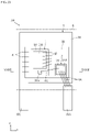
- FIG. 1 is a plan view showing a semiconductor rectifier according to a first embodiment of the present disclosure.
- FIG. 2 is a cross-sectional view taken along a line II-II in FIG. 1 .
- FIG. 3 is a cross-sectional view taken along a line III-III in FIG. 1 .
- FIG. 4 is a circuit diagram of the semiconductor rectifier according to the first embodiment of the present disclosure.
- FIG. 5 is a graph showing voltage-current characteristics of the semiconductor rectifier according to the first embodiment of the present disclosure.
- FIG. 6 is a graph showing reverse recovery characteristics of the semiconductor rectifier according to the first embodiment of the present disclosure.
- FIG. 7 is a plan view showing a first variation of the semiconductor rectifier according to the first embodiment of the present disclosure.
- FIG. 8 is a plan view showing a second variation of the semiconductor rectifier according to the first embodiment of the present disclosure.
- FIG. 9 is a cross-sectional view taken along a line IX-IX in FIG. 8 .
- FIG. 10 is a plan view showing a third variation of the semiconductor rectifier according to the first embodiment of the present disclosure.
- FIG. 11 is a plan view showing a semiconductor rectifier according to a second embodiment of the present disclosure.
- FIG. 12 is a circuit diagram of the semiconductor rectifier according to the second embodiment of the present disclosure.
- FIG. 13 is a plan view showing a semiconductor rectifier according to a third embodiment of the present disclosure.
- FIG. 14 is a circuit diagram of the semiconductor rectifier according to the third embodiment of the present disclosure.
- FIG. 15 is a plan view showing a first variation of the semiconductor rectifier according to the third embodiment of the present disclosure.
- FIG. 16 is a circuit diagram of the first variation of the semiconductor rectifier according to the third embodiment of the present disclosure.
- FIG. 17 is a graph showing the reverse recovery characteristics of the semiconductor rectifier according to the first embodiment of the present disclosure.
- FIG. 18 is a graph showing diode voltages of the semiconductor rectifier according to the first embodiment of the present disclosure.
- FIG. 19 is a graph showing the reverse recovery characteristics of the semiconductor rectifier according to the third embodiment of the present disclosure.
- FIG. 20 is a graph showing the diode voltages of the semiconductor rectifier according to the third embodiment of the present disclosure.
- FIG. 21 is a plan view showing a semiconductor rectifier according to a fourth embodiment of the present disclosure.
- FIG. 22 is a cross-sectional view taken along a line XXII-XXII in FIG. 21 .
- FIG. 23 is a plan view showing a first variation of the semiconductor rectifier according to the fourth embodiment of the present disclosure.
- FIG. 24 is a plan view showing a second variation of the semiconductor rectifier according to the fourth embodiment of the present disclosure.
- FIG. 25 is a cross-sectional view taken along a line XXV-XXV in FIG. 24 .
- FIG. 26 is a plan view showing a semiconductor rectifier according to a fifth embodiment of the present disclosure.
- FIG. 27 is a circuit diagram of the semiconductor rectifier according to the fifth embodiment of the present disclosure.
- FIG. 28 is a plan view showing a semiconductor rectifier according to a sixth embodiment of the present disclosure.
- FIG. 29 is a cross-sectional view taken along a line XXIX-XXIX in FIG. 28 .
- FIG. 30 is a plan view showing a semiconductor rectifier according to a seventh embodiment of the present disclosure.
- FIG. 31 is a cross-sectional view taken along a line XXXI-XXXI in FIG. 30 .
- FIG. 1 to FIG. 4 illustrate a semiconductor rectifier according to a first embodiment of the present disclosure.
- the semiconductor rectifier A 1 according to this embodiment includes a transistor 1 , a diode 2 , a lead frame 3 , and a sealing resin 6 .
- FIG. 1 is a plan view showing the semiconductor rectifier A 1 .
- FIG. 2 is a cross-sectional view taken along a line II-II in FIG. 1 .
- FIG. 3 is a cross-sectional view taken along a line III-III in FIG. 1 .
- FIG. 4 is a circuit diagram of the semiconductor rectifier A 1 .
- the transistor 1 is, for example, a normally-on transistor (depletion type), and includes a main body 10 , a source electrode 11 S, a drain electrode 11 D, and a gate electrode 11 G.
- the main body 10 includes a semiconductor layer and, in this embodiment, includes a GaN semiconductor layer.
- the transistor 1 may be, for example, a GaN-MOSFET or a GaN-HEMT.
- the source electrode 11 S, the drain electrode 11 D, and the gate electrode 11 G are located on the upper face of the main body 10 , in other words on the same face of the main body 10 .
- the source electrode 11 S, the drain electrode 11 D, and the gate electrode 11 G are made of a metal and formed by plating, for example. From the viewpoint of the quality of wire bonding and solder bonding, it is preferable that the respective surface layers of the source electrode 11 S, the drain electrode 11 D, and the gate electrode 11 G include Au.
- the respective portions of the source electrode 11 S, the drain electrode 11 D, and the gate electrode 11 G covered with the surface layer are, for example, formed of a metal such as Cu or Ni.
- the diode 2 includes a main body 20 , an anode electrode 21 A and a cathode electrode 21 C.
- the diode 2 is, for example, a Si-Schottky barrier diode, in which the main body 20 includes a Si semiconductor layer.
- the threshold voltage of the diode 2 is equal to or lower than 0.8 V.
- the lead frame 3 supports the transistor 1 and the diode 2 , and constitutes an electrical conduction path to the transistor 1 and the diode 2 .
- the lead frame 3 includes an island portion 30 , an anode terminal 31 A, and a cathode terminal 31 C.
- the lead frame 3 also includes a metal layer 32 and an insulation layer 33 .
- the material of the lead frame 3 is not particularly limited.
- the lead frame 3 may be formed, for example, by punching or bending a metal sheet material of Cu or Ni.
- the island portion 30 supports the transistor 1 and the diode 2 .
- the island portion 30 has a rectangular shape in a plan view, having four sides extending along an x-direction or a y-direction.
- the shape of the island portion 30 is not particularly limited.
- the island portion 30 includes a metal layer 32 .
- the metal layer 32 is formed of a metal appropriately selected from, for example, A 1 , Cu, or Ni, or an alloy of the cited metals.
- the metal layer 32 is fixed to the island portion 30 , via an insulation layer 33 .
- the insulation layer 33 is formed of an insulative material, such as a resin or a ceramic.
- the metal layer 32 is smaller than the island portion 30 , when viewed in the z-direction.
- the formation method of the metal layer 32 is not particularly limited.
- the metal layer 32 may be formed on the insulation layer 33 by plating, or the metal layer 32 formed in advance may be bonded to the island portion 30 , via the insulation layer 33 .
- the transistor 1 is bonded to the metal layer 32 , via a bonding layer 19 .
- the cathode electrode 21 C of the diode 2 is bonded to the metal layer 32 , via a bonding layer 29 .
- the bonding layer 19 may be either insulative or conductive.
- the bonding layer 29 is formed of a conductive material, such as solder. Accordingly, the cathode electrode 21 C of the diode 2 is electrically connected to the metal layer 32 .
- the anode terminal 31 A serves as a terminal of the semiconductor rectifier A 1 , and is connected to the anode.
- the anode terminal 31 A is spaced apart from the island portion 30 .
- the cathode terminal 31 C serves as a terminal of the semiconductor rectifier A 1 , and is connected to the cathode. In this embodiment, the cathode terminal 31 C is connected to the island portion 30 .
- the semiconductor rectifier A 1 includes a plurality of anode wires 4 A, a gate wire 4 G, a plurality of source wires 4 S, and a plurality of drain wires 4 D.
- the anode wires 4 A are connected between the anode terminal 31 A and the anode electrode 21 A of the diode 2 .
- the gate wire 4 G is connected between the anode electrode 21 A of the diode 2 and the gate electrode 11 G of the transistor 1 .
- the source wires 4 S are connected between the metal layer 32 and the source electrode 11 S of the transistor 1 .
- the drain wires 4 D are connected between the drain electrode 11 D of the transistor 1 and the island portion 30 .
- the anode wires 4 A, the gate wire 4 G, the source wires 4 S, and the drain wires 4 D are, for example, formed of a metal such as Au, A 1 , or Cu. In the following description it will be assumed that the anode wires 4 A, the gate wire 4 G, the source wires 4 S and the drain wires 4 D are formed of Au. The number of each kind of wires mentioned above may vary and be determined depending on the material.
- the circuit of the semiconductor rectifier A 1 may be illustrated as in FIG. 4 .
- the anode electrode 21 A of the diode 2 is electrically connected to the gate electrode 11 G, via the gate wire 4 G.
- the cathode electrode 21 C of the diode 2 is electrically connected to the source electrode 11 S, via the metal layer 32 and the source wires 4 S.
- the sealing resin 6 serves to protect the transistor 1 , the diode 2 , a part of the lead frame 3 , the anode wires 4 A, the gate wire 4 G, the source wires 4 S, and the drain wires 4 D.
- the sealing resin 6 is formed of an insulative resin such as an epoxy resin. In the illustrated example, the bottom face of the island portion 30 is exposed from the sealing resin 6 .
- the anode terminal 31 A and the cathode terminal 31 C protrude out in the same direction from a side face of the sealing resin 6 .
- the semiconductor rectifier A 1 provides the following advantageous effects.
- the use of transistor 1 contributes to improving the withstand voltage, compared with, for example, a semiconductor rectifier constituted of a single diode.
- FIG. 5 shows a relation between the voltage and the current applied between the anode terminal 31 A and the cathode terminal 31 C, together with other relations between the voltage and the current in a semiconductor rectifier with a single fast recovery diode (Si-FRD), and in a semiconductor rectifier with a single Schottky barrier diode (SiC-SBD) for comparison with the semiconductor rectifier A 1 .
- Si-FRD single fast recovery diode
- SiC-SBD Schottky barrier diode
- the threshold voltage at which a predetermined current starts to run in the semiconductor rectifier A 1 is lower than the threshold voltage of the semiconductor rectifier including the single Si-FRD and the semiconductor rectifier including the single SiC-SBD.
- FIG. 6 indicates reverse recovery characteristics of the semiconductor rectifier A 1 , and also the semiconductor rectifier including the single Si-FRD and the semiconductor rectifier including the single SiC-SBD, as comparative examples. Focusing on the reverse recovery time, during which the current runs in the reverse direction when the semiconductor rectifier is turned off from anon state, the reverse recovery time of the semiconductor rectifier A 1 is similar to that of the semiconductor rectifier including the single SiC-SBD, but significantly shorter than that of the semiconductor rectifier including the single Si-FRD. Therefore, the semiconductor rectifier A 1 contributes to improving the withstand voltage, reducing the threshold voltage, and shortening the reverse recovery time.
- FIG. 7 to FIG. 31 illustrate variations and other embodiments of the present disclosure.
- the elements same as or similar to those of the foregoing embodiment are given the same numeral.
- FIG. 7 illustrates a first variation of the semiconductor rectifier A 1 .
- a semiconductor rectifier A 11 according to this variation is different from the semiconductor rectifier A 1 , in the configuration of the lead frame 3 .
- the metal layer 32 and the insulation layer 33 are not provided on the island portion 30 .
- the main body 10 of the transistor 1 is bonded to the island portion 30 via the bonding layer 19
- the cathode electrode 21 C of the diode 2 is bonded to the island portion 30 , via the bonding layer 29 . Therefore, the island portion 30 is equipotential with the cathode electrode 21 C. Accordingly, the cathode terminal 31 C is spaced apart from the island portion 30 .
- the drain wires 4 D are connected between the drain electrode 11 D of the transistor 1 and the cathode terminal 31 C.
- the island portion 30 may be either partially exposed from the sealing resin 6 , or entirely covered with the sealing resin 6 .
- the withstand voltage can be improved, the threshold voltage can be lowered, and the reverse recovery time can be shortened.
- the metal layer 32 and the insulation layer 33 are excluded, the manufacturing cost can be reduced.
- FIG. 8 and FIG. 9 illustrate a second variation of the semiconductor rectifier A 1 .
- a semiconductor rectifier A 12 according to this variation is different from the foregoing examples, in the mounting structure of the diode 2 .
- the cathode electrode 21 C of the diode 2 is bonded to the source electrode 11 S of the transistor 1 , via the bonding layer 29 .
- the diode 2 is superposed on the transistor 1 .
- the withstand voltage can be improved, the threshold voltage can be lowered, and the reverse recovery time can be shortened.
- the bonding layer 29 serves as the only electrical conduction path between the cathode electrode 21 C of the diode 2 and the source electrode 11 S of the transistor 1 , and the source wires 4 S provided in the foregoing examples are excluded. Therefore, the resistance in the electrical conduction path leading to the source electrode 11 S can be reduced. Further, the size of the semiconductor rectifier A 12 in a z-direction view can be reduced.
- FIG. 10 illustrates a third variation of the semiconductor rectifier A 1 .
- a semiconductor rectifier A 13 according to this variation is similar to the semiconductor rectifier A 12 in the mounting structure of the transistor 1 and the diode 2 , and different from the semiconductor rectifier A 12 in the configuration of the lead frame 3 .
- the island portion 30 and the cathode terminal 31 C are formed as a unified body.
- the drain wires 4 D are connected between the drain electrode 11 D and the island portion 30 .
- the withstand voltage can be improved, the threshold voltage can be lowered, and the reverse recovery time can be shortened.
- the drain wires 4 D can be made shorter, compared with those of the semiconductor rectifier A 12 . Therefore, the resistance in the electrical conduction path between the drain electrode 11 D and the cathode terminal 31 C can be reduced.
- FIG. 11 and FIG. 12 illustrate a semiconductor rectifier according to a second embodiment of the present disclosure.
- the semiconductor rectifier A 2 according to this embodiment includes a first resistor 51 , in addition to the transistor 1 and the diode 2 .
- the first resistor 51 is interposed in the electrical conduction path between the anode terminal 31 A and the gate electrode 11 G of the transistor 1 .
- the first resistor 51 may be formed as a unified body with either of the transistor 1 and the diode 2 .
- the metal layer 32 is divided into three regions, namely a first region 321 , a second region 322 , and a third region 323 .
- the transistor 1 and the diode 2 are bonded.
- the electrodes of the first resistor 51 are respectively bonded.
- the wire 41 is connected between the anode electrode 21 A of the diode 2 and the second region 322 .
- the gate wire 4 G is connected between the third region 323 gate and the electrode 11 G.
- the withstand voltage can be improved, the threshold voltage can be lowered, and the reverse recovery time can be shortened.
- the operation characteristics of the semiconductor rectifier A 2 can be modified as desired, by setting the resistance of the first resistor 51 to different levels.
- FIG. 13 and FIG. 14 illustrate a semiconductor rectifier according to a third embodiment of the present disclosure.
- the semiconductor rectifier A 3 according to this embodiment includes a capacitor 55 , in addition to the transistor 1 and the diode 2 .
- the capacitor 55 is connected in parallel to the diode 2 .
- the capacitor 55 may be formed as a unified body with either of the transistor 1 and the diode 2 .
- the metal layer 32 includes the first region 321 and the second region 322 .
- the transistor 1 , the diode 2 , and one of the electrodes of the capacitor 55 are bonded.
- the second region 322 the other electrode of the capacitor 55 is bonded.
- the wires 41 are connected between the anode terminal 31 A and the second region 322 .
- the withstand voltage can be improved, the threshold voltage can be lowered, and the reverse recovery time can be shortened.
- the capacitor 55 contributes to improving the characteristics of the semiconductor rectifier A 3 , as will be subsequently described.
- FIG. 15 and FIG. 16 illustrate a first variation of the semiconductor rectifier according to the third embodiment of the present disclosure.
- a semiconductor rectifier A 31 according to this variation includes a second resistor 52 .
- the second resistor 52 is connected in series to the capacitor 55 , and included in the electrical conduction path between the capacitor 55 and the source electrode 11 S.
- the second resistor 52 may be formed as a unified body with either of the transistor 1 and the diode 2 .
- the metal layer 32 includes the first region 321 , the second region 322 , the third region 323 , and a fourth region 324 .
- the transistor 1 and the diode 2 are bonded.
- the second region 322 one of the electrodes of the capacitor 55 is bonded.
- the third region 323 the other electrode of the capacitor 55 and one of the electrodes of the second resistor 52 are bonded.
- the fourth region 324 the other electrode of the second resistor 52 is bonded.
- the wires 41 are connected between the anode terminal 31 A and the second region 322 .
- a plurality of wires 42 are connected between the fourth region 324 and the first region 321 .
- the withstand voltage can be improved, the threshold voltage can be lowered, and the reverse recovery time can be shortened.
- the diode 2 contains therein an electrostatic capacitance, which may vary depending on the material of the main body 20 , the anode electrode 21 A, and the cathode electrode 21 C, and the connection arrangement among those.
- FIG. 17 is a graph indicating the reverse recovery characteristics realized when the electrostatic capacitance Cdi of the diode 2 is set to 300 pF, 840 pF, and 1200 pF, and FIG.
- FIG. 18 is a graph indicating the voltages inside the diode 2 , respectively corresponding to the electrostatic capacitances of the diode 2 .
- FIG. 17 and FIG. 18 represent simulation results. As shown in FIG. 17 , the smaller the electrostatic capacitance Cdi is, the shorter the reverse recovery time becomes. On the other hand, there is a contradiction in that, as shown in FIG. 18 , the smaller the electrostatic capacitance Cdi is, the higher the voltage in the diode 2 becomes. Diodes that may adopted as the diode 2 tend to present the lower initial voltage, the lower the withstand voltage is. This initial voltage constitutes a major factor that determines the initial voltage of the semiconductor rectifier A 1 .
- Cds represents the electrostatic capacitance between the drain electrode 11 D and the source electrode 11 S of the transistor 1
- Cqs represents the electrostatic capacitance between the gate electrode 11 G and the source electrode 11 S
- Cdi represents the electrostatic capacitance of the diode 2 .
- FIG. 19 is a graph showing the reverse recovery characteristics
- FIG. 20 is a graph showing the voltage of the diode 2 .
- These graphs represent simulation results obtained under the condition that the electrostatic capacitance Cdi of the semiconductor rectifier A 1 , the semiconductor rectifier A 3 , and the semiconductor rectifier A 31 is 300 pF, the electrostatic capacitance Cxd of the capacitor 55 of the semiconductor rectifier A 3 and the semiconductor rectifier A 31 is 470 pF, and a resistance R 2 of the second resistor 52 of the semiconductor rectifier A 31 is 100 ⁇ .
- the reverse recovery time of the semiconductor rectifier A 3 is obviously longer than that of the semiconductor rectifier A 1 . This means that adding only the capacitor 55 leads to prolonged reverse recovery time.
- the reverse recovery time of the semiconductor rectifier A 31 is substantially the same as that of the semiconductor rectifier A 1 , and obviously shorter than that of the semiconductor rectifier A 3 . This means that further adding the second resistor 52 , connected in series to the capacitor 55 , leads to shortened reverse recovery time.
- the electrostatic capacitance Cds between the drain electrode 11 D and the source electrode 11 S of the transistor 1 , the electrostatic capacitance Cgs between the gate electrode 11 G and the source electrode 11 S, the electrostatic capacitance Cdi of the diode 2 , and the electrostatic capacitance Cxd of the capacitor 55 satisfy a relation of 2Cds ⁇ Cdi+Cgs+Cxd.
- FIG. 21 and FIG. 22 illustrate a semiconductor rectifier according to a fourth embodiment of the present disclosure.
- the semiconductor rectifier A 4 according to this embodiment is different from the foregoing embodiments in the configuration of the transistor 1 .
- the main body 10 includes a SiC semiconductor layer, thus to constitute what is known as a vertical transistor.
- the source electrode 11 S and the gate electrode 11 G are located on the upper face of the main body 10
- the drain electrode 11 D is located on the lower face, on the opposite side of the source electrode 11 S and the gate electrode 11 G.
- the drain electrode 11 D of the transistor 1 is bonded to the metal layer 32 via the bonding layer 19 .
- the bonding layer 19 is formed of a conductive material, such as solder.
- the island portion 30 and the cathode terminal 31 C are formed as a unified body.
- the wires 41 are connected between the metal layer 32 and the island portion 30 . Accordingly, the drain electrode 11 D of the transistor 1 and the cathode terminal 31 C are electrically connected to each other, via the bonding layer 19 , the metal layer 32 , the wires 41 and the island portion 30 .
- the withstand voltage can be improved, the threshold voltage can be lowered, and the reverse recovery time can be shortened.
- the size of the semiconductor rectifier A 4 in a z-direction view can be reduced.
- FIG. 23 illustrates a first variation of the semiconductor rectifier A 4 .
- a semiconductor rectifier A 41 according to this variation is different from the semiconductor rectifier A 4 , in the configuration of the metal layer 32 and the insulation layer 33 .
- the metal layer 32 and the insulation layer 33 overlap with the diode 2 when viewed in the z-direction, but not with the transistor 1 .
- the cathode electrode 21 C of the diode 2 is conductively bonded to the metal layer 32 , via the bonding layer 29 .
- the source wires 4 S are connected between the metal layer 32 and the source electrode 11 S of the transistor 1 .
- the drain electrode 11 D of the transistor 1 is conductively bonded to the island portion 30 , via the bonding layer 19 .
- the withstand voltage can be improved, the threshold voltage can be lowered, and the reverse recovery time can be shortened.
- the drain electrode 11 D and the cathode terminal 31 C are electrically connected to each other, only via the bonding layer 19 and the island portion 30 . Therefore, the resistance of the electrical conduction path between the drain electrode 11 D and the cathode terminal 31 C can be reduced.
- FIG. 24 and FIG. 25 illustrate a second variation of the semiconductor rectifier A 4 .
- the diode 2 is superposed on the transistor 1 .
- the cathode electrode 21 C of the diode 2 is conductively bonded to the source electrode 11 S of the transistor 1 , via the bonding layer 29 .
- the drain electrode 11 D of the transistor 1 is conductively bonded to the island portion 30 , via the bonding layer 19 .
- the withstand voltage can be improved, the threshold voltage can be lowered, and the reverse recovery time can be shortened.
- the foregoing configuration contributes to reducing the resistance of the electrical conduction path between the cathode electrode 21 C and the source electrode 11 S, and the electrical conduction path between the drain electrode 11 D and the cathode terminal 31 C.
- FIG. 26 and FIG. 27 illustrate a semiconductor rectifier according to a fifth embodiment of the present disclosure.
- the semiconductor rectifier A 5 according to this embodiment includes two transistors 1 and two diodes 2 .
- the two transistors 1 are both bonded to the island portion 30 , via the bonding layer 19 .
- the cathode electrode 21 C of each of the diodes 2 is conductively bonded to the source electrode 11 S of the corresponding transistor 1 , via the bonding layer 29 .
- the lead frame 3 includes the cathode terminal 31 C and two anode terminals 31 A.
- the cathode terminal 31 C also serves as the island portion 30 .
- the two anode terminals 31 A are spaced apart from the cathode terminal 31 C (island portion 30 ), in the y-direction.
- the anode wires 4 A are connected between each pair of the anode terminal 31 A and the anode electrode 21 A of the diode 2 .
- the drain wires 4 D are connected between each pair of the drain electrode 11 D of the transistor 1 and the island portion 30 . Thus, the drain electrodes 11 D of the respective transistors 1 are electrically connected to each other.
- the transistors 1 , the diodes 2 , the anode terminals 31 A, the anode wires 4 A, the gate wires 4 G, and the drain wires 4 D are located in a line-symmetrical position, with respect to the center of the semiconductor rectifier A 5 in the x-direction.
- the withstand voltage can be improved, the threshold voltage can be lowered, and the reverse recovery time can be shortened.
- the use of only either of the anode terminals 31 A and the cathode terminal 31 C, or the use of both of the anode terminals 31 A and the cathode terminal 31 C can be selected as desired. Therefore, the semiconductor rectifier A 5 can be employed, for example, when currents of different magnitudes are to be supplied, and when currents of different systems are to be controlled.
- FIG. 28 illustrates a semiconductor rectifier according to a sixth embodiment of the present disclosure.
- the semiconductor rectifier A 6 according to this embodiment is set up as what is known as a surface-mounted semiconductor rectifier.
- the lead frame 3 includes the cathode terminal 31 C, serving also as the island portion 30 , and the anode terminal 31 A.
- the anode terminal 31 A and the cathode terminal 31 C both have a rectangular shape when viewed in the z-direction, and are spaced apart from each other in the y-direction.
- the transistor 1 is mounted on the island portion 30 (cathode terminal 31 C).
- the diode 2 is superposed on the transistor 1 , and the cathode electrode 21 C is conductively bonded to the source electrode 11 S, via the bonding layer 29 .
- the drain wires 4 D are connected between the drain electrode 11 D and the cathode terminal 31 C.
- the anode wires 4 A are connected between the anode terminal 31 A and the anode electrode 21 A.
- the withstand voltage can be improved, the threshold voltage can be lowered, and the reverse recovery time can be shortened.
- the semiconductor rectifier A 6 can be mounted on a non-illustrated circuit board, for example using a reflow oven.
- FIG. 30 and FIG. 31 illustrate a semiconductor rectifier according to a seventh embodiment of the present disclosure.
- the transistor 1 and the diode 2 are unified with each other in what is known as a monolithic structure, and share a same semiconductor substrate 15 .
- the semiconductor substrate 15 is, for example, formed of Si.
- the anode electrode 21 A and the cathode electrode 21 C of the diode 2 are formed.
- the main body 10 is superposed on the semiconductor substrate 15 .
- the electrical conduction arrangement among the transistor 1 , the diode 2 , and the lead frame 3 is similar to that of the semiconductor rectifier A 1 .
- the withstand voltage can be improved, the threshold voltage can be lowered, and the reverse recovery time can be shortened.
- the size of the semiconductor rectifier A 7 can be reduced.
- the semiconductor rectifier according to the present disclosure is not limited to the foregoing embodiments.
- the specific configuration of the elements of the semiconductor rectifier according to the present disclosure may be modified in various manners.
- a semiconductor rectifier comprising:
- a transistor including a source electrode, a drain electrode and a gate electrode
- a diode including an anode electrode and a cathode electrode, the anode electrode being electrically connected to the gate electrode, the cathode electrode being electrically connected to the source electrode.
- the semiconductor rectifier according to clause 1 or 2 further comprising a first resistor interposed in an electrical conduction path between the anode electrode and the gate electrode.
Landscapes
- Engineering & Computer Science (AREA)
- Power Engineering (AREA)
- Electrodes Of Semiconductors (AREA)
- Junction Field-Effect Transistors (AREA)
- Rectifiers (AREA)
- Metal-Oxide And Bipolar Metal-Oxide Semiconductor Integrated Circuits (AREA)
Abstract
Description
2Cds≤Cdi+Cgs.
2Cds≤Cdi+Cgs+Cxd.
Claims (15)
2Cds≤Cdi+Cgs.
2Cds≤Cdi+Cgs+Cxd.
Applications Claiming Priority (4)
| Application Number | Priority Date | Filing Date | Title |
|---|---|---|---|
| JP2017236708 | 2017-12-11 | ||
| JPJP2017-236708 | 2017-12-11 | ||
| JP2017-236708 | 2017-12-11 | ||
| PCT/JP2018/043398 WO2019116868A1 (en) | 2017-12-11 | 2018-11-26 | Semiconductor rectifier |
Publications (2)
| Publication Number | Publication Date |
|---|---|
| US20200388610A1 US20200388610A1 (en) | 2020-12-10 |
| US11476247B2 true US11476247B2 (en) | 2022-10-18 |
Family
ID=66819632
Family Applications (1)
| Application Number | Title | Priority Date | Filing Date |
|---|---|---|---|
| US16/767,428 Active 2038-11-29 US11476247B2 (en) | 2017-12-11 | 2018-11-26 | Semiconductor rectifier |
Country Status (5)
| Country | Link |
|---|---|
| US (1) | US11476247B2 (en) |
| JP (1) | JP7509543B2 (en) |
| CN (1) | CN111433897B (en) |
| DE (1) | DE112018006307T5 (en) |
| WO (1) | WO2019116868A1 (en) |
Families Citing this family (2)
| Publication number | Priority date | Publication date | Assignee | Title |
|---|---|---|---|---|
| CN112992834B (en) * | 2021-02-09 | 2022-02-18 | 捷捷微电(上海)科技有限公司 | Advanced diode packaging structure with indirect electrical connection of source and grid |
| JP7750810B2 (en) * | 2022-09-12 | 2025-10-07 | 株式会社東芝 | Semiconductor Devices |
Citations (9)
| Publication number | Priority date | Publication date | Assignee | Title |
|---|---|---|---|---|
| JPS52143779A (en) | 1976-05-25 | 1977-11-30 | Toshiba Corp | Input protection circuit |
| JPS6451664A (en) | 1987-08-24 | 1989-02-27 | Fujitsu Ltd | Semiconductor device |
| US20130154391A1 (en) * | 2009-04-30 | 2013-06-20 | U.S. Army Research Laboratory | Solid-state circuit breakers and related circuits |
| US20130341641A1 (en) * | 2012-06-22 | 2013-12-26 | Kabushiki Kaisha Toshiba | Rectifier circuit |
| US20150372585A1 (en) * | 2014-06-23 | 2015-12-24 | Infineon Technologies Austria Ag | System and Method for a Normally-on Switched Mode Power Supply |
| JP2016134435A (en) | 2015-01-16 | 2016-07-25 | 三菱電機株式会社 | Semiconductor device |
| JP2017120878A (en) | 2015-12-25 | 2017-07-06 | 出光興産株式会社 | Semiconductor device and electrical equipment using the same |
| US20180034446A1 (en) * | 2014-12-16 | 2018-02-01 | John Wood | A power coupler |
| US20190035844A1 (en) * | 2016-02-09 | 2019-01-31 | The Penn State Research Foundation | Device comprising a light-emitting diode and a schottky barrier diode rectifier, and method of fabrication |
Family Cites Families (8)
| Publication number | Priority date | Publication date | Assignee | Title |
|---|---|---|---|---|
| JP5358882B2 (en) | 2007-02-09 | 2013-12-04 | サンケン電気株式会社 | Composite semiconductor device including rectifying element |
| JP2009182107A (en) | 2008-01-30 | 2009-08-13 | Furukawa Electric Co Ltd:The | Semiconductor device |
| JP2010103288A (en) | 2008-10-23 | 2010-05-06 | Nec Electronics Corp | Semiconductor device, and method of manufacturing the same |
| US8963338B2 (en) * | 2011-03-02 | 2015-02-24 | International Rectifier Corporation | III-nitride transistor stacked with diode in a package |
| US9859882B2 (en) * | 2011-03-21 | 2018-01-02 | Infineon Technologies Americas Corp. | High voltage composite semiconductor device with protection for a low voltage device |
| US20120256190A1 (en) | 2011-04-11 | 2012-10-11 | International Rectifier Corporation | Stacked Composite Device Including a Group III-V Transistor and a Group IV Diode |
| JP2014078570A (en) * | 2012-10-09 | 2014-05-01 | Toshiba Corp | Rectifier circuit and semiconductor device |
| JP2014187086A (en) * | 2013-03-22 | 2014-10-02 | Toshiba Corp | Semiconductor device |
-
2018
- 2018-11-26 US US16/767,428 patent/US11476247B2/en active Active
- 2018-11-26 WO PCT/JP2018/043398 patent/WO2019116868A1/en not_active Ceased
- 2018-11-26 JP JP2019559523A patent/JP7509543B2/en active Active
- 2018-11-26 DE DE112018006307.0T patent/DE112018006307T5/en active Pending
- 2018-11-26 CN CN201880079373.9A patent/CN111433897B/en active Active
Patent Citations (9)
| Publication number | Priority date | Publication date | Assignee | Title |
|---|---|---|---|---|
| JPS52143779A (en) | 1976-05-25 | 1977-11-30 | Toshiba Corp | Input protection circuit |
| JPS6451664A (en) | 1987-08-24 | 1989-02-27 | Fujitsu Ltd | Semiconductor device |
| US20130154391A1 (en) * | 2009-04-30 | 2013-06-20 | U.S. Army Research Laboratory | Solid-state circuit breakers and related circuits |
| US20130341641A1 (en) * | 2012-06-22 | 2013-12-26 | Kabushiki Kaisha Toshiba | Rectifier circuit |
| US20150372585A1 (en) * | 2014-06-23 | 2015-12-24 | Infineon Technologies Austria Ag | System and Method for a Normally-on Switched Mode Power Supply |
| US20180034446A1 (en) * | 2014-12-16 | 2018-02-01 | John Wood | A power coupler |
| JP2016134435A (en) | 2015-01-16 | 2016-07-25 | 三菱電機株式会社 | Semiconductor device |
| JP2017120878A (en) | 2015-12-25 | 2017-07-06 | 出光興産株式会社 | Semiconductor device and electrical equipment using the same |
| US20190035844A1 (en) * | 2016-02-09 | 2019-01-31 | The Penn State Research Foundation | Device comprising a light-emitting diode and a schottky barrier diode rectifier, and method of fabrication |
Non-Patent Citations (2)
| Title |
|---|
| International Search Report issued in PCT/JP2018/043398, dated Feb. 5, 2019 (1 page). |
| Office Action received in the corresponding Japanese Patent application, dated Aug. 9, 2022, and machine translation (10 pages). |
Also Published As
| Publication number | Publication date |
|---|---|
| JP7509543B2 (en) | 2024-07-02 |
| DE112018006307T5 (en) | 2020-08-27 |
| CN111433897B (en) | 2024-06-07 |
| CN111433897A (en) | 2020-07-17 |
| US20200388610A1 (en) | 2020-12-10 |
| JPWO2019116868A1 (en) | 2020-12-24 |
| WO2019116868A1 (en) | 2019-06-20 |
Similar Documents
| Publication | Publication Date | Title |
|---|---|---|
| KR102308044B1 (en) | semiconductor device | |
| US9659912B2 (en) | Low-inductance circuit arrangement comprising load current collecting conductor track | |
| US11955411B2 (en) | Semiconductor device | |
| US9691692B2 (en) | Semiconductor device | |
| US10888941B2 (en) | Power semiconductor module | |
| EP2930747A1 (en) | Lead for connection to a semiconductor device | |
| US10355083B2 (en) | Semiconductor device | |
| US11610873B2 (en) | Semiconductor device and method of manufacturing semiconductor device | |
| US9607961B2 (en) | Semiconductor device | |
| US11476247B2 (en) | Semiconductor rectifier | |
| JP2006505955A (en) | Chip scale Schottky device | |
| KR20120012407A (en) | Power Semiconductor Modules and Submodules | |
| US10600777B1 (en) | Semiconductor device | |
| US20230014848A1 (en) | Semiconductor device | |
| EP4080565A1 (en) | Semiconductor device | |
| US10403768B2 (en) | Semiconductor device | |
| US9362221B2 (en) | Surface mountable power components | |
| US20200258818A1 (en) | Assembly comprising a vertical power component assembled on a metal connection plate | |
| US11862553B2 (en) | Semiconductor device | |
| US20230260869A1 (en) | Semiconductor device | |
| CN118591889A (en) | Semiconductor devices and semiconductor modules | |
| US20210098569A1 (en) | Improving igbt light load efficiency | |
| US20160163653A1 (en) | Semiconductor device |
Legal Events
| Date | Code | Title | Description |
|---|---|---|---|
| FEPP | Fee payment procedure |
Free format text: ENTITY STATUS SET TO UNDISCOUNTED (ORIGINAL EVENT CODE: BIG.); ENTITY STATUS OF PATENT OWNER: LARGE ENTITY |
|
| AS | Assignment |
Owner name: ROHM CO., LTD., JAPAN Free format text: ASSIGNMENT OF ASSIGNORS INTEREST;ASSIGNORS:YAMAGUCHI, ATSUSHI;KASHIWAGI, JUNICHI;MORIYAMA, YOHEI;REEL/FRAME:052778/0270 Effective date: 20200304 |
|
| STPP | Information on status: patent application and granting procedure in general |
Free format text: APPLICATION DISPATCHED FROM PREEXAM, NOT YET DOCKETED |
|
| STPP | Information on status: patent application and granting procedure in general |
Free format text: DOCKETED NEW CASE - READY FOR EXAMINATION |
|
| STPP | Information on status: patent application and granting procedure in general |
Free format text: NON FINAL ACTION MAILED |
|
| STPP | Information on status: patent application and granting procedure in general |
Free format text: RESPONSE TO NON-FINAL OFFICE ACTION ENTERED AND FORWARDED TO EXAMINER |
|
| STPP | Information on status: patent application and granting procedure in general |
Free format text: FINAL REJECTION MAILED |
|
| STPP | Information on status: patent application and granting procedure in general |
Free format text: RESPONSE AFTER FINAL ACTION FORWARDED TO EXAMINER |
|
| STPP | Information on status: patent application and granting procedure in general |
Free format text: NOTICE OF ALLOWANCE MAILED -- APPLICATION RECEIVED IN OFFICE OF PUBLICATIONS |
|
| STPP | Information on status: patent application and granting procedure in general |
Free format text: NOTICE OF ALLOWANCE MAILED -- APPLICATION RECEIVED IN OFFICE OF PUBLICATIONS |
|
| STPP | Information on status: patent application and granting procedure in general |
Free format text: PUBLICATIONS -- ISSUE FEE PAYMENT VERIFIED |
|
| STCF | Information on status: patent grant |
Free format text: PATENTED CASE |