US11475813B2 - Display panel and scan driver circuit thereof suitable for narrow border application - Google Patents
Display panel and scan driver circuit thereof suitable for narrow border application Download PDFInfo
- Publication number
- US11475813B2 US11475813B2 US17/067,795 US202017067795A US11475813B2 US 11475813 B2 US11475813 B2 US 11475813B2 US 202017067795 A US202017067795 A US 202017067795A US 11475813 B2 US11475813 B2 US 11475813B2
- Authority
- US
- United States
- Prior art keywords
- terminal
- transistor
- coupled
- control
- clock signals
- Prior art date
- Legal status (The legal status is an assumption and is not a legal conclusion. Google has not performed a legal analysis and makes no representation as to the accuracy of the status listed.)
- Active, expires
Links
Images


Classifications
-
- G—PHYSICS
- G09—EDUCATION; CRYPTOGRAPHY; DISPLAY; ADVERTISING; SEALS
- G09G—ARRANGEMENTS OR CIRCUITS FOR CONTROL OF INDICATING DEVICES USING STATIC MEANS TO PRESENT VARIABLE INFORMATION
- G09G3/00—Control arrangements or circuits, of interest only in connection with visual indicators other than cathode-ray tubes
- G09G3/20—Control arrangements or circuits, of interest only in connection with visual indicators other than cathode-ray tubes for presentation of an assembly of a number of characters, e.g. a page, by composing the assembly by combination of individual elements arranged in a matrix no fixed position being assigned to or needed to be assigned to the individual characters or partial characters
-
- G—PHYSICS
- G11—INFORMATION STORAGE
- G11C—STATIC STORES
- G11C19/00—Digital stores in which the information is moved stepwise, e.g. shift registers
- G11C19/28—Digital stores in which the information is moved stepwise, e.g. shift registers using semiconductor elements
-
- G—PHYSICS
- G09—EDUCATION; CRYPTOGRAPHY; DISPLAY; ADVERTISING; SEALS
- G09G—ARRANGEMENTS OR CIRCUITS FOR CONTROL OF INDICATING DEVICES USING STATIC MEANS TO PRESENT VARIABLE INFORMATION
- G09G2300/00—Aspects of the constitution of display devices
- G09G2300/04—Structural and physical details of display devices
- G09G2300/0421—Structural details of the set of electrodes
- G09G2300/043—Compensation electrodes or other additional electrodes in matrix displays related to distortions or compensation signals, e.g. for modifying TFT threshold voltage in column driver
-
- G—PHYSICS
- G09—EDUCATION; CRYPTOGRAPHY; DISPLAY; ADVERTISING; SEALS
- G09G—ARRANGEMENTS OR CIRCUITS FOR CONTROL OF INDICATING DEVICES USING STATIC MEANS TO PRESENT VARIABLE INFORMATION
- G09G2300/00—Aspects of the constitution of display devices
- G09G2300/04—Structural and physical details of display devices
- G09G2300/0439—Pixel structures
- G09G2300/0452—Details of colour pixel setup, e.g. pixel composed of a red, a blue and two green components
-
- G—PHYSICS
- G09—EDUCATION; CRYPTOGRAPHY; DISPLAY; ADVERTISING; SEALS
- G09G—ARRANGEMENTS OR CIRCUITS FOR CONTROL OF INDICATING DEVICES USING STATIC MEANS TO PRESENT VARIABLE INFORMATION
- G09G2300/00—Aspects of the constitution of display devices
- G09G2300/08—Active matrix structure, i.e. with use of active elements, inclusive of non-linear two terminal elements, in the pixels together with light emitting or modulating elements
-
- G—PHYSICS
- G09—EDUCATION; CRYPTOGRAPHY; DISPLAY; ADVERTISING; SEALS
- G09G—ARRANGEMENTS OR CIRCUITS FOR CONTROL OF INDICATING DEVICES USING STATIC MEANS TO PRESENT VARIABLE INFORMATION
- G09G2310/00—Command of the display device
- G09G2310/02—Addressing, scanning or driving the display screen or processing steps related thereto
- G09G2310/0202—Addressing of scan or signal lines
- G09G2310/0205—Simultaneous scanning of several lines in flat panels
-
- G—PHYSICS
- G09—EDUCATION; CRYPTOGRAPHY; DISPLAY; ADVERTISING; SEALS
- G09G—ARRANGEMENTS OR CIRCUITS FOR CONTROL OF INDICATING DEVICES USING STATIC MEANS TO PRESENT VARIABLE INFORMATION
- G09G2310/00—Command of the display device
- G09G2310/02—Addressing, scanning or driving the display screen or processing steps related thereto
- G09G2310/0202—Addressing of scan or signal lines
- G09G2310/0218—Addressing of scan or signal lines with collection of electrodes in groups for n-dimensional addressing
-
- G—PHYSICS
- G09—EDUCATION; CRYPTOGRAPHY; DISPLAY; ADVERTISING; SEALS
- G09G—ARRANGEMENTS OR CIRCUITS FOR CONTROL OF INDICATING DEVICES USING STATIC MEANS TO PRESENT VARIABLE INFORMATION
- G09G2310/00—Command of the display device
- G09G2310/02—Addressing, scanning or driving the display screen or processing steps related thereto
- G09G2310/0264—Details of driving circuits
- G09G2310/0267—Details of drivers for scan electrodes, other than drivers for liquid crystal, plasma or OLED displays
-
- G—PHYSICS
- G09—EDUCATION; CRYPTOGRAPHY; DISPLAY; ADVERTISING; SEALS
- G09G—ARRANGEMENTS OR CIRCUITS FOR CONTROL OF INDICATING DEVICES USING STATIC MEANS TO PRESENT VARIABLE INFORMATION
- G09G2310/00—Command of the display device
- G09G2310/02—Addressing, scanning or driving the display screen or processing steps related thereto
- G09G2310/0264—Details of driving circuits
- G09G2310/0286—Details of a shift registers arranged for use in a driving circuit
-
- G—PHYSICS
- G09—EDUCATION; CRYPTOGRAPHY; DISPLAY; ADVERTISING; SEALS
- G09G—ARRANGEMENTS OR CIRCUITS FOR CONTROL OF INDICATING DEVICES USING STATIC MEANS TO PRESENT VARIABLE INFORMATION
- G09G2310/00—Command of the display device
- G09G2310/02—Addressing, scanning or driving the display screen or processing steps related thereto
- G09G2310/0264—Details of driving circuits
- G09G2310/0291—Details of output amplifiers or buffers arranged for use in a driving circuit
-
- G—PHYSICS
- G09—EDUCATION; CRYPTOGRAPHY; DISPLAY; ADVERTISING; SEALS
- G09G—ARRANGEMENTS OR CIRCUITS FOR CONTROL OF INDICATING DEVICES USING STATIC MEANS TO PRESENT VARIABLE INFORMATION
- G09G2310/00—Command of the display device
- G09G2310/08—Details of timing specific for flat panels, other than clock recovery
Definitions
- the present disclosure generally relates to a display panel. More particularly, the present disclosure relates to a display panel and a related scan driver circuit suitable for narrow border application.
- the narrow border design is often used in personal computer screens or house using televisions to provide visual immersion for game playing or movie watching.
- high-bandwidth communication technology has prompted the popularization of high-quality video and audio streaming. Therefore, high resolution (e.g., 4K) and narrow border have become basic requirements for consumers to purchase displays.
- the high resolution televisions have a higher pixel density (i.e., pixel per inch, PPI), and thus need scan driver circuits with more stages.
- PPI pixel per inch
- a scan driver circuit with a large number of stages is unfavorable for reducing the border width of a display.
- the disclosure provides a scan driver circuit including multiple stages of shift register unit and multiple gate control circuits.
- the multiple stages of shift register unit are disposed in a peripheral area of a display panel, and are configured to receive multiple first clock signals.
- the multiple gate control circuits are disposed in an active area of the display panel, and configured to receive multiple second clock signals.
- the active area includes multiple pixel circuits, and the multiple pixel circuits are coupled with multiple gate lines of the display panel.
- Each stage of shift register unit is coupled with corresponding N of the multiple gate control circuits, and is configured to provide a corresponding one of the multiple first clock signals as a control signal to the corresponding N of the multiple gate control circuits.
- the corresponding N of the multiple gate control circuits are coupled with corresponding M of the multiple gate lines.
- the corresponding N of the multiple gate control circuits are configured to provide, according to the control signal, corresponding M of the multiple second clock signals respectively as M gate signals to the corresponding M of the multiple gate lines, respectively, in which M and N are positive integer
- the disclosure provides a display panel including multiple pixel circuits disposed in an active area, multiple control lines, multiple gate lines, and a scan driver circuit.
- the multiple control lines and the multiple gate lines are extended from a peripheral area into the active area.
- the scan driver circuit includes multiple stages of shift register unit and multiple gate control circuits.
- Each of the multiple stages of shift register unit is coupled with corresponding N of the multiple gate control circuits through corresponding M of the multiple control lines, is configured to provide a corresponding one of the multiple first clock signals as a control signal, and is configured to provide the control signal to the corresponding N of the multiple gate control circuits through the corresponding M of the multiple control lines.
- the corresponding N of the multiple gate control circuits are coupled with the corresponding M of the multiple gate lines.
- the corresponding N of the multiple gate control circuits are configured to provide, according to the control signal, corresponding M of the multiple second clock signals respectively as M gate signals to the corresponding M of the multiple gate lines, respectively, in which M and N are positive integers.
- FIG. 1 is a simplified functional block diagram of a display panel according to one embodiment of the present disclosure.
- FIG. 2 is an enlarged view of a portion of the display panel according to one embodiment of the present disclosure.
- FIG. 3 is a waveform schematic of the control signal and the gate signals according to one embodiment of the present disclosure.
- FIG. 4 is an enlarged view of a portion of the display panel according to another embodiment of the present disclosure.
- FIG. 5 is a circuit schematic of a shift register unit according to one embodiment of the present disclosure.
- FIG. 6 is a waveform schematic of the first clock signals and the second clock signals according to one embodiment of the present disclosure.
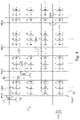
- FIG. 1 is a simplified functional block diagram of a display panel 100 according to one embodiment of the present disclosure.
- the display panel 100 comprises a scan driver circuit 110 , a plurality of pixel circuits 120 , a plurality of gate lines GL, a plurality of data lines SL, a plurality of control lines EL, a plurality of first clock lines CLa, and a plurality of second clock lines CLb.
- the first clock lines CLa are configured to correspondingly transmit a plurality of first clock signals CK 1 -CK 4 .
- the second clock lines CLb are configured to correspondingly transmit a plurality of second clock signals HC 1 -HC 8 .
- the pixel circuits 120 are disposed in an active area AA of the display panel 100 , and are arranged correspondingly near intersections of the gate lines GL and the data lines SL.
- the display panel 100 provides data signals to the data lines SL to specify a gray value (brightness) for each pixel circuit 120 , and a time point of each pixel circuit 120 to receive the data signal are determined by a signal on a corresponding gate line GL.
- the active area AA is an area which the pixel circuits 120 are arranged as an array to display pictures.
- the scan driver circuit 110 comprises a plurality of stages of shift register unit 1121 - 112 n and a plurality of gate control circuits 114 .
- the shift register units 1121 - 112 n are arranged in the peripheral area PA of the display panel 100 , in which the peripheral area PA surrounds the active area AA.
- the gate control circuits 114 are arranged in the active area AA, in which each gate control circuit 114 is arranged near an intersection of a corresponding second clock line CLb and a corresponding control line EL.
- shift register unit 112 will be used to refer to any non-specific one among the shift register units 1121 - 112 n.
- Each stage of shift register unit 112 is configured to receive a corresponding one of the first clock signals CK 1 -CK 4 from the first clock line CLa.
- Each stage of shift register unit 112 is further coupled with corresponding four control lines EL, and is coupled with a corresponding gate control circuit 114 through each control line EL, but this disclosure is not limited thereto.
- Each gate control circuit 114 is configured to receive a corresponding one of the second clock signals HC 1 -HC 8 from the second clock line CLb, and is coupled with a corresponding row of pixel circuit 120 through the gate line GL.
- the shift register unit 112 and the gate control circuits 114 coupled together are configured to cooperatively drive multiple corresponding rows of pixel circuit 120 .
- each stage of shift register unit 112 may be coupled with the control lines EL of a non-specific number, and may be coupled with gate control circuits 114 of a non-specific number through each control line EL.
- the shift register unit 112 may be coupled with eight control lines EL, and may be coupled with two or more than two gate control circuits 114 through each control line EL to increase driving ability.
- Any two gate control circuits 114 coupled with the same stage of shift register unit 112 and with the same control line EL, are coupled with the same gate line GL and receive the same one of the second clock signals HC 1 -HC 8 .
- any two gate control circuits 114 coupled with the same stage of shift register unit 112 but with different gate lines GL, receive different two of the second clock signals HC 1 -HC 8 .
- pixel circuit 120 Although only one column of pixel circuit 120 is arranged between two adjacent second clock lines CLb in the embodiment of FIG. 1 , multiple columns of pixel circuit 120 may be arranged between two adjacent second clock lines CLb in practice, so as to distribute the gate control circuits 114 evenly in the active area AA.
- FIG. 2 is an enlarged view of a portion of the display panel 100 according to one embodiment of the present disclosure.
- each gate control circuit 114 comprises a first transistor T 1 and a second transistor T 2 , in which each of the first transistor T 1 and the second transistor T 2 comprises a first terminal, a second terminal, and a control terminal.
- the first terminal of the first transistor T 1 is configured to receive a corresponding one of the second clock signals HC 1 -HC 8 .
- the second terminal of the first transistor T 1 is coupled with a corresponding gate line GL, and is configured to provide a corresponding one of multiple gate signals GP 1 -GP 4 .
- the control terminal of the first transistor T 1 is coupled with a corresponding shift register unit 112 through a corresponding control line EL.
- the pixel circuit 120 comprises three sub-pixel circuits configured to provide red light, green light, and blue light, but this disclosure is not limited thereto. In practice, the number and color of sub-pixels in the pixel circuit 120 may be designed based on practical requirements.
- the gate control circuits 114 of FIG. 2 are coupled with the same shift register unit 112 , and are configured to receive the same control signal CT from that same shift register unit 112 through the control lines EL.
- FIG. 3 is a waveform schematic of the control signal CT and the gate signals GP 1 -GP 4 according to one embodiment of the present disclosure. Reference is made to FIG. 2 and FIG. 3 .
- the control signal CT has a logic high level
- the first transistor T 1 is conducted to output a corresponding one of the second clock signals HC 1 -HC 8 as a corresponding one of the gate signals GP 1 -GP 4 to the gate line GL, and the second transistor T 2 is switched off.
- the second clock signals HC 1 -HC 8 sequentially provide pulses as will be illustrated in the following FIG. 6 . Therefore, the gate signals GP 1 -GP 4 sequentially switch to the logic high level, and then sequentially switch to a logic low level, so as to sequentially drive multiple rows of pixel circuit 120 as shown in FIG. 2 .
- the highest voltage (or amplitude) of the control signal CT is set to be higher than the highest voltage (or amplitude) of each of the second clock signals HC 1 -HC 8 .
- a pulse width of the control signal CT is greater than a pulse width of each of the second clock signals HC 1 -HC 8 (or each of the gate signals GP 1 -GP 4 ).
- the first transistor T 1 and the second transistor T 2 are switched off. In this situation, if the first transistor T 1 is conducted accidentally due to oscillation of the second clock signals HC 1 -HC 8 , the second transistor T 2 forms a diode-connected transistor to stabilize the gate line GL at approximate the logic low level of the control signal CT.
- FIG. 4 is an enlarged view of a portion of the display panel 100 according to another embodiment of the present disclosure.
- the gate control circuit 114 of FIG. 4 is similar to the gate control circuit 114 of FIG. 2 , one of the differences is that the control terminal of the second transistor T 2 of the gate control circuit 114 in FIG. 4 is coupled with the first terminal of the first transistor T 1 .
- FIG. 5 is a circuit schematic of a shift register unit 500 according to one embodiment of the present disclosure.
- the shift register unit 500 comprises an output node NO[i], a driving node NQ, a voltage stabilization node NP, a third transistor T 3 , a fourth transistor T 4 , a voltage input circuit 510 , and a voltage stabilization circuit 520 .
- the output node NO[i] is configured to provide the control signal CT, and is coupled with multiple corresponding control lines EL.
- the output node NO[i] is further coupled, through each control line EL, with one or more corresponding gate control circuits 114 .
- the output node NO[i] may be coupled with all of the control lines EL in FIG. 2 .
- Each of the third transistor T 3 and the fourth transistor T 4 comprises a first terminal, a second terminal, and a control terminal.
- the first terminal of the third transistor T 3 is configured to receive a corresponding one of the first clock signals CK 1 -CK 4 (e.g., the first clock signal CK 1 ).
- the second terminal of the third transistor T 3 is coupled with the output node NO[i].
- the control terminal of the third transistor T 3 is coupled with the driving node NQ. That is, the third transistor T 3 is configured to provide the corresponding one of the first clock signals CK 1 -CK 4 to the output node NO[i] as the control signal CT.
- the first terminal of the fourth transistor T 4 is coupled with the driving node NO.
- the second terminal of the fourth transistor T 4 is configured to receive the first reference voltage VSSQ.
- the control terminal of the fourth transistor T 4 is coupled with an output node NO[i+2] of a post-two stage shift register unit 112 among the shift register units 1121 - 112 n.
- the voltage input circuit 510 is configured to set the driving node NQ and the voltage stabilization node NP to the first reference voltage VSSQ or to set the driving node NQ to a second reference voltage VGHD, according to a voltage of an output node NO[i ⁇ 2] of a previous-two stage shift register unit 112 among the shift register units 1121 - 112 n and also according to the start signal ST.
- the voltage input circuit 510 comprises a fifth transistor T 5 , a sixth transistor T 6 , and a seventh transistor T 7 , in which each of the fifth transistor T 5 , the sixth transistor T 6 , and the seventh transistor T 7 comprises a first terminal, a second terminal, and a control terminal.
- the first terminal of the fifth transistor T 5 is configured to receive the second reference voltage VGHD.
- the second terminal of the fifth transistor T 5 is coupled with the driving node NQ.
- the control terminal of the fifth transistor T 5 is coupled with the output node NO[i ⁇ 2] of the previous-two stage shift register unit 112 .
- the first terminal of the sixth transistor T 6 is coupled with the driving node NQ.
- the second terminal of the sixth transistor T 6 is configured to receive the first reference voltage VSSQ.
- the control terminal of the sixth transistor T 6 is configured to receive the start signal ST.
- the first terminal of the seventh transistor T 7 is coupled with the voltage stabilization node NP.
- the second terminal of the seventh transistor T 7 is configured to receive the first reference voltage VSSQ.
- the control terminal of the seventh transistor T 7 is configured to receive the start signal ST.
- the start signal ST may provide a pulse when each frame is started to conduct the sixth transistor T 6 and the seventh transistor T 7 , so as to reset voltages of the driving node NQ and the voltage stabilization node NP.
- the voltage stabilization circuit 520 is configured to stabilize voltages of the driving node NQ and the output node NO[i], according to a corresponding one of the first clock signals CK 1 -CK 4 (e.g., the first clock signal CK 1 ) and a voltage of the voltage stabilization node NP.
- the voltage stabilization circuit 520 comprises an eighth transistor T 8 , a ninth transistor T 9 , a tenth transistor T 10 , and a capacitor Cs, in which each of the eighth transistor T 8 , the ninth transistor T 9 , and the tenth transistor T 10 comprises a first terminal, a second terminal, and a control terminal.
- the first terminal of the eighth transistor T 8 is coupled with the output node NO[i].
- the second terminal of the eighth transistor T 8 is configured to receive the third reference voltage VSSG.
- the control terminal of the eighth transistor T 8 is coupled with the voltage stabilization node NP.
- the first terminal of the ninth transistor T 9 is coupled with the driving node NQ.
- the second terminal of the ninth transistor T 9 is configured to receive the first reference voltage VSSQ.
- the control terminal of the ninth transistor T 9 is coupled with the voltage stabilization node NP.
- the first terminal of the tenth transistor T 10 is coupled with the voltage stabilization node NP.
- the second terminal of the tenth transistor T 10 is configured to receive the first reference voltage VSSQ.
- the control terminal of the tenth transistor T 10 is coupled with the driving node NQ.
- the capacitor Cs comprises a first terminal and a second terminal.
- the first terminal of the capacitor Cs is configured receive a corresponding one of the first clock signals CK 1 -CK 4 (e.g., the first clock signal CK 1 ).
- the second terminal of the capacitor Cs is coupled with the voltage stabilization node NP.
- the clock signal received by the first terminal of the capacitor Cs is in phase with the clock signal received by the first terminal of the third transistor T 3 , but the first terminal of the capacitor Cs and the first terminal of the third transistor T 3 need not to receive the same clock signal and may receive different clock signals.
- FIG. 6 is a waveform schematic of the first clock signals CK 1 -CK 4 and the second clock signals HC 1 -HC 8 according to one embodiment of the present disclosure. Reference is made to FIG. 1 and FIG. 6 .
- the shift register unit 112 When the corresponding one of the first clock signals CK 1 -CK 4 received by the shift register unit 112 has the logic high level, the shift register unit 112 outputs the control signal CT having the logic high level.
- the shift register unit 112 outputs the control signal CT having the logic low level.
- the shift register unit 1121 of FIG. 1 outputs the control signal CT having the logic high level when the first clock signal CK 1 has the logic high level.
- the gate control circuit 114 coupled with the shift register unit 1121 provides the second clock signals HC 3 -HC 6 as the gate signals GP 1 -GP 4 , respectively, to sequentially drive multiple corresponding rows of pixel circuit 120 .
- the shift register unit 1122 of FIG. 1 outputs control signal CT having the logic high level when the first clock signal CK 2 has the logic high level.
- the gate control circuit 114 coupled with the shift register unit 1122 provides the second clock signals HC 7 -HC 8 and HC 1 -HC 2 as the gate signals GP 1 -GP 4 , respectively, to sequentially drive multiple corresponding rows of pixel circuit 120 , and so forth.
- the highest voltage (or amplitude) of each of the first clock signals CK 1 -CK 4 is higher than the highest voltage (or amplitude) of each of the second clock signals HC 1 -HC 8 .
- a pulse width of each of the first clock signals CK 1 -CK 4 is greater than a pulse width of each of the second clock signals HC 1 -HC 8 .
- the second clock signals HC 1 -HC 8 provide pulses of a number larger than or equal to M.
- the second clock signals HC 1 -HC 8 provide pulses of a number equal to eight.
- the transistors of the shift register unit 112 and the gate control circuit 114 may be implemented by various suitable N-type transistors.
- the thin-film transistor (TFT), MOSFETs, or bipolar junction transistors may be implemented by various suitable N-type transistors.
- TFT thin-film transistor
- MOSFETs MOSFETs
- bipolar junction transistors bipolar junction transistors
- the transistors of the shift register unit 112 and the gate control circuit 114 may be implemented by various P-type transistors.
- the first clock signals CK 1 -CK 4 and the second clock signals HC 1 -HC 8 may have waveforms opposite to that depicted in FIG. 6 .
- each stage of the shift register unit 112 in this disclosure can simultaneously drive multiple rows of pixel circuit 120 , different from the conventional shift register unit that can drive only one row of pixel circuit. Therefore, the display panel 100 needs few shift register units 112 , helping to reduce width of the display border.
- the positions at which the gate control circuits 114 are arranged on the gate lines GL may be adjusted freely to render the gate control circuits 114 be evenly distributed in the active area AA. Therefore, signals in the display panel 100 transmitted on the gate lines GL have low transmission delay.
Landscapes
- Engineering & Computer Science (AREA)
- Physics & Mathematics (AREA)
- Computer Hardware Design (AREA)
- General Physics & Mathematics (AREA)
- Theoretical Computer Science (AREA)
- Control Of Indicators Other Than Cathode Ray Tubes (AREA)
Abstract
Description
Claims (17)
Applications Claiming Priority (2)
| Application Number | Priority Date | Filing Date | Title |
|---|---|---|---|
| TW109102501A TWI717983B (en) | 2020-01-22 | 2020-01-22 | Display panel and shift register thereof suitable for narrow border application |
| TW109102501 | 2020-01-22 |
Publications (2)
| Publication Number | Publication Date |
|---|---|
| US20210225240A1 US20210225240A1 (en) | 2021-07-22 |
| US11475813B2 true US11475813B2 (en) | 2022-10-18 |
Family
ID=74979385
Family Applications (1)
| Application Number | Title | Priority Date | Filing Date |
|---|---|---|---|
| US17/067,795 Active 2041-02-19 US11475813B2 (en) | 2020-01-22 | 2020-10-12 | Display panel and scan driver circuit thereof suitable for narrow border application |
Country Status (3)
| Country | Link |
|---|---|
| US (1) | US11475813B2 (en) |
| CN (1) | CN112530339B (en) |
| TW (1) | TWI717983B (en) |
Families Citing this family (1)
| Publication number | Priority date | Publication date | Assignee | Title |
|---|---|---|---|---|
| TWI763235B (en) | 2021-01-06 | 2022-05-01 | 友達光電股份有限公司 | Display panel |
Citations (10)
| Publication number | Priority date | Publication date | Assignee | Title |
|---|---|---|---|---|
| US20070229433A1 (en) * | 2006-03-30 | 2007-10-04 | Lg. Philips Lcd Co. Ltd. | Display device and driving method thereof |
| US20090041177A1 (en) * | 2007-08-07 | 2009-02-12 | Au Optronics Corp. | Shift register arrays |
| US20120212275A1 (en) * | 2011-02-22 | 2012-08-23 | Yong-Ho Jang | Gate Driving Circuit |
| US8422620B2 (en) | 2009-07-01 | 2013-04-16 | Au Optronics Corp. | Shift registers |
| US20130222357A1 (en) | 2012-02-23 | 2013-08-29 | Chien-Chang Tseng | Gate driver for liquid crystal display |
| CN103280198A (en) | 2013-02-06 | 2013-09-04 | 友达光电股份有限公司 | Display panel and gate driver thereof |
| US20150235590A1 (en) | 2014-02-17 | 2015-08-20 | Au Optronics (Xiamen) Corporation | Display panel and gate driver |
| US20160358666A1 (en) * | 2015-06-08 | 2016-12-08 | Boe Technology Group Co., Ltd. | Shift register unit, gate driving circuit and driving method thereof, and array substrate |
| US20170047030A1 (en) * | 2015-08-12 | 2017-02-16 | Samsung Display Co., Ltd. | Display device |
| US20170178558A1 (en) * | 2015-06-24 | 2017-06-22 | Boe Technology Group Co., Ltd. | Shift register unit and method for driving the same, gate drive circuit and display device |
Family Cites Families (8)
| Publication number | Priority date | Publication date | Assignee | Title |
|---|---|---|---|---|
| US7738050B2 (en) * | 2007-07-06 | 2010-06-15 | Semiconductor Energy Laboratory Co., Ltd | Liquid crystal display device |
| US9734757B2 (en) * | 2012-10-17 | 2017-08-15 | Joled Inc. | Gate driver integrated circuit, and image display apparatus including the same |
| CN102983132B (en) * | 2012-11-29 | 2015-04-22 | 京东方科技集团股份有限公司 | Array substrate and display device |
| TWI679624B (en) * | 2014-05-02 | 2019-12-11 | 日商半導體能源研究所股份有限公司 | Semiconductor device |
| TWM498327U (en) * | 2014-11-19 | 2015-04-01 | Giantplus Technology Co Ltd | Display gate drive circuit structure |
| TW201624447A (en) * | 2014-12-30 | 2016-07-01 | 中華映管股份有限公司 | Display panel |
| WO2018073690A1 (en) * | 2016-10-21 | 2018-04-26 | Semiconductor Energy Laboratory Co., Ltd. | Touch sensor, display device, display module, and electronic device |
| KR20250024112A (en) * | 2017-02-17 | 2025-02-18 | 가부시키가이샤 한도오따이 에네루기 켄큐쇼 | Display device |
-
2020
- 2020-01-22 TW TW109102501A patent/TWI717983B/en active
- 2020-10-12 US US17/067,795 patent/US11475813B2/en active Active
- 2020-11-02 CN CN202011204618.1A patent/CN112530339B/en active Active
Patent Citations (11)
| Publication number | Priority date | Publication date | Assignee | Title |
|---|---|---|---|---|
| US20070229433A1 (en) * | 2006-03-30 | 2007-10-04 | Lg. Philips Lcd Co. Ltd. | Display device and driving method thereof |
| US20090041177A1 (en) * | 2007-08-07 | 2009-02-12 | Au Optronics Corp. | Shift register arrays |
| US8422620B2 (en) | 2009-07-01 | 2013-04-16 | Au Optronics Corp. | Shift registers |
| US20120212275A1 (en) * | 2011-02-22 | 2012-08-23 | Yong-Ho Jang | Gate Driving Circuit |
| US20130222357A1 (en) | 2012-02-23 | 2013-08-29 | Chien-Chang Tseng | Gate driver for liquid crystal display |
| US9030399B2 (en) | 2012-02-23 | 2015-05-12 | Au Optronics Corporation | Gate driver stage outputting multiple, partially overlapping gate-line signals to a liquid crystal display |
| CN103280198A (en) | 2013-02-06 | 2013-09-04 | 友达光电股份有限公司 | Display panel and gate driver thereof |
| US20150235590A1 (en) | 2014-02-17 | 2015-08-20 | Au Optronics (Xiamen) Corporation | Display panel and gate driver |
| US20160358666A1 (en) * | 2015-06-08 | 2016-12-08 | Boe Technology Group Co., Ltd. | Shift register unit, gate driving circuit and driving method thereof, and array substrate |
| US20170178558A1 (en) * | 2015-06-24 | 2017-06-22 | Boe Technology Group Co., Ltd. | Shift register unit and method for driving the same, gate drive circuit and display device |
| US20170047030A1 (en) * | 2015-08-12 | 2017-02-16 | Samsung Display Co., Ltd. | Display device |
Non-Patent Citations (1)
| Title |
|---|
| ManHong Na et al., 4-side Micro Border 8k4k LCD with Oxide-TFT Gate Driver Embedded Array, Published Mar. 1, 2020, AU Optronics Corp. |
Also Published As
| Publication number | Publication date |
|---|---|
| US20210225240A1 (en) | 2021-07-22 |
| CN112530339B (en) | 2023-08-11 |
| TWI717983B (en) | 2021-02-01 |
| TW202129619A (en) | 2021-08-01 |
| CN112530339A (en) | 2021-03-19 |
Similar Documents
| Publication | Publication Date | Title |
|---|---|---|
| US11837147B2 (en) | Display substrate, display panel, display apparatus and display driving method | |
| US10943552B2 (en) | Shift register unit, gate drive circuit and method of driving the same | |
| US10540938B2 (en) | Shift-buffer circuit, gate driving circuit, display panel and driving method | |
| US20170178581A1 (en) | Shift register, gate driving circuit, method for driving display panel and display device | |
| US11600224B2 (en) | Gate driving circuit and driving method thereof, display panel | |
| US11056064B2 (en) | Electronic device capable of reducing peripheral circuit area | |
| CN115064111B (en) | Drive control circuit, control method thereof and display device | |
| US20180218660A1 (en) | Shift register, gate driving circuit and display apparatus | |
| US20130257703A1 (en) | Image display systems and bi-directional shift register circuits | |
| US20200027404A1 (en) | Display panel, method for driving the same, and display device | |
| CN116631325A (en) | Display panel, driving method thereof, and display device | |
| US20160104449A1 (en) | Display panel and bi-directional shift register circuit | |
| US20160275849A1 (en) | Display devices | |
| US11386863B2 (en) | Output circuit of driver | |
| US20190180666A1 (en) | Shift register, gate driving circuit, display device, and gate driving method | |
| KR20200020328A (en) | Organic Light Emitting Diode display panel and Organic Light Emitting Diode display device using the same | |
| KR20190036447A (en) | Display panel and Organic Light Emitting Diode display device using the same | |
| US11475813B2 (en) | Display panel and scan driver circuit thereof suitable for narrow border application | |
| US10998069B2 (en) | Shift register and electronic device having the same | |
| US10984709B2 (en) | Display panel | |
| US11462174B2 (en) | Plurality of scan driver having shared scan lines and display apparatus including the same | |
| TWI740596B (en) | Shift register and electronic apparatus having the same | |
| CN118379963B (en) | Gate driving circuit and display panel | |
| US20250182701A1 (en) | Driving signal output circuit, screen driving circuit, display screen, and electronic device | |
| KR102581724B1 (en) | Display Device |
Legal Events
| Date | Code | Title | Description |
|---|---|---|---|
| AS | Assignment |
Owner name: AU OPTRONICS CORPORATION, TAIWAN Free format text: ASSIGNMENT OF ASSIGNORS INTEREST;ASSIGNORS:TUNG, CHE-WEI;LIN, WEI-LI;LIN, YU-ZUO;AND OTHERS;SIGNING DATES FROM 20201006 TO 20201007;REEL/FRAME:054023/0202 |
|
| FEPP | Fee payment procedure |
Free format text: ENTITY STATUS SET TO UNDISCOUNTED (ORIGINAL EVENT CODE: BIG.); ENTITY STATUS OF PATENT OWNER: LARGE ENTITY |
|
| STPP | Information on status: patent application and granting procedure in general |
Free format text: DOCKETED NEW CASE - READY FOR EXAMINATION |
|
| STPP | Information on status: patent application and granting procedure in general |
Free format text: NON FINAL ACTION MAILED |
|
| STPP | Information on status: patent application and granting procedure in general |
Free format text: RESPONSE TO NON-FINAL OFFICE ACTION ENTERED AND FORWARDED TO EXAMINER |
|
| STPP | Information on status: patent application and granting procedure in general |
Free format text: NOTICE OF ALLOWANCE MAILED -- APPLICATION RECEIVED IN OFFICE OF PUBLICATIONS |
|
| STPP | Information on status: patent application and granting procedure in general |
Free format text: PUBLICATIONS -- ISSUE FEE PAYMENT RECEIVED |
|
| STPP | Information on status: patent application and granting procedure in general |
Free format text: PUBLICATIONS -- ISSUE FEE PAYMENT VERIFIED |
|
| STCF | Information on status: patent grant |
Free format text: PATENTED CASE |
|
| MAFP | Maintenance fee payment |
Free format text: PAYMENT OF MAINTENANCE FEE, 4TH YEAR, LARGE ENTITY (ORIGINAL EVENT CODE: M1551); ENTITY STATUS OF PATENT OWNER: LARGE ENTITY Year of fee payment: 4 |