US11468307B2 - Artificial neuromorphic circuit and operation method - Google Patents
Artificial neuromorphic circuit and operation method Download PDFInfo
- Publication number
- US11468307B2 US11468307B2 US16/955,026 US201916955026A US11468307B2 US 11468307 B2 US11468307 B2 US 11468307B2 US 201916955026 A US201916955026 A US 201916955026A US 11468307 B2 US11468307 B2 US 11468307B2
- Authority
- US
- United States
- Prior art keywords
- circuit
- signal
- post
- neuron
- control signal
- Prior art date
- Legal status (The legal status is an assumption and is not a legal conclusion. Google has not performed a legal analysis and makes no representation as to the accuracy of the status listed.)
- Active, expires
Links
Images


Classifications
-
- G—PHYSICS
- G06—COMPUTING OR CALCULATING; COUNTING
- G06N—COMPUTING ARRANGEMENTS BASED ON SPECIFIC COMPUTATIONAL MODELS
- G06N3/00—Computing arrangements based on biological models
- G06N3/02—Neural networks
- G06N3/06—Physical realisation, i.e. hardware implementation of neural networks, neurons or parts of neurons
- G06N3/063—Physical realisation, i.e. hardware implementation of neural networks, neurons or parts of neurons using electronic means
-
- G—PHYSICS
- G06—COMPUTING OR CALCULATING; COUNTING
- G06N—COMPUTING ARRANGEMENTS BASED ON SPECIFIC COMPUTATIONAL MODELS
- G06N3/00—Computing arrangements based on biological models
- G06N3/02—Neural networks
- G06N3/04—Architecture, e.g. interconnection topology
- G06N3/049—Temporal neural networks, e.g. delay elements, oscillating neurons or pulsed inputs
-
- G—PHYSICS
- G06—COMPUTING OR CALCULATING; COUNTING
- G06N—COMPUTING ARRANGEMENTS BASED ON SPECIFIC COMPUTATIONAL MODELS
- G06N3/00—Computing arrangements based on biological models
- G06N3/02—Neural networks
- G06N3/06—Physical realisation, i.e. hardware implementation of neural networks, neurons or parts of neurons
- G06N3/063—Physical realisation, i.e. hardware implementation of neural networks, neurons or parts of neurons using electronic means
- G06N3/065—Analogue means
-
- G—PHYSICS
- G06—COMPUTING OR CALCULATING; COUNTING
- G06N—COMPUTING ARRANGEMENTS BASED ON SPECIFIC COMPUTATIONAL MODELS
- G06N3/00—Computing arrangements based on biological models
- G06N3/02—Neural networks
- G06N3/08—Learning methods
- G06N3/088—Non-supervised learning, e.g. competitive learning
Definitions
- the present disclosure relates to a circuit technology. More particularly, the present disclosure relates to an artificial neuromorphic circuit and an operation method.
- a living body has a neural network system.
- the neural network system contains many neurons. Neurons were proposed by Heinrich Wilhelm Gottfried von Waldeyer-Hartz in 1891. Neurons are processing units that obtain discrete information from the brain. In 1897, Charles Sherrington called the junction between two neurons a “synapse.” The discrete information from the brain flows through the synapse along one direction, and the neurons are divided into a “presynaptic neuron” and a “postsynaptic neuron” according to this direction. A neuron emits a “spike” when receiving enough input and being activated.
- the captured experience is translated into synaptic conductance in the brain.
- the synaptic conductance changes over time based on the relative spike times of the presynaptic neuron circuit and the postsynaptic neuron. If the postsynaptic neuron fires before the presynaptic neuron circuit fires, the synaptic conductance will increase. If the two fire in reverse order, the synaptic conductance will decrease. In addition, this change depends on the delay between the two events. The longer the delay, the smaller the change is.
- An artificial neural network allows an electronic system to operate in a manner similar to a biological brain.
- a neuron system may include various electronic circuits that model biological neurons.
- a neural network system affects the perception, selection, decision, or various other behaviors of the living body, so the neural network system plays a very important role in the living body. If circuits can be utilized to build neural network systems similar to those in the living bodies, they will have key influences on many areas.
- the artificial neuromorphic circuit comprises a synapse circuit and a post-neuron circuit.
- the synapse circuit comprises a phase change element, a first switch, and a second switch.
- the first switch is coupled to the phase change element, and is configured to receive a first pulse signal.
- the second switch is coupled to the phase change element, and is configured to receive a second pulse signal.
- the post-neuron circuit comprises an input terminal, a switch circuit, a capacitor, and an output terminal.
- the input terminal is coupled to the phase change element.
- the switch circuit is coupled to the input terminal.
- the capacitor is coupled to the switch circuit. The input terminal charges the capacitor through the switch circuit in response to the first pulse signal.
- the post-neuron circuit generates a firing signal at the output terminal based on a voltage level of the capacitor and a threshold voltage, and generates a first control signal and a second control signal based on the firing signal.
- the first control signal is configured to turn off the switch circuit
- the second control signal is configured to cooperate with the second pulse signal to control the second switch so as to control a state of the phase change element.
- the artificial neuromorphic circuit further comprises a pre-neuron circuit.
- the pre-neuron circuit is coupled to the synapse circuit, and is configured to send the first pulse signal and the second pulse signal.
- the post-neuron circuit further comprises a comparator.
- the comparator is configured to compare the voltage level of the capacitor and the threshold voltage to generate the firing signal.
- the post-neuron circuit further comprises a first controller and a second controller.
- the first controller is coupled to the output terminal and a control terminal of the switch circuit.
- the first controller generates the first control signal to the control terminal according to the firing signal.
- the second controller is coupled to the output terminal and the input terminal. The second controller generates the second control signal based on the firing signal.
- the switch circuit comprises a transistor.
- the first controller comprises a high pass filter.
- the high pass filter generates the first control signal after filtering the firing signal to turn off the transistor.
- the second controller comprises a delay circuit and a pulse generator.
- the delay circuit is coupled to the output terminal and is configured to delay the firing signal.
- the pulse generator is coupled to the delay circuit and is configured to generate the second control signal according to the delayed firing signal.
- the pulse generator transmits the second control signal to the phase change element.
- the present disclosure provides an operation method of an artificial neuromorphic circuit.
- the operation method comprises: receiving a first pulse signal by using a first switch of a synapse circuit; charging an input terminal of a post-neuron circuit through a switch circuit in response to the first pulse signal; using a comparator unit to compare a voltage level of the input terminal and a threshold voltage to generate a firing signal by the post-neuron circuit; generating a first control signal and a second control signal based on the firing signal by using the post-neuron circuit; turning off the switch circuit according to the first control signal by using the post-neuron circuit; and cooperatively controlling a second switch of the synapse circuit based on the second control signal and a second pulse signal to adjust a magnitude of a current flowing through a phase change element of the synapse circuit so as to determined a weight of the artificial neuromorphic circuit.
- the step of turning off the switch circuit according to the first control signal by using the post-neuron circuit comprises: generating the first control signal to turn off the switch circuit according to the firing single by using a controller of the post-neuron circuit, wherein the controller is coupled to an output terminal of the post-neuron circuit and the switch circuit.
- the switch circuit comprises a transistor.
- the controller comprises a filter.
- the step of generating the first control signal to turn off the switch circuit according to the firing single by using the controller of the post-neuron circuit comprises: generating the first control signal after filtering the firing signal by using the filter to turn off the transistor.
- the filter comprises a high pass filter.
- the step of generating the first control signal after filtering the firing signal by using the filter to turn off the transistor comprises: generating the first control signal after filtering the firing signal by using the high pass filter to turn off the transistor.
- the operation method further comprises: delaying the firing signal by using a delay circuit of the post-neuron circuit; generating the second control signal according to the delayed firing signal by using a pulse generator of the post-neuron circuit; and transmitting the second control signal to the phase change element by using the pulse generator.
- the artificial neuromorphic circuit and operation method of the present disclosure can utilize circuits to build an artificial neural network system.
- FIG. 1 depicts a schematic diagram of an artificial neuromorphic circuit according to some embodiments of the present disclosure
- FIG. 2 depicts a schematic diagram of an artificial neuromorphic circuit according to some embodiments of the present disclosure
- FIG. 3 depicts a waveform diagram of multiple signals according to some embodiments of the present disclosure
- FIG. 4 depicts a schematic diagram of an artificial neuromorphic circuit according to some embodiments of the present disclosure
- FIG. 5 depicts a schematic diagram of an artificial neuromorphic circuit according to some embodiments of the present disclosure
- FIG. 6 depicts a schematic diagram of an artificial neuromorphic circuit according to some embodiments of the present disclosure
- FIG. 7 depicts a schematic diagram of an artificial neuromorphic circuit according to some embodiments of the present disclosure.
- FIG. 8 depicts a flowchart of an operation method of an artificial neuromorphic circuit according to some embodiments of the present disclosure.
- Coupled may also be termed “electrically coupled,” and the term “connected” may be termed “electrically connected.” “Coupled” and “connected” may also be used to indicate that two or more elements cooperate or interact with each other.
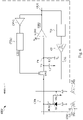
- FIG. 1 and FIG. 2 depict schematic diagrams of an artificial neuromorphic circuit 1000 according to some embodiments of the present disclosure.
- the artificial neuromorphic circuit 1000 includes a synapse circuit 1200 , a pre-synaptic neuron circuit 1300 (hereinafter referred to as “pre-neuron” 1300 ), and a post-synaptic neuron circuit 1400 (hereinafter referred to as “post-neuron” 1400 ).
- the pre-neuron 1300 includes an axon driver 1310 .
- the axon driver 1310 includes two pulse generators G 1 , G 2 .
- the post-neuron 1400 includes dendrites configured to receive a signal.
- the axon driver 1310 of the pre-neuron 1300 sends a spike, which is transmitted to the dendrites of the post-neuron 1400 via the synapse circuit 1200 to stimulate the post-neuron 1400 . In this manner, an effect similar to signal transmission in the neural network system is achieved.
- the synapse circuit 1200 includes a phase change element PCM, a switch D 1 , and a switch SW 2 .
- the phase change element PCM includes a phase change material.
- the phase change material has different phases according to a magnitude of a current. Information can be stored in the phase correspondingly. For example, when the phase change element PCM is in a crystalline phase or a polycrystalline phase, its resistance value is lower. When the phase change element PCM is in an amorphous phase, its resistance value is higher.
- the phase change element PCM can store logic 1 or 0 according to a magnitude of the resistance value of the phase change element PCM.
- the switch D 1 is implemented by using a diode, and the switch SW 2 is implemented by using a transistor. In some other embodiments, the switch D 1 may also be implemented by using a transistor.
- the switch D 1 includes a first terminal and a second terminal. The first terminal is an anode terminal and the second terminal is a cathode terminal. The first terminal of the switch D 1 is coupled to the pulse generator G 1 to receive a pulse signal PS 1 . A control terminal of the switch SW 2 is coupled to the pulse generator G 2 to receive a pulse signal PS 2 .
- the second terminal of the switch D 1 and a second terminal of the switch SW 2 are coupled to a first terminal of the phase change element PCM. A second terminal of the phase change element PCM is coupled to the post-neuron 1400 .
- the post-neuron 1400 includes a switch SW 3 , a capacitor C 1 , a resistor R 1 , a comparator COM, a delay circuit TD, a wave-shaping circuit G 3 , and a controller CTR 1 .
- First terminals of the capacitor C 1 and the resistor R 1 are coupled to a voltage terminal V L .
- the voltage terminal V L may be a low voltage terminal, such as a ground terminal GND.
- the comparator COM includes a positive input terminal, a negative input terminal, and an output terminal.
- a second terminal of the capacitor C 1 and a second terminal of the resistor R 1 are coupled to the positive input terminal of the comparator COM.
- the second terminal of the phase change element PCM is coupled to the positive input terminal of the comparator COM through the switch SW 3 of the post-neuron 1400 .
- the negative input terminal of the comparator COM is configured to receive a threshold voltage V th .
- the output terminal of the comparator COM is coupled to the delay circuit TD and an output terminal OUT.
- the delay circuit TD is coupled to the wave-shaping circuit G 3 .
- the wave-shaping circuit G 3 is coupled to the second terminal of the phase change element PCM.
- the controller CTR 1 is coupled to the output terminal OUT and the switch SW 3 ,
- the capacitor C 1 in the post-neuron 1400 simulates an electrical potential of a neuron membrane.
- Vp also called membrane potential Vp
- the neuron membrane has channels that are of different sizes and can control the passage of the charged ions. The charged ions inside and outside the cell membrane can pass these channels to cause a change of the membrane potential Vp.
- the resistor R 1 simulates the electrical effect of the passage of charged ions back and forth through the channels.
- the membrane potential Vp of the post-synaptic neuron membrane is changed after the pulse signal sent by the axon of the pre-synaptic neuron is received by the dendrites of the post-synaptic neuron.
- the behavioral effect corresponding to the post-neuron 1400 is to charge the capacitor C 1 .
- the post-neuron 1400 will output a firing signal (FIRE) when the membrane potential Vp of the capacitor C 1 exceeds the threshold voltage V th .
- the intensity of the pulse signal is not strong enough, the post-neuron 1400 will not output the firing signal (FIRE) and its increased membrane potential Vp will gradually decrease through a leakage of the resistor R 1 although a voltage on the capacitor C 1 rises but, however, does not exceed the threshold voltage V th .
- the behavior on the neuron is that the post-neuron instantly changes the concentrations of charged ions inside and outside the cell membrane due to the firing signal of the pre-neuron, and then the charged ions are balanced by diffusion through the channels on the cell membrane, so that the membrane potential Vp of the post-neuron membrane returns to equilibrium. Therefore, the electrical behavior of the path that the pre-neuron sends the pulse signal to the capacitor C 1 of the post-neuron is called leaky integration and fire (LIF).
- LIF leaky integration and fire
- the firing signal of each pre-neuron affects the membrane potential Vp of the post-neuron 1400 via the synapse (including the axon of the pre-neuron and the dendrites of the post-neuron).
- different pre-neurons have different magnitudes of effects on the membrane potential Vp of the post-neuron 1400 .
- a magnitude of a synaptic weight (W) between the pre-neuron and the post-neuron is different.
- the magnitude of the change of the synaptic weight ( ⁇ W) is related to the time difference between t pre and t post , and the synaptic weight W is adaptively adjusted according to the value of the time difference. Therefore, the synaptic weight W relates to the index of causality between neurons.
- a characteristic index representing that the synapse changes the weight (W) due to the relative relationship between the pre-neuron firing time and the post-neuron firing time is defined, which is called spike timing dependent plasticity (STDP).
- STDP of the synapse is also indirectly related to LIF because LIF can determine the post-neuron firing time (t post ).
- the STDP of the synapse represents the plasticity of the conductivity of synaptic current.
- the STDP of the synapse represents a magnitude of a synaptic resistance in one embodiment.
- the membrane potential Vp of the capacitor C 1 in the post-neuron 140 gradually moves toward an equilibrium potential (VL) via the resistor R 1 .
- the equilibrium potential (VL) is a ground potential.
- the present disclosure is not limited in this regard.
- the switch SW 3 of the post-neuron 1400 is turned on, the pre-neuron 1300 sends the spike to the post-neuron 1400 , the pulse generator G 1 in the axon driver 1310 sends the pulse signal PS 1 at time t 1 , and a pulse width time is t 1 to t 2 .
- the switch D 1 is turned on and the switch SW 2 is turned off.
- the pulse signal PS 1 is also called “axon pulse LIF”, and a width is 0.1 milliseconds (ms).
- the axon pulse LIF passes the phase change element PCM of the synapse circuit 1200 and charges the second terminal of the capacitor C 1 (the positive input terminal of the comparator COM) through the switch SW 3 , so that the cell membrane potential has the voltage level Vp.
- the membrane potential Vp gradually rises during the time interval T 1 . If the voltage level Vp of the capacitor C 1 is higher than the threshold voltage V th of the negative input terminal of the comparator COM before time t 2 (including the point t 2 ), the output terminal of the comparator COM immediately sends the firing signal FIRE at this time. When the membrane potential Vp is lower than the threshold voltage V th , the comparator COM does not output the firing signal FIRE. Therefore, the magnitude of the resistance value of the phase change element PCM can control the speed of charging the capacitor C 1 .
- the pulse generator G 2 of the axon driver 1310 generates the pulse signal PS 2 .
- the pulse signal PS 2 is also called “axon pulse STDP”.
- a pulse time period T of the axon pulse STDP is 100 ms.
- the axon pulse STDP is divided into two time zones of equal time (T/2) front and latter.
- the pulse in the front time zone (T/2) is instantly increased by a voltage value (not marked), and is then gradually increased.
- the pulse in the latter time zone (T/2) is instantly reduced by a voltage value (not marked), and is then gradually lowered.
- a highest voltage value of the axon pulse STDP in the latter time zone is smaller than a lowest voltage value in the latter time zone.
- the firing signal FIRE sent by the output terminal of the comparator COM passes the controller CTR 1 to immediately generate a control signal CS 1 so as to turn off the switch SW 3 .
- the signal of the synapse circuit 1200 can no longer affect the voltage of the capacitor C 1 in the post-neuron 1400 .
- the firing signal FIRE passes the delay circuit TD and the wave-shaping circuit G 3 to output a control signal CS 2 to the second terminal of the phase change element PCM.
- the delay circuit TD will add a delay time td to the firing signal FIRE. In one embodiment, the delay time td is 50 ms.
- control signal CS 2 is sent to the second terminal of the phase change element PCM at time t 3 .
- a pulse duration of the control signal CS 2 is from time t 3 to time t 4 .
- the above control signal CS 2 is also referred to as a “post-synaptic neuron STDP trigger”, and its pulse duration is 0.1 ms.
- the controller CTR 1 sends the control signal CS 1 to turn off the switch SW 3 and maintain a turn-off state to be longer than (including equal to) the pulse time period T of the axon pulse STDP (PS 2 ).
- the capacitor C 1 starts to discharge through the resistor R 1 , and the membrane potential Vp gradually decreases. During this period T, the post-neuron can no longer receive the signal transmitted from any other synaptic circuit.
- the pulse duration of the control signal CS 2 the current flowing through the phase change element PCM in the synapse circuit 1200 is determined by the cooperative effect of the pulse signal PS 2 (the axon pulse STDP) and the control signal CS 2 (the post-synaptic neuron STDP trigger). In other words, signals of the axon pulse STDP (PS 2 ) and the post-synaptic neuron STDP trigger (CS 2 ) can determine a magnitude of the current flowing through the phase change element PCM.
- the axon pulse STDP controls a gate of the switch SW 2 of the synapse circuit 1200 .
- the axon pulse STDP (PS 2 ) controls a gate of the switch SW 2 of the synapse circuit 1200 .
- T/2 front time zone
- T/2 the axon pulse STDP
- its voltage is higher and a current that can flow through the switch SW 2 is larger.
- T/2 time zone
- the switch D 1 in the synapse circuit 1200 is not turned on.
- the post-synaptic neuron STDP trigger (CS 2 ) only flows through the phase change element PCM and the switch SW 2 , and a voltage level of the axon pulse STDP (PS 2 ) can control a magnitude of the current flowing through the switch SW 2 .
- the firing signal (FIRE) of the post-neuron 1400 is caused by the axon pulse LIF (PS 1 ) of the pre-neuron 1300
- the firing time (t post ) of the post-neuron 1400 is later than the firing time (t pre ) of the pre-neuron 1300 .
- the pulse duration of the post-synaptic neuron STDP trigger (CS 2 ) will fall into the latter time zone (T/2) of the axon pulse STDP (PS 2 ). Therefore, the current that instantly flows through the switch SW 2 is smaller, which means that the current instantly flowing through the phase change element PCM is smaller. As a result, the phase change element PCM has a lower resistance value.
- the synapse circuit 1200 has a better conductivity, so it is called synapse long term potentiation. It indicates that the firing of the post-neuron 1400 is related to the pulse signal PS 1 (the axon pulse LIF) of the pre-neuron 1300 . The firing of the post-neuron 1400 is causally related to the firing of the pre-neuron 1300 . The weight W of the synapse circuit 1200 that is connected between the two neurons is thus raised.
- the firing signal (FIRE) of the post-neuron 1400 is not caused by the axon pulse LIF (PS 1 ) of the pre-neuron 1300 , the firing time (t post ) of the post-neuron 1400 is earlier than the firing time (t pre ) of the pre-neuron 1300 .
- the pulse duration of the post-synaptic neuron STDP trigger (CS 2 ) will fall into the front time zone (T/2) of the axon pulse STDP (PS 2 ). Therefore, the current that instantly flows through the switch SW 2 is larger, which means that the current instantly flowing through the phase change element PCM is larger. As a result, the phase change element PCM has a higher resistance value.
- the synapse circuit 1200 has a poorer conductivity, so it is called synapse long term depression. It indicates that the firing of the post-neuron 1400 is not causally related to the firing of the pre-neuron 1300 . The weight W of the synapse circuit 1200 that is connected between the two neurons is thus reduced.
- the artificial neuromorphic circuit 1000 can utilize the above operations to learn behaviors so as to realize the neural network system similar to that in a living body.
- FIG. 4 depicts a schematic diagram of an artificial neuromorphic circuit 2000 according to some embodiments of the present disclosure.
- the artificial neuromorphic circuit 2000 of FIG. 4 differs from the artificial neuromorphic circuit 1000 of FIG. 1 in that a controller of a post-neuron 2400 of the artificial neuromorphic circuit 2000 is a filter HP and the switch SW 3 is a transistor.
- the filter HP is coupled to the output terminal OUT and a gate of the transistor SW 3 .
- the comparator COM will output the positive firing signal FIRE.
- the filter HP immediately generates the control signal CS 1 after receiving the firing signal FIRE to turn off the transistor SW 3 . Since the connection relationships and operations of the other components of the artificial neuromorphic circuit 2000 are similar to those of the artificial neuromorphic circuit 1000 of FIG. 1 , a description in this regard is not provided.
- FIG. 5 depicts a schematic diagram of an artificial neuromorphic circuit 3000 according to some embodiments of the present disclosure.
- the artificial neuromorphic circuit 3000 of FIG. 5 differs from the artificial neuromorphic circuit 2000 of FIG. 4 in that FIG. 5 shows the filter HP of the post-neuron 2400 of the artificial neuromorphic circuit 3000 in detail.
- the filter HP is a high pass filter.
- the high pass filter HP includes a capacitor C 2 and a resistor R 2 .
- the transistor SW 3 is a PMOS.
- the comparator COM When the membrane potential Vp is higher than the threshold voltage V th , the comparator COM outputs the positive peak firing signal FIRE.
- the high pass filter HP immediately generates the high-level control signal CS 1 after receiving the firing signal FIRE to turn off the PMOS (SW 3 ). It is noted that a duration of a turn-off time of the PMOS (SW 3 ) can be determined by adjusting the time constant ⁇ of the capacitor C 2 and the resistor R 2 of the high pass filter HP. Since the connection relationships and operations of the other components of the artificial neuromorphic circuit 3000 are similar to those of the artificial neuromorphic circuit 1000 of FIG. 1 , a description in this regard is not provided.
- FIG. 6 depicts a schematic diagram of an artificial neuromorphic circuit 4000 according to some embodiments of the present disclosure.
- the artificial neuromorphic circuit 4000 of FIG. 6 differs from the artificial neuromorphic circuit 1000 of FIG. 1 in that a controller of a post-neuron 4400 of the artificial neuromorphic circuit 4000 is a filter HP.
- the artificial neuromorphic circuit 4000 further includes an inverter INV 1 and the switch SW 3 is an NMOS in FIG. 6 .
- the filter HP is coupled to a gate of the NMOS (SW 3 ), and is coupled to the output terminal OUT through the inverter INV 1 .
- the comparator COM will output the high-level firing signal FIRE.
- the inverter INV 1 receives the firing signal FIRE to generate an inverted signal.
- the filter HP immediately generates the low-level control signal CS 1 after receiving the inverted signal to turn off the NMOS (SW 3 ). Since the connection relationships and operations of the other components of the artificial neuromorphic circuit 4000 are similar to those of the artificial neuromorphic circuit 1000 of FIG. 1 , a description in this regard is not provided.
- FIG. 7 depicts a schematic diagram of an artificial neuromorphic circuit 5000 according to some embodiments of the present disclosure.
- the artificial neuromorphic circuit 5000 of FIG. 7 differs from the artificial neuromorphic circuit 1000 of FIG. 1 in that a controller of a post-neuron 5400 of the artificial neuromorphic circuit 5000 can be implemented by a level latch LA and a delay circuit TD 2 .
- a controller of a post-neuron 5400 of the artificial neuromorphic circuit 5000 can be implemented by a level latch LA and a delay circuit TD 2 .
- the level latch LA and the delay circuit TD 2 are configured to control a turn-off time and a turn-on time of the switch SW 3 .
- the level latch LA immediately generates a high voltage to turn off the PMOS (SW 3 ), and the delay circuit TD 2 delays a high voltage signal for a period of time to maintain a turn-off state of the PMOS. Since the connection relationships and operations of the other components of the artificial neuromorphic circuit 7000 are similar to those of the artificial neuromorphic circuit 1000 of FIG. 1 , a description in this regard is not provided.
- FIG. 8 depicts a flowchart of an operation method 8000 of an artificial neuromorphic circuit according to some embodiments of the present disclosure.
- the operation method 8000 includes an operation S 8100 , an operation S 8200 , an operation S 8300 , an operation S 8400 , an operation S 8500 , and an operation S 8600 .
- the operation method 8000 is applied to the artificial neuromorphic circuit 1000 of FIG. 1 , but the present disclosure is not limited in this regard.
- FIG. 1 To facilitate understanding, a discussion is provided with reference to FIG. 1 as follows.
- the switch D 1 of the synapse circuit 1200 is used to receive the pulse signal PS 1 .
- the synapse circuit 1200 plays the role of an axon of a pre-synaptic neuron to send a spike to the post-neuron 1400 .
- a positive input terminal of the post-neuron 1400 (the comparator COM) is charged through the switch SW 3 in response to the pulse signal PS 1 .
- the post-neuron 1400 plays the role of dendrites of a post-synaptic neuron to receive a signal from the synapse circuit 1200 .
- the post-neuron 1400 is used to generate the firing signal FIRE based on the voltage level Vp of the positive input terminal and the threshold voltage V th .
- the comparator COM outputs the firing signal FIRE when the voltage level Vp is higher than the threshold voltage V th .
- the post-neuron 1400 is used to generate the control signal CS 1 and the control signal CS 2 based on the firing signal FIRE.
- the controller CTR 1 of the post-neuron 1400 will generate the control signal CS 1 according to the firing signal FIRE.
- the delay circuit TD of the post-neuron 1400 will add a delay time to the firing signal FIRE to output the control signal CS 2 .
- the post-neuron 1400 is used to turn off the switch SW 3 according to the control signal CS 1 .
- the switch SW 3 will be maintained off for a period of time.
- a duration of a turn-off time of the switch SW 3 can be set depending on practical needs.
- the switch SW 2 of the synapse circuit 1200 is controlled based on the control signal CS 2 and the pulse signal PS 2 to control a state of the phase change element PCM of the synapse circuit 1200 . Accordingly, a weight of the artificial neuromorphic circuit 1000 can be determined according to the state of the phase change element PCM.
- the control signal CS 2 flows through the switch SW 2
- the pulse signal PS 2 controls a magnitude of a current that can flow through the switch SW 2 .
- the phase change element PCM includes a phase change material. Different phases of the phase change material correspond to different resistance values.
- the above description of the operation method 8000 includes exemplary operations, but the operations of the operation method 8000 are not limited to the order shown. The order of the operations of the operation method 8000 may be changed, or the operations may be performed simultaneously, partially simultaneously, or partially omitted under appropriate circumstances, which are all within the spirit and scope of the embodiments of the present disclosure.
- the artificial neuromorphic circuit and operation method of the present disclosure can utilize circuits to build an artificial neural network system.
Landscapes
- Engineering & Computer Science (AREA)
- Physics & Mathematics (AREA)
- Theoretical Computer Science (AREA)
- Health & Medical Sciences (AREA)
- Life Sciences & Earth Sciences (AREA)
- Biomedical Technology (AREA)
- Biophysics (AREA)
- Evolutionary Computation (AREA)
- General Engineering & Computer Science (AREA)
- Data Mining & Analysis (AREA)
- Artificial Intelligence (AREA)
- General Health & Medical Sciences (AREA)
- Molecular Biology (AREA)
- Computing Systems (AREA)
- Computational Linguistics (AREA)
- General Physics & Mathematics (AREA)
- Mathematical Physics (AREA)
- Software Systems (AREA)
- Neurology (AREA)
- Electronic Switches (AREA)
- Semiconductor Memories (AREA)
Abstract
Description
Claims (13)
Applications Claiming Priority (1)
| Application Number | Priority Date | Filing Date | Title |
|---|---|---|---|
| PCT/CN2019/118804 WO2021092901A1 (en) | 2019-11-15 | 2019-11-15 | Neural-like circuit and operation method |
Publications (2)
| Publication Number | Publication Date |
|---|---|
| US20220101107A1 US20220101107A1 (en) | 2022-03-31 |
| US11468307B2 true US11468307B2 (en) | 2022-10-11 |
Family
ID=72261323
Family Applications (1)
| Application Number | Title | Priority Date | Filing Date |
|---|---|---|---|
| US16/955,026 Active 2040-09-07 US11468307B2 (en) | 2019-11-15 | 2019-11-15 | Artificial neuromorphic circuit and operation method |
Country Status (3)
| Country | Link |
|---|---|
| US (1) | US11468307B2 (en) |
| CN (1) | CN111630529B (en) |
| WO (1) | WO2021092901A1 (en) |
Families Citing this family (2)
| Publication number | Priority date | Publication date | Assignee | Title |
|---|---|---|---|---|
| TW202527722A (en) * | 2023-09-06 | 2025-07-01 | 日商索尼半導體解決方案公司 | Signal processing device and method for manufacturing semiconductor device |
| CN117875381B (en) * | 2024-01-12 | 2025-09-26 | 北京大学深圳研究生院 | An electronic synaptic circuit and neural network circuit based on ferroelectric tunnel junction |
Citations (24)
| Publication number | Priority date | Publication date | Assignee | Title |
|---|---|---|---|---|
| US20100299297A1 (en) | 2009-05-21 | 2010-11-25 | International Business Machines Corporation | System for electronic learning synapse with spike-timing dependent plasticity using phase change memory |
| CN102543172A (en) | 2012-02-27 | 2012-07-04 | 北京大学 | Control method applicable to resistance changing memory resistor of nerve cell circuit |
| CN102610274A (en) | 2012-04-06 | 2012-07-25 | 电子科技大学 | Weight adjustment circuit for variable-resistance synapses |
| CN102667826A (en) | 2009-11-18 | 2012-09-12 | 国际商业机器公司 | Area efficient neuromorphic circuits |
| US20150278682A1 (en) | 2014-04-01 | 2015-10-01 | Boise State University | Memory controlled circuit system and apparatus |
| US20160203400A1 (en) | 2015-01-14 | 2016-07-14 | International Business Machines Corporation | Neuromorphic memory circuit |
| US20160350643A1 (en) | 2015-05-26 | 2016-12-01 | International Business Machines Corporation | Neuron peripheral circuits for neuromorphic synaptic memory array based on neuron models |
| US20160371583A1 (en) * | 2015-06-22 | 2016-12-22 | International Business Machines Corporation | Communicating postsynaptic neuron fires to neuromorphic cores |
| CN106447033A (en) | 2016-10-13 | 2017-02-22 | 中国科学院深圳先进技术研究院 | Nerve cell synapse circuit and nerve cell circuit |
| CN106470023A (en) | 2015-08-18 | 2017-03-01 | 华为技术有限公司 | Neurn simulation circuit |
| CN106796669A (en) | 2014-10-30 | 2017-05-31 | 国际商业机器公司 | Neuromorphic cynapse |
| CN106815636A (en) | 2016-12-30 | 2017-06-09 | 华中科技大学 | A kind of neuron circuit based on memristor |
| US20170364793A1 (en) | 2016-06-21 | 2017-12-21 | International Business Machines Corporation | System to duplicate neuromorphic core functionality |
| US20170364801A1 (en) | 2016-06-18 | 2017-12-21 | International Business Machines Corporation | Neuromorphic memory circuit |
| CN107615307A (en) | 2015-06-29 | 2018-01-19 | 国际商业机器公司 | Neuromorphic processing equipment |
| CN108780520A (en) | 2016-03-21 | 2018-11-09 | 国际商业机器公司 | artificial neuron device |
| CN108921290A (en) | 2018-06-29 | 2018-11-30 | 清华大学 | Nerve synapse element circuit, nerve network circuit and information processing system |
| CN109255435A (en) | 2017-07-13 | 2019-01-22 | 爱思开海力士有限公司 | Neuromorphic equipment with multiple cynapse blocks |
| US20190065929A1 (en) | 2017-08-25 | 2019-02-28 | International Business Machines Corporation | Neuromorphic synapses |
| CN109727678A (en) | 2017-10-28 | 2019-05-07 | 徐志强 | Variable neuron, cynapse simulator and simulated substrate neural circuitry |
| US10318861B2 (en) | 2015-06-17 | 2019-06-11 | International Business Machines Corporation | Artificial neuron apparatus |
| US20190228292A1 (en) * | 2018-01-24 | 2019-07-25 | International Business Machines Corporation | Synapse memory |
| CN110188873A (en) | 2019-07-08 | 2019-08-30 | 中国人民解放军陆军工程大学 | Feedforward network topology Digital-analog hybrid neural network circuit |
| US20200202217A1 (en) * | 2018-12-19 | 2020-06-25 | SK Hynix Inc. | Neuromorphic system for performing supervised learning using error backpropagation |
Family Cites Families (2)
| Publication number | Priority date | Publication date | Assignee | Title |
|---|---|---|---|---|
| CN103430186A (en) * | 2012-01-20 | 2013-12-04 | 松下电器产业株式会社 | Learning method for neural network circuit |
| CN103078054B (en) * | 2013-01-04 | 2015-06-03 | 华中科技大学 | Unit, device and method for simulating biological neuron and neuronal synapsis |
-
2019
- 2019-11-15 CN CN201980008014.9A patent/CN111630529B/en active Active
- 2019-11-15 US US16/955,026 patent/US11468307B2/en active Active
- 2019-11-15 WO PCT/CN2019/118804 patent/WO2021092901A1/en not_active Ceased
Patent Citations (28)
| Publication number | Priority date | Publication date | Assignee | Title |
|---|---|---|---|---|
| US20100299297A1 (en) | 2009-05-21 | 2010-11-25 | International Business Machines Corporation | System for electronic learning synapse with spike-timing dependent plasticity using phase change memory |
| CN102667826A (en) | 2009-11-18 | 2012-09-12 | 国际商业机器公司 | Area efficient neuromorphic circuits |
| CN102543172A (en) | 2012-02-27 | 2012-07-04 | 北京大学 | Control method applicable to resistance changing memory resistor of nerve cell circuit |
| CN102610274A (en) | 2012-04-06 | 2012-07-25 | 电子科技大学 | Weight adjustment circuit for variable-resistance synapses |
| US20150278682A1 (en) | 2014-04-01 | 2015-10-01 | Boise State University | Memory controlled circuit system and apparatus |
| CN106796669A (en) | 2014-10-30 | 2017-05-31 | 国际商业机器公司 | Neuromorphic cynapse |
| US20160203400A1 (en) | 2015-01-14 | 2016-07-14 | International Business Machines Corporation | Neuromorphic memory circuit |
| US20160203858A1 (en) | 2015-01-14 | 2016-07-14 | International Business Machines Corporation | Neuromorphic memory circuit |
| US9830981B2 (en) | 2015-01-14 | 2017-11-28 | International Business Machines Corporation | Neuromorphic memory circuit using a leaky integrate and fire (LIF) line to transmit axon LIF pulse and a conductive denrite LIF line |
| CN107111783A (en) | 2015-01-14 | 2017-08-29 | 国际商业机器公司 | Neuron memory circuitry |
| US20160350643A1 (en) | 2015-05-26 | 2016-12-01 | International Business Machines Corporation | Neuron peripheral circuits for neuromorphic synaptic memory array based on neuron models |
| US20160350647A1 (en) | 2015-05-26 | 2016-12-01 | International Business Machines Corporation | Neuron peripheral circuits for neuromorphic synaptic memory array based on neuron models |
| US10318861B2 (en) | 2015-06-17 | 2019-06-11 | International Business Machines Corporation | Artificial neuron apparatus |
| US20160371583A1 (en) * | 2015-06-22 | 2016-12-22 | International Business Machines Corporation | Communicating postsynaptic neuron fires to neuromorphic cores |
| CN107615307A (en) | 2015-06-29 | 2018-01-19 | 国际商业机器公司 | Neuromorphic processing equipment |
| CN106470023A (en) | 2015-08-18 | 2017-03-01 | 华为技术有限公司 | Neurn simulation circuit |
| CN108780520A (en) | 2016-03-21 | 2018-11-09 | 国际商业机器公司 | artificial neuron device |
| US20170364801A1 (en) | 2016-06-18 | 2017-12-21 | International Business Machines Corporation | Neuromorphic memory circuit |
| US20170364793A1 (en) | 2016-06-21 | 2017-12-21 | International Business Machines Corporation | System to duplicate neuromorphic core functionality |
| CN106447033A (en) | 2016-10-13 | 2017-02-22 | 中国科学院深圳先进技术研究院 | Nerve cell synapse circuit and nerve cell circuit |
| CN106815636A (en) | 2016-12-30 | 2017-06-09 | 华中科技大学 | A kind of neuron circuit based on memristor |
| CN109255435A (en) | 2017-07-13 | 2019-01-22 | 爱思开海力士有限公司 | Neuromorphic equipment with multiple cynapse blocks |
| US20190065929A1 (en) | 2017-08-25 | 2019-02-28 | International Business Machines Corporation | Neuromorphic synapses |
| CN109727678A (en) | 2017-10-28 | 2019-05-07 | 徐志强 | Variable neuron, cynapse simulator and simulated substrate neural circuitry |
| US20190228292A1 (en) * | 2018-01-24 | 2019-07-25 | International Business Machines Corporation | Synapse memory |
| CN108921290A (en) | 2018-06-29 | 2018-11-30 | 清华大学 | Nerve synapse element circuit, nerve network circuit and information processing system |
| US20200202217A1 (en) * | 2018-12-19 | 2020-06-25 | SK Hynix Inc. | Neuromorphic system for performing supervised learning using error backpropagation |
| CN110188873A (en) | 2019-07-08 | 2019-08-30 | 中国人民解放军陆军工程大学 | Feedforward network topology Digital-analog hybrid neural network circuit |
Non-Patent Citations (2)
| Title |
|---|
| Chung H. Lam, "Neuromorphic Semiconductor Memory", IEEE 2015 International 3D Systems Integration Conference. |
| S. Kim et al., "NVM Neuromorphic Core with 64k-cell (256-by-256) Phase Change Memory Synaptic Array with On-Chip Neuron Circuits for Continuous In-Situ Learning", 2015 IEEE International Electron Devices Meeting (IEDM), 4 pages. |
Also Published As
| Publication number | Publication date |
|---|---|
| CN111630529A (en) | 2020-09-04 |
| WO2021092901A1 (en) | 2021-05-20 |
| US20220101107A1 (en) | 2022-03-31 |
| CN111630529B (en) | 2023-09-01 |
Similar Documents
| Publication | Publication Date | Title |
|---|---|---|
| US11580370B2 (en) | Artificial neuromorphic circuit and operation method | |
| US11551070B2 (en) | Artificial neuromorphic circuit and operation method | |
| KR102230784B1 (en) | Synapse circuit for spike-timing dependent plasticity(stdp) operation and neuromorphic system | |
| CN102610274B (en) | Weight adjustment circuit for variable-resistance synapses | |
| US9087302B2 (en) | Synapse for function cell of spike timing dependent plasticity (STDP), function cell of STDP, and neuromorphic circuit using function cell of STDP | |
| US9396431B2 (en) | Network of artificial neurons based on complementary memristive devices | |
| US20150006455A1 (en) | Artificial neuron comprising a resistive memory | |
| KR102584868B1 (en) | On-chip training neuromorphic architecture | |
| CN114528984B (en) | A multi-input neuron circuit for spiking neural networks | |
| US11586887B2 (en) | Neural network apparatus | |
| CN110428050B (en) | Synapse bionic circuit for realizing diversified STDP learning rules based on memristor | |
| JP2021047530A (en) | Processing apparatus and inference system | |
| US10528865B2 (en) | System to duplicate neuromorphic core functionality | |
| US11468307B2 (en) | Artificial neuromorphic circuit and operation method | |
| KR20190016312A (en) | Mimicking neuron circuit | |
| US11443177B2 (en) | Artificial neuromorphic circuit and operation method | |
| CN210924658U (en) | neural-like circuits | |
| CN210924661U (en) | Neural circuit | |
| CN210924659U (en) | Neural circuit | |
| CN210924660U (en) | Neural circuit | |
| EP0985181B1 (en) | Associative neural network | |
| US20260080234A1 (en) | Neural network device and signal processing method | |
| Gao | Study on the Modeling of a Neuromorphic Transistor Circuit System | |
| US20260080233A1 (en) | Neural network device and signal processing method | |
| Shin et al. | Memristor macromodel and its application to neuronal spike generation |
Legal Events
| Date | Code | Title | Description |
|---|---|---|---|
| FEPP | Fee payment procedure |
Free format text: ENTITY STATUS SET TO UNDISCOUNTED (ORIGINAL EVENT CODE: BIG.); ENTITY STATUS OF PATENT OWNER: SMALL ENTITY |
|
| AS | Assignment |
Owner name: ALTO MEMORY TECHNOLOGY CORPORATION, TAIWAN Free format text: ASSIGNMENT OF ASSIGNORS INTEREST;ASSIGNORS:LAM, CHUNG-HON;CHIU, CHING-SUNG;SIGNING DATES FROM 20200529 TO 20200619;REEL/FRAME:053006/0790 Owner name: JIANGSU ADVANCED MEMORY TECHNOLOGY CO., LTD., CHINA Free format text: ASSIGNMENT OF ASSIGNORS INTEREST;ASSIGNORS:LAM, CHUNG-HON;CHIU, CHING-SUNG;SIGNING DATES FROM 20200529 TO 20200619;REEL/FRAME:053006/0790 |
|
| STPP | Information on status: patent application and granting procedure in general |
Free format text: DOCKETED NEW CASE - READY FOR EXAMINATION |
|
| STPP | Information on status: patent application and granting procedure in general |
Free format text: NOTICE OF ALLOWANCE MAILED -- APPLICATION RECEIVED IN OFFICE OF PUBLICATIONS |
|
| FEPP | Fee payment procedure |
Free format text: ENTITY STATUS SET TO SMALL (ORIGINAL EVENT CODE: SMAL); ENTITY STATUS OF PATENT OWNER: SMALL ENTITY |
|
| STPP | Information on status: patent application and granting procedure in general |
Free format text: PUBLICATIONS -- ISSUE FEE PAYMENT VERIFIED |
|
| STCF | Information on status: patent grant |
Free format text: PATENTED CASE |
|
| MAFP | Maintenance fee payment |
Free format text: PAYMENT OF MAINTENANCE FEE, 4TH YR, SMALL ENTITY (ORIGINAL EVENT CODE: M2551); ENTITY STATUS OF PATENT OWNER: SMALL ENTITY Year of fee payment: 4 |