US11451309B2 - Apertures with dynamically variable electromagnetic properties - Google Patents

Apertures with dynamically variable electromagnetic properties Download PDF

Info

Publication number
US11451309B2
US11451309B2 US16/537,212 US201916537212A US11451309B2 US 11451309 B2 US11451309 B2 US 11451309B2 US 201916537212 A US201916537212 A US 201916537212A US 11451309 B2 US11451309 B2 US 11451309B2
Authority
US
United States
Prior art keywords
aperture
layer
dynamic aperture
metal
conductive structure
Prior art date
Legal status (The legal status is an assumption and is not a legal conclusion. Google has not performed a legal analysis and makes no representation as to the accuracy of the status listed.)
Active, expires
Application number
US16/537,212
Other versions
US20210044364A1 (en
Inventor
Kyle L. Grosse
Gary A. Frazier
Catherine Trent
Ralph Korenstein
Current Assignee (The listed assignees may be inaccurate. Google has not performed a legal analysis and makes no representation or warranty as to the accuracy of the list.)
Raytheon Co
Original Assignee
Raytheon Co
Priority date (The priority date is an assumption and is not a legal conclusion. Google has not performed a legal analysis and makes no representation as to the accuracy of the date listed.)
Filing date
Publication date
Application filed by Raytheon Co filed Critical Raytheon Co
Priority to US16/537,212 priority Critical patent/US11451309B2/en
Assigned to RAYTHEON COMPANY reassignment RAYTHEON COMPANY ASSIGNMENT OF ASSIGNORS INTEREST (SEE DOCUMENT FOR DETAILS). Assignors: KORENSTEIN, RALPH, FRAZIER, GARY A., TRENT, CATHERINE, GROSSE, Kyle
Priority to PCT/US2020/036736 priority patent/WO2021029942A1/en
Publication of US20210044364A1 publication Critical patent/US20210044364A1/en
Application granted granted Critical
Publication of US11451309B2 publication Critical patent/US11451309B2/en
Active legal-status Critical Current
Adjusted expiration legal-status Critical

Links

Images

Classifications

    • HELECTRICITY
    • H01ELECTRIC ELEMENTS
    • H01QANTENNAS, i.e. RADIO AERIALS
    • H01Q1/00Details of, or arrangements associated with, antennas
    • H01Q1/42Housings not intimately mechanically associated with radiating elements, e.g. radome
    • H01Q1/425Housings not intimately mechanically associated with radiating elements, e.g. radome comprising a metallic grid
    • HELECTRICITY
    • H04ELECTRIC COMMUNICATION TECHNIQUE
    • H04BTRANSMISSION
    • H04B15/00Suppression or limitation of noise or interference
    • H04B15/02Reducing interference from electric apparatus by means located at or near the interfering apparatus
    • HELECTRICITY
    • H01ELECTRIC ELEMENTS
    • H01QANTENNAS, i.e. RADIO AERIALS
    • H01Q1/00Details of, or arrangements associated with, antennas
    • H01Q1/36Structural form of radiating elements, e.g. cone, spiral, umbrella; Particular materials used therewith
    • H01Q1/364Structural form of radiating elements, e.g. cone, spiral, umbrella; Particular materials used therewith using a particular conducting material, e.g. superconductor
    • HELECTRICITY
    • H01ELECTRIC ELEMENTS
    • H01QANTENNAS, i.e. RADIO AERIALS
    • H01Q15/00Devices for reflection, refraction, diffraction or polarisation of waves radiated from an antenna, e.g. quasi-optical devices
    • H01Q15/0006Devices acting selectively as reflecting surface, as diffracting or as refracting device, e.g. frequency filtering or angular spatial filtering devices
    • H01Q15/0013Devices acting selectively as reflecting surface, as diffracting or as refracting device, e.g. frequency filtering or angular spatial filtering devices said selective devices working as frequency-selective reflecting surfaces, e.g. FSS, dichroic plates, surfaces being partly transmissive and reflective
    • H01Q15/002Devices acting selectively as reflecting surface, as diffracting or as refracting device, e.g. frequency filtering or angular spatial filtering devices said selective devices working as frequency-selective reflecting surfaces, e.g. FSS, dichroic plates, surfaces being partly transmissive and reflective said selective devices being reconfigurable or tunable, e.g. using switches or diodes
    • HELECTRICITY
    • H03ELECTRONIC CIRCUITRY
    • H03HIMPEDANCE NETWORKS, e.g. RESONANT CIRCUITS; RESONATORS
    • H03H7/00Multiple-port networks comprising only passive electrical elements as network components
    • H03H7/01Frequency selective two-port networks
    • H03H7/0153Electrical filters; Controlling thereof
    • H03H7/0161Bandpass filters
    • HELECTRICITY
    • H03ELECTRONIC CIRCUITRY
    • H03HIMPEDANCE NETWORKS, e.g. RESONANT CIRCUITS; RESONATORS
    • H03H9/00Networks comprising electromechanical or electro-acoustic devices; Electromechanical resonators
    • H03H9/24Constructional features of resonators of material which is not piezoelectric, electrostrictive, or magnetostrictive
    • HELECTRICITY
    • H03ELECTRONIC CIRCUITRY
    • H03HIMPEDANCE NETWORKS, e.g. RESONANT CIRCUITS; RESONATORS
    • H03H7/00Multiple-port networks comprising only passive electrical elements as network components
    • H03H7/01Frequency selective two-port networks
    • H03H2007/013Notch or bandstop filters
    • HELECTRICITY
    • H03ELECTRONIC CIRCUITRY
    • H03HIMPEDANCE NETWORKS, e.g. RESONANT CIRCUITS; RESONATORS
    • H03H2210/00Indexing scheme relating to details of tunable filters
    • H03H2210/02Variable filter component

Definitions

  • notch filters on the aperture surface can be produced by using a metamaterial or frequency selective surface structure. While these notch filters may reject out-of-band noise, ambient noise in the pass-band of the filter is still transmitted through along with the RF signals of interest.
  • the pass-band of the notch filter may be slightly adjustable by changing the dielectric properties of the aperture of the size of the resonance structures, but tuning is limited. In addition, these solutions do not always provide complete RF signal blockage for frequencies outside of the pass-band; the aperture is always subject to some signal leakage.
  • aspects and embodiments are directed to solving the problem of having an aperture, optical (e.g., infrared) or RF, that has a fixed or static performance.
  • aspects and embodiments provide an approach that allows for tuning aperture properties so the aperture structure can dynamically react to the noise sources, and describe a method for creating a non-static, dynamic aperture.
  • a dynamic aperture includes a base layer, a conductive structure disposed on the base layer, and a layer of a material having a dynamically controllable electrical conductivity that is disposed over the base layer and the conductive structure.
  • aspects and embodiments include a transmission profile of the dynamic aperture being determined by a combination of the conductive structure and the layer of the material, and the transmission profile being dynamically alterable by controlling the electrical conductivity of the layer of the material.
  • aspects and embodiments include the material having the dynamically controllable electrical conductivity is a metal-to-insulator transition material.
  • the conductive structure is an electromagnetic interference shield.
  • the electromagnetic interference shield includes a plurality of conductive wires arranged in a two-dimensional grid.
  • Aspects and embodiments further a controller configured to apply a control voltage to at least a subset of the plurality of conductive wires to resistively heat the subset of the plurality of conductive wires and thereby heat a surrounding portion of the metal-to-insulator transition material to alter the electrical conductivity of the surrounding portion of the metal-to-insulator transition material.
  • the conductive structure is a frequency selective surface.
  • the frequency selective surface is configured to produce a bandpass filter in the transmission profile of the dynamic aperture, and wherein at least one of a range of frequencies included in a passband of the bandpass filter and a level of transmission in the passband of the bandpass filter is adjustable by controlling the electrical conductivity of the metal-to-insulator transition material.
  • aspects and embodiments further include a cladding layer disposed over the layer of the material.
  • aspects and embodiments include that the layer of the material is integrated with an adhesive that bonds the cladding layer and the base layer together.
  • FIG. 1 is a schematic diagram showing a cross-sectional view of a portion of one example of an aperture according to aspects of the present invention
  • FIG. 2 is a graph showing an example of transmission properties of the aperture of FIG. 1 as a function of frequency
  • FIG. 3A is a schematic diagram showing a cross-sectional view of a portion of one example of an aperture according to aspects of the present invention
  • FIG. 3B is a schematic diagram showing a plan view of the aperture of FIG. 3A ;
  • FIG. 4 is a graph showing various properties of the aperture of FIGS. 3A and 3B as a function of time;
  • FIG. 5 is a block diagram of one example of a system including a controller and a dynamic aperture according to aspects of the present invention
  • FIG. 6 is a schematic diagram showing a cross-sectional view of a portion of another example of an aperture according to aspects of the present invention.
  • FIG. 7A is a graph showing an example of the transmission characteristics of the aperture of FIG. 6 as a function of frequency.
  • FIG. 7B is a graph showing another example of the transmission characteristics of the aperture of FIG. 6 as a function of frequency.
  • Optical domes and windows are used in a variety of systems and applications where an optically transparent window in needed, for example, in airborne imaging systems to protect underlying imaging optics from the environment.
  • RF windows and domes are similarly used in various systems and applications.
  • Such optical and RF domes, windows, or similar structures are generally referred to herein as “apertures.”
  • resonance-based structures such as notch filters, are sometimes used to reduce the transmission of unwanted signals through the aperture.
  • notch filters simply carve-out a notch in the spectrum to utilize for all functions and are permanently subject to ambient noise at the selected frequency band.
  • aspects and embodiments provide an aperture having the capability to dynamically change its electromagnetic (e.g., RF or optical) performance and thereby adjust to changing noise conditions, varying frequencies of operation, or other system-based or environmental conditions.
  • a metal-to-insulator transition material is introduced into the aperture, and the material can be manipulated to adjust the aperture surface from a dielectric to metallic. This concept creates a broadband and dynamic aperture.
  • the introduction of the metal-to-insulator transition material allows the aperture to dynamically become either RF transparent or RF blocking, enabling broad-band RF performance for the aperture and reducing the problem of transmission of unwanted RF signals.
  • references to “or” may be construed as inclusive so that any terms described using “or” may indicate any of a single, more than one, and all of the described terms. Any references to front and back, left and right, top and bottom, upper and lower, and vertical and horizontal are intended for convenience of description, not to limit the present systems and methods or their components to any one positional or spatial orientation.
  • Optical and RF apertures for various applications generally include one or more base layers of a material that is substantially transmissive in the frequency band or bands of interest.
  • Various structures or other layers may be incorporated with the one or more base layers.
  • many apertures include an embedded electromagnetic interference (EMI) shield that may include one or more electrically conductive structures, such as a two-dimensional array or grid of conductive wires, for example.
  • EMI embedded electromagnetic interference
  • certain examples of apertures include a frequency selective surface or other structure to provide a filter.
  • Anti-reflective coatings, cladding layers, or other layers may also be included.
  • an additional material is introduced into any of these aperture structures; specifically, a layer of a material having an electrical conductivity that can be controlled and dynamically altered to alter the electromagnetic properties of the aperture.
  • a material having an electrical conductivity that can be controlled and dynamically altered to alter the electromagnetic properties of the aperture.
  • An example of such a material is a metal-to-insulator transition material, which is a material whose conductivity can be altered to change the material from being dominantly conductive (like certain metals) to being dominantly non-conductive or insulating (e.g., a dielectric).
  • the electrical conductivity of the material may be altered by applying a voltage or current to the material or by changing the temperature of the material.
  • the aperture can be made more or less transmissive to electromagnetic radiation in one or more frequency bands, thus providing dynamically variable filtering of noise or other unwanted signals.
  • FIG. 1 there is illustrated a cross-sectional view of a portion of one example of an aperture 100 a that includes a base layer 110 and an embedded EMI shield or conductive structure in the form of a plurality conductive wires 120 .
  • the aperture 100 a also includes a layer of metal-to-insulator transition material 130 disposed over the base layer 110 and the plurality of conductive wires 120 .
  • FIG. 2 is a graph showing an example of the transmission properties of the aperture 100 a (vertical axis; transmitted electromagnetic radiation as a percentage of received electromagnetic radiation) as a function of frequency (horizontal axis).
  • Line 210 represents full or maximum transmission of the aperture 100 a , which may be 100% or may be lower than 100% due to inherent losses in the aperture 100 a .
  • Trace 220 represents the transmission properties of the aperture 100 a .
  • the aperture 100 a is blocking (opaque) to electromagnetic radiation at certain frequencies, and becomes more transmissive, up to maximum transmission, at other frequencies.
  • the EMI shield contributes to the transmission (or blocking) properties of the aperture 100 a , causing the aperture 100 a to block electromagnetic interference at certain frequencies.
  • the metal-to-insulator transition material 130 can be controlled (e.g., through applied voltage, current, or heat, as discussed above), to alter the transmission properties of the aperture 100 a .
  • the metal-to-insulator transition material 130 can make the aperture 100 a more or less transmissive at certain frequencies. This is represented in FIG.
  • the metal-to-insulator transition material 130 can alter the frequency at which the aperture 100 a starts to change from mostly blocking to more transmissive. This is represented in FIG. 2 by arrow 225 , indicating that the inflection point 222 may be moved left or right, to lower or higher frequencies.
  • the transmission properties of the aperture 100 a can be dynamically altered, by dynamically changing the control applied to the metal-to-insulator transition material 130 , to adjust to block noise at different frequencies and/or to transmit desired signals at different frequencies. This capability is provided by the simple addition of the metal-to-insulator transition material 130 in the aperture structure, which adds only minimal impact to the size, weight, power, and cost (SWaP-C) of the aperture 100 a.
  • FIGS. 3A and 3B schematically illustrate an example of an aperture 100 b including an embedded EMI shield 310 and the metal-to-insulator transition material 130 disposed over the base layer 110 and the plurality of conductive wires 120 making up the EMI shield 310 , as discussed above.
  • the aperture 100 b also includes a cladding layer 140 .
  • FIG. 3B is a plan view, showing the EMI shield 310 .
  • the EMI shield 310 includes a rectangular grid of the conductive wires 120 ; however, those skilled in the art will appreciate that the EMI shield 310 may have other configurations.
  • FIG. 3A is a cross-sectional view taken between the wires in one dimension of the EMI shield 310 , such that only the conductive wires 120 running in the opposite dimension are shown.
  • the metal-to-insulator transition material 130 can be integrated into an adhesive which bonds the base layer 110 and the cladding layer 140 together. Thus, the metal-to-insulator transition material 130 may be easily integrated into existing aperture architectures with minimal impact on SWaP-C.
  • a control voltage, V can be applied to all or to one or more selected conductive wires 120 of the EMI shield 310 to resistively heat the wires, which in turn may heat the metal-to-insulator transition material 130 in the region of the heated wires. Heating the metal-to-insulator transition material 130 may alter its electrical conductivity, thereby changing its transmission properties and the transmission properties of the aperture 100 b .
  • This change can be controlled to apply over the whole aperture 100 b or one or more selected regions of the aperture 100 b by applying the controlled voltages to one or more selected conductive wires 120 .
  • the transmission properties of the aperture 100 b can be dynamically and spatially controlled in real time.
  • FIG. 4 is a graph showing various characteristics of the aperture 100 b and the metal-to-insulator transition material 130 over time to illustrate operation of the dynamic aperture 100 b .
  • trace 410 represents the electrical conductivity of the metal-to-insulator transition material 130
  • trace 420 represents the current flowing through the conductive wires 120 of the EMI shield 310
  • trace 430 represents the temperature of the metal-to-insulator transition material 130
  • trace 440 represents the RF transmission of the aperture 100 b .
  • one or more control voltages can be applied to some or all of the conductive wires 120 of the EMI shield 310 , causing a current to flow through the wires 120 and heat them.
  • the current flow and associated heating of the wires 120 causes the surrounding metal-to-insulator transition material 130 to heat, as shown by traces 420 and 430 in FIG. 4 .
  • the control voltage may be applied as a pulse, which in the illustrated example is a 1 millisecond (ms) pulse 450 .
  • the voltage applied and the duration of the pulse 450 may be selected to achieve a particular temperature rise in the metal-to-insulator transition material 130 .
  • the temperature of the metal-to-insulator transition material 130 is raised to above a crystal melting temperature of the material (T>T melt ) so as to change its material properties.
  • the current in the wires 120 is reduced, and the heated region of the metal-to-insulator transition material 130 cools, as shown by the drops in traces 420 and 430 .
  • the electrical conductivity of the metal-to-insulator transition material 130 decreases, as shown by trace 410 , and the RF transmission of the aperture 100 b (trace 440 ) increases; i.e., the aperture 100 b becomes more transmissive at the given frequency.
  • the increase in RF transmission of the aperture 100 b is indicated by dimension 442 , and in certain examples, may be as much as 12-15 dB.
  • the RF transmission of the aperture 100 b can be returned to the original, or “steady state,” condition by applying another control voltage pulse to the EMI shield 310 .
  • this second pulse 460 is longer (30 ms in the example shown) and of lower intensity, that is, the current flow caused by the second control voltage pulse 460 is significantly lower than that caused by the first control voltage pulse 450 , as may be seen with reference to trace 420 . Accordingly, due to the lower current, the temperature of the metal-to-insulator transition material 130 increases, but not as much and may be maintained below the melting temperature (T melt >T>T crys ).
  • the electrical conductivity of the metal-to-insulator transition material 130 increases (shown by trace 410 ) and the RF transmission of the aperture 100 b decreases until reaching the original, steady-state value, as shown by trace 440 .
  • the second control voltage pulse 460 may end.
  • the change in electrical conductivity of the metal-to-insulator transition material 130 may be as much as 10,000 times.
  • the process illustrated in FIG. 4 may be repeated, optionally with variations in the levels of the control voltages applied, the duration of either or both control pulses 450 , 460 , and/or the selected conductive wires 120 to which the control voltages are applied, to dynamically control the RF transmission of the aperture 100 b.
  • a system 500 such as an optical imaging system or RF system, (e.g., radar or RF communications) may include a aperture 100 and a controller 510 coupled to the aperture 100 .
  • the controller 510 may apply individually controllable bias voltages to the EMI shield 310 via one or more control lines 520 .
  • the controller 510 may include various electronic components, as would be understood by those skilled in the art, to perform the functionality of applying control voltage (and/or current) to the EMI shield 310 , as discussed above, to achieve spatially localized and dynamic control of the transmission properties of the aperture 100 .
  • the controller 510 may be a dedicated controller associated with the aperture 100 or may be part of electronics included in the underlying optical or RF system with which the aperture 100 is used.
  • the apertures 100 a , 100 b include an embedded EMI shield 310 that can be leveraged to adjust the properties of the metal-to-insulator material 130 .
  • apertures may include other embedded structures, such as a frequency selective surface, for example. Accordingly, in other examples, these other structures can be used in combination with the metal-to-insulator transition material 130 to adjust the transmission properties of the aperture, and optionally can also be leveraged to control the conductivity of the metal-to-insulator transition material 130 .
  • FIG. 6 there is illustrated an example of an aperture 100 c that includes a frequency selective surface 610 along with the metal-to-insulator transition material 130 positioned over the base layer 110 .
  • the frequency selective surface 610 include a plurality of discontinuous regions, which may be conductive.
  • the plurality of discontinuous regions of the frequency selective surface 610 may have a variety of different shapes, including, for example, squares, rectangles, circles, rings, crosses (e.g. + shape), Y shapes, star shapes, or other geometric or non-geometric shapes.
  • the frequency selective surface 610 may be configured to provide filtering of certain frequencies, for example, to produce a notch or bandpass filter within the aperture 100 c .
  • the metal-to-insulator transition material 130 can be controlled (e.g., via voltage, current, or temperature, as discussed above) to operate in combination with the frequency selective surface 610 to vary the filtering (transmission) properties of the aperture 100 c.
  • FIGS. 7A and 7B are graphs showing examples of a transmission profile of the aperture 100 c , including a bandpass filter at least partially produced by the frequency selective surface 610 .
  • the metal-to-insulator transition material 130 can be used to vary the degree of transmission in the passband of the filter, as indicated by arrow 710 in FIG. 7A .
  • the metal-to-insulator transition material 130 can be used to alter the range of frequencies corresponding to the passband of the filter, as indicated by arrow 720 in FIG. 7B .
  • the amount of transmission and/or the frequency range of transmission of the aperture 100 c can be dynamically controlled using the combination of the frequency selective surface 610 and the metal-to-insulator transition material 130 .
  • aspects and embodiments provide methods and apparatus to dynamically alter RF or optical transmission properties of an aperture that include integration of materials which exhibit an electrical metal-to-insulator transition due to changes in temperature into an aperture, integration of a heater structure into the material or aperture, driving the heater to heat the metal-to-insulator material to induce a change in the electrical conductivity of the metal-to-insulator material, and using that change in electrical conductivity of the metal-to-insulator transition material to alter the transmission properties of the aperture.
  • the metal-to-insulator transition material may be integrated into existing aperture architectures with minimal impact on SWaP-C, and may be operated in combination with other existing structures in the aperture, such as EMI shields and frequency selective surfaces or other filtering structures.
  • the approach disclosed herein provides a dynamic aperture that may exhibit improved noise performance relative to conventional static apertures.

Abstract

A dynamic aperture is disclosed. A dynamic aperture includes a base layer, a conductive structure disposed on the base layer, and a layer of a material having a dynamically controllable electrical conductivity that is disposed over the base layer and the conductive structure. A transmission profile of the dynamic aperture is determined by a combination of the conductive structure and the layer of the material. The transmission profile is dynamically alterable by controlling the electrical conductivity of the layer of the material.

Description

BACKGROUND
Conventional apertures, whether for radio frequency (RF) or optical applications, have fixed or static structures that cannot be adjusted to address prevalent and dynamic sources of ambient noise. Some attempts to address noise have included modifying the properties or structure of an aperture to create resonances that allow a narrow band of frequencies through the aperture while blocking other signals. For example, notch filters on the aperture surface can be produced by using a metamaterial or frequency selective surface structure. While these notch filters may reject out-of-band noise, ambient noise in the pass-band of the filter is still transmitted through along with the RF signals of interest. The pass-band of the notch filter may be slightly adjustable by changing the dielectric properties of the aperture of the size of the resonance structures, but tuning is limited. In addition, these solutions do not always provide complete RF signal blockage for frequencies outside of the pass-band; the aperture is always subject to some signal leakage.
SUMMARY OF INVENTION
Aspects and embodiments are directed to solving the problem of having an aperture, optical (e.g., infrared) or RF, that has a fixed or static performance. As discussed in more detail below, aspects and embodiments provide an approach that allows for tuning aperture properties so the aperture structure can dynamically react to the noise sources, and describe a method for creating a non-static, dynamic aperture.
A dynamic aperture is disclosed herein. According to aspects and embodiments, a dynamic aperture includes a base layer, a conductive structure disposed on the base layer, and a layer of a material having a dynamically controllable electrical conductivity that is disposed over the base layer and the conductive structure. Aspects and embodiments include a transmission profile of the dynamic aperture being determined by a combination of the conductive structure and the layer of the material, and the transmission profile being dynamically alterable by controlling the electrical conductivity of the layer of the material.
Aspects and embodiments include the material having the dynamically controllable electrical conductivity is a metal-to-insulator transition material.
Aspects and embodiments include that the conductive structure is an electromagnetic interference shield. Aspects and embodiments include that the electromagnetic interference shield includes a plurality of conductive wires arranged in a two-dimensional grid. Aspects and embodiments further a controller configured to apply a control voltage to at least a subset of the plurality of conductive wires to resistively heat the subset of the plurality of conductive wires and thereby heat a surrounding portion of the metal-to-insulator transition material to alter the electrical conductivity of the surrounding portion of the metal-to-insulator transition material.
Aspects and embodiments include that the conductive structure is a frequency selective surface. Aspects and embodiments include that the frequency selective surface is configured to produce a bandpass filter in the transmission profile of the dynamic aperture, and wherein at least one of a range of frequencies included in a passband of the bandpass filter and a level of transmission in the passband of the bandpass filter is adjustable by controlling the electrical conductivity of the metal-to-insulator transition material.
Aspects and embodiments further include a cladding layer disposed over the layer of the material. Aspects and embodiments include that the layer of the material is integrated with an adhesive that bonds the cladding layer and the base layer together.
Still other aspects, embodiments, and advantages of these exemplary aspects and embodiments are discussed in detail below. Embodiments disclosed herein may be combined with other embodiments in any manner consistent with at least one of the principles disclosed herein, and references to “an embodiment,” “some embodiments,” “an alternate embodiment,” “various embodiments,” “one embodiment” or the like are not necessarily mutually exclusive and are intended to indicate that a particular feature, structure, or characteristic described may be included in at least one embodiment. The appearances of such terms herein are not necessarily all referring to the same embodiment.
BRIEF DESCRIPTION OF THE DRAWINGS
Various aspects of at least one embodiment are discussed below with reference to the accompanying figures, which are not intended to be drawn to scale. The figures are included to provide illustration and a further understanding of the various aspects and embodiments and are incorporated in and constitute a part of this specification but are not intended as a definition of the limits of the invention. In the figures, each identical or nearly identical component that is illustrated in various figures is represented by a like numeral. For purposes of clarity, not every component may be labeled in every figure. In the figures:
FIG. 1 is a schematic diagram showing a cross-sectional view of a portion of one example of an aperture according to aspects of the present invention;
FIG. 2 is a graph showing an example of transmission properties of the aperture of FIG. 1 as a function of frequency;
FIG. 3A is a schematic diagram showing a cross-sectional view of a portion of one example of an aperture according to aspects of the present invention;
FIG. 3B is a schematic diagram showing a plan view of the aperture of FIG. 3A;
FIG. 4 is a graph showing various properties of the aperture of FIGS. 3A and 3B as a function of time;
FIG. 5 is a block diagram of one example of a system including a controller and a dynamic aperture according to aspects of the present invention;
FIG. 6 is a schematic diagram showing a cross-sectional view of a portion of another example of an aperture according to aspects of the present invention;
FIG. 7A is a graph showing an example of the transmission characteristics of the aperture of FIG. 6 as a function of frequency; and
FIG. 7B is a graph showing another example of the transmission characteristics of the aperture of FIG. 6 as a function of frequency.
DETAILED DESCRIPTION
Optical domes and windows are used in a variety of systems and applications where an optically transparent window in needed, for example, in airborne imaging systems to protect underlying imaging optics from the environment. RF windows and domes are similarly used in various systems and applications. Such optical and RF domes, windows, or similar structures are generally referred to herein as “apertures.” As discussed above, resonance-based structures, such as notch filters, are sometimes used to reduce the transmission of unwanted signals through the aperture. However, these notch filters simply carve-out a notch in the spectrum to utilize for all functions and are permanently subject to ambient noise at the selected frequency band.
Aspects and embodiments provide an aperture having the capability to dynamically change its electromagnetic (e.g., RF or optical) performance and thereby adjust to changing noise conditions, varying frequencies of operation, or other system-based or environmental conditions. According to certain embodiments, a metal-to-insulator transition material is introduced into the aperture, and the material can be manipulated to adjust the aperture surface from a dielectric to metallic. This concept creates a broadband and dynamic aperture. As discussed further below, according to certain embodiments, the introduction of the metal-to-insulator transition material allows the aperture to dynamically become either RF transparent or RF blocking, enabling broad-band RF performance for the aperture and reducing the problem of transmission of unwanted RF signals.
It is to be appreciated that embodiments of the methods and apparatuses discussed herein are not limited in application to the details of construction and the arrangement of components set forth in the following description or illustrated in the accompanying drawings. The methods and apparatuses are capable of implementation in other embodiments and of being practiced or of being carried out in various ways. Examples of specific implementations are provided herein for illustrative purposes only and are not intended to be limiting. Also, the phraseology and terminology used herein is for the purpose of description and should not be regarded as limiting. The use herein of “including,” “comprising,” “having,” “containing,” “involving,” and variations thereof is meant to encompass the items listed thereafter and equivalents thereof as well as additional items. References to “or” may be construed as inclusive so that any terms described using “or” may indicate any of a single, more than one, and all of the described terms. Any references to front and back, left and right, top and bottom, upper and lower, and vertical and horizontal are intended for convenience of description, not to limit the present systems and methods or their components to any one positional or spatial orientation.
Optical and RF apertures for various applications generally include one or more base layers of a material that is substantially transmissive in the frequency band or bands of interest. Various structures or other layers may be incorporated with the one or more base layers. For example, many apertures include an embedded electromagnetic interference (EMI) shield that may include one or more electrically conductive structures, such as a two-dimensional array or grid of conductive wires, for example. As discussed above, certain examples of apertures include a frequency selective surface or other structure to provide a filter. Anti-reflective coatings, cladding layers, or other layers may also be included. According to various aspects and embodiments, an additional material is introduced into any of these aperture structures; specifically, a layer of a material having an electrical conductivity that can be controlled and dynamically altered to alter the electromagnetic properties of the aperture. An example of such a material is a metal-to-insulator transition material, which is a material whose conductivity can be altered to change the material from being dominantly conductive (like certain metals) to being dominantly non-conductive or insulating (e.g., a dielectric). The electrical conductivity of the material may be altered by applying a voltage or current to the material or by changing the temperature of the material. By controlling the conductivity of this layer of material, the aperture can be made more or less transmissive to electromagnetic radiation in one or more frequency bands, thus providing dynamically variable filtering of noise or other unwanted signals.
Referring to FIG. 1, there is illustrated a cross-sectional view of a portion of one example of an aperture 100 a that includes a base layer 110 and an embedded EMI shield or conductive structure in the form of a plurality conductive wires 120. The aperture 100 a also includes a layer of metal-to-insulator transition material 130 disposed over the base layer 110 and the plurality of conductive wires 120. FIG. 2 is a graph showing an example of the transmission properties of the aperture 100 a (vertical axis; transmitted electromagnetic radiation as a percentage of received electromagnetic radiation) as a function of frequency (horizontal axis). Line 210 represents full or maximum transmission of the aperture 100 a, which may be 100% or may be lower than 100% due to inherent losses in the aperture 100 a. Trace 220 represents the transmission properties of the aperture 100 a. As shown, the aperture 100 a is blocking (opaque) to electromagnetic radiation at certain frequencies, and becomes more transmissive, up to maximum transmission, at other frequencies. The EMI shield contributes to the transmission (or blocking) properties of the aperture 100 a, causing the aperture 100 a to block electromagnetic interference at certain frequencies. The metal-to-insulator transition material 130 can be controlled (e.g., through applied voltage, current, or heat, as discussed above), to alter the transmission properties of the aperture 100 a. For example, the metal-to-insulator transition material 130 can make the aperture 100 a more or less transmissive at certain frequencies. This is represented in FIG. 2 by arrows 215, showing that the trace 220 can be moved up or down, towards higher transmission or lower transmission. In addition, the metal-to-insulator transition material 130 can alter the frequency at which the aperture 100 a starts to change from mostly blocking to more transmissive. This is represented in FIG. 2 by arrow 225, indicating that the inflection point 222 may be moved left or right, to lower or higher frequencies. Thus, the transmission properties of the aperture 100 a can be dynamically altered, by dynamically changing the control applied to the metal-to-insulator transition material 130, to adjust to block noise at different frequencies and/or to transmit desired signals at different frequencies. This capability is provided by the simple addition of the metal-to-insulator transition material 130 in the aperture structure, which adds only minimal impact to the size, weight, power, and cost (SWaP-C) of the aperture 100 a.
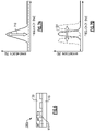
In certain embodiments, the EMI shield itself can be leveraged to control the electrical conductivity (or other properties) of the metal-to-insulator transition material 130. This concept is demonstrated with reference to FIGS. 3A, 3B, and 4. FIGS. 3A and 3B schematically illustrate an example of an aperture 100 b including an embedded EMI shield 310 and the metal-to-insulator transition material 130 disposed over the base layer 110 and the plurality of conductive wires 120 making up the EMI shield 310, as discussed above. In this example, the aperture 100 b also includes a cladding layer 140. FIG. 3B is a plan view, showing the EMI shield 310. In this example, the EMI shield 310 includes a rectangular grid of the conductive wires 120; however, those skilled in the art will appreciate that the EMI shield 310 may have other configurations. FIG. 3A is a cross-sectional view taken between the wires in one dimension of the EMI shield 310, such that only the conductive wires 120 running in the opposite dimension are shown. In certain examples, the metal-to-insulator transition material 130 can be integrated into an adhesive which bonds the base layer 110 and the cladding layer 140 together. Thus, the metal-to-insulator transition material 130 may be easily integrated into existing aperture architectures with minimal impact on SWaP-C.
According to certain examples, a control voltage, V, can be applied to all or to one or more selected conductive wires 120 of the EMI shield 310 to resistively heat the wires, which in turn may heat the metal-to-insulator transition material 130 in the region of the heated wires. Heating the metal-to-insulator transition material 130 may alter its electrical conductivity, thereby changing its transmission properties and the transmission properties of the aperture 100 b. This change can be controlled to apply over the whole aperture 100 b or one or more selected regions of the aperture 100 b by applying the controlled voltages to one or more selected conductive wires 120. By changing the applied control voltages, and the selected wires 120 to which the control voltages are applied, the transmission properties of the aperture 100 b can be dynamically and spatially controlled in real time.
FIG. 4 is a graph showing various characteristics of the aperture 100 b and the metal-to-insulator transition material 130 over time to illustrate operation of the dynamic aperture 100 b. In FIG. 4, trace 410 represents the electrical conductivity of the metal-to-insulator transition material 130, trace 420 represents the current flowing through the conductive wires 120 of the EMI shield 310, trace 430 represents the temperature of the metal-to-insulator transition material 130, and trace 440 represents the RF transmission of the aperture 100 b. As discussed above, one or more control voltages can be applied to some or all of the conductive wires 120 of the EMI shield 310, causing a current to flow through the wires 120 and heat them. The current flow and associated heating of the wires 120 causes the surrounding metal-to-insulator transition material 130 to heat, as shown by traces 420 and 430 in FIG. 4. The control voltage may be applied as a pulse, which in the illustrated example is a 1 millisecond (ms) pulse 450. The voltage applied and the duration of the pulse 450 may be selected to achieve a particular temperature rise in the metal-to-insulator transition material 130. In the example shown in FIG. 4, the temperature of the metal-to-insulator transition material 130 is raised to above a crystal melting temperature of the material (T>Tmelt) so as to change its material properties. At the end of the applied control voltage pulse 450, the current in the wires 120 is reduced, and the heated region of the metal-to-insulator transition material 130 cools, as shown by the drops in traces 420 and 430. Correspondingly, the electrical conductivity of the metal-to-insulator transition material 130 decreases, as shown by trace 410, and the RF transmission of the aperture 100 b (trace 440) increases; i.e., the aperture 100 b becomes more transmissive at the given frequency. The increase in RF transmission of the aperture 100 b is indicated by dimension 442, and in certain examples, may be as much as 12-15 dB.
As shown in FIG. 4, the RF transmission of the aperture 100 b can be returned to the original, or “steady state,” condition by applying another control voltage pulse to the EMI shield 310. In the illustrated example, this second pulse 460 is longer (30 ms in the example shown) and of lower intensity, that is, the current flow caused by the second control voltage pulse 460 is significantly lower than that caused by the first control voltage pulse 450, as may be seen with reference to trace 420. Accordingly, due to the lower current, the temperature of the metal-to-insulator transition material 130 increases, but not as much and may be maintained below the melting temperature (Tmelt>T>Tcrys). With the rise in temperature, the electrical conductivity of the metal-to-insulator transition material 130 increases (shown by trace 410) and the RF transmission of the aperture 100 b decreases until reaching the original, steady-state value, as shown by trace 440. At this point, the second control voltage pulse 460 may end. In certain example, the change in electrical conductivity of the metal-to-insulator transition material 130 may be as much as 10,000 times. The process illustrated in FIG. 4 may be repeated, optionally with variations in the levels of the control voltages applied, the duration of either or both control pulses 450, 460, and/or the selected conductive wires 120 to which the control voltages are applied, to dynamically control the RF transmission of the aperture 100 b.
As discussed above, individual ones or groups of the conductive wires 120 of the EMI shield 310 can be selectively biased with control voltages to control the temperature of the metal-to-insulator transition material 130 and the transmission properties of the apertures 100 a, 100 b. Accordingly, referring to FIG. 5, a system 500, such as an optical imaging system or RF system, (e.g., radar or RF communications) may include a aperture 100 and a controller 510 coupled to the aperture 100. The controller 510 may apply individually controllable bias voltages to the EMI shield 310 via one or more control lines 520. The controller 510 may include various electronic components, as would be understood by those skilled in the art, to perform the functionality of applying control voltage (and/or current) to the EMI shield 310, as discussed above, to achieve spatially localized and dynamic control of the transmission properties of the aperture 100. The controller 510 may be a dedicated controller associated with the aperture 100 or may be part of electronics included in the underlying optical or RF system with which the aperture 100 is used.
In the examples discussed above, the apertures 100 a, 100 b include an embedded EMI shield 310 that can be leveraged to adjust the properties of the metal-to-insulator material 130. However, as discussed above, in other examples, apertures may include other embedded structures, such as a frequency selective surface, for example. Accordingly, in other examples, these other structures can be used in combination with the metal-to-insulator transition material 130 to adjust the transmission properties of the aperture, and optionally can also be leveraged to control the conductivity of the metal-to-insulator transition material 130. For example, referring to FIG. 6 there is illustrated an example of an aperture 100 c that includes a frequency selective surface 610 along with the metal-to-insulator transition material 130 positioned over the base layer 110. In the example shown in FIG. 6, the frequency selective surface 610 include a plurality of discontinuous regions, which may be conductive. The plurality of discontinuous regions of the frequency selective surface 610 may have a variety of different shapes, including, for example, squares, rectangles, circles, rings, crosses (e.g. + shape), Y shapes, star shapes, or other geometric or non-geometric shapes. As discussed above, the frequency selective surface 610 may be configured to provide filtering of certain frequencies, for example, to produce a notch or bandpass filter within the aperture 100 c. According to certain embodiments, the metal-to-insulator transition material 130 can be controlled (e.g., via voltage, current, or temperature, as discussed above) to operate in combination with the frequency selective surface 610 to vary the filtering (transmission) properties of the aperture 100 c.
FIGS. 7A and 7B are graphs showing examples of a transmission profile of the aperture 100 c, including a bandpass filter at least partially produced by the frequency selective surface 610. In certain examples, the metal-to-insulator transition material 130 can be used to vary the degree of transmission in the passband of the filter, as indicated by arrow 710 in FIG. 7A. In further examples, the metal-to-insulator transition material 130 can be used to alter the range of frequencies corresponding to the passband of the filter, as indicated by arrow 720 in FIG. 7B. Thus, the amount of transmission and/or the frequency range of transmission of the aperture 100 c can be dynamically controlled using the combination of the frequency selective surface 610 and the metal-to-insulator transition material 130.
Thus, aspects and embodiments provide methods and apparatus to dynamically alter RF or optical transmission properties of an aperture that include integration of materials which exhibit an electrical metal-to-insulator transition due to changes in temperature into an aperture, integration of a heater structure into the material or aperture, driving the heater to heat the metal-to-insulator material to induce a change in the electrical conductivity of the metal-to-insulator material, and using that change in electrical conductivity of the metal-to-insulator transition material to alter the transmission properties of the aperture. As discussed above, the metal-to-insulator transition material may be integrated into existing aperture architectures with minimal impact on SWaP-C, and may be operated in combination with other existing structures in the aperture, such as EMI shields and frequency selective surfaces or other filtering structures. The approach disclosed herein provides a dynamic aperture that may exhibit improved noise performance relative to conventional static apertures.
Having described above several aspects of at least one embodiment, it is to be appreciated various alterations, modifications, and improvements will readily occur to those skilled in the art. Such alterations, modifications, and improvements are intended to be part of this disclosure and are intended to be within the scope of the invention. Accordingly, the foregoing description and drawings are by way of example only, and the scope of the invention should be determined from proper construction of the appended claims, and their equivalents.

Claims (11)

What is claimed is:
1. A dynamic aperture comprising:
a base layer;
a conductive structure disposed on the base layer; and
a layer of a metal-to-insulator transition material having a dynamically controllable electrical conductivity, the layer of the material being disposed over the base layer and the conductive structure, a transmission profile of the dynamic aperture being determined by a combination of the conductive structure and the layer of the material, and the transmission profile being dynamically alterable by controlling the electrical conductivity of the layer of the material.
2. The dynamic aperture of claim 1 wherein the conductive structure is an electromagnetic interference shield.
3. The dynamic aperture of claim 2 wherein the electromagnetic interference shield includes a plurality of conductive wires arranged in a two-dimensional grid.
4. The dynamic aperture of claim 3 further comprising a controller configured to apply a control voltage to at least a subset of the plurality of conductive wires to resistively heat the subset of the plurality of conductive wires and thereby heat a surrounding portion of the metal-to-insulator transition material to alter the electrical conductivity of the surrounding portion of the metal-to-insulator transition material.
5. The dynamic aperture of claim 1 wherein the conductive structure is a frequency selective surface.
6. The dynamic aperture of claim 5 wherein the frequency selective surface is configured to produce a bandpass filter in the transmission profile of the dynamic aperture, and wherein at least one of a range of frequencies included in a passband of the bandpass filter and a level of transmission in the passband of the bandpass filter is adjustable by controlling the electrical conductivity of the metal-to-insulator transition material.
7. The dynamic aperture of claim 1 further comprising a cladding layer disposed over the layer of the material.
8. The dynamic aperture of claim 7 wherein the layer of the material is integrated with an adhesive that bonds the cladding layer and the base layer together.
9. A dynamic aperture comprising:
a base layer;
a conductive structure disposed on the base layer; and
a layer of a material having a dynamically controllable electrical conductivity, the layer of the material being disposed over the base layer and the conductive structure, a transmission profile of the dynamic aperture being determined by a combination of the conductive structure and the layer of the material, and the transmission profile being dynamically alterable by controlling the electrical conductivity of the layer of the material, wherein the conductive structure is an electromagnetic interference shield that includes a plurality of conductive wires arranged in a two-dimensional and overlapping grid.
10. The dynamic aperture of claim 9 wherein the material having the dynamically controllable electrical conductivity is a metal-to-insulator transition material.
11. The dynamic aperture of claim 9 wherein the conductive structure is a frequency selective surface.
US16/537,212 2019-08-09 2019-08-09 Apertures with dynamically variable electromagnetic properties Active 2040-12-24 US11451309B2 (en)

Priority Applications (2)

Application Number Priority Date Filing Date Title
US16/537,212 US11451309B2 (en) 2019-08-09 2019-08-09 Apertures with dynamically variable electromagnetic properties
PCT/US2020/036736 WO2021029942A1 (en) 2019-08-09 2020-06-09 Apertures with dynamically variable electromagnetic properties

Applications Claiming Priority (1)

Application Number Priority Date Filing Date Title
US16/537,212 US11451309B2 (en) 2019-08-09 2019-08-09 Apertures with dynamically variable electromagnetic properties

Publications (2)

Publication Number Publication Date
US20210044364A1 US20210044364A1 (en) 2021-02-11
US11451309B2 true US11451309B2 (en) 2022-09-20

Family

ID=71944209

Family Applications (1)

Application Number Title Priority Date Filing Date
US16/537,212 Active 2040-12-24 US11451309B2 (en) 2019-08-09 2019-08-09 Apertures with dynamically variable electromagnetic properties

Country Status (2)

Country Link
US (1) US11451309B2 (en)
WO (1) WO2021029942A1 (en)

Citations (25)

* Cited by examiner, † Cited by third party
Publication number Priority date Publication date Assignee Title
US2644065A (en) 1948-12-31 1953-06-30 Bendix Aviat Corp Windshield temperature controller
DE2551366A1 (en) 1975-11-15 1977-05-26 Licentia Gmbh Radome for arctic conditions - has heating elements embedded in laminated material with inductive compensation for its capacitance
JPS6242209A (en) 1985-08-19 1987-02-24 Nec Corp Optical device
US5139850A (en) 1987-02-03 1992-08-18 Pilkington Plc Electromagnetic shielding panel
US5208603A (en) 1990-06-15 1993-05-04 The Boeing Company Frequency selective surface (FSS)
US5619365A (en) 1992-06-08 1997-04-08 Texas Instruments Incorporated Elecronically tunable optical periodic surface filters with an alterable resonant frequency
US6545500B1 (en) 1999-12-08 2003-04-08 John E. Field Use of localized temperature change in determining the location and character of defects in flat-panel displays
US6646605B2 (en) 2000-10-12 2003-11-11 E-Tenna Corporation Tunable reduced weight artificial dielectric antennas
US20050012677A1 (en) 2003-07-16 2005-01-20 Brown Stephen B. Dynamically variable frequency selective surface
US20050179614A1 (en) 2004-02-18 2005-08-18 Nagy Louis L. Dynamic frequency selective surfaces
US7173565B2 (en) * 2004-07-30 2007-02-06 Hrl Laboratories, Llc Tunable frequency selective surface
US20090096545A1 (en) 2007-10-12 2009-04-16 Los Alamos National Security Llc Dynamic frequency tuning of electric and magnetic metamaterial response
US7592957B2 (en) 2006-08-25 2009-09-22 Rayspan Corporation Antennas based on metamaterial structures
US7611746B2 (en) 2003-11-14 2009-11-03 Bridgestone Corporation Electromagnetic-wave-shielding light-transmitting window member and method for producing the same
US20100168935A1 (en) 2008-12-30 2010-07-01 Ppg Industries Ohio, Inc. Method of and system for maintaining operating performance of a transparency
US20140266517A1 (en) 2013-03-13 2014-09-18 The Penn State Research Foundation Radio frequency switch and processes of selectively regulating radio frequency energy transmission
US8889218B2 (en) 2009-03-12 2014-11-18 Ppg Industries Ohio, Inc. Foam window mount having an electric conductive layer over a light blocking layer
EP2916387A1 (en) 2014-03-04 2015-09-09 The Boeing Company Lightning protected radome system
US9146437B2 (en) 2013-01-31 2015-09-29 Gentex Corporation Electro-optic window assembly
US20170082572A1 (en) 2015-07-28 2017-03-23 Ppg Industries Ohio, Inc. Aerospace transparency having moisture sensors
US20170102601A1 (en) 2015-10-08 2017-04-13 Gentex Corporation Window assembly with infrared reflector
US20170273142A1 (en) 2014-08-22 2017-09-21 Bombardier Inc. Apparatus and method for controlled heating of a vehicle window
CN107402383A (en) 2017-09-11 2017-11-28 重庆邮电大学 A kind of bi-phase modulated plate and method for implementing radar frequency spectrum shift
CN108390134A (en) 2018-04-04 2018-08-10 南京航空航天大学 A kind of light-operated active frequencies selection surface and its feedback light, control and test method
US20190265570A1 (en) 2018-02-23 2019-08-29 The Boeing Company Electronic Window Array

Patent Citations (25)

* Cited by examiner, † Cited by third party
Publication number Priority date Publication date Assignee Title
US2644065A (en) 1948-12-31 1953-06-30 Bendix Aviat Corp Windshield temperature controller
DE2551366A1 (en) 1975-11-15 1977-05-26 Licentia Gmbh Radome for arctic conditions - has heating elements embedded in laminated material with inductive compensation for its capacitance
JPS6242209A (en) 1985-08-19 1987-02-24 Nec Corp Optical device
US5139850A (en) 1987-02-03 1992-08-18 Pilkington Plc Electromagnetic shielding panel
US5208603A (en) 1990-06-15 1993-05-04 The Boeing Company Frequency selective surface (FSS)
US5619365A (en) 1992-06-08 1997-04-08 Texas Instruments Incorporated Elecronically tunable optical periodic surface filters with an alterable resonant frequency
US6545500B1 (en) 1999-12-08 2003-04-08 John E. Field Use of localized temperature change in determining the location and character of defects in flat-panel displays
US6646605B2 (en) 2000-10-12 2003-11-11 E-Tenna Corporation Tunable reduced weight artificial dielectric antennas
US20050012677A1 (en) 2003-07-16 2005-01-20 Brown Stephen B. Dynamically variable frequency selective surface
US7611746B2 (en) 2003-11-14 2009-11-03 Bridgestone Corporation Electromagnetic-wave-shielding light-transmitting window member and method for producing the same
US20050179614A1 (en) 2004-02-18 2005-08-18 Nagy Louis L. Dynamic frequency selective surfaces
US7173565B2 (en) * 2004-07-30 2007-02-06 Hrl Laboratories, Llc Tunable frequency selective surface
US7592957B2 (en) 2006-08-25 2009-09-22 Rayspan Corporation Antennas based on metamaterial structures
US20090096545A1 (en) 2007-10-12 2009-04-16 Los Alamos National Security Llc Dynamic frequency tuning of electric and magnetic metamaterial response
US20100168935A1 (en) 2008-12-30 2010-07-01 Ppg Industries Ohio, Inc. Method of and system for maintaining operating performance of a transparency
US8889218B2 (en) 2009-03-12 2014-11-18 Ppg Industries Ohio, Inc. Foam window mount having an electric conductive layer over a light blocking layer
US9146437B2 (en) 2013-01-31 2015-09-29 Gentex Corporation Electro-optic window assembly
US20140266517A1 (en) 2013-03-13 2014-09-18 The Penn State Research Foundation Radio frequency switch and processes of selectively regulating radio frequency energy transmission
EP2916387A1 (en) 2014-03-04 2015-09-09 The Boeing Company Lightning protected radome system
US20170273142A1 (en) 2014-08-22 2017-09-21 Bombardier Inc. Apparatus and method for controlled heating of a vehicle window
US20170082572A1 (en) 2015-07-28 2017-03-23 Ppg Industries Ohio, Inc. Aerospace transparency having moisture sensors
US20170102601A1 (en) 2015-10-08 2017-04-13 Gentex Corporation Window assembly with infrared reflector
CN107402383A (en) 2017-09-11 2017-11-28 重庆邮电大学 A kind of bi-phase modulated plate and method for implementing radar frequency spectrum shift
US20190265570A1 (en) 2018-02-23 2019-08-29 The Boeing Company Electronic Window Array
CN108390134A (en) 2018-04-04 2018-08-10 南京航空航天大学 A kind of light-operated active frequencies selection surface and its feedback light, control and test method

Non-Patent Citations (5)

* Cited by examiner, † Cited by third party
Title
D. J. Park et al: "Electrically controllable THz asymmetric split-loop resonator with an outer square loop based on VO2," Optics Express, (2018) vol. 26, No. 13.
Hearn, David R. "Vacuum window optical power induced by temperature gradients", Earth Observing Systems IV (1999), pp. 1-12.
Jun-Hwan Shin et al: "Electrically controllable terahertz square-loop metamaterial based on VO2 thin film," Nanotechnology, Institute of Physics Publishing, (2016) vol. 27, No. 19.
Pilette et al. "Thermal Stresses in Double-Glazed Windows", Canadian Journal of Civil Engineering (1988) vol. 15, No. 5, pp. 807-814.
Shuai Zhao et al: "Electrically triggered dual-band tunable terahertz metamaterial band-pass filter based on Si3N4—VO2—Si3N4 sandwich," Chinese Physics B, (2019) vol. 28, No. 5.

Also Published As

Publication number Publication date
US20210044364A1 (en) 2021-02-11
WO2021029942A1 (en) 2021-02-18

Similar Documents

Publication Publication Date Title
US11362699B2 (en) Mobile terminal
KR102342031B1 (en) Internal heater for RF aperture
US20150229030A1 (en) Heatable window with high-pass frequency selective surface
CN105244627B (en) Tunable single is to microwave stealth device
CN109765734A (en) A kind of liquid crystal display panel and display device
CN111512130B (en) Optically transparent electromagnetic shielding assembly
US20240008234A1 (en) Optical window with integrated temperature sensing
US11451309B2 (en) Apertures with dynamically variable electromagnetic properties
Belyaev et al. Nonlinear behavior of plasma antenna vibrator
US11264691B2 (en) Ground plane heater
US20210408651A1 (en) Tunable band-stop filter, method of driving the same and electronic device
US20210013605A1 (en) Antenna phase shifter with integrated dc-block
EP3595087B1 (en) Meta-structure having complex properties and apparatus using same
Inami et al. Experimental observation of multi-functional plasma-metamaterial composite for manipulation of electromagnetic-wave propagation
US11233333B2 (en) Tunable waveguide system
Tricas et al. Dynamic control of the shielding effectiveness of optically transparent Screens
Ding et al. Adaptive high-level isolation between two closely placed copolarized antennas using tunable screen
US10730483B2 (en) Transparent window plate provided with defogging heat wires
KR20200129757A (en) Antenna Device Using Metal Frame For Improving Signal Interference and Electronic Device Including That Antenna Device
US10575449B1 (en) Combined high frequency EMI shield and substrate heater using a thin film
US11715871B2 (en) Iris heater structure for uniform heating
KR20240032098A (en) Intelligent Noise Mitigation for Electronic Devices
KR20230051946A (en) Detector based on transistor-antenna
DE102017103074A1 (en) IMPEDANT SURFACE TREATMENT FOR WELDING SURFACE WAVES AND IMPROVING ANTENNA WINNING ON GLASS
CN117767014A (en) Radome, antenna assembly and electronic equipment

Legal Events

Date Code Title Description
FEPP Fee payment procedure

Free format text: ENTITY STATUS SET TO UNDISCOUNTED (ORIGINAL EVENT CODE: BIG.); ENTITY STATUS OF PATENT OWNER: LARGE ENTITY

AS Assignment

Owner name: RAYTHEON COMPANY, MASSACHUSETTS

Free format text: ASSIGNMENT OF ASSIGNORS INTEREST;ASSIGNORS:GROSSE, KYLE;FRAZIER, GARY A.;TRENT, CATHERINE;AND OTHERS;SIGNING DATES FROM 20190908 TO 20191002;REEL/FRAME:051221/0543

STPP Information on status: patent application and granting procedure in general

Free format text: DOCKETED NEW CASE - READY FOR EXAMINATION

STPP Information on status: patent application and granting procedure in general

Free format text: NON FINAL ACTION MAILED

STPP Information on status: patent application and granting procedure in general

Free format text: RESPONSE TO NON-FINAL OFFICE ACTION ENTERED AND FORWARDED TO EXAMINER

STPP Information on status: patent application and granting procedure in general

Free format text: NOTICE OF ALLOWANCE MAILED -- APPLICATION RECEIVED IN OFFICE OF PUBLICATIONS

STCF Information on status: patent grant

Free format text: PATENTED CASE