US11443930B2 - Solid-state charge detector - Google Patents
Solid-state charge detector Download PDFInfo
- Publication number
- US11443930B2 US11443930B2 US16/889,700 US202016889700A US11443930B2 US 11443930 B2 US11443930 B2 US 11443930B2 US 202016889700 A US202016889700 A US 202016889700A US 11443930 B2 US11443930 B2 US 11443930B2
- Authority
- US
- United States
- Prior art keywords
- charge
- charge amplifier
- detector
- amplifier
- differential
- Prior art date
- Legal status (The legal status is an assumption and is not a legal conclusion. Google has not performed a legal analysis and makes no representation as to the accuracy of the status listed.)
- Active, expires
Links
Images


Classifications
-
- H—ELECTRICITY
- H01—ELECTRIC ELEMENTS
- H01J—ELECTRIC DISCHARGE TUBES OR DISCHARGE LAMPS
- H01J49/00—Particle spectrometers or separator tubes
- H01J49/02—Details
- H01J49/022—Circuit arrangements, e.g. for generating deviation currents or voltages ; Components associated with high voltage supply
-
- G—PHYSICS
- G01—MEASURING; TESTING
- G01R—MEASURING ELECTRIC VARIABLES; MEASURING MAGNETIC VARIABLES
- G01R29/00—Arrangements for measuring or indicating electric quantities not covered by groups G01R19/00 - G01R27/00
- G01R29/24—Arrangements for measuring quantities of charge
-
- H—ELECTRICITY
- H01—ELECTRIC ELEMENTS
- H01J—ELECTRIC DISCHARGE TUBES OR DISCHARGE LAMPS
- H01J49/00—Particle spectrometers or separator tubes
- H01J49/02—Details
- H01J49/025—Detectors specially adapted to particle spectrometers
-
- H—ELECTRICITY
- H03—ELECTRONIC CIRCUITRY
- H03F—AMPLIFIERS
- H03F3/00—Amplifiers with only discharge tubes or only semiconductor devices as amplifying elements
- H03F3/04—Amplifiers with only discharge tubes or only semiconductor devices as amplifying elements with semiconductor devices only
- H03F3/08—Amplifiers with only discharge tubes or only semiconductor devices as amplifying elements with semiconductor devices only controlled by light
- H03F3/087—Amplifiers with only discharge tubes or only semiconductor devices as amplifying elements with semiconductor devices only controlled by light with IC amplifier blocks
-
- H—ELECTRICITY
- H03—ELECTRONIC CIRCUITRY
- H03F—AMPLIFIERS
- H03F3/00—Amplifiers with only discharge tubes or only semiconductor devices as amplifying elements
- H03F3/45—Differential amplifiers
- H03F3/45071—Differential amplifiers with semiconductor devices only
- H03F3/45076—Differential amplifiers with semiconductor devices only characterised by the way of implementation of the active amplifying circuit in the differential amplifier
- H03F3/45179—Differential amplifiers with semiconductor devices only characterised by the way of implementation of the active amplifying circuit in the differential amplifier using MOSFET transistors as the active amplifying circuit
- H03F3/45183—Long tailed pairs
- H03F3/45192—Folded cascode stages
-
- H—ELECTRICITY
- H03—ELECTRONIC CIRCUITRY
- H03F—AMPLIFIERS
- H03F3/00—Amplifiers with only discharge tubes or only semiconductor devices as amplifying elements
- H03F3/45—Differential amplifiers
- H03F3/45071—Differential amplifiers with semiconductor devices only
- H03F3/45076—Differential amplifiers with semiconductor devices only characterised by the way of implementation of the active amplifying circuit in the differential amplifier
- H03F3/45179—Differential amplifiers with semiconductor devices only characterised by the way of implementation of the active amplifying circuit in the differential amplifier using MOSFET transistors as the active amplifying circuit
- H03F3/45273—Mirror types
-
- H—ELECTRICITY
- H03—ELECTRONIC CIRCUITRY
- H03F—AMPLIFIERS
- H03F3/00—Amplifiers with only discharge tubes or only semiconductor devices as amplifying elements
- H03F3/45—Differential amplifiers
- H03F3/45071—Differential amplifiers with semiconductor devices only
- H03F3/45076—Differential amplifiers with semiconductor devices only characterised by the way of implementation of the active amplifying circuit in the differential amplifier
- H03F3/45475—Differential amplifiers with semiconductor devices only characterised by the way of implementation of the active amplifying circuit in the differential amplifier using IC blocks as the active amplifying circuit
-
- H—ELECTRICITY
- H03—ELECTRONIC CIRCUITRY
- H03F—AMPLIFIERS
- H03F3/00—Amplifiers with only discharge tubes or only semiconductor devices as amplifying elements
- H03F3/45—Differential amplifiers
- H03F3/45071—Differential amplifiers with semiconductor devices only
- H03F3/45479—Differential amplifiers with semiconductor devices only characterised by the way of common mode signal rejection
- H03F3/45632—Differential amplifiers with semiconductor devices only characterised by the way of common mode signal rejection in differential amplifiers with FET transistors as the active amplifying circuit
- H03F3/45636—Differential amplifiers with semiconductor devices only characterised by the way of common mode signal rejection in differential amplifiers with FET transistors as the active amplifying circuit by using feedback means
- H03F3/45641—Measuring at the loading circuit of the differential amplifier
- H03F3/45659—Controlling the loading circuit of the differential amplifier
-
- H—ELECTRICITY
- H03—ELECTRONIC CIRCUITRY
- H03F—AMPLIFIERS
- H03F3/00—Amplifiers with only discharge tubes or only semiconductor devices as amplifying elements
- H03F3/70—Charge amplifiers
-
- H—ELECTRICITY
- H03—ELECTRONIC CIRCUITRY
- H03G—CONTROL OF AMPLIFICATION
- H03G1/00—Details of arrangements for controlling amplification
- H03G1/0005—Circuits characterised by the type of controlling devices operated by a controlling current or voltage signal
- H03G1/0088—Circuits characterised by the type of controlling devices operated by a controlling current or voltage signal using discontinuously variable devices, e.g. switch-operated
- H03G1/0094—Circuits characterised by the type of controlling devices operated by a controlling current or voltage signal using discontinuously variable devices, e.g. switch-operated using switched capacitors
-
- H—ELECTRICITY
- H03—ELECTRONIC CIRCUITRY
- H03G—CONTROL OF AMPLIFICATION
- H03G3/00—Gain control in amplifiers or frequency changers without distortion of the input signal
- H03G3/20—Automatic control
- H03G3/30—Automatic control in amplifiers having semiconductor devices
-
- H—ELECTRICITY
- H03—ELECTRONIC CIRCUITRY
- H03G—CONTROL OF AMPLIFICATION
- H03G3/00—Gain control in amplifiers or frequency changers without distortion of the input signal
- H03G3/20—Automatic control
- H03G3/30—Automatic control in amplifiers having semiconductor devices
- H03G3/3084—Automatic control in amplifiers having semiconductor devices in receivers or transmitters for electromagnetic waves other than radiowaves, e.g. lightwaves
-
- H—ELECTRICITY
- H03—ELECTRONIC CIRCUITRY
- H03F—AMPLIFIERS
- H03F2203/00—Indexing scheme relating to amplifiers with only discharge tubes or only semiconductor devices as amplifying elements covered by H03F3/00
- H03F2203/45—Indexing scheme relating to differential amplifiers
- H03F2203/45428—Indexing scheme relating to differential amplifiers the CMCL comprising a comparator circuit using a four inputs dif amp
-
- H—ELECTRICITY
- H03—ELECTRONIC CIRCUITRY
- H03F—AMPLIFIERS
- H03F2203/00—Indexing scheme relating to amplifiers with only discharge tubes or only semiconductor devices as amplifying elements covered by H03F3/00
- H03F2203/45—Indexing scheme relating to differential amplifiers
- H03F2203/45514—Indexing scheme relating to differential amplifiers the FBC comprising one or more switched capacitors, and being coupled between the LC and the IC
-
- H—ELECTRICITY
- H03—ELECTRONIC CIRCUITRY
- H03F—AMPLIFIERS
- H03F2203/00—Indexing scheme relating to amplifiers with only discharge tubes or only semiconductor devices as amplifying elements covered by H03F3/00
- H03F2203/45—Indexing scheme relating to differential amplifiers
- H03F2203/45526—Indexing scheme relating to differential amplifiers the FBC comprising a resistor-capacitor combination and being coupled between the LC and the IC
Definitions
- This invention relates generally to charge detection. More specifically, the invention is a charge detector that utilizes a high-gain, differential solid-state amplifier with active reset and a novel technique to measure the gain of a charge amplifier using a custom optoelectronic system.
- Charge detection is important to a large variety of scientific and commercial applications, including mass spectrometry, DNA processing, and scientific imaging.
- One common method is electron multiplication.
- An electron multiplier (EM) relies on secondary electron emission by collision of electrons with one or more surfaces.
- electron multipliers require a high supply voltage (typically around 1000 V) and a vacuum or near vacuum environment for operation.
- IDELs consist of an amplifier circuit connected to a charge-collection electrode.
- the charge of an incident particle can either be transferred indirectly through an image charge or directly through impact on a conductive surface.
- Direct impact electrodes are often referred to as Faraday cups and are commonly used in applications such as mass spectrometry where mass-analyzed ions impact a detection electrode.
- Indirect charge induction methods are used in charge detection mass spectrometry (CDMS) as well as Fourier transform ion cyclotron resonance mass spectrometry and orbitraps.
- the present invention is a system and method for providing a charge detector that utilizes small feedback capacitors in a low-noise, high-gain, system that combines a differential topology in a solid-state amplifier implemented in a complementary metal-oxide semiconductor (CMOS) process with active reset, thereby achieving high dynamic range and robust operations.
- CMOS complementary metal-oxide semiconductor
- a custom optoelectronic system is used to measure gain, and while operating at a sampling frequency of 10 kHz, the active reset extends the dynamic range of the charge detector.
- the charge amplifier is the first instance of a charge detector that combines a differential topology, active reset, and small feedback capacitors.
- the optoelectronic system injects an adjustable input photocurrent to precisely quantify the charge detector's gain without the need for a known calibration capacitance.
- the charge amplifier is directly wire-bonded to a printed circuit board (PCB) that has a built-in charge collector such as a Faraday cup.
- PCB printed circuit board
- FIG. 1 is an amplifier circuit of the prior art.
- FIG. 2 is a modified amplifier circuit of the prior art showing an improved feedback design.
- FIG. 3 is a block diagram of the embodiments of the invention.
- FIG. 4 is a detailed circuit diagram of the components in the charge detector, including a charge amplifier, identical and programmable feedback capacitors and feedback resistors, electrostatic discharge circuitry, a common mode feedback circuit, and an output buffer.
- FIG. 5A is an expanded circuit diagram of the internal layout of the charge amplifier.
- FIG. 5B is a view of a noise sweep for different values of transistor width, length, and tail current.
- FIG. 5C is a close-up view of the noise sweep in FIG. 5B .
- FIG. 5D is an expanded circuit diagram of the internal layout of the common mode feedback circuit.
- FIG. 6 is a table showing an example of values that were used for the charge detector 30 shown in FIGS. 4, 5A and 5D .
- FIG. 7 is a charge detector output waveform for a constant, continuous input charge.
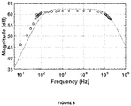
- FIG. 8 is Simulated (line) and measured (points) voltage frequency response of the charge detector.
- FIG. 9 is charge detector gain measurement setup using a custom optoelectronic system, wherein the dotted box represents additional circuitry for photodiode current measurements.
- FIG. 10 is charge-voltage gain versus detector input capacitance. Simulation results are shown as a solid line and measurements as points.
- FIG. 11 is Input-referred noise versus detector input capacitance. Simulation results are shown as a solid line and measured values as points
- FIG. 12A is modulated photodiode current as measured by a transimpedance amplifier.
- FIG. 12B is detector response to a modulated input current over 400 acquisition cycles.
- the detector response has been processed by extracting ⁇ V's.
- FIG. 13A is raw output of the detector from a step input current over six acquisition cycles.
- FIG. 13B is a signal taken from a function generator that was used to modulate the laser driver.
- FIG. 14 is a block diagram of a free-space input charge test setup using electrospray.
- FIG. 15 is a charge detector response to an electrospray pulse at a selected sample rate and acquisition duty cycle.
- a second performance barrier for IDEL amplifier circuits is that they have typically utilized a single-ended configuration.
- Single-ended topologies are known to suffer from sensitivity to supply voltage noise, radio frequency (RF) interference, ground loops, self-coupling, etc., thus significantly reducing SNR.
- RF radio frequency
- a last performance barrier may be that contemporary devices may rely on a feedback resistor to passively reset the charge accumulated at the feedback capacitor.
- a passive reset is simply too slow and the amplifier output may quickly saturate, and thus compromising the data acquired.
- the embodiments of the invention described herein combine improvements and solutions to all three of these barriers to thereby achieve a charge detector design having substantial benefits over the prior art.
- the dramatically increased gain afforded by the small feedback capacitance, the improved noise performance of the differential topology, and the flexibility to operate in a variety of charge sensing situations enabled by the active reset make the embodiments of the invention high-performing in a wide range of mass spectrometry and space instrumentation applications.
- FIG. 1 shows that while a direct realization of this idea entails a single shunt capacitor C 10 with one end connected to ground and the other end acting as the charge target, the circuit (usually an amplifier 12 ) sensing a voltage V 14 across the capacitor C inevitably introduces a parasitic capacitance Cp 16 that is in parallel to C.
- the parasitic capacitance may come from the amplifier's input device, packaging, PCB trace, cabling, shielding, etc.
- Parasitic capacitance Cp 16 may also vary across different components, temperature, bias voltage, and be nonlinear, thereby creating uncertainties in the effective total capacitance. This makes it difficult to precisely calculate the incident charge for an output voltage.
- FIG. 2 shows that to solve this issue, a practical implementation of the charge detector typically assumes the alternative topology.
- an amplifier 18 maintains a virtual ground at node X 20 .
- an output voltage V 22 is much less sensitive to parasitic capacitance Cp 24 if the amplifier's open-loop gain is large. In the limit that the open-loop gain is infinity, Cp 24 has no effect on V 22 at all.
- the gain of the charge detector is ⁇ 1/C, it is desirable to minimize C 26 so as to increase the gain to thereby relax the noise requirements of the subsequent stages, and to improve the overall SNR.
- active reset of the accumulated charge may be necessary in applications where the input charge is large to avoid amplifier saturation.
- a differential implementation of the topology may reduce a charge detector circuit's sensitivity to noise and interference.
- the embodiments of the charge detector may be comprised of a Faraday cup that is coupled to a custom integrated charge amplifier fabricated using CMOS technology.
- FIG. 3 shows the elements of the embodiments of the invention in a block diagram.
- a central element of the charge detector 30 is a charge amplifier 32 .
- the charge amplifier 32 may have a set of programmable and non-programmable feedback capacitors and a feedback resistor on each of the differential inputs of the charge amplifier.
- Each set of the programmable and non-programmable feedback capacitors and the feedback resistor may be identical to the other.
- the embodiments may also include electrostatic discharge circuitry 36 on each of the differential inputs of the charge amplifier 32 .
- a common mode feedback (CMFB) circuit 38 is coupled to both outputs of the charge amplifier 32 and an output signal is sent to the charge amplifier to thereby dynamically control the gate voltage in the amplifier to force the output common mode to the reference voltage Vcm of the CMFB circuit.
- an output buffer 40 coupled to each of the outputs of the charge amplifier may increase the driving strength for large off-chip loads.
- FIGS. 4, 5A, and 5D provide a more detailed look at the charge detector circuitry 30 shown in the block diagram of FIG. 3 .
- this figure shows additional detail regarding the charge detector 30 elements 32 , 34 , 36 , 38 and 40 , and represents a differential charge amplifier with active reset and small feedback capacitors.
- feedback capacitors Cf 1 and Cf 2 set the charge-voltage gain of a closed-loop detector.
- Cf 1 may only be 10 fF, thus achieving at least an order of magnitude increase in the detector gain as compared to a discrete design that must rely on the smallest commercially available discrete capacitor (0.1 pF).
- the integrated feedback capacitors Cf 1 and Cf 2 also enjoy much tighter tolerances (about 5%) in comparison to discrete capacitors (50%), making it possible to have a vastly more consistent gain.
- the feedback capacitor Cf 2 (shown here as 90 fF) may be programmably activated to lower the detector gain to avoid amplifier saturation for large inputs.
- the feedback resistor Rf establishes the input bias voltage of the amplifier. This feedback resistor may be realized using pseudo-resistors to obtain a large value of about 128 a) to thereby create a small high-pass corner of about 55 Hz for the input.
- Electrostatic discharge (ESD) events during the handling and assembly process of the charge detector 30 can blow out transistors and render the detector useless.
- two large AC-coupling capacitors Cin may be incorporated at the inputs to decouple the amplifier's virtual grounds (Vx nodes) to allow for the placement of ESD diodes (D 1 and D 2 ) to protect the sensitive elements.
- the diodes are designed to sense high voltages caused by ESD events and divert the resulting currents to the rail or ground.
- the ESD diodes D 1 and D 2 have been selected to have equal leakages such that the equilibrium voltage established between them is the same as the reset voltage VRST for quick settling.
- FIG. 5A is an expanded circuit diagram of the charge amplifier 32 .
- the charge amplifier 32 may adopt a differential folded cascode topology for a large input common-mode range.
- the noise of the charge amplifier 32 is dominated by the differential transistor pair M 1 and M 2 . Therefore, the sizes of transistors M 1 and M 2 and their bias current have been carefully selected to achieve low noise.
- transistors M 9 and M 10 are degenerated by resistors R 1 and R 2 to thereby improve the noise performance. With the selected values for the transistors and resistors, the charge amplifier 32 exhibits an open-loop gain of 93 dB, open-loop bandwidth of 6.3 kHz, and an equivalent noise bandwidth of about 400 MHz.
- An important feature of the embodiments of the invention is minimizing the noise generated by the charge amplifier 32 . Therefore, the values of the differential transistor pair M 1 and M 2 may be an important factor in achieving the low noise of the charge detector 30 because the differential transistors limit the noise performance of the entire design, as well as contributing most of the noise.
- Input parasitic capacitance also affects the noise of the charge amplifier 32 .
- those skilled in the art may need to optimize the size of the differential transistor pair, as well as optimizing the tail current.
- Optimizing the size of the differential transistor pair may be accomplished by constructing a Cadence testbench.
- the Cadence testbench allows a Cadence simulator to sweep input transistors sizes W and L at different tail currents.
- the input parasitic capacitance is composed of the detector capacitance and gate capacitance from the differential input transistors.
- an off-chip detector capacitance for the differential input transistors.
- a 2 pF off-chip detector capacitance was selected. It should be understood that if the off-chip capacitance will be different than 2 pF, then the values of W and L of the differential input transistors will change. Thus, optimization of the size of the differential input transistors must be determined for the desired off-chip capacitance.
- FIG. 5B is a view of a simulation of input noise electron sweeps for different values of width (W) in micrometers, length (L) in micrometers and I (tail current).
- W width
- L length
- I tail current
- the testbench it first acquires output noise current through the IPRB at the Drain of the differential pair of input transistors M 1 and M 2 . Then, the result is divided by gm to obtain the input noise voltage. Finally, the equivalent noise electron was converted through 2 pF detector capacitance and transistor gate capacitance Cgg for different values of W, L and I.
- the different transistor values used for a noise sweep include W from (100-500 um), L from (0.18-1 um) and Id (tail current) from (10 uA-50 uA).
- FIG. 5C is a view of a display screen of an oscilloscope showing various noise sweeps results.
- FIG. 5D is an expanded view of the common mode feedback (CMFB) circuit 38 .
- the CMFB circuit 38 may sense the output voltages and dynamically adjust Vcmfb which controls the gate voltage of transistors M 11 and M 12 to force the output common mode to the reference voltage Vcm.
- the CMFB circuit 38 may function as an amplifier that has degenerated transistor input pairs (M 15 -M 18 ) for stability and degenerated current sources (M 19 -M 22 ) for low-noise.
- Vcm may be tuned from off-chip for easy debugging.
- the output buffer 40 increases the driving strength for large off-chip loads while the reset switches SRST in the ESD circuitry 36 actively clear the accumulated charge by shorting the inputs to VRST.
- An on-chip shift register may now generate a reset signal and programmable controls.
- the charge amplifier 32 may consume a total of 5.54 mW from a 1.8 V power supply.
- FIG. 6 is a table showing an example of values that were used for the charge detector 30 shown in FIGS. 4, 5A and 5D .
- the table includes values for the width and length of transistors and the values of some resistors in the charge detector 30 . It should be understood that these are values selected for a 2 pF off-chip detector capacitance, and that the values of the transistors and resistors may change for a different off-chip detector capacitance. Accordingly, the table is showing examples only, and should not be considered as limiting the claims.
- a custom 2-layer PCB measuring 2.5′′ ⁇ 3.75′′ has been designed to house the charge amplifier and the Faraday cup.
- a 1 cm ⁇ 1 cm Faraday cup may be provided as the top PCB metal layer, which reduces integration complexity and minimizes the distance between the Faraday cup and the charge amplifier. This reduced routing distance lowers the parasitic capacitance of the amplifier input, thereby improving noise performance.
- the amplifier may be directly wire-bonded to the PCB to avoid parasitic capacitance from a chip package. SMA connectors may be used for the supply voltage and charge detector test inputs/outputs to minimize noise coupling. Furthermore, a discrete regulator on the PCB generates a low-noise 1.8 V power supply for the amplifier.
- FIG. 7 illustrates the operational stages of the charge detector 30 .
- the charge detector output waveform shown is for a constant, continuous input charge.
- switches SRST shown in FIG. 4 short the amplifier inputs to VRST, thereby zeroing the amplifier differential output Vout.
- the SRST switches are turned off, allowing an input charge incident on the Faraday cup which is connected to input Vin+ to be accumulated on the feedback capacitors Cf 1 , or Cf 1 and Cf 2 .
- Input Vin ⁇ is coupled to an AC ground by a large capacitor so that the differential amplifier converts the single-ended input to a differential signal for robustness against supply noise, common-mode noise, RF interference, etc.
- the charge detector has the option to be re-configured to accept a differential input charge by utilizing both inputs.
- the output is a voltage ramp proportional to the integrated charge.
- the reset switches SRST are activated, thereby zeroing the voltage on Vout.
- the charge detector operates with a sample rate of up to 10 kHz with a user-determined acquisition duty cycle.
- the differential output may be digitized by an oscilloscope for analysis.
- the total charge collected during one acquisition period may be calculated by taking the change in voltage ( ⁇ V) of Vout during the acquisition period and dividing it by the charge-voltage gain. Therefore, the charge-voltage gain of the charge detector must be accurately characterized for this calculation.
- the frequency response of the amplifier in the embodiments of the invention was tested using a high-precision, low-voltage generator. The results of this test along with a comparison to simulated values is shown in FIG. 8 .
- the response exhibits a bandpass profile where the mid-band gain is set by Cin/Cf 1 , the high-pass corner by 1/(RfCf 1 ), and the lowpass corner by 1/(RoutCeff) where Rout is the output resistance of the amplifier and Ceff is the effective capacitive loading at the output of the amplifier.
- the amplifier demonstrates an excellent agreement between simulation (done using Cadence design and simulation tools) and measurements in both the gain (62 dB) and upper/lower corner frequencies (55 Hz/160 kHz).
- the accumulated charge on a collection electrode connected to an amplifier may be calculated by taking the voltage change at the amplifier's output and dividing it by the charge-voltage gain. Therefore, the charge-voltage gain of the detector must be accurately characterized.
- the embodiments of the invention include a new technique for determining the charge-voltage gain without having a known calibration capacitance.
- the technique employs a custom optoelectronic setup as shown in FIG. 9 .
- the purpose of the testing system shown in FIG. 9 is to generate an extremely low and adjustable current (e.g. in hundreds of pA), injecting it into the charge detector 30 , and then observing the charge detector output to calculate the gain.
- an extremely low and adjustable current e.g. in hundreds of pA
- the testing system shown in FIG. 9 uses a low power, single-mode Fabry Perot laser diode 50 (about 1 mW) with an output wavelength of 635 nm.
- the photodiode 52 that generates the test current is an Opto Diode model ODD-1W, a red-light enhanced silicon diode, operating under a reverse bias of 0.9 V.
- ODD-1W Opto Diode model
- Several different photodiodes of this model were used for testing and each of their parasitic capacitances was measured to be between 6.2 pF and 6.4 pF with leakage currents ranging from 27 pA to 33 pA.
- the parasitic capacitance was accounted for during data acquisition because it affects the gain of the charge amplifier 32 .
- a standard laser diode driver 54 supplied the laser diode with 50 mA of current.
- the light produced by the laser diode 50 was then guided through a fiber optic cable 64 and into an optical attenuator 56 .
- This attenuated light was then guided to the photodiode 52 through another fiber optic cable 66 .
- This fiber optic cable 66 was connected to the photodiode 52 by a black, 3D printed, double-sided socket.
- the socket attached the laser fiber cable 66 output to the top of the active area of the photodiode 52 , which served to provide a secure connection as well as to block out ambient light, thereby allowing consistent measurements.
- a picoammeter 58 measured the current through the reverse-biased photodiode 52 .
- the measurements were taken at various laser attenuation levels in order to characterize the amount of current flowing from the photodiode 52 .
- the current was measured at laser attenuation levels between 30 to 40 dB. At these levels, the measured current ranged from around 100 pA to 775 pA.
- the picoammeter 58 was replaced with the charge detector 30 .
- the gain of the charge amplifier 32 was calculated using equations 1-3 below, with tAQU being the time duration of the acquisition period, I the input current measured by the picoammeter 58 , q the elementary charge, and n the total number of elementary charges accumulated during acquisition.
- the minimum amount of charge used was limited by the dark current of the photodiode 52 , which was 33 pA. With a reset frequency of 10 kHz, and an approximately 50% acquisition duty cycle, the minimum number of charges equates to 9,476.
- the gain of the charge detector 30 was measured for a range of input capacitances which model the loading from the Faraday cup and other PCB components. This allows the user to predict the detector gain for a given input loading.
- the input capacitance was swept by connecting discrete capacitors in parallel with the photodiode 52 . The gain was then measured at each capacitance point using the optoelectronic setup described in FIG. 9 . The results are shown in FIG. 10 .
- the minimum input capacitance tested was 11 pF.
- the highest gain measured was 8.9 ⁇ V/e ⁇ at 11 pF and it decreases to 1.7 ⁇ V/e ⁇ at 94 pF.
- the maximum difference between measured and simulated (using Cadence design software) gains from this sweep was 11%. Such a small discrepancy may be explained by errors of the feedback capacitors in the charge detector 30 , as well as system noise and instrumentation errors.
- the noise of the charge detector 30 was measured by acquiring the charge detector output with a floating input node and dividing the output RMS value by the charge detector gain.
- the output RMS noise was measured using an oscilloscope 62 with a bandwidth of 2 GHz over a time window of just under 10 ms. Similar to the gain measurement, the input capacitance was varied to study its effect on the noise.
- FIG. 11 shows the result of this measurement.
- the charge detector 30 exhibits a noise of 475 e ⁇ with a 4.4 pF (simulated noise floor at this input capacitance is 381 e ⁇ ) load and it increases to 6352 e ⁇ at 87 pF.
- the measured noise shows larger deviation from the simulation for large input capacitances. This may be due to the increased sensitivity from the exponential profile of the noise curve as the input capacitance increases, or from external noise picked up from the test input capacitors. It is worth noting that should the input capacitance be reduced to 1 pF, the noise floor would fall to 334 e ⁇ .
- the input current from the system shown in FIG. 9 was varied by modulating the laser diode 50 .
- This test helped to determine the charge detector's ability to recreate a time-varying input, such as from a mass spectrometer.
- a function generator was used to apply a square wave signal of 250 mVpp at 50 Hz to the laser driver 54 .
- a transimpedance amplifier was connected to the photodiode to record the current.
- the laser signal was optically attenuated by 15 dB, producing a high current level of 73 nA and a low current level of 49 pA through the photodiode 52 .
- the TIA exhibited a current-to-voltage gain of roughly 550 kV/A.
- the voltage output of the TIA is shown in FIG. 12A , confirming the correct waveform.
- the TIA was then replaced by the charge detector 30 of the present invention.
- attenuation levels needed to be much higher than those used in the TIA tests.
- the following tests were performed at an optical attenuation level of 45 dB, thus the current input to the charge detector 30 was 30 dB less than that seen by the TIA.
- the resulting modulated input signal featured a current square wave with a 49 pA low level and 74 pA high level.
- the detector output waveform is shown in FIG. 13A .
- the figures show the raw output of the charge detector 30 from a step input current over six acquisition cycles.
- FIG. 13B shows the signal taken from the function modulator (signal generator) 60 that was used to modulate the laser driver 54 .
- the change in the amplitudes of the sawtooth waveforms coincided with the change in the input current (when the modulating voltage stepped up) as expected.
- the output was segmented by a sync signal that indicates the start and end times of the acquisition period.
- the ⁇ V in each of these acquisition periods was extracted by a processing program resulting in the waveform shown in FIG. 12B .
- the processed output shows a square-wave response from the square-wave input in agreement with the TIA waveform, validating the dynamic performance of the charge detector 30 .
- the voltage offset from zero of the square wave shown in FIG. 12B is the result of the dark current produced by the photodiode 52 , while in FIG. 12A no such offset is apparent due to the drastically higher levels of current used in those tests.
- an electrospray system 72 was utilized to produce charged methanol (MeOH) droplets 74 as depicted in FIG. 14 .
- the charged droplets 74 were projected to the Faraday cup 70 by a 3,000 V power supply 76 through a capillary tube 78 .
- the charge detector 30 was placed in an aluminum shielding box and the capillary tube 78 was inserted into the box via a small opening.
- the embodiments of the invention and the testing described above show that a charge detector 30 has been created with the maximum experimental gain of just under 9 ⁇ V/e ⁇ and an observed single-pass noise floor of 475 e ⁇ rms (with the potential to fall to 334 e ⁇ given a lower input capacitance).
- the embodiments may be defined as the following.
- the embodiments may be a method for operating a low power, differential, solid-state charge detector with active reset with the method comprised of the steps of providing a charge collector, providing a charge amplifier having differential inputs with transistors to thereby reduce sensitivity to noise and interference, wherein the charge collector is coupled to the charge amplifier, providing a first feedback capacitor in parallel with a feedback resistor on each of the differential inputs of the charge amplifier, and wherein the first feedback capacitor is less than 50 fFarads.
- An important feature may be optimizing the differential input transistors of the charge amplifier to thereby decrease the noise of the charge detector, providing an active reset switch on the differential inputs for performing an active reset of the charge amplifier, providing a common mode feedback circuit coupled to both outputs of the charge amplifier, resetting the charge amplifier using the active reset switch, and then measuring the charge on the charge collector over a period of time at the outputs of the charge amplifier.
Abstract
Description
Q in =t AQU ×I Equation 1:
n=Q in /q Equation 2:
GAIN=ΔV/n Equation 3:
Claims (42)
Priority Applications (1)
| Application Number | Priority Date | Filing Date | Title |
|---|---|---|---|
| US16/889,700 US11443930B2 (en) | 2019-08-15 | 2020-06-01 | Solid-state charge detector |
Applications Claiming Priority (4)
| Application Number | Priority Date | Filing Date | Title |
|---|---|---|---|
| US201962887500P | 2019-08-15 | 2019-08-15 | |
| US201962888108P | 2019-08-16 | 2019-08-16 | |
| US201962916071P | 2019-10-16 | 2019-10-16 | |
| US16/889,700 US11443930B2 (en) | 2019-08-15 | 2020-06-01 | Solid-state charge detector |
Publications (2)
| Publication Number | Publication Date |
|---|---|
| US20210050200A1 US20210050200A1 (en) | 2021-02-18 |
| US11443930B2 true US11443930B2 (en) | 2022-09-13 |
Family
ID=74567913
Family Applications (1)
| Application Number | Title | Priority Date | Filing Date |
|---|---|---|---|
| US16/889,700 Active 2041-03-04 US11443930B2 (en) | 2019-08-15 | 2020-06-01 | Solid-state charge detector |
Country Status (2)
| Country | Link |
|---|---|
| US (1) | US11443930B2 (en) |
| WO (1) | WO2021029937A1 (en) |
Families Citing this family (6)
| Publication number | Priority date | Publication date | Assignee | Title |
|---|---|---|---|---|
| GB201802917D0 (en) | 2018-02-22 | 2018-04-11 | Micromass Ltd | Charge detection mass spectrometry |
| IT201900001851A1 (en) * | 2019-02-08 | 2020-08-08 | St Microelectronics Srl | An amplification interface, and relative measurement system and procedure for operating an amplification interface |
| US11842891B2 (en) | 2020-04-09 | 2023-12-12 | Waters Technologies Corporation | Ion detector |
| US11742250B2 (en) * | 2020-08-18 | 2023-08-29 | Micron Technology, Inc. | Test circuit for detecting parasitic capacitance of TSV |
| US20230283244A1 (en) * | 2022-03-01 | 2023-09-07 | Bae Systems Information And Electronic Systems Integration Inc. | Transimpedance amplifier having t-network feedback architecture and method thereof |
| CN116373180B (en) * | 2023-03-19 | 2024-02-06 | 珩星电子(连云港)股份有限公司 | Cable cooling assembly |
Citations (6)
| Publication number | Priority date | Publication date | Assignee | Title |
|---|---|---|---|---|
| US6061093A (en) | 1994-02-21 | 2000-05-09 | Sony Corporation | Solid-state imager having capacitors connected to vertical signal lines and a charge detection circuit |
| US20040017224A1 (en) | 2002-03-05 | 2004-01-29 | Nova R & D, Inc. | Integrated circuit and sensor for imaging |
| US20120013351A1 (en) * | 2008-09-19 | 2012-01-19 | Physical Logic Ag | Method for converting a sensor capacitance under parasitic capacitance conditions and a capacitance-to-voltage converter circuit |
| US20150229856A1 (en) | 2011-03-16 | 2015-08-13 | Sony Corporation | Solid-state imaging device, imaging apparatus, electronic appliance, and method of driving the solid-state imaging device |
| US20180241960A1 (en) | 2014-07-14 | 2018-08-23 | Sony Corporation | Comparator, ad converter, solid-state imaging device, electronic apparatus, and method of controlling comparator |
| US20180249098A1 (en) | 2010-03-30 | 2018-08-30 | Sony Corporation | Solid-state image pickup apparatus, signal processing method for a solid-state image pickup apparatus, and electronic apparatus |
-
2020
- 2020-06-01 WO PCT/US2020/035614 patent/WO2021029937A1/en active Application Filing
- 2020-06-01 US US16/889,700 patent/US11443930B2/en active Active
Patent Citations (6)
| Publication number | Priority date | Publication date | Assignee | Title |
|---|---|---|---|---|
| US6061093A (en) | 1994-02-21 | 2000-05-09 | Sony Corporation | Solid-state imager having capacitors connected to vertical signal lines and a charge detection circuit |
| US20040017224A1 (en) | 2002-03-05 | 2004-01-29 | Nova R & D, Inc. | Integrated circuit and sensor for imaging |
| US20120013351A1 (en) * | 2008-09-19 | 2012-01-19 | Physical Logic Ag | Method for converting a sensor capacitance under parasitic capacitance conditions and a capacitance-to-voltage converter circuit |
| US20180249098A1 (en) | 2010-03-30 | 2018-08-30 | Sony Corporation | Solid-state image pickup apparatus, signal processing method for a solid-state image pickup apparatus, and electronic apparatus |
| US20150229856A1 (en) | 2011-03-16 | 2015-08-13 | Sony Corporation | Solid-state imaging device, imaging apparatus, electronic appliance, and method of driving the solid-state imaging device |
| US20180241960A1 (en) | 2014-07-14 | 2018-08-23 | Sony Corporation | Comparator, ad converter, solid-state imaging device, electronic apparatus, and method of controlling comparator |
Non-Patent Citations (1)
| Title |
|---|
| PCT International Search Report and Written Opinion for PCT/US2020/035614; dated Aug. 20, 2020, 9 pages. |
Also Published As
| Publication number | Publication date |
|---|---|
| US20210050200A1 (en) | 2021-02-18 |
| WO2021029937A1 (en) | 2021-02-18 |
Similar Documents
| Publication | Publication Date | Title |
|---|---|---|
| US11443930B2 (en) | Solid-state charge detector | |
| JP6877131B2 (en) | Current detection circuit | |
| CN101241106B (en) | Base line restoration circuit | |
| US9064981B2 (en) | Differential optical receiver for avalanche photodiode and SiPM | |
| US7403065B1 (en) | Differential transimpedance amplifier circuit for correlated differential amplification | |
| Abbrescia et al. | New developments on front-end electronics for the CMS resistive plate chambers | |
| Soltveit et al. | The preamplifier shaper for the ALICE TPC detector | |
| JPH10511453A (en) | Ultra low noise optical receiver | |
| Baharmast et al. | A wide dynamic range laser radar receiver based on input pulse-shaping techniques | |
| Song et al. | A solid-state charge detector with gain calibration using photocurrent | |
| US20110248150A1 (en) | Device for quantifying and locating a light signal modulated at a predetermined frequency | |
| JP4287130B2 (en) | Capacitance detection circuit and capacitance detection method | |
| Idzik et al. | Development of front-end electronics for the luminosity detector at ILC | |
| Perić et al. | Hybrid pixel detector based on capacitive chip to chip signal-transmission | |
| Spieler | Front-end electronics and signal processing | |
| CN208350216U (en) | Light quantum Quadrant detector fully differential equilibrium random number generator | |
| KR19980079452A (en) | Super-type infrared detector | |
| US11378447B2 (en) | High sensitivity photodetector with high-gain transimpedance amplifier | |
| Ciobanu et al. | PADI, a fast Preamplifier-Discriminator for Time-of-Flight measurements | |
| Gevin et al. | IDeF-X V1. 0: A new 16-channel low-noise analog front-end for Cd (Zn) Te detectors | |
| Ciobanu et al. | PADI-2,-3 and-4: The second iteration of the fast Preamplifier—Discriminator ASIC for Time-of-Flight measurements at CBM | |
| CN110702238A (en) | High-speed pulse time domain balance homodyne detection device | |
| Ge et al. | An ultra-fast low-noise preamplifier for Low Gain Avalanche Detectors | |
| KR102128963B1 (en) | Analysis appratus for radiation detector | |
| Alnasser et al. | A Lossy Integrator with Active Bias Point |
Legal Events
| Date | Code | Title | Description |
|---|---|---|---|
| FEPP | Fee payment procedure |
Free format text: ENTITY STATUS SET TO UNDISCOUNTED (ORIGINAL EVENT CODE: BIG.); ENTITY STATUS OF PATENT OWNER: SMALL ENTITY |
|
| FEPP | Fee payment procedure |
Free format text: ENTITY STATUS SET TO SMALL (ORIGINAL EVENT CODE: SMAL); ENTITY STATUS OF PATENT OWNER: SMALL ENTITY |
|
| STPP | Information on status: patent application and granting procedure in general |
Free format text: APPLICATION DISPATCHED FROM PREEXAM, NOT YET DOCKETED |
|
| STPP | Information on status: patent application and granting procedure in general |
Free format text: DOCKETED NEW CASE - READY FOR EXAMINATION |
|
| STPP | Information on status: patent application and granting procedure in general |
Free format text: NOTICE OF ALLOWANCE MAILED -- APPLICATION RECEIVED IN OFFICE OF PUBLICATIONS |
|
| AS | Assignment |
Owner name: BRIGHAM YOUNG UNIVERSITY, UTAH Free format text: ASSIGNMENT OF ASSIGNORS INTEREST;ASSIGNORS:SONG, YIXIN;HAWKINS, AARON R.;AUSTIN, DANIEL E.;AND OTHERS;SIGNING DATES FROM 20201002 TO 20220802;REEL/FRAME:060721/0821 |
|
| STPP | Information on status: patent application and granting procedure in general |
Free format text: PUBLICATIONS -- ISSUE FEE PAYMENT VERIFIED |
|
| STCF | Information on status: patent grant |
Free format text: PATENTED CASE |