US11437603B2 - Light-emitting module, display device, and methods for manufacturing with color changing members disposed at non-white pixels - Google Patents
Light-emitting module, display device, and methods for manufacturing with color changing members disposed at non-white pixels Download PDFInfo
- Publication number
- US11437603B2 US11437603B2 US16/956,907 US201816956907A US11437603B2 US 11437603 B2 US11437603 B2 US 11437603B2 US 201816956907 A US201816956907 A US 201816956907A US 11437603 B2 US11437603 B2 US 11437603B2
- Authority
- US
- United States
- Prior art keywords
- light
- optical layer
- color changing
- pixels
- changing members
- Prior art date
- Legal status (The legal status is an assumption and is not a legal conclusion. Google has not performed a legal analysis and makes no representation as to the accuracy of the status listed.)
- Active, expires
Links
Images




Classifications
-
- H—ELECTRICITY
- H10—SEMICONDUCTOR DEVICES; ELECTRIC SOLID-STATE DEVICES NOT OTHERWISE PROVIDED FOR
- H10K—ORGANIC ELECTRIC SOLID-STATE DEVICES
- H10K59/00—Integrated devices, or assemblies of multiple devices, comprising at least one organic light-emitting element covered by group H10K50/00
- H10K59/80—Constructional details
- H10K59/87—Passivation; Containers; Encapsulations
- H10K59/873—Encapsulations
-
- H01L51/5253—
-
- G—PHYSICS
- G02—OPTICS
- G02B—OPTICAL ELEMENTS, SYSTEMS OR APPARATUS
- G02B1/00—Optical elements characterised by the material of which they are made; Optical coatings for optical elements
- G02B1/10—Optical coatings produced by application to, or surface treatment of, optical elements
- G02B1/11—Anti-reflection coatings
-
- G—PHYSICS
- G02—OPTICS
- G02B—OPTICAL ELEMENTS, SYSTEMS OR APPARATUS
- G02B3/00—Simple or compound lenses
-
- G—PHYSICS
- G02—OPTICS
- G02B—OPTICAL ELEMENTS, SYSTEMS OR APPARATUS
- G02B5/00—Optical elements other than lenses
- G02B5/20—Filters
-
- G—PHYSICS
- G09—EDUCATION; CRYPTOGRAPHY; DISPLAY; ADVERTISING; SEALS
- G09F—DISPLAYING; ADVERTISING; SIGNS; LABELS OR NAME-PLATES; SEALS
- G09F9/00—Indicating arrangements for variable information in which the information is built-up on a support by selection or combination of individual elements
-
- G—PHYSICS
- G09—EDUCATION; CRYPTOGRAPHY; DISPLAY; ADVERTISING; SEALS
- G09F—DISPLAYING; ADVERTISING; SIGNS; LABELS OR NAME-PLATES; SEALS
- G09F9/00—Indicating arrangements for variable information in which the information is built-up on a support by selection or combination of individual elements
- G09F9/30—Indicating arrangements for variable information in which the information is built-up on a support by selection or combination of individual elements in which the desired character or characters are formed by combining individual elements
-
- H01L51/5275—
-
- H01L51/56—
-
- H—ELECTRICITY
- H05—ELECTRIC TECHNIQUES NOT OTHERWISE PROVIDED FOR
- H05B—ELECTRIC HEATING; ELECTRIC LIGHT SOURCES NOT OTHERWISE PROVIDED FOR; CIRCUIT ARRANGEMENTS FOR ELECTRIC LIGHT SOURCES, IN GENERAL
- H05B33/00—Electroluminescent light sources
- H05B33/02—Details
-
- H—ELECTRICITY
- H05—ELECTRIC TECHNIQUES NOT OTHERWISE PROVIDED FOR
- H05B—ELECTRIC HEATING; ELECTRIC LIGHT SOURCES NOT OTHERWISE PROVIDED FOR; CIRCUIT ARRANGEMENTS FOR ELECTRIC LIGHT SOURCES, IN GENERAL
- H05B33/00—Electroluminescent light sources
- H05B33/02—Details
- H05B33/04—Sealing arrangements, e.g. against humidity
-
- H—ELECTRICITY
- H05—ELECTRIC TECHNIQUES NOT OTHERWISE PROVIDED FOR
- H05B—ELECTRIC HEATING; ELECTRIC LIGHT SOURCES NOT OTHERWISE PROVIDED FOR; CIRCUIT ARRANGEMENTS FOR ELECTRIC LIGHT SOURCES, IN GENERAL
- H05B33/00—Electroluminescent light sources
- H05B33/12—Light sources with substantially two-dimensional [2D] radiating surfaces
-
- H—ELECTRICITY
- H05—ELECTRIC TECHNIQUES NOT OTHERWISE PROVIDED FOR
- H05B—ELECTRIC HEATING; ELECTRIC LIGHT SOURCES NOT OTHERWISE PROVIDED FOR; CIRCUIT ARRANGEMENTS FOR ELECTRIC LIGHT SOURCES, IN GENERAL
- H05B33/00—Electroluminescent light sources
- H05B33/12—Light sources with substantially two-dimensional [2D] radiating surfaces
- H05B33/22—Light sources with substantially two-dimensional [2D] radiating surfaces characterised by the chemical or physical composition or the arrangement of auxiliary dielectric or reflective layers
-
- H—ELECTRICITY
- H10—SEMICONDUCTOR DEVICES; ELECTRIC SOLID-STATE DEVICES NOT OTHERWISE PROVIDED FOR
- H10K—ORGANIC ELECTRIC SOLID-STATE DEVICES
- H10K50/00—Organic light-emitting devices
- H10K50/80—Constructional details
- H10K50/84—Passivation; Containers; Encapsulations
- H10K50/844—Encapsulations
-
- H—ELECTRICITY
- H10—SEMICONDUCTOR DEVICES; ELECTRIC SOLID-STATE DEVICES NOT OTHERWISE PROVIDED FOR
- H10K—ORGANIC ELECTRIC SOLID-STATE DEVICES
- H10K50/00—Organic light-emitting devices
- H10K50/80—Constructional details
- H10K50/85—Arrangements for extracting light from the devices
- H10K50/858—Arrangements for extracting light from the devices comprising refractive means, e.g. lenses
-
- H—ELECTRICITY
- H10—SEMICONDUCTOR DEVICES; ELECTRIC SOLID-STATE DEVICES NOT OTHERWISE PROVIDED FOR
- H10K—ORGANIC ELECTRIC SOLID-STATE DEVICES
- H10K59/00—Integrated devices, or assemblies of multiple devices, comprising at least one organic light-emitting element covered by group H10K50/00
- H10K59/80—Constructional details
- H10K59/875—Arrangements for extracting light from the devices
- H10K59/879—Arrangements for extracting light from the devices comprising refractive means, e.g. lenses
-
- H01L27/322—
-
- H—ELECTRICITY
- H10—SEMICONDUCTOR DEVICES; ELECTRIC SOLID-STATE DEVICES NOT OTHERWISE PROVIDED FOR
- H10K—ORGANIC ELECTRIC SOLID-STATE DEVICES
- H10K59/00—Integrated devices, or assemblies of multiple devices, comprising at least one organic light-emitting element covered by group H10K50/00
- H10K59/30—Devices specially adapted for multicolour light emission
- H10K59/38—Devices specially adapted for multicolour light emission comprising colour filters or colour changing media [CCM]
-
- H—ELECTRICITY
- H10—SEMICONDUCTOR DEVICES; ELECTRIC SOLID-STATE DEVICES NOT OTHERWISE PROVIDED FOR
- H10K—ORGANIC ELECTRIC SOLID-STATE DEVICES
- H10K71/00—Manufacture or treatment specially adapted for the organic devices covered by this subclass
Definitions
- the present technology relates to a light-emitting module. More specifically, the present technology relates to a light-emitting module and a display device that each include a light-emitting element and provide color display, and methods for manufacturing the light-emitting module and the display device.
- a self-luminous element such as an organic electroluminescence (EL) element
- EL organic electroluminescence
- a display device in which a protective layer is provided on a light incident surface, a side surface, and a light exit surface of a color filter (see, for example, Patent Document 1).
- Patent Document 1 Japanese Patent Application Laid-Open No. 2015-187635
- the present technology has been created in view of such a situation, and has an object to simplify a process of manufacturing a light-emitting module.
- a first aspect of the present technology is a light-emitting module and a display device that each include: light-emitting elements arranged on a substrate; a protective layer that covers the light-emitting elements; color changing members disposed in such a way as to correspond to at least some of the light-emitting elements with the protective layer interposed between the color changing members and the some of the light-emitting elements; and an optical layer that covers the color changing members and the protective layer, and condenses or scatters light with a curved shape. This produces an effect of forming the barrier layer and lens of the color changing member with the same material.
- the color changing members are not disposed at positions of white pixels and the surface of the optical layer is formed in a concave shape at the positions of the white pixels. This produces an effect of forming the concave shape of the optical layer at the positions of the white pixels.
- the color changing members may be disposed at positions of pixels other than white pixels, and a surface of the optical layer may be formed in a convex shape at the positions of the pixels other than the white pixels. This produces an effect of forming the concave shape of the optical layer at the positions of the pixels other than the white pixels.
- the surface of the optical layer may be formed in a convex shape at the positions of the pixels other than the white pixels in such a way as to collectively cover a plurality of the pixels other than the white pixels. This produces an effect of forming the convex shape at the positions of the pixels other than the white pixels in such a way as to collectively cover the plurality of the pixels other than the white pixels.
- the color changing members are disposed at positions of pixels other than white pixels, and are not disposed at positions of the white pixels.
- the optical layer is formed in a concave shape at the positions of the white pixels, and is formed in a convex shape at the positions of the pixels other than the white pixels such that the concave shape and the convex shape have curvatures different from each other. This produces an effect of forming the concave shape at the positions of the white pixels, with a curvature different from a curvature at the positions of the pixels other than the white pixels.
- the color changing members may be disposed at positions of pixels other than white pixels, and may be formed such that the color changing members disposed at positions of some pixels are thinner than the color changing members corresponding to other pixels.
- a surface of the optical layer may be formed in a concave shape at the positions of the some pixels. This produces an effect of forming the concave shape of the optical layer at the positions of the some pixels.
- the optical layer may include a transparent material or a material containing at least an inorganic material.
- a film that covers a surface of the optical layer and reduces a reflectance at a predetermined wavelength may further be included in the first aspect. This produces an effect of preventing reflection of light.
- a partition provided between each adjacent pair of pixels of the color changing members so as to reflect or absorb light may further be included in the first aspect. This produces an effect of preventing light from entering other pixels.
- surfaces of the color changing members may be formed in a concave shape.
- a second aspect of the present technology is a method for manufacturing a light-emitting module, the method including: forming electrodes on a substrate; forming light-emitting elements on the electrodes; forming a protective layer that covers the light-emitting elements; forming color changing members on the protective layer in such a way as to correspond to at least some of the light-emitting elements; and forming an optical layer in a curved shape by spin-coating, the optical layer covering the color changing members and the protective layer.
- FIG. 1 is a diagram showing an example of an overall configuration of a display device 100 according to an embodiment of the present technology.
- FIG. 2 is a diagram showing an example of a circuit configuration of a pixel circuit 101 according to the embodiment of the present technology.
- FIG. 3 is a diagram showing an example of a schematic cross-sectional structure of a light-emitting module according to a first embodiment of the present technology.
- FIG. 4 is a diagram showing examples of optical characteristics of the light-emitting module according to the first embodiment of the present technology.
- FIG. 5 is a diagram showing an example of a process of manufacturing the light-emitting module according to the first embodiment of the present technology.
- FIG. 6 is a diagram showing an example of a schematic cross-sectional structure of a light-emitting module according to a second embodiment of the present technology.
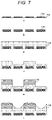
- FIG. 7 is a diagram showing an example of a process of manufacturing the light-emitting module according to the second embodiment of the present technology.
- FIG. 8 is a diagram showing an example of a schematic cross-sectional structure of a light-emitting module according to a third embodiment of the present technology.
- FIG. 9 is a diagram showing an example of a process of manufacturing the light-emitting module according to the third embodiment of the present technology.
- FIG. 10 is a diagram showing an example of a schematic cross-sectional structure of a light-emitting module according to a fourth embodiment of the present technology.
- FIG. 11 is a diagram showing an example of a process of manufacturing the light-emitting module according to the fourth embodiment of the present technology.
- FIG. 12 is a diagram showing an example of a schematic cross-sectional structure of a light-emitting module according to a fifth embodiment of the present technology.
- FIG. 13 is a diagram showing an example of a process of manufacturing the light-emitting module according to the fifth embodiment of the present technology.
- FIG. 14 is a diagram showing an example of a schematic cross-sectional structure of a light-emitting module according to a sixth embodiment of the present technology.
- FIG. 15 is a diagram showing an example of a process of manufacturing the light-emitting module according to the sixth embodiment of the present technology.
- FIG. 16 is a diagram showing an example of a schematic cross-sectional structure of a light-emitting module according to a seventh embodiment of the present technology.
- FIG. 17 is a diagram showing an example of a process of manufacturing the light-emitting module according to the seventh embodiment of the present technology.
- FIG. 18 is a diagram showing the appearance of a smartphone 401 as a first application example of the embodiments of the present technology.
- FIG. 19 is a diagram showing the appearance of a digital camera 411 viewed from the front (subject side), as a second application example of the embodiments of the present technology.
- FIG. 20 is a diagram showing the appearance of the digital camera 411 , viewed from the back, as the second application example of the embodiments of the present technology.
- FIG. 21 is a diagram showing the appearance of an HMD 431 as a third application example of the embodiments of the present technology.
- FIG. 1 is a diagram showing an example of an overall configuration of a display device 100 according to an embodiment of the present technology.
- the display device 100 includes, for example, a pixel array portion 102 and a drive unit that drives the pixel array portion 102 .
- the drive unit includes a horizontal selector 103 , a write scanner 104 , and a power source scanner 105 .
- the pixel array portion 102 includes a plurality of pixel circuits 101 arranged in a matrix.
- a power line DSL and a scanning line WSL are provided in such a way as to correspond to each row of the plurality of pixel circuits 101 .
- a signal line DTL is provided in such a way as to correspond to each column of the plurality of pixel circuits 101 .
- the write scanner 104 sequentially supplies a control signal to each of the scanning lines WSL to perform line-sequential scanning of the pixel circuits 101 line by line.
- the power source scanner 105 supplies a source voltage to each of the power lines DSL in accordance with the line-sequential scanning.
- the horizontal selector 103 supplies a signal potential of a signal serving as a video signal and a reference potential to the signal lines DTL arranged in columns, in accordance with the line-sequential scanning.
- FIG. 2 is a diagram showing an example of a circuit configuration of the pixel circuit 101 according to the embodiment of the present technology.
- the pixel circuit 101 includes, for example, a light-emitting element 14 such as an organic EL element, a sampling transistor 11 , a driving transistor 12 , and a holding capacitor 13 .
- the sampling transistor 11 has a gate connected to the corresponding scanning line WSL.
- One of a source and a drain of the sampling transistor 11 is connected to the corresponding signal line DTL, and the other of the source and the drain is connected to the gate of the driving transistor 12 .
- the driving transistor 12 has a source connected to the anode of the light-emitting element 14 , and a drain connected to the corresponding power line DSL.
- the cathode of the light-emitting element 14 is connected to a grounding wire 15 . Note that the grounding wire 15 is laid such that the grounding wire 15 is common to all the pixel circuits 101 .
- the holding capacitor 13 is connected to the source and gate of the driving transistor 12 while being located therebetween.
- the holding capacitor 13 holds the signal potential of a video signal supplied from the signal line DTL.
- FIG. 3 is a diagram showing an example of a schematic cross-sectional structure of a light-emitting module according to a first embodiment of the present technology.
- a pixel according to the first embodiment includes an electrode 110 , a light-emitting element 120 , a protective layer 130 , a color filter 142 for blue color, and an optical layer 150 .
- the electrode 110 is an anode electrode of the light-emitting element 120 .
- the electrode 110 may be, for example, a transparent electrode including metal, such as AlCu alloy or tin (Ti), or indium tin oxide (ITO), and the like.
- the light-emitting element 120 corresponds to the above-described light-emitting element 14 that converts an electric signal into an optical signal.
- the light-emitting element 120 may be, for example, an organic EL element.
- an organic layer is formed between a cathode electrode and the electrode 110 .
- the material of the cathode electrode may be, for example, a transparent electrode of MgAg alloy or indium tin oxide (ITO), and the like.
- the protective layer 130 is a barrier layer that covers the light-emitting element 120 so as to prevent deterioration of the light-emitting element 120 .
- the material of the protective layer 130 may be, for example, silicon nitride (SiN).
- the color filter 142 is a color changing member that changes the color of light from the light-emitting element 120 .
- the color filter 142 is formed as a result of, for example, mixing an organic material such as a photoresist with an organic pigment and performing photolithography.
- a cross section of a repeated portion of a white pixel and a blue pixel is shown, and the color filter 142 for blue color is disposed in such a way as to correspond to the light-emitting element 120 of the blue pixel. Meanwhile, no color filter is disposed at the position of the white pixel.
- the color filter 142 is an example of the color changing member described in the claims.
- the optical layer 150 is a layer that covers the color filter 142 and the protective layer 130 and condenses or scatters light with its curved shape. That is, the optical layer 150 is a barrier layer of the color filter 142 , and is also a layer that functions as lenses.
- the material of the optical layer 150 may be an acrylic photopolymerizable composition. Furthermore, tin oxide (TiO 2 ) particles may be mixed as filler so as to improve a refractive index and also enhance capping properties.
- the optical layer 150 is formed by spin-coating of these materials. Accordingly, a convex lens is formed at the position of the blue pixel where the color filter 142 is disposed, and a concave lens is formed at the position of the white pixel where the color filter 142 is not disposed.
- FIG. 4 is a diagram showing examples of optical characteristics of the light-emitting module according to the first embodiment of the present technology.
- light 612 from the light-emitting element 120 is changed in color to blue by the color filter 142 and emitted through the convex lens of the optical layer 150 .
- light 611 from the light-emitting element 120 is emitted through the concave lens of the optical layer 150 .
- FIG. 5 is a diagram showing an example of a process of manufacturing the light-emitting module according to the first embodiment of the present technology.
- the electrode 110 is formed on a substrate 190 as shown in “a” of FIG. 5 .
- This electrode 110 is formed by lithography. That is, the electrode 110 is formed as follows. Patterning is provided after formation of a film of material to be the electrode 110 , and masking with resist is performed. Then, unnecessary portions are removed by etching, and the resist of the mask is removed.
- the light-emitting element 120 is formed on the electrode 110 as shown in “b” of FIG. 5 .
- the light-emitting element 120 is formed by vapor deposition. That is, the light-emitting element 120 is formed by deposition of a thin film of material to be the light-emitting element 120 in a gas phase.
- the protective layer 130 is formed on the surface of the substrate on which the light-emitting element 120 has been formed.
- This protective layer 130 is formed by chemical vapor deposition (CVD).
- the color filter 142 is formed as shown in “d” of FIG. 5 .
- This color filter 142 is formed by lithography.
- the optical layer 150 is formed as shown in “e” of FIG. 5 .
- the optical layer 150 is formed by spin-coating of the material of the optical layer 150 . That is, a liquid material is applied while a wafer is rotated. Thus, the material is applied to the surface thereof by use of centrifugal force. As a result, there is formed a film in a curved shape in accordance with the unevenness of the surface.
- the optical layer 150 in a curved shape, which covers the color filter 142 and the protective layer 130 .
- the optical layer 150 is a barrier layer of the color filter 142 and also functions as lenses.
- the curvature of the concave shape of an optical layer 150 has been changed at the position of a white pixel. Note that the overall configuration of a display device 100 is similar to that in the first embodiment described above, and thus detailed description will be omitted.
- FIG. 6 is a diagram showing an example of a schematic cross-sectional structure of a light-emitting module according to the second embodiment of the present technology.
- a pixel according to the second embodiment includes an electrode 110 , a light-emitting element 120 , a protective layer 130 , a color filter 142 for blue color, and the optical layer 150 , as in the first embodiment described above.
- the protective layer 130 has a recess at the position of a white pixel, and is lower in height than the protective layer 130 at the position of a blue pixel. Therefore, the curved shape of the optical layer 150 formed thereon is different from that in the first embodiment described above.
- the curvature of the concave shape of the optical layer 150 at the position of the white pixel is larger than the curvature of the convex shape of the optical layer 150 at the position of the blue pixel. It is possible to improve the power (refractive power) of the optical layer 150 as a lens at the position of the white pixel by changing the curvature in this manner.
- FIG. 7 is a diagram showing an example of a process of manufacturing the light-emitting module according to the second embodiment of the present technology. Steps “a” to “c” of FIG. 7 are similar to those in the first embodiment described above.
- the protective layer 130 is partially removed at the position of the white pixel.
- This shape is formed as follows. For example, patterning is provided after formation of a film of silicon nitride (SiN), and masking with resist is performed. Then, the protective layer 130 is partially removed by dry etching at the position of the white pixel, and the resist of the mask is removed.
- SiN silicon nitride
- the color filter 142 is formed as shown in “e” of FIG. 7 .
- This color filter 142 is formed by lithography.
- the optical layer 150 is formed as shown in “f” of FIG. 7 .
- the optical layer 150 is formed by spin-coating of the material of the optical layer 150 .
- the height of the protective layer 130 is reduced at the position of the white pixel.
- the curvature of the concave shape of the optical layer 150 is larger than the curvature of the convex shape of the optical layer 150 at the position of the blue pixel.
- the second embodiment of the present technology it is possible to improve the power of the optical layer 150 as a lens by increasing the curvature of the concave shape of the optical layer 150 at the position of the white pixel.
- an antireflection film is formed on the surface of an optical layer 150 .
- the overall configuration of a display device 100 is similar to that in the first embodiment described above, and thus detailed description will be omitted.
- FIG. 8 is a diagram showing an example of a schematic cross-sectional structure of a light-emitting module according to the third embodiment of the present technology.
- a pixel according to the third embodiment includes an electrode 110 , a light-emitting element 120 , a protective layer 130 , a color filter 142 for blue color, and the optical layer 150 , as in the first embodiment described above.
- the pixel according to the third embodiment further includes an antireflection film 160 on the surface of the optical layer 150 .
- the antireflection film 160 is a film that covers the surface of the optical layer 150 , and is an antireflection coating that reduces reflectance at a predetermined wavelength. Thus, reflection of external light can be prevented, so that the performance of the display device 100 can be improved.
- FIG. 9 is a diagram showing an example of a process of manufacturing the light-emitting module according to the third embodiment of the present technology. Steps “a” to “e” of FIG. 9 are similar to those in the first embodiment described above.
- the antireflection film 160 is formed on the surface of the optical layer 150 .
- the antireflection film 160 is formed by chemical vapor deposition (CVD).
- the material of the antireflection film 160 may be, for example, silicon dioxide (SiO 2 ).
- reflection of external light can be prevented by formation of the antireflection film 160 on the surface of the optical layer 150 , so that the performance of the display device 100 can be improved.
- the convex shape of an optical layer 150 is formed to collectively cover a plurality of pixels. Note that the overall configuration of a display device 100 is similar to that in the first embodiment described above, and thus detailed description will be omitted.
- FIG. 10 is a diagram showing an example of a schematic cross-sectional structure of a light-emitting module according to the fourth embodiment of the present technology.
- a pixel according to the fourth embodiment includes an electrode 110 , a light-emitting element 120 , a protective layer 130 , color filters 142 to 144 , and the optical layer 150 . That is, the color filter 142 for blue color is disposed in such a way as to correspond to the light-emitting element 120 of a blue pixel, the color filter 143 for red color is disposed in such a way as to correspond to the light-emitting element 120 of a red pixel, and the color filter 144 for green color is disposed in such a way as to correspond to the light-emitting element 120 of a green pixel. Note that the color filters 142 to 144 are examples of the color changing member described in the claims.
- the color filters 142 to 144 are closely located. Therefore, the optical layer 150 is formed thereon in a convex shape such that the convex-shaped portion of the optical layer 150 collectively covers the color filters 142 to 144 . Meanwhile, a concave shape of the optical layer 150 is formed at the position of a white pixel, as in the first embodiment described above.
- FIG. 11 is a diagram showing an example of a process of manufacturing the light-emitting module according to the fourth embodiment of the present technology. Steps “a” to “c” of FIG. 7 are similar to those in the first embodiment described above.
- the color filters 142 to 144 are formed as shown in “d” of FIG. 11 . These color filters 142 to 144 are sequentially formed by lithography.
- the optical layer 150 is formed as shown in “e” of FIG. 5 .
- the optical layer 150 is formed by spin-coating of the material of the optical layer 150 .
- the convex shape of the optical layer 150 is formed to collectively cover the color filters 142 to 144 .
- the convex shape of the optical layer 150 is formed to collectively cover the color filters 142 to 144 . As a result, it is possible to improve the performance of the optical layer 150 as a lens in a case where a viewing angle is increased.
- the surface of a color filter is formed in a concave shape. Note that the overall configuration of a display device 100 is similar to that in the first embodiment described above, and thus detailed description will be omitted.
- FIG. 12 is a diagram showing an example of a schematic cross-sectional structure of a light-emitting module according to the fifth embodiment of the present technology.
- a pixel according to the fifth embodiment includes an electrode 110 , a light-emitting element 120 , a protective layer 130 , color filters 142 to 144 , and an optical layer 150 , as in the fourth embodiment described above.
- a partition 131 is provided between each adjacent pair of pixels, and the surfaces of the color filters 142 to 144 are formed in a concave shape.
- each of the color filters 142 to 144 refracts light from the front.
- optical performance is improved.
- the partition 131 reflects or absorbs light, and prevents light refracted by the concave shape of the surface of each of the color filters 142 to 144 from entering other pixels.
- FIG. 13 is a diagram showing an example of a process of manufacturing the light-emitting module according to the fifth embodiment of the present technology. Steps “a” to “c” of FIG. 7 are similar to those in the first embodiment described above.
- the protective layer 130 is partially removed at the position of each pixel to form the partitions 131 .
- This shape is formed as follows. For example, patterning is provided after formation of a film of silicon nitride (SiN), and masking with resist is performed. Then, the protective layer 130 is partially removed by dry etching at the position of the white pixel, and the resist of the mask is removed.
- the color filters 142 to 144 are formed at the respective positions of blue, red, and green colors divided by the partitions 131 . These color filters 142 to 144 are formed by sequential spin-coating of respective materials.
- the optical layer 150 is formed as shown in “f” of FIG. 7 .
- the optical layer 150 is formed by spin-coating of the material of the optical layer 150 .
- the convex shape of the optical layer 150 is formed to collectively cover the color filters 142 to 144 , as in the fourth embodiment described above.
- optical performance can be improved by the concave shape of the surface of each of the color filters 142 to 144 .
- the partition 131 can prevent light refracted by the concave shape from entering other pixels.
- color filters for some colors are different in thickness from the rest of color filters. Note that the overall configuration of a display device 100 is similar to that in the first embodiment described above, and thus detailed description will be omitted.
- FIG. 14 is a diagram showing an example of a schematic cross-sectional structure of a light-emitting module according to the sixth embodiment of the present technology.
- a pixel according to the sixth embodiment includes an electrode 110 , a light-emitting element 120 , a protective layer 130 , color filters 142 to 144 , and an optical layer 150 , as in the fourth embodiment described above.
- the color filter 144 for green color is formed such that the color filter 144 is thinner than the color filters 142 and 143 for the other colors. As a result, color balance can be adjusted.
- the optical layer 150 formed thereon has a concave shape at the position of the green pixel.
- FIG. 15 is a diagram showing an example of a process of manufacturing the light-emitting module according to the sixth embodiment of the present technology. Steps “a” to “c” of FIG. 7 are similar to those in the first embodiment described above.
- the color filters 142 to 144 are formed as shown in “d” of FIG. 11 . These color filters 142 to 144 are sequentially formed by lithography. In this case, the color filter 144 for green color is formed such that the color filter 144 is thinner than the color filters 142 and 143 for the other colors.
- the optical layer 150 is formed as shown in “e” of FIG. 5 .
- the optical layer 150 is formed by spin-coating of the material of the optical layer 150 .
- the convex shape of the optical layer 150 is formed to collectively cover the color filter 142 for blue color and the color filter 143 for red color.
- the concave shape of the optical layer 150 is formed on the color filter 144 for green color.
- the concave shape of the optical layer 150 is formed at the position of a white pixel.
- color filters 142 to 144 are arranged with gaps therebetween. Note that the overall configuration of a display device 100 is similar to that in the first embodiment described above, and thus detailed description will be omitted.
- FIG. 16 is a diagram showing an example of a schematic cross-sectional structure of a light-emitting module according to the seventh embodiment of the present technology.
- a pixel according to the seventh embodiment includes an electrode 110 , a light-emitting element 120 , a protective layer 130 , the color filters 142 to 144 , and an optical layer 150 , as in the fourth embodiment described above.
- the color filters 142 to 144 are arranged with gaps therebetween.
- the optical layer 150 is formed thereon such that the optical layer 150 has a convex shape separately at each pixel position.
- FIG. 17 is a diagram showing an example of a process of manufacturing the light-emitting module according to the seventh embodiment of the present technology. Steps “a” to “c” of FIG. 7 are similar to those in the first embodiment described above.
- the color filters 142 to 144 are formed as shown in “d” of FIG. 11 . These color filters 142 to 144 are sequentially formed by lithography. At this time, the color filters 142 to 144 are formed with gaps therebetween.
- the optical layer 150 is formed as shown in “e” of FIG. 5 .
- the optical layer 150 is formed by spin-coating of the material of the optical layer 150 .
- the convex shape of the optical layer 150 is separately formed at each of blue, red, and green pixel positions. Meanwhile, a concave shape is formed at the position of a white pixel.
- the convex shape of the optical layer 150 is separately formed at each of the blue, red, and green pixel positions. As a result, it is possible to provide the optical layer 150 formed in a convex shape at positions of pixels other than a white pixel, regardless of the disposition of the white pixel.
- FIG. 18 is a diagram showing the appearance of a smartphone 401 as a first application example of the embodiments of the present technology.
- the smartphone 401 includes an operation unit 403 and a display unit 405 .
- the operation unit 403 receives an operation input from a user.
- the display unit 405 displays various types of information.
- the display unit 405 may include any of the display devices according to the above-described embodiments.
- FIG. 19 is a diagram showing the appearance of a digital camera 411 viewed from the front (subject side), as a second application example of the embodiments of the present technology.
- FIG. 20 is a diagram showing the appearance of the digital camera 411 , viewed from the back, as the second application example of the embodiments of the present technology.
- the digital camera 411 includes a main body (camera body) 413 , an interchangeable lens unit 415 , and a grip portion 417 to be held by a user at the time of capturing an image.
- the digital camera 411 also includes a monitor 419 and an electronic viewfinder (EVF) 421 .
- the monitor 419 displays various types of information.
- the EVF 421 displays a through image to be viewed by the user at the time of capturing an image.
- the monitor 419 and the EVF 421 may include any of the display devices according to the above-described embodiments.
- FIG. 21 is a diagram showing the appearance of an HMD 431 as a third application example of the embodiments of the present technology.
- the head mounted display (HMD) 431 includes a spectacle-type display unit 433 and ear hook portions 435 .
- the display unit 433 displays various types of information.
- the ear hook portions 435 are hooked on a user's ears when the user wears the HMD 431 .
- the display unit 433 may include any of the display devices according to the above-described embodiments.
- the display device can be applied to a display device to be mounted on an electronic device of any field, such as a television device, an electronic book, a PDA, a notebook PC, a video camera, or a game device, that provides display on the basis of an image signal input from the outside or internally generated.
- a light-emitting module including:
- a protective layer that covers the light-emitting elements
- color changing members disposed in such a way as to correspond to at least some of the light-emitting elements with the protective layer interposed between the color changing members and the some of the light-emitting elements;
- an optical layer that covers the color changing members and the protective layer, and condenses or scatters light with a curved shape.
- the color changing members are not disposed at positions of white pixels, and
- a surface of the optical layer is formed in a concave shape at the positions of the white pixels.
- the color changing members are disposed at positions of pixels other than white pixels, and
- a surface of the optical layer is formed in a convex shape at the positions of the pixels other than the white pixels.
- the surface of the optical layer is formed in a convex shape at the positions of the pixels other than the white pixels in such a way as to collectively cover a plurality of the pixels other than the white pixels.
- the color changing members are disposed at positions of pixels other than white pixels, and are not disposed at positions of the white pixels, and
- the optical layer is formed in a concave shape at the positions of the white pixels, and is formed in a convex shape at the positions of the pixels other than the white pixels such that the concave shape and the convex shape have curvatures different from each other.
- the color changing members are disposed at positions of pixels other than white pixels, and are formed such that the color changing members disposed at positions of some pixels are thinner than the color changing members corresponding to other pixels, and
- a surface of the optical layer is formed in a concave shape at the positions of the some pixels.
- the optical layer includes a transparent material.
- the optical layer includes a material containing at least an inorganic material.
- a film that covers a surface of the optical layer, and reduces a reflectance at a predetermined wavelength.
- a display device including:
- a protective layer that covers the light-emitting elements
- color changing members disposed in such a way as to correspond to at least some of the light-emitting elements with the protective layer interposed between the color changing members and the some of the light-emitting elements;
- an optical layer that covers the color changing members and the protective layer, and condenses or scatters light with a curved shape.
- a method for manufacturing a light-emitting module including:
Landscapes
- Physics & Mathematics (AREA)
- Optics & Photonics (AREA)
- General Physics & Mathematics (AREA)
- Engineering & Computer Science (AREA)
- Theoretical Computer Science (AREA)
- Electroluminescent Light Sources (AREA)
- Optical Elements Other Than Lenses (AREA)
- Surface Treatment Of Optical Elements (AREA)
Abstract
Description
- 11 Sampling transistor
- 12 Driving transistor
- 13 Holding capacitor
- 14 Light-emitting element
- 15 Grounding wire
- 100 Display device
- 101 Pixel circuit
- 102 Pixel array portion
- 103 Horizontal selector
- 104 Write scanner
- 105 Power source scanner
- 110 Electrode
- 120 Light-emitting element
- 130 Protective layer
- 131 Partition
- 142 to 144 Color filter
- 150 Optical layer
- 160 Antireflection film
- 190 Substrate
Claims (12)
Applications Claiming Priority (4)
| Application Number | Priority Date | Filing Date | Title |
|---|---|---|---|
| JPJP2017-255091 | 2017-12-29 | ||
| JP2017255091 | 2017-12-29 | ||
| JP2017-255091 | 2017-12-29 | ||
| PCT/JP2018/043681 WO2019130956A1 (en) | 2017-12-29 | 2018-11-28 | Light emitting module, display device, and methods for manufacturing light emitting module and display device |
Publications (2)
| Publication Number | Publication Date |
|---|---|
| US20200395575A1 US20200395575A1 (en) | 2020-12-17 |
| US11437603B2 true US11437603B2 (en) | 2022-09-06 |
Family
ID=67063441
Family Applications (1)
| Application Number | Title | Priority Date | Filing Date |
|---|---|---|---|
| US16/956,907 Active 2039-06-01 US11437603B2 (en) | 2017-12-29 | 2018-11-28 | Light-emitting module, display device, and methods for manufacturing with color changing members disposed at non-white pixels |
Country Status (4)
| Country | Link |
|---|---|
| US (1) | US11437603B2 (en) |
| JP (1) | JP7204677B2 (en) |
| CN (1) | CN111492271B (en) |
| WO (1) | WO2019130956A1 (en) |
Families Citing this family (2)
| Publication number | Priority date | Publication date | Assignee | Title |
|---|---|---|---|---|
| CN112331150A (en) * | 2020-11-05 | 2021-02-05 | Tcl华星光电技术有限公司 | Display device and light-emitting panel |
| WO2023068227A1 (en) * | 2021-10-22 | 2023-04-27 | ソニーセミコンダクタソリューションズ株式会社 | Display device and electronic equipment |
Citations (19)
| Publication number | Priority date | Publication date | Assignee | Title |
|---|---|---|---|---|
| US20030071935A1 (en) * | 2001-05-31 | 2003-04-17 | Seiko Epson Corporation | EL device, EL display, EL illumination apparatus, liquid crystal apparatus using the EL illumination apparatus and electronic apparatus |
| US20030223121A1 (en) * | 2002-04-10 | 2003-12-04 | Toshihiro Otake | Mask, substrate with light reflecting film, method for forming light reflecting film, method for manufacturing electro-optical device, electro-optical device, and electronic apparatus |
| US20060186802A1 (en) * | 2005-02-24 | 2006-08-24 | Eastman Kodak Company | Oled device having improved light output |
| CN101075663A (en) | 2006-05-16 | 2007-11-21 | 精工爱普生株式会社 | Luminous device, method of manufacturing luminous device and electronic device |
| US20080164551A1 (en) | 2006-12-28 | 2008-07-10 | Young-Je Yun | Image sensor |
| US20090051283A1 (en) | 2007-08-21 | 2009-02-26 | Cok Ronald S | Led device having improved contrast |
| US20110076469A1 (en) * | 2009-09-30 | 2011-03-31 | Fujifilm Corporation | Manufacturing method of optical film, optical film manufactured by the manufacturing method, and polarizing plate and image display having the optical film |
| JP2013051428A (en) | 2003-10-28 | 2013-03-14 | Dow Corning Corp | Method including applying flat-top deposit of composition onto substrate |
| JP2013058447A (en) | 2011-09-09 | 2013-03-28 | Canon Inc | Organic el light-emitting device |
| JP2013149536A (en) | 2012-01-23 | 2013-08-01 | Canon Inc | Display device |
| JP2013251173A (en) | 2012-06-01 | 2013-12-12 | Canon Inc | Display device manufacturing method and display device |
| JP2013254610A (en) | 2012-06-06 | 2013-12-19 | Rohm Co Ltd | Organic el light emitting device and method for manufacturing the same |
| CN103828486A (en) | 2011-10-03 | 2014-05-28 | 索尼公司 | Display device and electronic device |
| CN104051475A (en) | 2013-03-14 | 2014-09-17 | 采钰科技股份有限公司 | Solid-state imaging element |
| US8976436B2 (en) * | 2012-01-19 | 2015-03-10 | Kenneth A. Dean | Controlled diffuse scattering for displays |
| US20150077966A1 (en) * | 2012-04-13 | 2015-03-19 | Sharp Kabushiki Kaisha | Light-scattering body, light-scattering body film, light-scattering body substrate, light-scattering body device, light-emitting device, display device, and illumination device |
| JP2015187635A (en) | 2014-03-26 | 2015-10-29 | 株式会社Joled | Color variation member, light-emitting device, display device, and electronic apparatus |
| JP2016118710A (en) | 2014-12-22 | 2016-06-30 | 大日本印刷株式会社 | Color filter and electronic paper |
| WO2017082429A1 (en) | 2015-11-13 | 2017-05-18 | 凸版印刷株式会社 | Solid-state imaging element and method for manufacturing same |
Family Cites Families (3)
| Publication number | Priority date | Publication date | Assignee | Title |
|---|---|---|---|---|
| TWI397175B (en) * | 2009-02-09 | 2013-05-21 | Sony Corp | Solid-state imaging device, camera, electronic device, and manufacturing method of solid-state imaging device |
| JP2013016272A (en) * | 2011-06-30 | 2013-01-24 | Canon Inc | Display device |
| KR101975309B1 (en) * | 2012-07-25 | 2019-09-11 | 삼성디스플레이 주식회사 | Organic light emitting display device and manufacturing method thereof |
-
2018
- 2018-11-28 WO PCT/JP2018/043681 patent/WO2019130956A1/en not_active Ceased
- 2018-11-28 JP JP2019562875A patent/JP7204677B2/en active Active
- 2018-11-28 CN CN201880082707.8A patent/CN111492271B/en not_active Expired - Fee Related
- 2018-11-28 US US16/956,907 patent/US11437603B2/en active Active
Patent Citations (21)
| Publication number | Priority date | Publication date | Assignee | Title |
|---|---|---|---|---|
| US20030071935A1 (en) * | 2001-05-31 | 2003-04-17 | Seiko Epson Corporation | EL device, EL display, EL illumination apparatus, liquid crystal apparatus using the EL illumination apparatus and electronic apparatus |
| US20030223121A1 (en) * | 2002-04-10 | 2003-12-04 | Toshihiro Otake | Mask, substrate with light reflecting film, method for forming light reflecting film, method for manufacturing electro-optical device, electro-optical device, and electronic apparatus |
| JP2013051428A (en) | 2003-10-28 | 2013-03-14 | Dow Corning Corp | Method including applying flat-top deposit of composition onto substrate |
| US20060186802A1 (en) * | 2005-02-24 | 2006-08-24 | Eastman Kodak Company | Oled device having improved light output |
| CN101075663A (en) | 2006-05-16 | 2007-11-21 | 精工爱普生株式会社 | Luminous device, method of manufacturing luminous device and electronic device |
| JP2007311046A (en) | 2006-05-16 | 2007-11-29 | Seiko Epson Corp | LIGHT EMITTING DEVICE, LIGHT EMITTING DEVICE MANUFACTURING METHOD, AND ELECTRONIC DEVICE |
| US20080164551A1 (en) | 2006-12-28 | 2008-07-10 | Young-Je Yun | Image sensor |
| US20090051283A1 (en) | 2007-08-21 | 2009-02-26 | Cok Ronald S | Led device having improved contrast |
| US20110076469A1 (en) * | 2009-09-30 | 2011-03-31 | Fujifilm Corporation | Manufacturing method of optical film, optical film manufactured by the manufacturing method, and polarizing plate and image display having the optical film |
| JP2013058447A (en) | 2011-09-09 | 2013-03-28 | Canon Inc | Organic el light-emitting device |
| CN103828486A (en) | 2011-10-03 | 2014-05-28 | 索尼公司 | Display device and electronic device |
| US8976436B2 (en) * | 2012-01-19 | 2015-03-10 | Kenneth A. Dean | Controlled diffuse scattering for displays |
| JP2013149536A (en) | 2012-01-23 | 2013-08-01 | Canon Inc | Display device |
| US20150077966A1 (en) * | 2012-04-13 | 2015-03-19 | Sharp Kabushiki Kaisha | Light-scattering body, light-scattering body film, light-scattering body substrate, light-scattering body device, light-emitting device, display device, and illumination device |
| JP2013251173A (en) | 2012-06-01 | 2013-12-12 | Canon Inc | Display device manufacturing method and display device |
| JP2013254610A (en) | 2012-06-06 | 2013-12-19 | Rohm Co Ltd | Organic el light emitting device and method for manufacturing the same |
| CN104051475A (en) | 2013-03-14 | 2014-09-17 | 采钰科技股份有限公司 | Solid-state imaging element |
| JP2014179577A (en) | 2013-03-14 | 2014-09-25 | Visera Technologies Company Ltd | Solid-state imaging device |
| JP2015187635A (en) | 2014-03-26 | 2015-10-29 | 株式会社Joled | Color variation member, light-emitting device, display device, and electronic apparatus |
| JP2016118710A (en) | 2014-12-22 | 2016-06-30 | 大日本印刷株式会社 | Color filter and electronic paper |
| WO2017082429A1 (en) | 2015-11-13 | 2017-05-18 | 凸版印刷株式会社 | Solid-state imaging element and method for manufacturing same |
Also Published As
| Publication number | Publication date |
|---|---|
| CN111492271A (en) | 2020-08-04 |
| WO2019130956A1 (en) | 2019-07-04 |
| JP7204677B2 (en) | 2023-01-16 |
| CN111492271B (en) | 2022-06-14 |
| US20200395575A1 (en) | 2020-12-17 |
| JPWO2019130956A1 (en) | 2020-12-24 |
Similar Documents
| Publication | Publication Date | Title |
|---|---|---|
| US11026301B2 (en) | Organic EL device, method of manufacturing organic EL device, and electronic apparatus | |
| JP7245220B2 (en) | Display device and manufacturing method thereof | |
| US11322555B2 (en) | Light-emitting device, display apparatus, and image pickup apparatus | |
| US12295223B2 (en) | Display panel and display apparatus including the same | |
| US12349536B2 (en) | Electro-optical device and electronic apparatus | |
| WO2016056364A1 (en) | Display device, display device manufacturing method, and electronic equipment | |
| US11974455B2 (en) | Display device and method of manufacturing the same | |
| CN113711088B (en) | Display device and electronic apparatus | |
| JP7691172B2 (en) | Display device and electronic device | |
| US11437603B2 (en) | Light-emitting module, display device, and methods for manufacturing with color changing members disposed at non-white pixels | |
| US20230320181A1 (en) | Display device and head mounted display device | |
| US20250031525A1 (en) | Display device and method of fabricating the same | |
| US20250089540A1 (en) | Display device, method for manufacturing the same, and electronic apparatus | |
| US20240268199A1 (en) | Display panel and method of manufacturing the same | |
| US20260026234A1 (en) | Electronic device including multi-layer electrodes | |
| US20240268155A1 (en) | Display device | |
| KR20230074370A (en) | Display Apparatus |
Legal Events
| Date | Code | Title | Description |
|---|---|---|---|
| FEPP | Fee payment procedure |
Free format text: ENTITY STATUS SET TO UNDISCOUNTED (ORIGINAL EVENT CODE: BIG.); ENTITY STATUS OF PATENT OWNER: LARGE ENTITY |
|
| STPP | Information on status: patent application and granting procedure in general |
Free format text: DOCKETED NEW CASE - READY FOR EXAMINATION |
|
| AS | Assignment |
Owner name: SONY SEMICONDUCTOR SOLUTIONS CORPORATION, JAPAN Free format text: ASSIGNMENT OF ASSIGNORS INTEREST;ASSIGNORS:MAEDA, KENSAKU;SHINYA, KIMIHIRO;YAMAMOTO, ATSUSHI;SIGNING DATES FROM 20200811 TO 20201006;REEL/FRAME:055425/0972 |
|
| STPP | Information on status: patent application and granting procedure in general |
Free format text: NON FINAL ACTION MAILED |
|
| STPP | Information on status: patent application and granting procedure in general |
Free format text: RESPONSE TO NON-FINAL OFFICE ACTION ENTERED AND FORWARDED TO EXAMINER |
|
| STPP | Information on status: patent application and granting procedure in general |
Free format text: NOTICE OF ALLOWANCE MAILED -- APPLICATION RECEIVED IN OFFICE OF PUBLICATIONS |
|
| STPP | Information on status: patent application and granting procedure in general |
Free format text: PUBLICATIONS -- ISSUE FEE PAYMENT VERIFIED |
|
| STCF | Information on status: patent grant |
Free format text: PATENTED CASE |
|
| MAFP | Maintenance fee payment |
Free format text: PAYMENT OF MAINTENANCE FEE, 4TH YEAR, LARGE ENTITY (ORIGINAL EVENT CODE: M1551); ENTITY STATUS OF PATENT OWNER: LARGE ENTITY Year of fee payment: 4 |