US11437455B2 - Display device and method of manufacturing the same - Google Patents
Display device and method of manufacturing the same Download PDFInfo
- Publication number
- US11437455B2 US11437455B2 US16/856,780 US202016856780A US11437455B2 US 11437455 B2 US11437455 B2 US 11437455B2 US 202016856780 A US202016856780 A US 202016856780A US 11437455 B2 US11437455 B2 US 11437455B2
- Authority
- US
- United States
- Prior art keywords
- region
- transistor
- wide band
- gap
- channel region
- Prior art date
- Legal status (The legal status is an assumption and is not a legal conclusion. Google has not performed a legal analysis and makes no representation as to the accuracy of the status listed.)
- Active, expires
Links
Images




Classifications
-
- H—ELECTRICITY
- H10—SEMICONDUCTOR DEVICES; ELECTRIC SOLID-STATE DEVICES NOT OTHERWISE PROVIDED FOR
- H10K—ORGANIC ELECTRIC SOLID-STATE DEVICES
- H10K59/00—Integrated devices, or assemblies of multiple devices, comprising at least one organic light-emitting element covered by group H10K50/00
- H10K59/10—OLED displays
- H10K59/12—Active-matrix OLED [AMOLED] displays
- H10K59/121—Active-matrix OLED [AMOLED] displays characterised by the geometry or disposition of pixel elements
- H10K59/1213—Active-matrix OLED [AMOLED] displays characterised by the geometry or disposition of pixel elements the pixel elements being TFTs
-
- H01L27/3262—
-
- G—PHYSICS
- G09—EDUCATION; CRYPTOGRAPHY; DISPLAY; ADVERTISING; SEALS
- G09G—ARRANGEMENTS OR CIRCUITS FOR CONTROL OF INDICATING DEVICES USING STATIC MEANS TO PRESENT VARIABLE INFORMATION
- G09G3/00—Control arrangements or circuits, of interest only in connection with visual indicators other than cathode-ray tubes
- G09G3/20—Control arrangements or circuits, of interest only in connection with visual indicators other than cathode-ray tubes for presentation of an assembly of a number of characters, e.g. a page, by composing the assembly by combination of individual elements arranged in a matrix no fixed position being assigned to or needed to be assigned to the individual characters or partial characters
- G09G3/22—Control arrangements or circuits, of interest only in connection with visual indicators other than cathode-ray tubes for presentation of an assembly of a number of characters, e.g. a page, by composing the assembly by combination of individual elements arranged in a matrix no fixed position being assigned to or needed to be assigned to the individual characters or partial characters using controlled light sources
- G09G3/30—Control arrangements or circuits, of interest only in connection with visual indicators other than cathode-ray tubes for presentation of an assembly of a number of characters, e.g. a page, by composing the assembly by combination of individual elements arranged in a matrix no fixed position being assigned to or needed to be assigned to the individual characters or partial characters using controlled light sources using electroluminescent panels
-
- G—PHYSICS
- G09—EDUCATION; CRYPTOGRAPHY; DISPLAY; ADVERTISING; SEALS
- G09G—ARRANGEMENTS OR CIRCUITS FOR CONTROL OF INDICATING DEVICES USING STATIC MEANS TO PRESENT VARIABLE INFORMATION
- G09G3/00—Control arrangements or circuits, of interest only in connection with visual indicators other than cathode-ray tubes
- G09G3/20—Control arrangements or circuits, of interest only in connection with visual indicators other than cathode-ray tubes for presentation of an assembly of a number of characters, e.g. a page, by composing the assembly by combination of individual elements arranged in a matrix no fixed position being assigned to or needed to be assigned to the individual characters or partial characters
- G09G3/22—Control arrangements or circuits, of interest only in connection with visual indicators other than cathode-ray tubes for presentation of an assembly of a number of characters, e.g. a page, by composing the assembly by combination of individual elements arranged in a matrix no fixed position being assigned to or needed to be assigned to the individual characters or partial characters using controlled light sources
- G09G3/30—Control arrangements or circuits, of interest only in connection with visual indicators other than cathode-ray tubes for presentation of an assembly of a number of characters, e.g. a page, by composing the assembly by combination of individual elements arranged in a matrix no fixed position being assigned to or needed to be assigned to the individual characters or partial characters using controlled light sources using electroluminescent panels
- G09G3/32—Control arrangements or circuits, of interest only in connection with visual indicators other than cathode-ray tubes for presentation of an assembly of a number of characters, e.g. a page, by composing the assembly by combination of individual elements arranged in a matrix no fixed position being assigned to or needed to be assigned to the individual characters or partial characters using controlled light sources using electroluminescent panels semiconductive, e.g. using light-emitting diodes [LED]
- G09G3/3208—Control arrangements or circuits, of interest only in connection with visual indicators other than cathode-ray tubes for presentation of an assembly of a number of characters, e.g. a page, by composing the assembly by combination of individual elements arranged in a matrix no fixed position being assigned to or needed to be assigned to the individual characters or partial characters using controlled light sources using electroluminescent panels semiconductive, e.g. using light-emitting diodes [LED] organic, e.g. using organic light-emitting diodes [OLED]
-
- G—PHYSICS
- G09—EDUCATION; CRYPTOGRAPHY; DISPLAY; ADVERTISING; SEALS
- G09G—ARRANGEMENTS OR CIRCUITS FOR CONTROL OF INDICATING DEVICES USING STATIC MEANS TO PRESENT VARIABLE INFORMATION
- G09G3/00—Control arrangements or circuits, of interest only in connection with visual indicators other than cathode-ray tubes
- G09G3/20—Control arrangements or circuits, of interest only in connection with visual indicators other than cathode-ray tubes for presentation of an assembly of a number of characters, e.g. a page, by composing the assembly by combination of individual elements arranged in a matrix no fixed position being assigned to or needed to be assigned to the individual characters or partial characters
- G09G3/22—Control arrangements or circuits, of interest only in connection with visual indicators other than cathode-ray tubes for presentation of an assembly of a number of characters, e.g. a page, by composing the assembly by combination of individual elements arranged in a matrix no fixed position being assigned to or needed to be assigned to the individual characters or partial characters using controlled light sources
- G09G3/30—Control arrangements or circuits, of interest only in connection with visual indicators other than cathode-ray tubes for presentation of an assembly of a number of characters, e.g. a page, by composing the assembly by combination of individual elements arranged in a matrix no fixed position being assigned to or needed to be assigned to the individual characters or partial characters using controlled light sources using electroluminescent panels
- G09G3/32—Control arrangements or circuits, of interest only in connection with visual indicators other than cathode-ray tubes for presentation of an assembly of a number of characters, e.g. a page, by composing the assembly by combination of individual elements arranged in a matrix no fixed position being assigned to or needed to be assigned to the individual characters or partial characters using controlled light sources using electroluminescent panels semiconductive, e.g. using light-emitting diodes [LED]
- G09G3/3208—Control arrangements or circuits, of interest only in connection with visual indicators other than cathode-ray tubes for presentation of an assembly of a number of characters, e.g. a page, by composing the assembly by combination of individual elements arranged in a matrix no fixed position being assigned to or needed to be assigned to the individual characters or partial characters using controlled light sources using electroluminescent panels semiconductive, e.g. using light-emitting diodes [LED] organic, e.g. using organic light-emitting diodes [OLED]
- G09G3/3225—Control arrangements or circuits, of interest only in connection with visual indicators other than cathode-ray tubes for presentation of an assembly of a number of characters, e.g. a page, by composing the assembly by combination of individual elements arranged in a matrix no fixed position being assigned to or needed to be assigned to the individual characters or partial characters using controlled light sources using electroluminescent panels semiconductive, e.g. using light-emitting diodes [LED] organic, e.g. using organic light-emitting diodes [OLED] using an active matrix
- G09G3/3233—Control arrangements or circuits, of interest only in connection with visual indicators other than cathode-ray tubes for presentation of an assembly of a number of characters, e.g. a page, by composing the assembly by combination of individual elements arranged in a matrix no fixed position being assigned to or needed to be assigned to the individual characters or partial characters using controlled light sources using electroluminescent panels semiconductive, e.g. using light-emitting diodes [LED] organic, e.g. using organic light-emitting diodes [OLED] using an active matrix with pixel circuitry controlling the current through the light-emitting element
-
- H—ELECTRICITY
- H10—SEMICONDUCTOR DEVICES; ELECTRIC SOLID-STATE DEVICES NOT OTHERWISE PROVIDED FOR
- H10D—INORGANIC ELECTRIC SEMICONDUCTOR DEVICES
- H10D62/00—Semiconductor bodies, or regions thereof, of devices having potential barriers
- H10D62/10—Shapes, relative sizes or dispositions of the regions of the semiconductor bodies; Shapes of the semiconductor bodies
- H10D62/102—Constructional design considerations for preventing surface leakage or controlling electric field concentration
- H10D62/112—Constructional design considerations for preventing surface leakage or controlling electric field concentration for preventing surface leakage due to surface inversion layers, e.g. by using channel stoppers
-
- H—ELECTRICITY
- H10—SEMICONDUCTOR DEVICES; ELECTRIC SOLID-STATE DEVICES NOT OTHERWISE PROVIDED FOR
- H10D—INORGANIC ELECTRIC SEMICONDUCTOR DEVICES
- H10D62/00—Semiconductor bodies, or regions thereof, of devices having potential barriers
- H10D62/40—Crystalline structures
- H10D62/402—Amorphous materials
-
- H—ELECTRICITY
- H10—SEMICONDUCTOR DEVICES; ELECTRIC SOLID-STATE DEVICES NOT OTHERWISE PROVIDED FOR
- H10D—INORGANIC ELECTRIC SEMICONDUCTOR DEVICES
- H10D62/00—Semiconductor bodies, or regions thereof, of devices having potential barriers
- H10D62/80—Semiconductor bodies, or regions thereof, of devices having potential barriers characterised by the materials
- H10D62/83—Semiconductor bodies, or regions thereof, of devices having potential barriers characterised by the materials being Group IV materials, e.g. B-doped Si or undoped Ge
-
- H—ELECTRICITY
- H10—SEMICONDUCTOR DEVICES; ELECTRIC SOLID-STATE DEVICES NOT OTHERWISE PROVIDED FOR
- H10D—INORGANIC ELECTRIC SEMICONDUCTOR DEVICES
- H10D86/00—Integrated devices formed in or on insulating or conducting substrates, e.g. formed in silicon-on-insulator [SOI] substrates or on stainless steel or glass substrates
- H10D86/40—Integrated devices formed in or on insulating or conducting substrates, e.g. formed in silicon-on-insulator [SOI] substrates or on stainless steel or glass substrates characterised by multiple TFTs
-
- H—ELECTRICITY
- H10—SEMICONDUCTOR DEVICES; ELECTRIC SOLID-STATE DEVICES NOT OTHERWISE PROVIDED FOR
- H10K—ORGANIC ELECTRIC SOLID-STATE DEVICES
- H10K59/00—Integrated devices, or assemblies of multiple devices, comprising at least one organic light-emitting element covered by group H10K50/00
- H10K59/10—OLED displays
- H10K59/12—Active-matrix OLED [AMOLED] displays
- H10K59/123—Connection of the pixel electrodes to the thin film transistors [TFT]
-
- G—PHYSICS
- G09—EDUCATION; CRYPTOGRAPHY; DISPLAY; ADVERTISING; SEALS
- G09G—ARRANGEMENTS OR CIRCUITS FOR CONTROL OF INDICATING DEVICES USING STATIC MEANS TO PRESENT VARIABLE INFORMATION
- G09G2300/00—Aspects of the constitution of display devices
- G09G2300/04—Structural and physical details of display devices
- G09G2300/0421—Structural details of the set of electrodes
- G09G2300/0426—Layout of electrodes and connections
-
- G—PHYSICS
- G09—EDUCATION; CRYPTOGRAPHY; DISPLAY; ADVERTISING; SEALS
- G09G—ARRANGEMENTS OR CIRCUITS FOR CONTROL OF INDICATING DEVICES USING STATIC MEANS TO PRESENT VARIABLE INFORMATION
- G09G2300/00—Aspects of the constitution of display devices
- G09G2300/08—Active matrix structure, i.e. with use of active elements, inclusive of non-linear two terminal elements, in the pixels together with light emitting or modulating elements
- G09G2300/0809—Several active elements per pixel in active matrix panels
-
- G—PHYSICS
- G09—EDUCATION; CRYPTOGRAPHY; DISPLAY; ADVERTISING; SEALS
- G09G—ARRANGEMENTS OR CIRCUITS FOR CONTROL OF INDICATING DEVICES USING STATIC MEANS TO PRESENT VARIABLE INFORMATION
- G09G2300/00—Aspects of the constitution of display devices
- G09G2300/08—Active matrix structure, i.e. with use of active elements, inclusive of non-linear two terminal elements, in the pixels together with light emitting or modulating elements
- G09G2300/0809—Several active elements per pixel in active matrix panels
- G09G2300/0819—Several active elements per pixel in active matrix panels used for counteracting undesired variations, e.g. feedback or autozeroing
-
- G—PHYSICS
- G09—EDUCATION; CRYPTOGRAPHY; DISPLAY; ADVERTISING; SEALS
- G09G—ARRANGEMENTS OR CIRCUITS FOR CONTROL OF INDICATING DEVICES USING STATIC MEANS TO PRESENT VARIABLE INFORMATION
- G09G2300/00—Aspects of the constitution of display devices
- G09G2300/08—Active matrix structure, i.e. with use of active elements, inclusive of non-linear two terminal elements, in the pixels together with light emitting or modulating elements
- G09G2300/0809—Several active elements per pixel in active matrix panels
- G09G2300/0842—Several active elements per pixel in active matrix panels forming a memory circuit, e.g. a dynamic memory with one capacitor
-
- G—PHYSICS
- G09—EDUCATION; CRYPTOGRAPHY; DISPLAY; ADVERTISING; SEALS
- G09G—ARRANGEMENTS OR CIRCUITS FOR CONTROL OF INDICATING DEVICES USING STATIC MEANS TO PRESENT VARIABLE INFORMATION
- G09G2300/00—Aspects of the constitution of display devices
- G09G2300/08—Active matrix structure, i.e. with use of active elements, inclusive of non-linear two terminal elements, in the pixels together with light emitting or modulating elements
- G09G2300/0809—Several active elements per pixel in active matrix panels
- G09G2300/0842—Several active elements per pixel in active matrix panels forming a memory circuit, e.g. a dynamic memory with one capacitor
- G09G2300/0861—Several active elements per pixel in active matrix panels forming a memory circuit, e.g. a dynamic memory with one capacitor with additional control of the display period without amending the charge stored in a pixel memory, e.g. by means of additional select electrodes
-
- G—PHYSICS
- G09—EDUCATION; CRYPTOGRAPHY; DISPLAY; ADVERTISING; SEALS
- G09G—ARRANGEMENTS OR CIRCUITS FOR CONTROL OF INDICATING DEVICES USING STATIC MEANS TO PRESENT VARIABLE INFORMATION
- G09G2310/00—Command of the display device
- G09G2310/02—Addressing, scanning or driving the display screen or processing steps related thereto
- G09G2310/0202—Addressing of scan or signal lines
- G09G2310/0216—Interleaved control phases for different scan lines in the same sub-field, e.g. initialization, addressing and sustaining in plasma displays that are not simultaneous for all scan lines
-
- G—PHYSICS
- G09—EDUCATION; CRYPTOGRAPHY; DISPLAY; ADVERTISING; SEALS
- G09G—ARRANGEMENTS OR CIRCUITS FOR CONTROL OF INDICATING DEVICES USING STATIC MEANS TO PRESENT VARIABLE INFORMATION
- G09G2320/00—Control of display operating conditions
- G09G2320/02—Improving the quality of display appearance
- G09G2320/0209—Crosstalk reduction, i.e. to reduce direct or indirect influences of signals directed to a certain pixel of the displayed image on other pixels of said image, inclusive of influences affecting pixels in different frames or fields or sub-images which constitute a same image, e.g. left and right images of a stereoscopic display
- G09G2320/0214—Crosstalk reduction, i.e. to reduce direct or indirect influences of signals directed to a certain pixel of the displayed image on other pixels of said image, inclusive of influences affecting pixels in different frames or fields or sub-images which constitute a same image, e.g. left and right images of a stereoscopic display with crosstalk due to leakage current of pixel switch in active matrix panels
-
- G—PHYSICS
- G09—EDUCATION; CRYPTOGRAPHY; DISPLAY; ADVERTISING; SEALS
- G09G—ARRANGEMENTS OR CIRCUITS FOR CONTROL OF INDICATING DEVICES USING STATIC MEANS TO PRESENT VARIABLE INFORMATION
- G09G2320/00—Control of display operating conditions
- G09G2320/02—Improving the quality of display appearance
- G09G2320/0233—Improving the luminance or brightness uniformity across the screen
-
- H01L2227/323—
-
- H01L27/1222—
-
- H01L27/1274—
-
- H01L27/1288—
-
- H01L29/66757—
-
- H01L29/78675—
-
- H01L29/78696—
-
- H—ELECTRICITY
- H10—SEMICONDUCTOR DEVICES; ELECTRIC SOLID-STATE DEVICES NOT OTHERWISE PROVIDED FOR
- H10D—INORGANIC ELECTRIC SEMICONDUCTOR DEVICES
- H10D30/00—Field-effect transistors [FET]
- H10D30/01—Manufacture or treatment
- H10D30/021—Manufacture or treatment of FETs having insulated gates [IGFET]
- H10D30/031—Manufacture or treatment of FETs having insulated gates [IGFET] of thin-film transistors [TFT]
- H10D30/0312—Manufacture or treatment of FETs having insulated gates [IGFET] of thin-film transistors [TFT] characterised by the gate electrodes
- H10D30/0314—Manufacture or treatment of FETs having insulated gates [IGFET] of thin-film transistors [TFT] characterised by the gate electrodes of lateral top-gate TFTs comprising only a single gate
-
- H—ELECTRICITY
- H10—SEMICONDUCTOR DEVICES; ELECTRIC SOLID-STATE DEVICES NOT OTHERWISE PROVIDED FOR
- H10D—INORGANIC ELECTRIC SEMICONDUCTOR DEVICES
- H10D30/00—Field-effect transistors [FET]
- H10D30/01—Manufacture or treatment
- H10D30/021—Manufacture or treatment of FETs having insulated gates [IGFET]
- H10D30/031—Manufacture or treatment of FETs having insulated gates [IGFET] of thin-film transistors [TFT]
- H10D30/0321—Manufacture or treatment of FETs having insulated gates [IGFET] of thin-film transistors [TFT] comprising silicon, e.g. amorphous silicon or polysilicon
-
- H—ELECTRICITY
- H10—SEMICONDUCTOR DEVICES; ELECTRIC SOLID-STATE DEVICES NOT OTHERWISE PROVIDED FOR
- H10D—INORGANIC ELECTRIC SEMICONDUCTOR DEVICES
- H10D30/00—Field-effect transistors [FET]
- H10D30/60—Insulated-gate field-effect transistors [IGFET]
- H10D30/67—Thin-film transistors [TFT]
- H10D30/6729—Thin-film transistors [TFT] characterised by the electrodes
- H10D30/673—Thin-film transistors [TFT] characterised by the electrodes characterised by the shapes, relative sizes or dispositions of the gate electrodes
- H10D30/6731—Top-gate only TFTs
-
- H—ELECTRICITY
- H10—SEMICONDUCTOR DEVICES; ELECTRIC SOLID-STATE DEVICES NOT OTHERWISE PROVIDED FOR
- H10D—INORGANIC ELECTRIC SEMICONDUCTOR DEVICES
- H10D30/00—Field-effect transistors [FET]
- H10D30/60—Insulated-gate field-effect transistors [IGFET]
- H10D30/67—Thin-film transistors [TFT]
- H10D30/6729—Thin-film transistors [TFT] characterised by the electrodes
- H10D30/673—Thin-film transistors [TFT] characterised by the electrodes characterised by the shapes, relative sizes or dispositions of the gate electrodes
- H10D30/6733—Multi-gate TFTs
-
- H—ELECTRICITY
- H10—SEMICONDUCTOR DEVICES; ELECTRIC SOLID-STATE DEVICES NOT OTHERWISE PROVIDED FOR
- H10D—INORGANIC ELECTRIC SEMICONDUCTOR DEVICES
- H10D30/00—Field-effect transistors [FET]
- H10D30/60—Insulated-gate field-effect transistors [IGFET]
- H10D30/67—Thin-film transistors [TFT]
- H10D30/674—Thin-film transistors [TFT] characterised by the active materials
- H10D30/6741—Group IV materials, e.g. germanium or silicon carbide
- H10D30/6743—Silicon
- H10D30/6745—Polycrystalline or microcrystalline silicon
-
- H—ELECTRICITY
- H10—SEMICONDUCTOR DEVICES; ELECTRIC SOLID-STATE DEVICES NOT OTHERWISE PROVIDED FOR
- H10D—INORGANIC ELECTRIC SEMICONDUCTOR DEVICES
- H10D30/00—Field-effect transistors [FET]
- H10D30/60—Insulated-gate field-effect transistors [IGFET]
- H10D30/67—Thin-film transistors [TFT]
- H10D30/6757—Thin-film transistors [TFT] characterised by the structure of the channel, e.g. transverse or longitudinal shape or doping profile
-
- H—ELECTRICITY
- H10—SEMICONDUCTOR DEVICES; ELECTRIC SOLID-STATE DEVICES NOT OTHERWISE PROVIDED FOR
- H10D—INORGANIC ELECTRIC SEMICONDUCTOR DEVICES
- H10D86/00—Integrated devices formed in or on insulating or conducting substrates, e.g. formed in silicon-on-insulator [SOI] substrates or on stainless steel or glass substrates
- H10D86/01—Manufacture or treatment
- H10D86/021—Manufacture or treatment of multiple TFTs
- H10D86/0221—Manufacture or treatment of multiple TFTs comprising manufacture, treatment or patterning of TFT semiconductor bodies
- H10D86/0223—Manufacture or treatment of multiple TFTs comprising manufacture, treatment or patterning of TFT semiconductor bodies comprising crystallisation of amorphous, microcrystalline or polycrystalline semiconductor materials
-
- H—ELECTRICITY
- H10—SEMICONDUCTOR DEVICES; ELECTRIC SOLID-STATE DEVICES NOT OTHERWISE PROVIDED FOR
- H10D—INORGANIC ELECTRIC SEMICONDUCTOR DEVICES
- H10D86/00—Integrated devices formed in or on insulating or conducting substrates, e.g. formed in silicon-on-insulator [SOI] substrates or on stainless steel or glass substrates
- H10D86/01—Manufacture or treatment
- H10D86/021—Manufacture or treatment of multiple TFTs
- H10D86/0231—Manufacture or treatment of multiple TFTs using masks, e.g. half-tone masks
-
- H—ELECTRICITY
- H10—SEMICONDUCTOR DEVICES; ELECTRIC SOLID-STATE DEVICES NOT OTHERWISE PROVIDED FOR
- H10D—INORGANIC ELECTRIC SEMICONDUCTOR DEVICES
- H10D86/00—Integrated devices formed in or on insulating or conducting substrates, e.g. formed in silicon-on-insulator [SOI] substrates or on stainless steel or glass substrates
- H10D86/40—Integrated devices formed in or on insulating or conducting substrates, e.g. formed in silicon-on-insulator [SOI] substrates or on stainless steel or glass substrates characterised by multiple TFTs
- H10D86/421—Integrated devices formed in or on insulating or conducting substrates, e.g. formed in silicon-on-insulator [SOI] substrates or on stainless steel or glass substrates characterised by multiple TFTs having a particular composition, shape or crystalline structure of the active layer
-
- H—ELECTRICITY
- H10—SEMICONDUCTOR DEVICES; ELECTRIC SOLID-STATE DEVICES NOT OTHERWISE PROVIDED FOR
- H10D—INORGANIC ELECTRIC SEMICONDUCTOR DEVICES
- H10D86/00—Integrated devices formed in or on insulating or conducting substrates, e.g. formed in silicon-on-insulator [SOI] substrates or on stainless steel or glass substrates
- H10D86/40—Integrated devices formed in or on insulating or conducting substrates, e.g. formed in silicon-on-insulator [SOI] substrates or on stainless steel or glass substrates characterised by multiple TFTs
- H10D86/60—Integrated devices formed in or on insulating or conducting substrates, e.g. formed in silicon-on-insulator [SOI] substrates or on stainless steel or glass substrates characterised by multiple TFTs wherein the TFTs are in active matrices
-
- H—ELECTRICITY
- H10—SEMICONDUCTOR DEVICES; ELECTRIC SOLID-STATE DEVICES NOT OTHERWISE PROVIDED FOR
- H10K—ORGANIC ELECTRIC SOLID-STATE DEVICES
- H10K59/00—Integrated devices, or assemblies of multiple devices, comprising at least one organic light-emitting element covered by group H10K50/00
- H10K59/10—OLED displays
- H10K59/12—Active-matrix OLED [AMOLED] displays
- H10K59/1201—Manufacture or treatment
Definitions
- disclosure relates to a display device and a method of manufacturing the same.
- Display devices display an image using pixels disposed in a display region.
- the pixels may be connected to scan lines and data lines and may include transistors.
- a pixel of an active light-emitting display device may include a light-emitting element, a driving transistor, and at least one switching transistor.
- a gate voltage of the driving transistor In order to express desired luminance in the pixels during an emission period of each frame, a gate voltage of the driving transistor should be maintained stable. However, due to the characteristics of transistors, a leakage current may occur in the pixel. The leakage current may cause a variation in gate voltage of the driving transistor, and in this case, desired luminance may not be sufficiently expressed in each pixel.
- this background of the technology section is, in part, intended to provide useful background for understanding the technology.
- this background of the technology section may also include ideas, concepts, or recognitions that were not part of what was known or appreciated by those skilled in the pertinent art prior to a corresponding effective filing date of the subject matter disclosed herein.
- An embodiment of the disclosure provides a display device capable of effectively reducing or preventing a leakage current of a pixel, and a method of manufacturing the same.
- a display device includes a pixel disposed in a display region.
- the pixel includes a light-emitting element connected between a first power source and a second power source; a first transistor connected between the first power source and the light-emitting element to control a driving current flowing in the light-emitting element in response to a voltage of a first node; and at least one switching transistor to transmit a data signal or a voltage of an initialization power source to the first node.
- the at least one switching transistor includes a first channel region, a first conductive region and a second conductive region which are respectively disposed at opposite sides of the first channel region, and a first wide band-gap region disposed between the first channel region and the second conductive region.
- the first channel region, the first conductive region, and the second conductive region may include polysilicon, and the first wide band-gap region may include amorphous silicon.
- the at least one switching transistor may include a plurality of transistors connected in series with each other.
- the at least one switching transistor may further include a second channel region disposed between the first channel region and the second conductive region, a third conductive region disposed between the first channel region and the second channel region, and a second wide band-gap region disposed between the second channel region and the third conductive region.
- the first wide band-gap region may be disposed between the first channel region and the third conductive region.
- the first wide band-gap region may be in direct contact with the first channel region and the third conductive region
- the second wide band-gap region may be in direct contact with the second channel region and the third conductive region
- the at least one switching transistor may include a first gate electrode overlapping the first channel region and a second gate electrode overlapping the second channel region.
- the first gate electrode and the second gate electrode may be electrically connected to each other.
- the at least one switching transistor may further include a second wide band-gap region disposed between the first channel region and the first conductive region.
- each of the first wide band-gap region and the second wide band-gap region may include amorphous silicon.
- the at least one switching transistor may include at least one of a second transistor connected between a first electrode of the first transistor and a data line the second transistor including a gate electrode connected to a scan line, a third transistor connected between a second electrode of the first transistor and the first node the third transistor including a gate electrode connected to the scan line, and a fourth transistor connected between the first node and the initialization power source and the fourth transistor including a gate electrode connected to a first control line.
- the third transistor may include the first channel region, the first conductive region, the second conductive region, and the first wide band-gap region.
- the third transistor may include a plurality of transistors connected in series with each other.
- the third transistor may further include a second channel region disposed between the first channel region and the second conductive region, a third conductive region disposed between the first channel region and the second channel region, and a second wide band-gap region disposed between the second channel region and the third conductive region.
- the first wide band-gap region may be disposed between the first channel region and the third conductive region.
- the third transistor may include a first gate electrode overlapping the first channel region and a second gate electrode overlapping the second channel region.
- the first gate electrode and the second gate electrode may be commonly connected to the scan line.
- the fourth transistor may include the first channel region, the first conductive region, the second conductive region, and the first wide band-gap region.
- the fourth transistor may include a plurality of transistors connected in series with each other.
- the second transistor may include the first channel region, the first conductive region, the second conductive region, the first wide band-gap region and a second wide band-gap region disposed between the first channel region and the first conductive region.
- the pixel may include a plurality of switching transistors, and a predetermined number of the switching transistors may include the first wide band-gap region.
- a method of manufacturing a display device including a switching transistor including forming a semiconductor pattern in a switching transistor region; disposing a first mask and a second mask on a first region and a second region, respectively, of the semiconductor pattern and exposing the remaining regions of the semiconductor pattern; crystallizing the remaining regions of the semiconductor pattern to include separating amorphous regions corresponding to the first and second regions and crystalline regions corresponding to the remaining regions; forming a first insulating film on the semiconductor pattern; forming a gate electrode on a region of the crystalline region; and doping another region of the crystalline region with impurities with the gate electrode as a mask.
- the switching transistor may include a plurality of transistors connected in series with each other.
- a region between channel regions of the transistors may be doped with impurities to form a conductive region, and the amorphous region may be formed between the conductive region and the channel regions.
- the switching transistor may be formed as a single transistor.
- the amorphous regions may be formed at opposite sides of the crystalline region overlapping the gate electrode.
- FIG. 1 illustrates a display device according to an embodiment.
- FIGS. 2 and 3 illustrate pixels PXL according to embodiments.
- FIGS. 4 and 5 illustrate a switching transistor according to an embodiment.
- FIGS. 6 and 7 illustrate a switching transistor according to an embodiment.
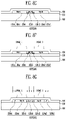
- FIGS. 8A to 8I illustrate a method of manufacturing a display device according to an embodiment and illustrates a method of manufacturing a switching transistor for the display device.
- FIG. 9 illustrates a pixel including a switching transistor according to an embodiment.
- FIG. 10 is a graph showing leakage current characteristics of switching transistors according to an embodiment.
- the phrase “in a plan view” means when an object portion is viewed from above
- the phrase “in a schematic cross-sectional view” means when a schematic cross-section taken by vertically cutting an object portion is viewed from the side.
- overlap or “overlapped” mean that a first object may be above or below or to a side of a second object, and vice versa. Additionally, the term “overlap” may include layer, stack, face or facing, extending over, covering or partly covering or any other suitable term as would be appreciated and understood by those of ordinary skill in the art.
- face and “facing” mean that a first element may directly or indirectly oppose a second element. In a case in which a third element intervenes between the first and second element, the first and second element may be understood as being indirectly opposed to one another, although still facing each other.
- a layer, film, region, substrate, or area When a layer, film, region, substrate, or area, is referred to as being “on” another layer, film, region, substrate, or area, it may be directly on the other film, region, substrate, or area, or intervening films, regions, substrates, or areas, may be present therebetween. Conversely, when a layer, film, region, substrate, or area, is referred to as being “directly on” another layer, film, region, substrate, or area, intervening layers, films, regions, substrates, or areas, may be absent therebetween.
- a layer, film, region, substrate, or area is referred to as being “below” another layer, film, region, substrate, or area, it may be directly below the other layer, film, region, substrate, or area, or intervening layers, films, regions, substrates, or areas, may be present therebetween. Conversely, when a layer, film, region, substrate, or area, is referred to as being “directly below” another layer, film, region, substrate, or area, intervening layers, films, regions, substrates, or areas, may be absent therebetween. Further, “over” or “on” may include positioning on or below an object and does not necessarily imply a direction based upon gravity.
- spatially relative terms “below”, “beneath”, “lower”, “above”, “upper”, or the like, may be used herein for ease of description to describe the relations between one element or component and another element or component as illustrated in the drawings. It will be understood that the spatially relative terms are intended to encompass different orientations of the device in use or operation, in addition to the orientation depicted in the drawings. For example, in the case where a device illustrated in the drawing is turned over, the device positioned “below” or “beneath” another device may be placed “above” another device. Accordingly, the illustrative term “below” may include both the lower and upper positions. The device may also be oriented in other directions and thus the spatially relative terms may be interpreted differently depending on the orientations.
- “About” or “approximately” as used herein is inclusive of the stated value and means within an acceptable range of deviation for the particular value as determined by one of ordinary skill in the art, considering the measurement in question and the error associated with measurement of the particular quantity (i.e., the limitations of the measurement system). For example, “about” may mean within one or more standard deviations, or within ⁇ 30%, 20%, 5% of the stated value.
- first and second are used to describe various elements, the elements are not limited by such terms. Such terms are merely used to differentiate one element from another element. Therefore, a first element mentioned below may also be a second element within the spirit and scope of the disclosure.
- the term “and/or” is intended to include any combination of the terms “and” and “or” for the purpose of its meaning and interpretation.
- “A and/or B” may be understood to mean “A, B, or A and B.”
- the terms “and” and “or” may be used in the conjunctive or disjunctive sense and may be understood to be equivalent to “and/or.”
- the phrase “at least one of” is intended to include the meaning of “at least one selected from the group of” for the purpose of its meaning and interpretation.
- “at least one of A and B” may be understood to mean “A, B, or A and B.”
- FIG. 1 illustrates a display device 1 according to an embodiment.
- FIG. 1 illustrates a light-emitting display device including light-emitting elements as an example of the display device 1
- the display device 1 according to the disclosure is not limited thereto.
- the display device 1 may include a display region 10 in which pixels PXL are disposed, a scan driver 20 to drive the pixels PXL, an emission control driver 30 , a data driver 40 , and a timing controller 50 .
- the display region 10 may include the pixels PXL connected to scan lines S 1 to Sn, emission control lines E 1 to En, and data lines D 1 to Dm.
- the “connection” may inclusively refer to electrical and/or physical connections.
- the pixels PXL may be electrically connected to the scan lines S 1 to Sn, the emission control lines E 1 to En, and the data lines D 1 to Dm.
- the emission control lines E 1 to En may be omitted.
- the structure and/or driving method of the pixels PXL may determine whether the emission control lines E 1 to En may be provided.
- the pixels PXL may be connected to at least one control line which is not shown. In this case, the operations of the pixels PXL may be controlled by a control signal supplied from the control line.
- the pixels PXL may receive scan signals, emission control signals (if applicable), and data signals from the scan lines S 1 to Sn, the emission control lines E 1 to En (if applicable), and the data lines D 1 to Dm.
- the pixels PXL may receive driving powers of a first power source ELVDD and a second power source ELVSS.
- the pixels PXL may be connected to other power sources (for example, initialization power source) according to the structure and/or driving method thereof of the pixels PXL.
- the above-described pixels PXL may receive the data signal from each of the data lines D 1 to Dm and emit light with luminance corresponding to the data signal. Accordingly, an image corresponding to the data signal of each frame may be displayed in the display region 10 .
- Each pixel PXL may include a light-emitting element and a pixel circuit for driving the light-emitting element.
- the pixel circuit may control a driving current flowing from the first power source ELVDD to the second power source ELVSS in response to a data signal.
- the pixel circuit may include a driving transistor and at least one switching transistor.
- the scan driver 20 may receive a scan driving control signal SCS from the timing controller 50 and supply scan signals to the scan lines S 1 to Sn in response to the scan driving control signal SCS. For example, the scan driver 20 may sequentially supply the scan signals to the scan lines S 1 to Sn in response to the scan driving control signal SCS. When the scan signals are supplied to the scan lines S 1 to Sn, the pixels PXL connected to the scan lines may be selected by the scan signals.
- the scan signals may be used to select the pixels PXL in a horizontal line unit.
- the scan signal may have a gate-on voltage (for example, a low voltage) by which a transistor of each of the pixels PXL connected to the data lines D 1 to Dm may be turned on.
- the scan signals may be supplied to the pixels PXL of a horizontal line corresponding to each horizontal period.
- the pixels PXL receiving the scan signals may be connected to the data lines D 1 to Dm to receive the data signals.
- the emission control driver 30 may receive an emission driving control signal ECS from the timing controller 50 and supply emission control signals to the emission control lines E 1 to En in response to the emission driving control signal ECS. In an example, the emission control driver 30 may sequentially supply the emission control signals to the emission control lines E 1 to En in response to the emission driving control signal ECS.
- the structure and/or driving method of the pixels PXL may determine whether the emission control driver 30 may be provided. Thus, the emission control driver 30 may be omitted.
- the emission control signal may be used to control an emission period (for example, an emission time point and/or an emission duration time) of the pixels PXL.
- the emission control signal may have a gate-off voltage (for example, a high voltage) by which at least one switching transistor positioned on a current path of each of the pixels PXL may be turned off.
- the pixel PXL receiving the emission control signal may be set to be in a non-emission state during a period in which the emission control signal is supplied and may be set to be in an emission state during other periods.
- the pixel PXL may maintain a non-emission state in response to the data signal even when the emission control signal having the gate-off voltage is not supplied.
- the data driver 40 may receive a data driving control signal DCS and image data RGB from the timing controller 50 and supply data signals to the data lines D 1 to Dm in response to the data driving control signal DCS and the image data RGB.
- the data signals supplied to the data lines D 1 to Dm may be supplied to the pixels PXL selected by the scan signals.
- the timing controller 50 may receive various timing control signals (for example, a vertical/horizontal synchronization signal and a main clock signal) from an external device (for example, a host processor) and may generate the scan driving control signal SCS, the emission driving control signal ECS, and the data driving control signal DCS in response to the timing control signals.
- the scan driving control signal SCS, the emission driving control signal ECS, and the data driving control signal DCS may be supplied to the scan driver 20 , the emission control driver 30 , and the data driver 40 , respectively.
- the scan driving control signal SCS may include a first start pulse (for example, a scan start pulse) and a first clock signal (for example, at least one scan clock signal).
- the first start pulse may be used to control an output timing of a first scan signal (for example, a scan signal supplied to a first scan line S 1 ).
- the first clock signal may be used to sequentially shift the first start pulses.
- the emission driving control signal ECS may include a second start pulse (for example, an emission start pulse) and a second clock signal (for example, at least one emission clock signal).
- the second start pulse may be used to control an output timing of a first emission control signal (for example, an emission control signal supplied to a first emission control line E 1 ).
- the second clock signal may be used to sequentially shift the second start pulses.
- the data driving control signal DCS may include a source sampling pulse, a source sampling clock, and a source output enable signal. A sampling operation of data may be controlled by the data driving control signal DCS.
- the timing controller 50 may receive input image data from the outside and may realign the input image data to generate the image data RGB.
- the above-described timing controller 50 may supply the image data RGB to the data driver 40 .
- the image data RGB supplied to the data driver 40 may be used to generate data signals to be supplied to the pixels PXL.
- FIGS. 2 and 3 illustrate pixels PXL according to embodiments.
- FIGS. 2 and 3 illustrate different embodiments of the pixel PXL that may be disposed in the display region 10 of FIG. 1 .
- the pixel PXL may be disposed in an i th pixel row (for example, an i th horizontal line) and a j th pixel column (for example, a j th vertical line) of the display region 10 and may be connected to an i th scan line Si, an i th emission control line Ei, and a j th data line Dj (wherein i and j are natural numbers).
- the pixel PXL may be connected to at least one control line.
- the pixel PXL may be connected to an i th first control line CL 1 i and an i th second control line CL 2 i.
- the pixels PXL disposed in the pixel region 10 of FIG. 1 may have substantially the same or similar structure.
- the “i th scan line Si,” the “i th emission control line Ei,” and the “j th data line Dj” will be respectively referred to as a “scan line Si”, an “emission control line Ei,” and a “data line Dj”.
- the “i th first control line CL 1 i ” and the “i th second control line CL 2 i ” will be respectively referred to as a “first control line CL 1 i ” and a “second control line CL 2 i.”
- the pixel PXL may include a light-emitting element EL and a pixel circuit PXC to drive the light-emitting element EL.
- the light-emitting element EL may be connected between the pixel circuit PXC and a second power source ELVSS, but the position of the light-emitting element EL is not limited thereto.
- the light-emitting element EL may be connected between a first power source ELVDD and the pixel circuit PXC.
- the light-emitting element EL may be an organic light-emitting diode (OLED) including an organic light-emitting layer but is not limited thereto.
- the pixel PXL may include micro light-emitting elements having a small size in a range of about a nanoscale to about a microscale.
- the light-emitting element EL may be connected between the first power source ELVDD and the second power source ELVSS.
- an anode electrode of the light-emitting element EL may be connected to the first power source ELVDD through the pixel circuit PXC, and a cathode electrode of the light-emitting element EL may be connected to the second power source ELVSS.
- a driving current is supplied from a first transistor T 1 , the light-emitting element EL generates light with luminance corresponding to the driving current.
- the first power source ELVDD and the second power source ELVSS may have a potential difference that allows the light-emitting element EL to emit light.
- the first power source ELVDD may be a high potential pixel power source
- the second power source ELVSS may be a low potential pixel power source having a potential that may be lower than that of the first power source ELVDD by a threshold voltage or more of the light-emitting element EL.
- the pixel circuit PXC may include a driving transistor, at least one switching transistor, and a storage capacitor Cst.
- the pixel circuit PXC may include a first transistor T 1 as the driving transistor, second to seventh transistors T 2 to T 7 as switching transistors, and the storage capacitor Cst.
- At least one switching transistor of the switching transistors may be provided to transmit a data signal or a voltage of an initialization power source to a first node N 1 to which a gate electrode of the driving transistor is connected.
- the structure of the pixel circuit PXC may be variously changed according to embodiments.
- the pixel PXL may include the pixel circuit PXC having various structures and/or driving methods.
- the assigning of the transistors (T 1 through T 7 ) as driving or switching transistors is arbitrary.
- the driving transistor may be any of the second to seventh transistors T 2 to T 7 and is thus not limited to the first transistor T 1 .
- the number of the transistors is not limited to that which is illustrated and may include any number of transistors within the spirt and scope of the disclosure.
- each of the first to seventh transistors T 1 to T 7 may be a p-type transistor.
- each of the first to seventh transistors T 1 to T 7 may be an n-type transistor.
- some of the first to seventh transistors T 1 to T 7 may be p-type transistors, and others thereof may be n-type transistors.
- the first transistor T 1 may be connected or disposed between the first power source ELVDD and the second power source ELVSS on a current path of a driving current.
- the first transistor T 1 may be connected or disposed between the first power source ELVDD and the light-emitting element EL.
- a first electrode (for example, a source electrode) of the first transistor T 1 may be connected to the first power source ELVDD through the fifth transistor T 5
- a second electrode (for example, a drain electrode) of the first transistor T 1 may be connected to the anode electrode of the light-emitting element EL through the sixth transistor T 6 .
- the gate electrode of the first transistor T 1 may be connected to the first node N 1 .
- the above-described first transistor T 1 controls a driving current flowing in the light-emitting element EL in response to a gate voltage, for example, a voltage of the first node N 1 .
- the first transistor T 1 may control a driving current flowing from the first power source ELVDD to the second power source ELVSS through the light-emitting element EL in response to the voltage of the first node N 1 .
- the second transistor T 2 may be connected or disposed between the data line Dj and the first electrode of the first transistor T 1 .
- a gate electrode of the second transistor T 2 may be connected to the scan line Si.
- the second transistor T 2 When a scan signal having a gate-on voltage is supplied to the scan line Si, the second transistor T 2 may be turned on to connect the data line Dj and the first electrode of the first transistor T 1 . Therefore, when the second transistor T 2 is turned on, a data signal from the data line Dj may be transmitted to the first electrode of the first transistor T 1 .
- the third transistor T 3 may also be turned on by the scan signal, and the first transistor T 1 may be turned on in the form of a diode connection by the third transistor T 3 .
- the data signal from the data line Dj may be transmitted to the first node N 1 through the second transistor T 2 , the first transistor T 1 , and the third transistor T 3 .
- the storage capacitor Cst may be charged with a voltage corresponding to the data signal and a threshold voltage of the first transistor T 1 .
- the third transistor T 3 may be connected or disposed between the second electrode of the first transistor T 1 and the first node N 1 .
- a gate electrode of the third transistor T 3 may be connected or disposed to the scan line Si.
- the third transistor T 3 may be turned on to connect the second electrode of the first transistor T 1 and the first node N 1 . Therefore, when the third transistor T 3 is turned on, the first transistor T 1 may be connected in the form of a diode.
- the fourth transistor T 4 may be connected or disposed between the first node N 1 and the initialization power source Vint.
- a gate electrode of the fourth transistor T 4 may be connected to the first control line CL 1 i .
- the first control line CL 1 i may be an initialization control line for initializing the pixels PXL of an i th horizontal line and may receive an initialization control signal having a gate-on voltage during an initialization period before a scan signal having a gate-on voltage is supplied to each scan line Si.
- the first control line CL 1 i may be any one scan line of previous scan lines for selecting the pixels PXL of previous horizontal lines, for example, an i th _ 1 scan line Si_ 1 for selecting the pixels PXL of an immediately previous horizontal line.
- the initialization control signal supplied to the first control line CL 1 i may be an (i ⁇ 1) th scan signal supplied to the (i ⁇ 1) th scan line Si ⁇ 1.
- the first control line CL 1 i may be a control line formed separately from scan lines S 1 to Sn of the pixels PXL.
- the fourth transistor T 4 When a first control signal having a gate-on voltage is supplied to the first control line CL 1 i , the fourth transistor T 4 may be turned on. When the fourth transistor T 4 is turned on, the voltage of the initialization power source Vint may be transmitted to the first node N 1 , and thus, the voltage of the first node N 1 may be initialized based on the voltage of the initialization power source Vint.
- the voltage of the initialization power source Vint may be set to a voltage less than or equal to a voltage of the data signal.
- the voltage of the initialization power source Vint may be set to be less than or equal to the lowest voltage of the data signal.
- the first transistor T 1 may be diode-connected in a forward direction during a scan period of each horizontal line (for example, a period in which the scan signal is supplied to each scan line Si) irrespective of a data signal of a previous frame. Accordingly, irrespective of the data signal of the previous frame, it may be possible to stably transmit the data signal of the current frame to the first node N 1 .
- the fifth transistor T 5 may be connected or disposed between the first power source ELVDD and the first transistor T 1 .
- a gate electrode of the fifth transistor T 5 may be connected to the emission control line Ei.
- the fifth transistor T 5 may be turned off when an emission control signal having a gate-off voltage is supplied to the emission control line Ei, and is turned on otherwise.
- the sixth transistor T 6 may be connected or disposed between the first transistor T 1 and the light-emitting element EL.
- a gate electrode of the sixth transistor T 6 may be connected to the emission control line Ei.
- the sixth transistor T 6 may be turned off when an emission control signal having a gate-off voltage is supplied to the emission control line Ei, and may be turned on otherwise.
- the fifth and sixth transistors T 5 and T 6 may be turned on or turned off at the same time in response to the emission control signal to control an emission period of the pixels PXL.
- the fifth and sixth transistors T 5 and T 6 are turned on, a current path through which a driving current flows may be formed in the pixel PXL. Accordingly, the pixel PXL may emit light with luminance corresponding to the voltage of the first node N 1 .
- the fifth and sixth transistors T 5 and T 6 are turned off, the current path may be blocked, and thus, the pixel PXL may not emit light.
- an emission control signal may be supplied as a signal having a gate-off voltage to turn off the fifth and sixth transistors T 5 and T 6 during an initialization period and a data programming period (for example, a scan period) of the pixel PXL.
- a data programming period for example, a scan period
- an emission control signal having a gate-off voltage may be supplied to overlap the scan signal, the first control signal, and the second control signal.
- a voltage of the emission control signal may be changed into a gate-on voltage, and thus, an emission period of each frame may start. Accordingly, the data signal may be stably stored in the pixel PXL prior to an emission period of each frame.
- the seventh transistor T 7 may be connected or disposed between the initialization power source Vint and the anode electrode of the light-emitting element EL.
- a gate electrode of the seventh transistor T 7 may be connected to the second control line CL 2 i .
- the second control line CL 2 i may be a bypass control line for initializing a voltage charged in an organic capacitor (for example, a parasitic capacitor formed due to the structure of the light-emitting element EL) formed in the light-emitting element EL of each of the pixels positioned in the i th horizontal line.
- the second control line CL 2 i may receive a bypass control signal having a gate-on voltage before each emission period.
- the second control line CL 2 i may be any one scan line of subsequent scan lines for selecting the pixels PXL of the subsequent horizontal lines.
- the second control line CL 2 i may be an (i+1) th scan line Si+1 for selecting the pixels PXL of an (i+1) th horizontal line but is not limited thereto.
- the second control line CL 2 i may be a current scan line (for example, the scan line Si) of each pixel PXL or may be a control line formed separately from the scan lines S 1 to Sn of the pixels PXL.
- the seventh transistor T 7 may be turned on to supply the voltage of the initialization power source Vint to the anode electrode of the light-emitting element EL. Therefore, the pixel PXL may exhibit more uniform luminance characteristics in response to each data signal.
- the storage capacitor Cst may be connected to the first power source ELVDD and the first node N 1 .
- the above-described storage capacitor Cst may be charged with a voltage corresponding to a data signal and a threshold voltage of the first transistor T 1 .
- each pixel PXL may include transistors including a driving transistor (for example, the first transistor T 1 ) and at least one switching transistor (for example, at least one of the second to seventh transistors T 2 to T 7 ).
- the transistors may be formed as transistors having similar structures, sizes, and/or types.
- at least one of the transistors may be formed as a transistor having a structure, size, and/or type which may be different from those of the remaining transistors.
- the driving transistor may have a relatively long channel region in order to secure an operation section in a wider voltage range.
- the driving transistor may be formed as a long-channel transistor.
- Each switching transistor may have a channel region relatively shorter than that of the driving transistor in order to efficiently utilize a limited pixel region while ensuring faster operating characteristics.
- Each switching transistor may be formed as a short-channel transistor.
- a leakage current occurring in the switching transistor may be increased to cause a variation in luminance of the pixel PXL.
- At least one switching transistor may include transistors connected in series with each other.
- each of third and fourth transistors T 3 and T 4 which are capable of changing a voltage of a first node N 1 when a leakage current occurs in an off-state, may be formed to include transistors connected in series with each other.
- each of the third transistor T 3 and the fourth transistor T 4 may be formed as a transistor with a dual structure including two transistors connected in series.
- the third transistor T 3 may include two transistors such as a 3 th _1 transistor T 3 _ 1 and a 3 th _2 transistor T 3 _ 2 connected in series between the first node N 1 and a second electrode of a first transistor T 1 .
- Gate electrodes of the 3 th _1 transistor T 3 _ 1 and the 3 th _2 transistor T 3 _ 2 may be commonly connected to the scan line Si. Accordingly, the 3 th _1 transistor T 3 _ 1 and the 3 th _2 transistor T 3 _ 2 may be turned on or off at the same time in response to a scan signal.
- the fourth transistor T 4 may include two transistors such as a 4 th _1 transistor T 4 _ 1 and a 4 th _2 transistor T 4 _ 2 connected in series between the first node N 1 and an initialization power source Vint. Gate electrodes of the 4 th _1 transistor T 4 _ 1 and the 4 th _2 transistor T 4 _ 2 may be commonly connected to the first control line CL 1 i . Accordingly, the 4 th _1 transistor T 4 _ 1 and the 4 th _2 transistor T 4 _ 2 may be turned on or off at the same time in response to a first control signal (for example, a previous scan signal).
- a first control signal for example, a previous scan signal.
- the third transistor T 3 and the fourth transistor T 4 are provided as a multiple-transistor having at least a dual structure, a leakage current of each of the third transistor T 3 and the fourth transistor T 4 may be reduced or prevented.
- it may be possible to reduce or prevent the leakage current through the third transistor T 3 and the fourth transistor T 4 in an off-state during an emission period of each frame, thereby stably maintaining the voltage of the first node N 1 . Accordingly, an expression of a gray level of the pixel PXL may be increased, and image quality of the display device 1 may be improved.
- FIG. 3 illustrates an embodiment in which each of the third and fourth transistors T 3 and T 4 is provided as the transistor with the dual structure, but the disclosure is not limited thereto.
- the third transistor T 3 and the fourth transistor T 4 only one transistor (for example, the third transistor T 3 ) may be formed as a transistor with a multi-structure, and the other transistor (for example, the fourth transistor T 4 ) may be formed as a transistor with a single structure.
- a switching transistor other than the third transistor T 3 and the fourth transistor T 4 for example, at least one transistor (for example, at least one transistor of a second transistor T 2 and fifth to seventh transistors T 5 to T 7 may also be formed as a transistor with a multi-structure including transistors connected in series with each other.
- the pixel PXL and the display device 1 including the pixel PXL may be possible to reduce or decrease a variation in gate voltage of the first transistor T 1 , for example, the voltage of the first node N 1 , which is caused by a leakage current. Accordingly, the pixel PXL may more accurately express a gray level corresponding to each data signal during each emission period.
- the structure of the pixel PXL is not limited to the embodiments shown in FIGS. 2 and 3 .
- the pixel PXL may include the pixel circuit PXC having various structures and/or driving methods within the spirit and scope of the disclosure.
- each transistor may be illustrated as being a p-type transistor, but the disclosure is not limited thereto.
- at least one transistor of the first to seventh transistors T 1 to T 7 may be an n-type transistor.
- a gate-on voltage for turning on the n-type transistor may be a high voltage.
- a voltage of a data signal may be determined according to the type of the first transistor T 1 .
- the first transistor T 1 is a p-type transistor, as a gray level to be expressed becomes higher, a data signal having a lower voltage may be supplied to each pixel PXL.
- the first transistor T 1 is an n-type transistor, as a gray level to be expressed becomes higher, a data signal having a higher voltage may be supplied to each pixel PXL.
- the types of the transistors constituting the pixel PXL and the voltage levels of various control signals for example, a scan signal, a data signal, a first control signal, a second control signal, and/or an emission control signal
- various control signals for example, a scan signal, a data signal, a first control signal, a second control signal, and/or an emission control signal
- FIGS. 4 and 5 illustrate a switching transistor Ts according to an embodiment.
- FIG. 4 illustrates a schematic cross-sectional structure of the switching transistor Ts
- FIG. 5 illustrates an equivalent circuit diagram of the switching transistor Ts.
- the switching transistor Ts according to the embodiment of FIGS. 4 and 5 may be any one switching transistor provided in the pixel PXL according to the embodiments of FIGS. 1 to 3 .
- the switching transistor Ts may be the third transistor T 3 with a dual structure according to the embodiment of FIG. 3 .
- the switching transistor Ts may include an active layer pattern 120 which may be disposed on one surface of a base layer 100 on which a buffer layer 110 may be formed, a gate electrode 140 which overlaps one region of the active layer pattern 120 with a first insulating film 130 interposed therebetween, first and second electrodes 160 and 170 which are spaced apart from the active layer pattern 120 with the first insulating film 130 and a second insulating film 150 interposed therebetween and are connected to different regions of the active layer pattern 120 .
- the switching transistor Ts may include a first switching transistor Ts_ 1 and a second switching transistor Ts_ 2 connected in series with each other.
- the first switching transistor Ts_ 1 and the second switching transistor Ts_ 2 may be the 3th_1 transistor T 3 _ 1 and the 3th_2 transistor T 3 _ 2 shown in FIG. 3 .
- the switching transistor Ts may include channel regions.
- the switching transistor Ts may include a first channel region 120 a 1 that forms a channel of the first switching transistor Ts_ 1 and a second channel region 120 a 2 that forms a channel of the second switching transistor Ts_ 2 .
- a conductive region may be disposed at each of opposite sides of each of the first channel region 120 a 1 and the second channel region 120 a 2 .
- a first conductive region 120 b 1 and a third conductive region 120 b 3 may be respectively disposed at opposite sides of the first channel region 120 a 1 .
- One of the first conductive region 120 b 1 and the third conductive region 120 b 3 may be a source region of the first switching transistor Ts_ 1 , and the other thereof may be a drain region of the first switching transistor Ts_ 1 .
- the third conductive region 120 b 3 may be the drain region of the first switching transistor Ts_ 1 .
- the third conductive region 120 b 3 may be the source region of the first switching transistor Ts_ 1 .
- This may be changed according to a carrier type (for example, an n-type or p-type) and a current direction of the first switching transistor Ts_ 1 .
- a second conductive region 120 b 2 and the third conductive region 120 b 3 may be respectively disposed at opposite sides of the second channel region 120 a 2 .
- One of the second conductive region 120 b 2 and the third conductive region 120 b 3 may be a source region of the second switching transistor Ts_ 2 , and the other thereof may be a drain region of the second switching transistor Ts_ 2 .
- the third conductive region 120 b 3 may be the source region of the second switching transistor Ts_ 2 .
- the third conductive region 120 b 3 may be the drain region of the second switching transistor Ts_ 2 .
- This may be changed according to a carrier type (for example, an n-type or p-type) and a current direction of the second switching transistor Ts_ 2 .
- the first switching transistor Ts_ 1 and the second switching transistor Ts_ 2 may share any one conductive region.
- the first switching transistor Ts_ 1 and the second switching transistor Ts_ 2 may share the third conductive region 120 b 3 .
- the disclosure is not limited thereto.
- the conductive regions of the first switching transistor Ts_ 1 and the second switching transistor Ts_ 2 may be formed in patterns separated apart from each other, and any conductive regions of the first and second switching transistors Ts_ 1 and Ts_ 2 (for example, the source region of the first switching transistor Ts_ 1 and the drain region of the second switching transistor Ts_ 2 ) may be electrically connected to each other.
- the switching transistor Ts may include at least one wide band-gap region.
- the switching transistor Ts may include a first wide band-gap region 120 c 1 disposed at one side of the first channel region 120 a 1 and a second wide band-gap region 120 c 2 disposed at one side of the second channel region 120 a 2 .
- the first wide band-gap region 120 c 1 and the second wide band-gap region 120 c 2 may be positioned between the first channel region 120 a 1 and the second channel region 120 a 2 .
- the first wide band-gap region 120 c 1 may be disposed between the first channel region 120 a 1 and the third conductive region 120 b 3
- the second wide band-gap region 120 c 2 may be disposed between the second channel region 120 a 2 and the third conductive region 120 b 3 .
- the switching transistor Ts may include at least one channel region, at least two conductive regions respectively disposed at opposite sides of the channel region, and at least one wide band-gap region disposed between the channel region and any one of the conductive regions.
- the switching transistor Ts may include at least one additional channel region, at least one conductive region, and at least one wide band-gap region.
- the switching transistor Ts may include the first channel region 120 a 1 , the first conductive region 120 b 1 and the third conductive region 120 b 3 which are respectively disposed at opposite sides of the first channel region 120 a 1 , and the first wide band-gap region 120 c 1 which is disposed between the first channel region 120 a 1 and the third conductive region 120 b 3 .
- the switching transistor Ts may include the second channel region 120 a 2 disposed between the first channel region 120 a 1 and the second conductive region 120 b 2 , the third conductive region 120 b 3 which may be disposed between the first channel region 120 a 1 and the second channel region 120 b 1 , and the second wide band-gap region 120 c 2 which may be disposed between the second channel region 120 a 2 and the third conductive region 120 b 3 .
- the first wide band-gap region 120 c 1 may be disposed between the first channel region 120 a 1 and the third conductive region 120 b 3 .
- the first and second wide band-gap regions 120 c 1 and 120 c 2 may be respectively disposed at opposite sides of the third conductive region 120 b 3 .
- the first wide band-gap region 120 c 1 may be disposed between the first channel region 120 a 1 and the third conductive region 120 b 3 to be in direct contact with the first channel region 120 a 1 and the third conductive region 120 b 3 .
- the second wide band-gap region 120 c 2 may be disposed between the second channel region 120 a 2 and the third conductive region 120 b 3 to be in direct contact with the second channel region 120 a 2 and the third conductive region 120 b 3 .
- the active layer pattern 120 may include a conductive region, a channel region, a wide band gap region, a conductive region, a wide band gap region, a channel region and a conductive region in symmetrical sequence in a schematic cross-sectional view as illustrated for example in FIG. 4 .
- the active layer pattern 120 of the switching transistor Ts may include the first conductive region 120 b 1 , the first channel region 120 a 1 , the first wide band-gap region 120 c 1 , the third conductive region 120 b 3 , the second wide band-gap region 120 c 2 , the second channel region 120 a 2 , and the second conductive region 120 b 2 , which are sequentially disposed in one direction on the buffer layer 110 as described above.
- the first conductive region 120 b 1 , the first channel region 120 a 1 , the first wide band-gap region 120 c 1 , and the third conductive region 120 b 3 may constitute an active layer pattern of the first switching transistor Ts_ 1 .
- the second conductive region 120 b 2 , the second channel region 120 a 2 , the second wide band-gap region 120 c 2 , and the third conductive region 120 b 3 may constitute an active layer pattern of the second switching transistor Ts_ 2 .
- the active layer patterns of the first and second switching transistors Ts_ 1 and Ts_ 2 may share the third conductive region 120 b 3 and may be integrally formed with each other.
- the active layer pattern 120 may have a relatively wide band-gap in the first and second wide band-gap regions 120 c 1 and 120 c 2 and may have a relatively low band-gap in the remaining regions.
- each of the first and second wide band-gap regions 120 c 1 and 120 c 2 may be an amorphous silicon region including amorphous silicon a-Si.
- Each of the first and second channel regions 120 a 1 and 120 a 2 and the first to third conductive regions 120 b 1 to 120 b 3 may be a polysilicon region including polysilicon poly-Si.
- the switching transistor Ts may include the gate electrode 140 with a dual structure.
- the gate electrode 140 may include a first gate electrode 140 a 1 overlapping the first channel region 120 a 1 and a second gate electrode 140 a 2 overlapping the second channel region 120 a 2 .
- the switching transistor Ts may include three or more channel regions and three or more gate electrodes overlapping with the channel regions.
- the gate electrode 140 may include multiple layers.
- the first gate electrode 140 a 1 may include multiple layers including a lower electrode 140 a 1 _ 1 disposed between the first insulating film 130 and the second insulating film 150 and an upper electrode 140 a 1 _ 2 connected to the lower electrode 140 a 1 _ 1 and disposed on the second insulating film 150 .
- the second gate electrode 140 a 2 may include multiple layers including a lower electrode 140 a 2 _ 1 disposed between the first insulating film 130 and the second insulating film 150 and an upper electrode 140 a 2 _ 2 connected to the lower electrode 140 a 2 _ 1 and disposed on the second insulating film 150 .
- resistance of the gate electrode 140 and a gate control line GC for example, the scan line Si
- one of the first gate electrode 140 a 1 and the second gate electrode 140 a 2 may include multiple layers, and the other thereof may include a single layer.
- each of the first gate electrode 140 a 1 and the second gate electrode 140 a 2 may include a single layer, and the first gate electrode 140 a 1 and the second gate electrode 140 a 2 may be disposed in the same layer or different layers.
- each of the first gate electrode 140 a 1 and the second gate electrode 140 a 2 may also include the lower electrodes 140 a 1 _ 1 and 140 a 2 _ 1 positioned between the first insulating film 130 and the second insulating film 150 or only the lower electrodes 140 a 1 _ 1 and 140 a 2 _ 1 positioned between the first insulating film 130 and the second insulating film 150 .
- the first gate electrode 140 a 1 and the second gate electrode 140 a 2 are electrically connected to each other.
- the first gate electrode 140 a 1 and the second gate electrode 140 a 2 may be connected to the same gate control line GC.
- the switching transistor Ts is the third transistor T 3 of FIG. 3
- the first gate electrode 140 a 1 and the second gate electrode 140 a 2 may be commonly connected to the scan line Si.
- the first electrode 160 and the second electrode 170 may be disposed on the second insulating film 150 to be connected to different regions of the active layer pattern 120 .
- the first electrode 160 may be connected to the first conductive region 120 b 1 through a first contact hole passing through the first and second insulating films 130 and 150
- the second electrode 170 may be connected to the second conductive region 120 b 2 through a second contact hole passing through the first and second insulating films 130 and 150 .
- the first electrode 160 may be one electrode of a source electrode and a drain electrode of the switching transistor Ts, and the second electrode 170 may be the other electrode thereof.
- the second electrode 170 may be the drain electrode.
- the second electrode 170 may be the source electrode.
- the position of the first electrode 160 and the second electrode 170 in the disclosure is not particularly limited and may be variously changed according to embodiments.
- at least one electrode of the first electrode 160 and the second electrode 170 may be omitted.
- the switching transistor Ts when the switching transistor Ts is connected directly to another circuit element (for example, at least one other transistor and/or capacitor) through the first conductive region 120 b 1 , the first electrode 160 may be omitted.
- the first conductive region 120 b 1 may be the source or drain electrode of the switching transistor Ts.
- the second electrode 170 when the switching transistor Ts is connected directly to another circuit element through the second conductive region 120 b 2 , the second electrode 170 may be omitted.
- the second conductive region 120 b 2 may be the source or drain electrode of the switching transistor Ts.
- first and/or second conductive regions 120 b 1 and 120 b 2 may be considered as the source and/or drain electrodes of the switching transistor Ts, and the first and/or second electrodes 160 may be considered as wires connected to one electrode of the switching transistor Ts or electrodes of other circuit elements.
- the switching transistor Ts may exhibit improved leakage current characteristics in both directions.
- the first wide band-gap region 120 c 1 or the second wide band-gap region 120 c 2 may be positioned between the channel region and the drain region of any one transistor of the first and second switching transistors Ts_ 1 and Ts_ 2 . Accordingly, a leakage current may be low in both directions of the switching transistor Ts.
- a leakage current may occur between a channel region and a drain region. Therefore, when a region having a wide band-gap (for example, the first and/or second wide band-gap regions 120 c 1 and 120 c 2 ) are disposed between the channel region and the drain region of each of the first switching transistor Ts_ 1 and/or the second switching transistor Ts_ 2 , it may be possible to effectively reduce or prevent a leakage current that may occur in the switching transistor Ts.
- a region having a wide band-gap for example, the first and/or second wide band-gap regions 120 c 1 and 120 c 2
- the first conductive region 120 b 1 and the third conductive region 120 b 3 may be the source region and the drain region of the first switching transistor Ts_ 1 , respectively. Therefore, the first wide band-gap region 120 c 1 may be positioned at a drain-to-active junction between the first channel region 120 a 1 which is the channel region of the first switching transistor Ts_ 1 and the third conductive region 120 b 3 which is the drain region of the first switching transistor Ts_ 1 .
- a leakage current of a transistor may mainly appear as the sum of two kinds of leakage currents, for example, a thermal generation current I G and a gate-induced-drain-leakage current I GIDL .
- Each of the thermal generation current I G and the gate-induced-drain-leakage current G IDL may be a band-gap function with a band-gap as a variable. As a band-gap is increased, each of the thermal generation current I G and the gate-induced-drain-leakage current I GIDL is reduced. Therefore, the first leakage current Ioff_ 1 in the first direction DR 1 may be suppressed by the first wide band-gap region 120 c 1 in the first switching transistor Ts_ 1 .
- the second conductive region 120 b 2 and the third conductive region 120 b 3 may be the source region and the drain region of the second switching transistor Ts_ 2 , respectively. Therefore, the second wide band-gap region 120 c 2 may be positioned at a junction between the second channel region 120 a 2 which may be the channel region of the second switching transistor Ts_ 2 and the third conductive region 120 b 3 which may be the drain region of the second switching transistor Ts_ 2 .
- the second leakage current Ioff_ 2 in the second direction DR 2 may be suppressed by the second wide band-gap region 120 c 2 in the second switching transistor Ts_ 2 .
- At least one switching transistor Ts may include at least one dual structure including transistors (for example, the first and second switching transistors Ts_ 1 and Ts_ 2 ).
- a junction band-gap widening (JBW) structure may be formed by wide band-gap regions (for example, the first and second wide band-gap regions 120 c 1 and 120 c 2 ) being disposed between a conductive region (for example, the third conductive region 120 b 3 ) and channel regions (for example, the first and second channel regions 120 a 1 and 120 a 2 ) between the transistors.
- JBW junction band-gap widening
- both bidirectional leakage currents may be effectively reduced or prevented. Even when the active layer pattern 120 is formed to be relatively short, it may be possible to obtain an effect of reducing a leakage current due to each wide band-gap region.
- the switching transistor Ts according to the embodiment of the disclosure may be easily formed even in the high resolution display device 1 having a relatively narrow pixel region, thereby obtaining an effect of reducing a leakage current of the pixel PXL.
- At least one switching transistor Ts constituting the pixel PXL may be formed to have at least a dual structure, thereby primarily lowering a leakage current.
- a wide band-gap region may be formed between a channel region and a drain region of at least one switching transistor (for example, the first or second switching transistors Ts_ 1 and Ts_ 2 ) constituting the switching structure Ts with a multi-structure in each of the first direction DR 1 and the second direction DR 2 , thereby more effectively reducing or preventing a leakage current.
- the third transistor T 3 of FIG. 3 when the third transistor T 3 of FIG. 3 is implemented with the switching transistor Ts according to an embodiment of FIGS. 4 and 5 , a leakage current of the third transistor T 3 in an off-state may be considerably reduced.
- the third transistor T 3 which may not be connected directly to a power source or the like, and may be disposed closer to a central region of a pixel region than other switching transistors of the pixel PXL. Therefore, there may be less of a possibility that aging is performed on the third transistor T 3 compared with other switching transistors. In this case, there is also a possibility that leakage current characteristics of the third transistor T 3 may be deteriorated.
- the third transistor T 3 when the third transistor T 3 is formed to include a wide band-gap region as shown in FIGS. 4 and 5 , the leakage current characteristics of the third transistor T 3 may be improved. Accordingly, an expression of a gray level of the pixel PXL may be improved by stabilizing the voltage of the first node N 1 .
- the structure of the switching transistor Ts according to the embodiment of FIGS. 4 and 5 may not be applicable only to the third transistor T 3 .
- the fourth transistor T 4 of FIG. 3 may be similar to the switching transistor Ts according to the embodiment of FIGS. 4 and 5 .
- the fourth transistor T 4 may include the first channel region 120 a 1 , the first conductive region 120 b 1 , the second conductive region 120 b 2 , and the first wide band-gap region 120 c 1 according to the embodiment of FIGS. 4 and 5 .
- the fourth transistor T 4 when the fourth transistor T 4 is a transistor with one or more dual or multi-structure structures, the fourth transistor T 4 may include the second channel region 120 a 2 , the third conductive region 120 b 3 , and the second wide band-gap region 120 c 2 .
- the first switching transistor Ts_ 1 and the second switching transistor Ts_ 2 of FIGS. 4 and 5 may be the 4 th _1 transistor T 4 _ 1 and the 4 th _2 transistor T 4 _ 2 of FIG. 3 . Accordingly, a leakage current of the fourth transistor T 4 may be considerably reduced, thereby stabilizing the voltage of the first node N 1 and improving an expression of a gray level of the pixel PXL.
- the structure of the switching transistor Ts according to the embodiment of FIGS. 4 and 5 may be applied to at least one switching transistor constituting the pixel PXL within the spirit and scope of the invention.
- each pixel PXL includes switching transistors, such as the second to seventh transistors T 2 to T 7
- a wide band-gap region may be formed in only some of, or a predetermined number of, the switching transistors which may be vulnerable to a leakage current or in which a reduction in leakage current is more important or prominent among any given transistors.
- the second transistor T 2 may be formed to have a dual structure and the same structure as the switching transistor Ts according to the embodiment of FIGS. 4 and 5 .
- a leakage current of the pixel PXL may be effectively reduced. Therefore, it may be possible to improve an expression of a gray level of the pixel PXL and image quality of the display device 1 including the pixel PXL.
- FIGS. 6 and 7 illustrate a switching transistor Ts′ according to an embodiment.
- FIG. 6 illustrates a schematic cross-sectional structure of the switching transistor Ts′
- FIG. 7 illustrates an equivalent circuit diagram of the switching transistor Ts′.
- the switching transistor Ts′ according to the embodiment of FIGS. 6 and 7 may be any one switching transistor provided in the pixel PXL according to the embodiments of FIGS. 1 to 3 , for example, at least one switching transistor of the second to fourth transistors T 2 to T 4 with a single structure according to the embodiment of FIG. 2 and the second transistor T 2 with a single structure according to the embodiment of FIG. 3 .
- a structure of the switching transistor Ts′ is illustrated in FIGS. 6 and 7 , when the third transistor T 3 of FIG. 2 has the structure of the switching transistor Ts′ according to the embodiment.
- the same or similar components as those of the embodiment of FIGS. 4 and 5 are denoted by the same reference numerals and signs, and redundant descriptions thereof will be omitted in so far as they have previously been described.
- the switching transistor Ts′ may include an active layer pattern 120 ′ including a single channel region, for example, a first channel region 120 a 1 .
- the active layer pattern 120 ′ may include a first channel region 120 a 1 , a first conductive region 120 b 1 and a second conductive region 120 b 2 which may be respectively disposed at opposite sides of the first channel region 120 a 1 , a first wide band-gap region 120 c 1 which may be disposed between the first channel region 120 a 1 and the second conductive region 120 b 2 , and a second wide band-gap region 120 c 2 ′ which may be disposed between the first channel region 120 a 1 and the first conductive region 120 b 1 .
- the first wide band-gap region 120 c 1 and the second wide band-gap region 120 c 2 ′ may be respectively disposed at opposite sides of the first channel region 120 a 1 to be in contact with different regions of the first channel region 120 a 1 .
- the first and second wide band-gap regions 120 c 1 and 120 c 2 ′ may be made of a material having a wider band-gap as compared with the remaining regions of the active layer pattern 120 ′.
- each of the first and second wide band-gap regions 120 c 1 and 120 c 2 ′ may be an amorphous silicon region including amorphous silicon.
- Each of the first channel region 120 a 1 and the first and second conductive regions 120 b 1 and 120 b 2 may be a polysilicon region including polysilicon.
- a band-gap of the first and second wide band-gap regions 120 c 1 and 120 c 2 ′ may be greater than that of the first channel region 120 a 1 and the first and second conductive regions 120 b 1 and 120 b 2 .
- the first and second wide band-gap regions 120 c 1 and 120 c 2 ′ may have an energy band-gap of about 1.7 eV
- the first channel region 120 a 1 and the first and second conductive regions 120 b 1 and 120 b 2 may have an energy band-gap of about 1.12 eV.
- a leakage current of the switching transistor Ts′ may be reduced or prevented due to the first and second wide band-gap regions 120 c 1 and 120 c 2 ′.
- the switching transistor Ts′ may include a single gate electrode 140 ′ overlapping the first channel region 120 a 1 .
- the gate electrode 140 ′ may include a single layer or multiple layers.
- the gate electrode 140 ′ may have a multi-layered structure including a lower electrode 140 _ 1 positioned between a first insulating film 130 and a second insulating film 150 and an upper electrode 140 _ 2 disposed on the second insulating film 150 and connected to the lower electrode 140 _ 1 .
- the switching transistor Ts′ may include the first and second wide band-gap regions 120 c 1 and 120 c 2 ′ between the first and second conductive regions 120 b 1 and 120 b 2 and the first channel region 120 a 1 . Therefore, the switching transistor Ts′ may exhibit improved leakage current characteristics (for example, low leakage current characteristics) in both directions.
- the first conductive region 120 b 1 and the second conductive region 120 b 2 may be a source region and a drain region of the switching transistor Ts′, respectively. Therefore, the first leakage current Ioff_ 1 in the first direction DR 1 may be reduced or prevented by the first wide band-gap region 120 c 1 .
- the second conductive region 120 b 2 and the first conductive region 120 b 1 may be the source region and the drain region of the switching transistor Ts 2 , respectively. Therefore, the second leakage current Ioff_ 2 in the second direction DR 2 may be reduced or prevented by the second wide band-gap region 120 c 2 ′.
- the switching transistor Ts′ according to the embodiment is illustrated in FIGS. 6 and 7 as being the third transistor T 3 according to the embodiment of FIG. 2 , but the structure of the switching transistor Ts′ according to the above-described embodiment may not be applicable only to the third transistor T 3 .
- the fourth transistor T 4 of FIG. 2 may be similar to the switching transistor Ts′ according to the embodiment of FIGS. 6 and 7 .
- the second transistor T 2 according to the embodiments of FIGS. 2 and 3 may be similar to the switching transistor Ts′ according to the embodiment of FIGS. 6 and 7 .
- the second transistor T 2 may include the first channel region 120 a 1 , the first conductive region 120 b 1 , the second conductive region 120 b 2 , the first wide band-gap region 120 c 1 , and the second wide band-gap region 120 c 2 ′ according to the embodiment of FIGS. 6 and 7 . Accordingly, it may be possible to stabilize operation of the pixel PXL and improve an expression of a gray level of the pixel PXL.
- FIGS. 8A to 8I illustrate a method of manufacturing a display device according to an embodiment.
- FIGS. 8A to 8I illustrate a method of manufacturing a switching transistor for a display device.
- FIGS. 8A to 8I illustrate a method of manufacturing the switching transistor Ts according to the embodiment of FIGS. 4 and 5 .
- the method of manufacturing a switching transistor is not limited thereto, and may be applied to, for example, a manufacture of the switching transistor Ts′ according to the embodiment of FIGS. 6 and 7 .
- the switching transistor Ts′ according to the embodiment of FIGS. 6 and 7 may have a structure partially or somewhat different from that of the switching transistor Ts according to the embodiment of FIGS. 4 and 5 in terms of the size and/or structure of the active layer pattern 120 ′.
- a process of manufacturing the switching transistor Ts′ may be substantially the same as or similar to a process of manufacturing the switching transistor Ts according to the embodiment of FIGS. 4 and 5 .
- a semiconductor pattern SCP may be formed in each transistor region on the buffer layer 110 (for example, a switching transistor region in which the switching transistor Ts is to be disposed).
- the buffer layer 110 may be omitted, and in this case, the semiconductor pattern SCP may be formed directly on one surface of the base layer 100 .
- the base layer 100 may be a base member for forming a panel of the display device 1 .
- the base layer 100 may be a rigid or flexible substrate or film, and the material and physical properties thereof are not particularly limited.
- the base layer 100 may be a rigid substrate made of glass or tempered glass, a flexible substrate (or a thin film) made of plastic or metal, or at least one layer of an insulating film, and the material and/or physical properties thereof are not particularly limited.
- the base layer 100 may be transparent but is not limited thereto.
- the base layer 100 may be made of a transparent, semi-transparent, opaque, or reflective base member or material.
- the buffer layer 110 may be formed on one surface of the base layer 100 . Due to the buffer layer 110 being formed, impurities may be prevented from diffusing into circuit elements to be formed on the buffer layer 110 .
- the buffer layer 110 may include a single layer and may include at least two layers. When the buffer layer 110 is provided in multiple layers, the layers may be made of the same material or different materials. In an example, the buffer layer 110 may be formed to include multiple layers including a silicon nitride layer (SiN x ) and a silicon oxide layer (SiO x ).
- the semiconductor pattern SCP may be for forming an active layer pattern of each transistor (for example, the active layer pattern 120 of the first transistor T 1 ).
- the semiconductor pattern SCP may be formed on one surface of the base layer 100 on which the buffer layer 110 may be formed.
- a semiconductor material may be deposited on the buffer layer 110 to form a semiconductor material film, and then, the semiconductor material layer may be patterned to form each semiconductor pattern SCP.
- the semiconductor pattern SCP may be made of amorphous silicon a-Si.
- an amorphous silicon film may be formed on the buffer layer 110 and then be patterned to form each semiconductor pattern SCP.
- a mask 200 may be disposed on one region of the semiconductor pattern SCP.
- the mask 200 may be made of a material (for example, a gate insulating film material) for forming the first insulating film 130 to be formed in a subsequent process), a photoresist, or various hard mask materials, and the material and/or physical properties thereof are not particularly limited.
- the mask 200 may include mask patterns for covering at least two regions of the semiconductor pattern SCP.
- the mask 200 may include a first mask 200 _ 1 and a second mask 200 _ 2 which may be spaced apart from each other on the semiconductor pattern SCP to cover different regions of the semiconductor pattern SCP.
- the first mask 200 _ 1 and the second mask 200 _ 2 may partially crystallize the semiconductor pattern SCP to maintain one region of the semiconductor pattern SCP in an amorphous state.
- the first mask 200 _ 1 and the second mask 200 _ 2 may be disposed on regions in which wide band-gap regions are to be formed.
- the first mask 200 _ 1 may be disposed on a region (hereinafter referred to as a “first region”) in which the first wide band-gap region 120 c 1 is to be formed.
- the second mask 200 _ 2 may be disposed on a region (hereinafter referred to as a “second region”) in which the second wide band-gap region 120 c 2 is to be formed.
- the first mask 200 _ 1 and the second mask 200 _ 2 may be respectively disposed on the first region and the second region of the semiconductor pattern SCP, and the remaining regions of the semiconductor pattern SCP may be exposed.
- a crystallization process of crystallizing the remaining regions of the semiconductor pattern SCP excluding the first region and the second region may be performed.
- a laser irradiation apparatus 300 (for example a laser bar) may be disposed on the base layer 100 on which each semiconductor pattern SCP and the mask 200 are formed.
- the laser irradiation apparatus 300 may be moved in one direction (for example, the first direction DR 1 ) to irradiate a laser 310 and crystallize one region of the semiconductor pattern SCP which is not covered by the mask 200 .
- the semiconductor pattern SCP may be divided into amorphous regions (for example, a-Si regions) corresponding to the first and second regions below the first mask 200 _ 1 and the second mask 200 _ 2 and crystalline regions (for example, poly-Si regions) corresponding to the remaining regions excluding the first region and the second region.
- amorphous regions for example, a-Si regions
- crystalline regions for example, poly-Si regions
- the switching transistor Ts when the switching transistor Ts includes transistors connected in series with each other as in the embodiment of FIGS. 4 and 5 , the amorphous regions corresponding to the first and second regions may constitute the first wide band-gap region 120 c 1 and the second wide band-gap region 120 c 2 of the switching transistor Ts.
- a crystalline region between the first wide band-gap region 120 c 1 and the second wide band-gap region 120 c 2 may be subjected to a subsequent doping process and then constitute the third conductive region 120 b 3 of the switching transistor Ts.
- a crystalline region at one side of the first wide band-gap region 120 c 1 may be divided into the first channel region 120 a 1 and the first conductive region 120 b 1 .
- a crystalline region at one side of the second wide band-gap region 120 c 2 may be divided into the second channel region 120 a 2 and the second conductive region 120 b 2 .
- the amorphous regions corresponding to the first and second regions may constitute the second wide band-gap region 120 c 2 ′ and the first wide band-gap region 120 c 1 of the switching transistor Ts′.
- a crystalline region between the first wide band-gap region 120 c 1 and the second wide band-gap regions 120 c 2 ′ may constitute the first channel region 120 a 1 of the switching transistor Ts′.
- the remaining crystalline regions positioned at one side of the first wide band-gap region 120 c 1 and the second wide band-gap regions 120 c 2 ′ may be subjected to a subsequent doping process and then constitute the first and second conductive regions 120 b 1 and 120 b 2 of the switching transistor Ts′.
- the mask 200 may be removed after the crystallization process of the semiconductor pattern SCP is completed.
- the mask 200 may be removed before or after a formation process of the first insulating film 130 to be followed.
- the first insulating film 130 when the mask 200 is removed after the first insulating film 130 is formed, in some processes of manufacturing the switching transistor Ts (for example, a film forming process of the first insulating film 130 and/or a doping process of forming each conductive region), the first insulating film 130 may protrude upward from the first and second regions of the semiconductor pattern SCP.
- the first insulating film 130 may be formed on the semiconductor pattern SCP on which the crystallization process may be performed.
- the first gate insulating film 130 may be a gate insulating film and may include at least one layer of an organic insulating film such as a silicon nitride (SiNx) film or a silicon oxide (SiOx) film.
- an organic insulating film such as a silicon nitride (SiNx) film or a silicon oxide (SiOx) film.
- SiNx silicon nitride
- SiOx silicon oxide
- the material and/or physical properties of the first insulating film 130 are not limited thereto and may be variously changed or modified according to embodiments.
- the gate electrode 140 may be formed on the semiconductor pattern SCP to be positioned on one region of the crystalline region corresponding to each channel region.
- the lower electrodes 140 a 1 _ 1 and 140 a 2 _ 1 of the first and second gate electrodes 140 a 1 and 140 a 2 may be formed on the semiconductor pattern SCP to be positioned on the first channel region 120 a 1 and the second channel region 120 a 2 , respectively.
- the active layer pattern 120 may be formed by forming each conductive region.
- the switching transistor Ts when the switching transistor Ts includes transistors connected in series with each other as in the embodiment of FIGS. 4 and 5 , one region between channel regions (for example, the first and second channel regions 120 a 1 and 120 a 2 ) of the transistors may be doped with impurities to form the third conductive region 120 b 3 .
- the third conductive region 120 b 3 may be formed between the first wide band-gap region 120 c 1 and the second wide band-gap region 120 c 2 .
- first and second wide band-gap regions 120 c 1 and 120 c 2 are amorphous regions that are not crystallized, even when impurities are implanted, the first and second wide band-gap regions 120 c 1 and 120 c 2 have a band-gap wider than that of the remaining crystallized regions. Accordingly, wide band-gap regions (for example, the first wide band-gap region 120 c 1 and the second wide band-gap region 120 c 2 ) may be positioned between the third conductive region 120 b 3 and the channel regions (for example, between the first channel region 120 a 1 and the third conductive region 120 b 3 and between the third conductive region 120 b 3 and the second channel region 120 a 2 .
- the gate electrode 140 ′ (for example, the lower electrode 140 _ 1 of the gate electrode 140 ′) may be disposed on a region between the first wide band-gap region 120 c 1 and the second wide band-gap region 120 c 2 to block the implantation of impurities, thereby forming the first channel region 120 a 1 .
- wide band-gap regions (for example, the first wide band-gap region 120 c 1 and the second wide band-gap region 120 c 2 ) may be respectively formed at opposite sides of the first channel region 120 a 1 .
- impurities may also doped into both ends of the semiconductor pattern SCP. Accordingly, the first and second conductive regions 120 b 1 and 120 b 2 may be formed at both ends of the semiconductor pattern SCP.
- the impurity may be p-type impurity including boron (B) or the like.
- boron (B) ions may be ion-implanted into the semiconductor pattern SCP in a dose amount in a range of about 0.1 E12/cm2 to about 7 E12/cm2.
- the type and doping concentration of the impurity are not particularly limited in the disclosure, which may be variously changed according to the types or characteristics of the switching transistors Ts and Ts′ to be formed.
- n-type impurities may be doped into the first, second, and third conductive regions 120 b 1 , 120 b 2 , and 120 b 3 .
- the second insulating film 150 may be formed on the lower electrodes 140 a 1 _ 1 and 140 a 2 _ 1 of gate electrodes, i.e., the first and second gate electrodes 140 a 1 and 140 a 2 .
- the second insulating film 150 may be an interlayer insulating film and may be formed to include a single layer or multiple layers through a film forming process of at least one layer of an insulating film and/or an inorganic insulating film.
- the material and/or physical properties of the second insulating film 150 are not particularly limited and may be variously changed according to embodiments.
- the second insulating film 150 may be formed to have a flat surface through a chemical mechanical polishing process.
- the first electrode 160 and the second electrode 170 respectively connected to the first conductive region 120 b 1 and the second conductive region 120 b 2 may be formed on the second insulating film 150 .
- the gate electrodes for example, the first and second gate electrodes 140 a 1 and 140 a 2 each have a multi-layered structure
- the upper electrodes 140 a 1 _ 2 and 140 a 2 _ 2 of the first and second gate electrodes 140 a 1 and 140 a 2 may be formed concurrently in a process of forming the first electrode 160 and the second electrode 170 .
- FIG. 9 illustrates a pixel PXL including a switching transistor Ts according to an embodiment.
- FIG. 9 illustrates the pixel PXL including the switching transistor Ts according to the embodiment of FIGS. 4 and 5 .
- the pixel PXL includes the switching transistor Ts′ according to the embodiment of FIGS. 6 and 7 , only the structure of the switching transistor Ts′ may be partially changed, and the remaining components may be substantially the same or similar to those of the pixel PXL disclosed in FIG. 9 .
- the same or similar components as those of the above-described embodiments are denoted by the same reference numerals and signs, and redundant descriptions thereof will be omitted in so far as they have previously been described.
- the pixel PXL may include various circuit elements including the switching transistor Ts and a storage capacitor Cst, and a light-emitting element EL.
- the pixel PXL and a display panel including the same may include a backplane layer BPL (also referred to as a “circuit element layer” or “circuit layer”) in which circuit elements of each pixel PXL and wires connected thereto may be disposed, and a display element layer DPL which may be disposed on the backplane layer BPL and on which the light-emitting element EL of each pixel PXL may be disposed.
- the storage capacitor Cst may include a lower electrode 142 and an upper electrode 144 which may be each disposed on the same layer as or a different layer from one electrode of the switching transistor Ts.
- the lower electrode 142 of the storage capacitor Cst may be disposed on a first insulating film 130 together with lower electrodes 140 a 1 _ 1 and 140 a 2 _ 1 of first and second gate electrodes 140 a 1 and 140 a 2 .
- the upper electrode 144 of the storage capacitor Cst may be disposed on a different layer from electrodes of the switching transistor Ts.
- the second insulating film 150 may have a multi-layered structure including a lower insulating film 150 _ 1 and an upper insulating film 150 _ 2 .
- the upper electrode 144 of the storage capacitor Cst may be disposed between the lower insulating film 150 _ 1 and the upper insulating film 150 _ 2 of the second insulating film 150 .
- upper electrodes 140 a 1 _ 2 and 140 a 2 _ 2 of the first and second gate electrodes 140 a 1 and 140 a 2 may be disposed on the second insulating film 150 together with first and second electrodes 160 and 170 , however, the disclosure is not limited thereto.
- the upper electrodes 140 a 1 _ 2 and 140 a 2 _ 2 of the first and second gate electrodes 140 a 1 and 140 a 2 may also be disposed on the lower insulating film 150 _ 1 of the second insulating film 150 together with the upper electrode 144 of the storage capacitor Cst.
- a third insulating film 180 may be disposed on the circuit elements and the wires.
- the third insulating film 180 may include a single layer or multiple layers. When the third insulating film 180 is provided to include the multiple layers, the layers may be made of the same or similar material or different materials. In an example, the third insulating film 180 may include multiple layers including a first passivation layer composed of at least one inorganic insulating film and a second passivation layer composed of at least one organic insulating film. When the third insulating film 180 includes at least one layer of the organic insulating film, a surface of the backplane layer BPL may be substantially planarized.
- the display element layer DPL may include the light-emitting element EL and may further include a bank structure for defining an emission region (for example, an emission region of each pixel PXL) in which each light-emitting element EL may be disposed, for example, a pixel definition film 240 .
- a protective layer 250 may be disposed on the light-emitting element EL and the pixel definition film 240 .
- the first electrode 210 of the light-emitting element EL may be disposed on the third insulating film 180 and may be connected to at least one circuit element constituting each pixel circuit PXC through a contact hole or the like which is not shown.
- the first electrode 210 may be connected to one electrode of sixth and seventh transistors T 6 and T 7 through a contact hole or a via hole passing through the third insulating film 180 .
- the pixel definition film 240 that may partition an emission region of a corresponding pixel PXL may be formed in each pixel region in which the first electrode 210 may be formed.
- the pixel definition film 240 may be disposed between the emission regions of the pixels PXL and may have an opening that exposes the first electrode 210 in the emission region of each pixel PXL.
- the pixel definition film 240 may extend upward from one surface of the base layer 100 on which the first electrode 210 or the like is formed, along an outer periphery of the emission area of each pixel PXL.
- the light-emitting layer 220 may be formed in each emission region surrounded by the pixel definition film 240 .
- the light-emitting layer 220 may be disposed on an exposed surface of the first electrode 210 .
- the light-emitting layer 220 may have a multi-layered thin film structure including a light generation layer.
- the light-emitting layer 220 may include the light generation layer to emit light with a certain color, a first common layer disposed between the light generation layer and the first electrode 210 , and a second common layer disposed between the light generation layer and the second electrode 230 .
- the first common layer may include at least one of a hole injection layer and a hole transport layer.
- the second common layer may include at least one of a hole blocking layer, an electron transport layer, and an electron injection layer.
- the light generation layer may be individually patterned to correspond to each emission region.
- the first common layer and the second common layer may be entirely formed on the display region 10 in which the pixels PXL may be disposed.
- the second electrode 230 of the light-emitting element EL may be formed on the light-emitting layer 220 . According to embodiments, the second electrode 230 may be entirely formed on the display region 10 , but the disclosure is not limited thereto.
- the protective layer 250 may be formed on the light-emitting element EL to cover the second electrode 230 of the light-emitting element EL.
- the protective layer 250 may include an encapsulation layer or an encapsulation substrate for sealing the pixels, which may be disposed on one region (at least a display region 10 ) of the display panel on which the pixels PXL may be disposed.
- the protective layer 250 may include a thin film encapsulation layer (TFE). When the TEF is formed to seal the display region 10 , a thickness of the display panel may be reduced and flexibility may be secured while the pixels PXL are protected.
- the protective layer 250 may have a single-layered or multi-layered structure.
- the protective layer 250 may include multiple films including at least two inorganic films overlapping each other and at least one organic film interposed between the inorganic films.
- the structure and material of the protective layer 250 may be variously changed or modified according to embodiments.
- the structures of the pixel PXL and the display panel including the same are not limited to the embodiment shown in FIG. 9 , and may be variously changed or modified according to embodiments.
- the pixel PXL and the display panel including the same may be formed in various structures within the spirit and scope of the disclosure.
- FIG. 10 is a graph showing leakage current characteristics of the switching transistors Ts and Ts′ according to an embodiment.
- FIG. 10 illustrates a drain-source current Ids according to a gate-source voltage Vgs of the switching transistors Ts and Ts′ including a wide band-gap region between each channel region and a drain region.
- the switching transistors Ts and Ts′ may include a wide band-gap region on at least one side of each channel region.
- a leakage current may be lower in an off section (for example, a section in which the gate-source voltage Vgs is a high positive voltage) as compared with a transistor of Comparative Example not including the wide band-gap region.
- a leakage current may be considerably lowered due to reductions in thermal generation current I G and gate-induced-drain-leakage current I GIDL as compared with the transistor of Comparative Example which does not include the wide band-gap region between each channel region and the drain region.
- a low concentration doped region (hereinafter referred to as an “LDD region”) may be formed.
- the magnitude of an electric field may be changed by the LDD region, and thus, the gate-induced-drain-leakage current I GIDL may be reduced, but the thermal generation current I G may not be reduced.
- the gate-induced-drain-leakage current I GIDL is a current having both a band-gap and the magnitude of an electric field as variables, but the thermal generation current I G is a current having a band-gap as a variable irrespective of the magnitude of an electric field.
- the LDD region is formed instead of the wide band-gap region and lengths of the active layer patterns 120 and 120 ′ are reduced, it may be difficult to obtain an effect of reducing a leakage current through the LDD region.
- a formation length of the LDD region may be reduced.
- length dispersion and/or dose dispersion of the LDD region it may be difficult to obtain a desired effect of reducing a leakage current.
- a wide band-gap region may be formed between each channel region and a drain region, thereby more effectively preventing or reducing a leakage current.
- a leakage current of a pixel may be effectively reduced or prevented. Accordingly, an expression of a gray level of the pixel may be increased, and image quality of the display device may be improved.
Landscapes
- Engineering & Computer Science (AREA)
- Physics & Mathematics (AREA)
- Microelectronics & Electronic Packaging (AREA)
- Computer Hardware Design (AREA)
- General Physics & Mathematics (AREA)
- Theoretical Computer Science (AREA)
- Geometry (AREA)
- Electroluminescent Light Sources (AREA)
- Control Of El Displays (AREA)
Abstract
Description
Claims (24)
Applications Claiming Priority (2)
| Application Number | Priority Date | Filing Date | Title |
|---|---|---|---|
| KR1020190092503A KR102822240B1 (en) | 2019-07-30 | 2019-07-30 | Display device and method of fabricating the same |
| KR10-2019-0092503 | 2019-07-30 |
Publications (2)
| Publication Number | Publication Date |
|---|---|
| US20210036080A1 US20210036080A1 (en) | 2021-02-04 |
| US11437455B2 true US11437455B2 (en) | 2022-09-06 |
Family
ID=74260564
Family Applications (1)
| Application Number | Title | Priority Date | Filing Date |
|---|---|---|---|
| US16/856,780 Active 2040-07-22 US11437455B2 (en) | 2019-07-30 | 2020-04-23 | Display device and method of manufacturing the same |
Country Status (3)
| Country | Link |
|---|---|
| US (1) | US11437455B2 (en) |
| KR (1) | KR102822240B1 (en) |
| CN (1) | CN112310169B (en) |
Cited By (1)
| Publication number | Priority date | Publication date | Assignee | Title |
|---|---|---|---|---|
| US11730043B2 (en) * | 2020-03-13 | 2023-08-15 | Samsung Display Co., Ltd. | Display device |
Families Citing this family (4)
| Publication number | Priority date | Publication date | Assignee | Title |
|---|---|---|---|---|
| CN111312170A (en) * | 2019-11-13 | 2020-06-19 | 武汉华星光电半导体显示技术有限公司 | Pixel driving circuit and display device |
| KR20230116991A (en) | 2022-01-28 | 2023-08-07 | 삼성디스플레이 주식회사 | Pixel circuit |
| KR20230168653A (en) | 2022-06-07 | 2023-12-15 | 삼성디스플레이 주식회사 | Display apparatus and method of driving the same |
| KR20240148971A (en) * | 2023-04-03 | 2024-10-14 | 삼성디스플레이 주식회사 | Display device and method of manufacturing the same |
Citations (4)
| Publication number | Priority date | Publication date | Assignee | Title |
|---|---|---|---|---|
| KR100579188B1 (en) | 2004-02-12 | 2006-05-11 | 삼성에스디아이 주식회사 | Thin Film Transistor with LED Structure |
| US20080062112A1 (en) * | 2006-08-31 | 2008-03-13 | Semiconductor Energy Laboratory Co., Ltd. | Liquid crystal display device |
| US20110147754A1 (en) * | 2009-12-21 | 2011-06-23 | Semiconductor Energy Laboratory Co., Ltd. | Thin film transistor and manufacturing method thereof |
| US20200342815A1 (en) | 2019-04-23 | 2020-10-29 | Samsung Display Co., Ltd. | Method of aging transistor and display device including the transistor |
Family Cites Families (6)
| Publication number | Priority date | Publication date | Assignee | Title |
|---|---|---|---|---|
| TW476451U (en) * | 1991-08-23 | 2002-02-11 | Semiconductor Energy Lab | Semiconductor device |
| JP2868168B2 (en) * | 1991-08-23 | 1999-03-10 | 株式会社半導体エネルギー研究所 | Method for manufacturing semiconductor device |
| JPH11274502A (en) * | 1998-03-20 | 1999-10-08 | Toshiba Corp | Thin film transistor and method of manufacturing thin film transistor |
| JP3765975B2 (en) | 2000-09-06 | 2006-04-12 | 株式会社半導体エネルギー研究所 | Semiconductor device |
| JP5540723B2 (en) | 2010-01-21 | 2014-07-02 | ソニー株式会社 | Thin film transistor manufacturing method |
| KR102833463B1 (en) * | 2016-10-11 | 2025-07-11 | 삼성디스플레이 주식회사 | Display device |
-
2019
- 2019-07-30 KR KR1020190092503A patent/KR102822240B1/en active Active
-
2020
- 2020-04-23 US US16/856,780 patent/US11437455B2/en active Active
- 2020-07-30 CN CN202010749559.XA patent/CN112310169B/en active Active
Patent Citations (6)
| Publication number | Priority date | Publication date | Assignee | Title |
|---|---|---|---|---|
| KR100579188B1 (en) | 2004-02-12 | 2006-05-11 | 삼성에스디아이 주식회사 | Thin Film Transistor with LED Structure |
| US7491591B2 (en) | 2004-02-12 | 2009-02-17 | Samsung Sdi Co., Ltd. | Thin film transistor having LDD structure |
| US20080062112A1 (en) * | 2006-08-31 | 2008-03-13 | Semiconductor Energy Laboratory Co., Ltd. | Liquid crystal display device |
| US20110147754A1 (en) * | 2009-12-21 | 2011-06-23 | Semiconductor Energy Laboratory Co., Ltd. | Thin film transistor and manufacturing method thereof |
| US20200342815A1 (en) | 2019-04-23 | 2020-10-29 | Samsung Display Co., Ltd. | Method of aging transistor and display device including the transistor |
| KR20200124365A (en) | 2019-04-23 | 2020-11-03 | 삼성디스플레이 주식회사 | Aging method of transistor and display device including aged transistor |
Cited By (2)
| Publication number | Priority date | Publication date | Assignee | Title |
|---|---|---|---|---|
| US11730043B2 (en) * | 2020-03-13 | 2023-08-15 | Samsung Display Co., Ltd. | Display device |
| US12256622B2 (en) | 2020-03-13 | 2025-03-18 | Samsung Display Co., Ltd. | Display device |
Also Published As
| Publication number | Publication date |
|---|---|
| KR20210014817A (en) | 2021-02-10 |
| CN112310169B (en) | 2025-09-19 |
| US20210036080A1 (en) | 2021-02-04 |
| CN112310169A (en) | 2021-02-02 |
| KR102822240B1 (en) | 2025-06-20 |
Similar Documents
| Publication | Publication Date | Title |
|---|---|---|
| US11437455B2 (en) | Display device and method of manufacturing the same | |
| US12302717B2 (en) | Pixel and display device having the same | |
| JP7791108B2 (en) | Array substrate, display panel thereof, and display device | |
| US11081594B2 (en) | Thin film transistor and display panel using the same | |
| US10263057B2 (en) | Organic light emitting display panel and manufacturing method thereof | |
| US9390655B2 (en) | Organic light emitting diode display, driving method thereof, and manufacturing method thereof | |
| CN101330094B (en) | Organic light emitting diode display device and manufacturing method thereof | |
| US11309373B2 (en) | Display device and method of manufacturing the same | |
| US11978396B2 (en) | Array substrate, display panel and display device thereof | |
| US20140361276A1 (en) | Thin film transistor and active matrix organic light emitting diode assembly and method for manufacturing the same | |
| US10529786B2 (en) | Thin-film transistor and organic light-emitting display device including the same | |
| JPH11231805A (en) | Display device | |
| KR102517126B1 (en) | Display device | |
| JP2003223120A (en) | Semiconductor display device | |
| KR20150053314A (en) | Thin film transistor and display device having the same | |
| JP2000223279A (en) | Electroluminescence display device | |
| US20100006853A1 (en) | Electronic device and method of manufacturing the same | |
| TWI619245B (en) | Pixel and organic light emitting display using the same | |
| JP2000172199A (en) | Electroluminescence display device | |
| KR20190080546A (en) | Display Device comprising optical sensor | |
| US12408511B2 (en) | Thin-film transistor substrate and display apparatus including the same | |
| KR20230164452A (en) | Thin film transistor substrate, method for manufacturing thereof, and display apparatus comprising the thin film transistor substrate | |
| KR100963406B1 (en) | Active matrix organic electroluminescent device and manufacturing method thereof | |
| KR20180002154A (en) | Organic light emitting diode display device and driving method the same |
Legal Events
| Date | Code | Title | Description |
|---|---|---|---|
| AS | Assignment |
Owner name: SAMSUNG DISPLAY CO., LTD., KOREA, REPUBLIC OF Free format text: ASSIGNMENT OF ASSIGNORS INTEREST;ASSIGNORS:KIM, KEUN WOO;KWAK, HYE NA;KIM, DOO NA;AND OTHERS;REEL/FRAME:052480/0456 Effective date: 20200211 |
|
| FEPP | Fee payment procedure |
Free format text: ENTITY STATUS SET TO UNDISCOUNTED (ORIGINAL EVENT CODE: BIG.); ENTITY STATUS OF PATENT OWNER: LARGE ENTITY |
|
| STPP | Information on status: patent application and granting procedure in general |
Free format text: APPLICATION DISPATCHED FROM PREEXAM, NOT YET DOCKETED |
|
| STPP | Information on status: patent application and granting procedure in general |
Free format text: DOCKETED NEW CASE - READY FOR EXAMINATION |
|
| STPP | Information on status: patent application and granting procedure in general |
Free format text: NON FINAL ACTION MAILED |
|
| STPP | Information on status: patent application and granting procedure in general |
Free format text: RESPONSE TO NON-FINAL OFFICE ACTION ENTERED AND FORWARDED TO EXAMINER |
|
| STPP | Information on status: patent application and granting procedure in general |
Free format text: NOTICE OF ALLOWANCE MAILED -- APPLICATION RECEIVED IN OFFICE OF PUBLICATIONS |
|
| STPP | Information on status: patent application and granting procedure in general |
Free format text: PUBLICATIONS -- ISSUE FEE PAYMENT VERIFIED |
|
| STCF | Information on status: patent grant |
Free format text: PATENTED CASE |
|
| MAFP | Maintenance fee payment |
Free format text: PAYMENT OF MAINTENANCE FEE, 4TH YEAR, LARGE ENTITY (ORIGINAL EVENT CODE: M1551); ENTITY STATUS OF PATENT OWNER: LARGE ENTITY Year of fee payment: 4 |