US11437232B2 - Method of manufacturing semiconductor device - Google Patents
Method of manufacturing semiconductor device Download PDFInfo
- Publication number
- US11437232B2 US11437232B2 US16/059,222 US201816059222A US11437232B2 US 11437232 B2 US11437232 B2 US 11437232B2 US 201816059222 A US201816059222 A US 201816059222A US 11437232 B2 US11437232 B2 US 11437232B2
- Authority
- US
- United States
- Prior art keywords
- gas
- film
- concave portion
- forming
- pressure
- Prior art date
- Legal status (The legal status is an assumption and is not a legal conclusion. Google has not performed a legal analysis and makes no representation as to the accuracy of the status listed.)
- Active
Links
Images


Classifications
-
- H—ELECTRICITY
- H10—SEMICONDUCTOR DEVICES; ELECTRIC SOLID-STATE DEVICES NOT OTHERWISE PROVIDED FOR
- H10P—GENERIC PROCESSES OR APPARATUS FOR THE MANUFACTURE OR TREATMENT OF DEVICES COVERED BY CLASS H10
- H10P14/00—Formation of materials, e.g. in the shape of layers or pillars
- H10P14/60—Formation of materials, e.g. in the shape of layers or pillars of insulating materials
- H10P14/65—Formation of materials, e.g. in the shape of layers or pillars of insulating materials characterised by treatments performed before or after the formation of the materials
- H10P14/6516—Formation of materials, e.g. in the shape of layers or pillars of insulating materials characterised by treatments performed before or after the formation of the materials of treatments performed after formation of the materials
- H10P14/6529—Formation of materials, e.g. in the shape of layers or pillars of insulating materials characterised by treatments performed before or after the formation of the materials of treatments performed after formation of the materials by exposure to a gas or vapour
- H10P14/6532—Formation of materials, e.g. in the shape of layers or pillars of insulating materials characterised by treatments performed before or after the formation of the materials of treatments performed after formation of the materials by exposure to a gas or vapour by exposure to a plasma
-
- H01L21/0234—
-
- H01L21/02115—
-
- H01L21/0271—
-
- H01L21/31116—
-
- H01L21/31144—
-
- H01L27/1157—
-
- H01L27/11575—
-
- H01L27/11582—
-
- H—ELECTRICITY
- H10—SEMICONDUCTOR DEVICES; ELECTRIC SOLID-STATE DEVICES NOT OTHERWISE PROVIDED FOR
- H10B—ELECTRONIC MEMORY DEVICES
- H10B43/00—EEPROM devices comprising charge-trapping gate insulators
- H10B43/20—EEPROM devices comprising charge-trapping gate insulators characterised by three-dimensional [3D] arrangements, e.g. with cells on different height levels
- H10B43/23—EEPROM devices comprising charge-trapping gate insulators characterised by three-dimensional [3D] arrangements, e.g. with cells on different height levels with source and drain on different levels, e.g. with sloping channels
- H10B43/27—EEPROM devices comprising charge-trapping gate insulators characterised by three-dimensional [3D] arrangements, e.g. with cells on different height levels with source and drain on different levels, e.g. with sloping channels the channels comprising vertical portions, e.g. U-shaped channels
-
- H—ELECTRICITY
- H10—SEMICONDUCTOR DEVICES; ELECTRIC SOLID-STATE DEVICES NOT OTHERWISE PROVIDED FOR
- H10B—ELECTRONIC MEMORY DEVICES
- H10B43/00—EEPROM devices comprising charge-trapping gate insulators
- H10B43/30—EEPROM devices comprising charge-trapping gate insulators characterised by the memory core region
- H10B43/35—EEPROM devices comprising charge-trapping gate insulators characterised by the memory core region with cell select transistors, e.g. NAND
-
- H—ELECTRICITY
- H10—SEMICONDUCTOR DEVICES; ELECTRIC SOLID-STATE DEVICES NOT OTHERWISE PROVIDED FOR
- H10B—ELECTRONIC MEMORY DEVICES
- H10B43/00—EEPROM devices comprising charge-trapping gate insulators
- H10B43/50—EEPROM devices comprising charge-trapping gate insulators characterised by the boundary region between the core and peripheral circuit regions
-
- H—ELECTRICITY
- H10—SEMICONDUCTOR DEVICES; ELECTRIC SOLID-STATE DEVICES NOT OTHERWISE PROVIDED FOR
- H10P—GENERIC PROCESSES OR APPARATUS FOR THE MANUFACTURE OR TREATMENT OF DEVICES COVERED BY CLASS H10
- H10P14/00—Formation of materials, e.g. in the shape of layers or pillars
- H10P14/60—Formation of materials, e.g. in the shape of layers or pillars of insulating materials
- H10P14/69—Inorganic materials
- H10P14/6902—Inorganic materials composed of carbon, e.g. alpha-C, diamond or hydrogen doped carbon
-
- H—ELECTRICITY
- H10—SEMICONDUCTOR DEVICES; ELECTRIC SOLID-STATE DEVICES NOT OTHERWISE PROVIDED FOR
- H10P—GENERIC PROCESSES OR APPARATUS FOR THE MANUFACTURE OR TREATMENT OF DEVICES COVERED BY CLASS H10
- H10P50/00—Etching of wafers, substrates or parts of devices
- H10P50/20—Dry etching; Plasma etching; Reactive-ion etching
- H10P50/28—Dry etching; Plasma etching; Reactive-ion etching of insulating materials
- H10P50/282—Dry etching; Plasma etching; Reactive-ion etching of insulating materials of inorganic materials
- H10P50/283—Dry etching; Plasma etching; Reactive-ion etching of insulating materials of inorganic materials by chemical means
-
- H—ELECTRICITY
- H10—SEMICONDUCTOR DEVICES; ELECTRIC SOLID-STATE DEVICES NOT OTHERWISE PROVIDED FOR
- H10P—GENERIC PROCESSES OR APPARATUS FOR THE MANUFACTURE OR TREATMENT OF DEVICES COVERED BY CLASS H10
- H10P50/00—Etching of wafers, substrates or parts of devices
- H10P50/73—Etching of wafers, substrates or parts of devices using masks for insulating materials
-
- H—ELECTRICITY
- H10—SEMICONDUCTOR DEVICES; ELECTRIC SOLID-STATE DEVICES NOT OTHERWISE PROVIDED FOR
- H10P—GENERIC PROCESSES OR APPARATUS FOR THE MANUFACTURE OR TREATMENT OF DEVICES COVERED BY CLASS H10
- H10P76/00—Manufacture or treatment of masks on semiconductor bodies, e.g. by lithography or photolithography
- H10P76/20—Manufacture or treatment of masks on semiconductor bodies, e.g. by lithography or photolithography of masks comprising organic materials
Definitions
- Embodiments described herein relate to a method of manufacturing a semiconductor device.
- a three-dimensional semiconductor memory or the like has been manufactured by processing a hole with a high aspect ratio in many cases.
- a problem that the shape of the hole bows (i.e., becomes a bowing shape) while the processing time increases. Therefore, it is considered to form a sidewall protection film on the side face of the hole when processing the hole.
- the sidewall protection film cannot sufficiently protect the side face of the hole. The same holds true also for a case of processing a concave portion (e.g., trench) other than the hole.
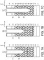
- FIGS. 1A to 2C are cross-sectional views showing a method of manufacturing a semiconductor device of a first embodiment
- FIG. 3 is a cross-sectional view showing a structure of a semiconductor device of the first embodiment.
- a method of manufacturing a semiconductor device includes forming a first film on a substrate. The method further includes performing a first process of forming a concave portion in the first film and forming a second film on a surface of the first film that is exposed in the concave portion by using a first gas containing a carbon element and a fluorine element. The method further includes performing a second process of exposing the second film to a second gas containing a hydrogen element or a fluid generated from the second gas.
- FIGS. 1A to 2C are cross-sectional views showing a method of manufacturing a semiconductor device of a first embodiment.
- the semiconductor device of the present embodiment is a three-dimensional semiconductor memory.
- a lower layer 2 is formed on a substrate 1 .
- a stacked film alternately including a plurality of first insulating layers 3 and a plurality of second insulating layers 4 is formed on the lower layer 2 .
- This stacked film is an example of a first film.
- an upper layer 5 is formed on the stacked film.
- a hard mask layer 6 is formed on the upper layer 5 .
- FIG. 1A shows an X-direction and a Y-direction which are parallel to the surface of the substrate 1 and perpendicular to each other, and a Z-direction perpendicular to the surface of the substrate 1 .
- the +Z-direction is regarded as the upward direction
- the ⁇ Z-direction is regarded as the downward direction.
- the ⁇ Z-direction may coincide with the direction of gravity or may not coincide with the direction of gravity.
- An example of the lower layer 2 is an insulator such as a silicon oxide film (SiO 2 ) or a silicon nitride film (SiN), or a conducting layer formed between insulators.
- An example of the first insulating layer 3 is a silicon nitride film.
- An example of the second insulating layer 4 is a silicon oxide film.
- An example of the upper layer 5 is an insulator such as a silicon oxide film or a silicon nitride film, or a conducting layer formed between insulators.
- An example of the hard mask layer 6 is an organic hard mask layer.
- an opening pattern for forming a memory hole M is formed in the hard mask layer 6 by lithography and etching.
- a first process of etching the first insulating layers 3 , the second insulating layers 4 and the upper layer 5 is performed.
- the memory hole M is formed in the first insulating layers 3 , the second insulating layer 4 and the upper layer 5 in the middle thereof.
- the memory hole M is an example of a concave portion.
- the first process is performed using a first gas G 1 containing a carbon element and a fluorine element.
- the first gas G 1 of the present embodiment contains C x H y F z gas.
- C denotes a carbon element
- H denotes a hydrogen element
- F denotes a fluorine element
- x is an integer of one or more
- y is an integer of zero or more
- z is an integer of one or more (x ⁇ 1, y ⁇ 0 and z ⁇ 1).
- C x H y F z is a fluorocarbon
- C x H y F z is a hydrofluorocarbon.
- the C x H y F z gas include C 4 F 6 gas, C 4 F 8 gas, CH 2 F 2 gas and the like.
- etching with C x H y F z plasma is performed, and a sidewall film 11 is formed on the surfaces and the like of the first insulating layers 3 , the second insulating layers 4 and the upper layer 5 that are exposed in the memory hole M ( FIG. 1A ).
- the sidewall film 11 of the present embodiment is a fluorocarbon film containing a carbon element and a fluorine element.
- the sidewall film 11 is an example of a second film.
- FIG. 1B shows a reformed sidewall film 12 obtained by reforming the sidewall film 11 .
- the second process is performed using a second gas G 2 containing a hydrogen element.
- the second gas G 2 of the present embodiment contains H 2 S (hydrogen sulfide) gas.
- S denotes a sulfur element.
- the sidewall film 11 is reformed by the sidewall film 11 exposed to the H 2 S gas or a fluid generated from the H 2 S gas (for example, exposed to H 2 S plasma).
- the sidewall film 11 of the present embodiment is a fluorocarbon film containing a carbon element and a fluorine element.
- the sidewall film 11 functions as a protection film in etching, for example, when high energy ions are incident on the sidewall film 11 , there can be a case where the sidewall film 11 contributes the etching. In other words, it is concerned that the sidewall film 11 promotes etching of the inside of the memory hole M. The reason is that the sidewall film 11 contributes to be a supply source of CF a in the following chemical equation (1). SiO 2 +CF a ⁇ SiF b ⁇ +CO c ⁇ (1) where a, b and c represent composition ratios.
- the sidewall film 11 is reformed. Specifically, fluorine in the sidewall film 11 is caused to react with hydrogen in the second gas to be eliminated as hydrogen fluoride. Thereby, the carbon-richer reformed sidewall film 12 than the sidewall film 11 can be obtained, which can reduce a fluorine concentration in the reformed sidewall film 12 than a fluorine concentration in the sidewall film 11 . Accordingly, for example, even when high energy ions are incident on the reformed sidewall film 12 , the reaction in chemical equation (1) hardly occurs, which suppresses etching of the inside of the memory hole M.
- the sidewall film 11 can be suppressed from contributing etching, and the reformed sidewall film 12 can be caused to function as a protection film. Thereby, the shape of the memory hole M can be suppressed from bowing.
- the second gas G 2 may contain only H 2 S gas, or may contain H 2 S gas and other gas. In the latter case, it is desirable that the flow rate (or pressure) of the H 2 S gas be set to occupy 80% or more of the flow rate (or pressure) of the second gas G 2 . Thereby, the sidewall film 11 can be sufficiently reformed with the second gas G 2 .
- the second gas G 2 may contain He (helium) gas, which has a low atomic weight, a low sputtering rate, and poor chemical reactivity. In this case, it is desirable that the sum total of the flow rate (or pressure) of the H 2 S gas and the flow rate (or pressure) of the He gas be set to occupy 80% or more of the flow rate (or pressure) of the second gas G 2 .
- the second gas G 2 in this case may contain only H 2 S gas and He gas, or further contain other gas.
- the first process and the second process are alternately performed after that, and thereby, the memory hole M is completed.
- the memory hole M of the present embodiment is formed by alternately feeding the first gas G 1 and the second gas G 2 .
- a plurality of first processes and a plurality of second processes are alternately performed in the same reaction chamber.
- the first process of etching the first insulating layers 3 and the second insulating layers 4 using the first gas G 1 is performed again ( FIG. 1C ).
- the process of forming the memory hole M progresses to lower the bottom face of the memory hole M.
- etching with C x H y F z plasma is performed, and a sidewall film 13 is formed on the surfaces of the first insulating layers 3 and the second insulating layers 4 that are exposed in the memory hole M.
- the sidewall film 13 has a similar property to that of the aforementioned sidewall film 11 , and is formed below the reformed sidewall film 12 .
- the sidewall film 13 is also an example of the second film.
- FIG. 2A shows a reformed sidewall film 14 obtained by reforming the sidewall film 13 .
- the sidewall film 13 is reformed by the sidewall film 13 exposed to H 2 S plasma.
- the reformed sidewall film 14 has a similar property to that of the aforementioned reformed sidewall film 12 .
- the first process of etching the first insulating layers 3 and the second insulating layers 4 using the first gas G 1 is performed again ( FIG. 2B ).
- the process of forming the memory hole M progresses to lower the bottom face of the memory hole M.
- etching with C x H y F z plasma is performed, and a sidewall film 15 is formed on the surfaces of the first insulating layers 3 and the second insulating layers 4 that are exposed in the memory hole M.
- the sidewall film 15 has a similar property to that of the aforementioned sidewall films 11 and 13 , and is formed below the reformed sidewall film 14 .
- the bottom face of the memory hole M reaches the substrate 1 , and the memory hole M is completed.
- the second process is performed again after that.
- a memory insulator 7 and a channel semiconductor layer 8 are sequentially formed in the memory hole M ( FIG. 2C ).
- the memory insulator 7 is formed by sequentially forming a first insulator (block insulator), a charge storage layer and a second insulator (tunnel insulator) in the memory hole M.
- the semiconductor device of the present embodiment is manufactured.
- the second gas G 2 may contain SF 6 (sulfur hexafluoride) gas. Thereby, the shape of the memory hole M can be more effectively suppressed from bowing. It is desirable that the flow rate (or pressure) of the SF 6 gas be set to occupy less than 20% of the flow rate (or pressure) of the second gas G 2 .
- the second gas G 2 in this case may contain only H 2 S gas and SF 6 gas, or may further contain other gas (for example, He gas).
- H 2 S gas and SF 6 gas The action of H 2 S gas and SF 6 gas is understood as follows.
- H 2 S/SF 6 plasma When H 2 S/SF 6 plasma is caused to impact on a fluorocarbon film which is the sidewall films 11 and 13 , F in the fluorocarbon film is abstracted by H. Thereby, the C-content in the fluorocarbon film increases, and C—C bonds in the fluorocarbon film increase.
- S in the H 2 S/SF 6 plasma is incorporated into the fluorocarbon film also to form C—S—C bonds. Since C—C bonds and C—S bonds are more stable in energy than C—F bonds and C—H bonds, the fluorocarbon film becomes stronger.
- etching resistance increases, which can suppress the diameter of the memory hole from widening during the processing of the memory hole M.
- the aforementioned first and second processes can also be applied to processing of films other than a stacked film of the first and second insulating layers 3 and 4 .
- the aforementioned first and second processes can also be applied to a case of forming a contact hole in an interlayer dielectric, and a case of forming a memory hole in a stacked film including a plurality of electrode layers (for example, polysilicon layers) and a plurality of insulating layers (for example, silicon oxide films).
- the aforementioned first and second processes can also be applied to a case of forming a shallow trench in the substrate 1 or in a layer on the substrate 1 .
- the hard mask layer 6 may be a carbon-containing film such as a carbon layer or a metal-containing layer such as a tungsten layer.
- Plasma conditions for the H 2 S/SF 6 plasma can be arbitrarily set.
- each first process is performed for 5 or more seconds, and each second process is also performed for 5 or more seconds.
- the performing time of the second process is sufficient to be secured to some extent, and hence, each second process of the present embodiment is performed for 5 or more seconds and less than 100 seconds. In the present embodiment, approximately 2 times to 20 times of first processes and approximately 2 times to 20 times of second processes are performed.
- the first insulating layers 3 (silicon nitride films) are replaced by electrode layers in a replacing step performed after the steps in FIGS. 1A to 2C .
- the replacing step hollows are formed between the second insulating layers 4 and the like by removing the first insulating layers 3 , and the electrode layers are embedded in the hollows.
- An example of the electrode layers is described with FIG. 3 .
- FIG. 3 is a cross-sectional view showing a structure of the semiconductor device of the first embodiment.
- FIG. 3 exemplarily shows a semiconductor device manufactured by the method of the present embodiment.
- FIG. 3 shows a memory cell part and a step contact part of a three-dimensional semiconductor memory.
- the lower layer 2 is configured of a lower insulator 2 a , a source-side conducting layer 2 b and an upper insulator 2 c
- the upper layer 5 is configured of a protecting insulator 5 a , a drain-side conducting layer 5 b , a first interlayer dielectric 5 c and a second interlayer dielectric 5 d .
- the first insulating layers 3 are replaced by electrode layers 3 ′ including tungsten layers and the like.
- the stacked film alternately including the plurality of electrode layers 3 ′ and the plurality of second insulating layers 4 is an example of a third film.
- FIG. 3 further shows a first insulator 7 a , a charge storage layer 7 b and a second insulator 7 c which constitute the memory insulator 7 .
- the memory insulator 7 and the channel semiconductor layer 8 are formed, for example, by sequentially forming the first insulator 7 a , the charge storage layer 7 b and the second insulator 7 c on the surface of the memory hole M, removing the first insulator 7 a , the charge storage layer 7 b and the second insulator 7 c from the bottom part of the memory hole M, and after that, embedding the channel semiconductor layer 8 in the memory hole M.
- the channel semiconductor layer 8 is electrically connected to a diffusion layer L in the substrate 1 .
- the memory insulator 7 and the channel semiconductor layer 8 are an example of a fourth film.
- An insulator called a core material may be further embedded in the memory hole M.
- the memory hole M of the present embodiment has a shape, for example, shown in FIG. 2C .
- FIG. 3 further shows contact plugs 9 formed in contact holes H of the upper layer 5 .
- Each contact plug 9 is formed so as to be electrically connected to the corresponding electrode layer 3 ′.
- the memory hole M of the present embodiment is formed by alternately performing a plurality of first processes using the first gas G 1 containing the carbon element and the fluorine element and a plurality of second processes using the second gas G 2 containing the hydrogen element. Therefore, according to the present embodiment, the shape of the memory hole M can be suppressed from bowing, which can appropriately realize the memory hole M with a high aspect ratio.
- the first gas G 1 and the second gas G 2 may be other than the aforementioned gases.
- the H 2 S gas in the second gas G 2 may be replaced by NH 3 (ammonia) gas, H 2 O (water) gas, H 2 (hydrogen) gas or the like.
- Any of H 2 S gas, NH 3 gas, H 2 O gas and H 2 gas contains one or more elements of S, N, O and H, and any of S 2 gas, N 2 gas, O 2 gas and H 2 gas has a vapor pressure of 10 Pa or more at 150° C.
- H 2 S gas when using H 2 S gas, NH 3 gas, H 2 O gas or H 2 gas, simple substance gases such as S 2 gas, N 2 gas, O 2 gas and H 2 gas which are generated through elimination of H with plasma hardly block up the memory hole M. Therefore, H 2 S gas, NH 3 gas, H 2 O gas and H 2 gas are suitable for their use in the reaction chamber.
- the H 2 S gas in the second gas G 2 may be replaced by gas which is gas of a compound containing a hydrogen element and any element ⁇ and in which the vapor pressure of simple substance gas of the element ⁇ is 10 Pa or more at 150° C. Examples of such gas are PH 3 gas and HI gas, and the vapor pressures of P 2 gas and I 2 gas is 10 Pa or more at 150° C.
- S, N, O and the element ⁇ are examples of a first element.
- the He gas in the second gas G 2 may be replaced by Ar (argon) gas, Kr (krypton) gas or Xe (xenon) gas.
- the SF 6 gas in the second gas G 2 may be replaced by COS (carbonyl sulfide) gas. SF 6 gas and COS gas are examples of gas containing a sulfur element.
Landscapes
- Semiconductor Memories (AREA)
- Physics & Mathematics (AREA)
- Engineering & Computer Science (AREA)
- Plasma & Fusion (AREA)
- Non-Volatile Memory (AREA)
- Drying Of Semiconductors (AREA)
- Internal Circuitry In Semiconductor Integrated Circuit Devices (AREA)
Abstract
Description
SiO2+CFa→SiFb↑+COc↑ (1)
where a, b and c represent composition ratios.
Claims (27)
Priority Applications (1)
| Application Number | Priority Date | Filing Date | Title |
|---|---|---|---|
| US17/879,108 US12334338B2 (en) | 2017-12-20 | 2022-08-02 | Method of manufacturing semiconductor device |
Applications Claiming Priority (3)
| Application Number | Priority Date | Filing Date | Title |
|---|---|---|---|
| JPJP2017-244253 | 2017-12-20 | ||
| JP2017-244253 | 2017-12-20 | ||
| JP2017244253A JP7137927B2 (en) | 2017-12-20 | 2017-12-20 | Semiconductor device manufacturing method |
Related Child Applications (1)
| Application Number | Title | Priority Date | Filing Date |
|---|---|---|---|
| US17/879,108 Continuation US12334338B2 (en) | 2017-12-20 | 2022-08-02 | Method of manufacturing semiconductor device |
Publications (2)
| Publication Number | Publication Date |
|---|---|
| US20190189423A1 US20190189423A1 (en) | 2019-06-20 |
| US11437232B2 true US11437232B2 (en) | 2022-09-06 |
Family
ID=66814663
Family Applications (2)
| Application Number | Title | Priority Date | Filing Date |
|---|---|---|---|
| US16/059,222 Active US11437232B2 (en) | 2017-12-20 | 2018-08-09 | Method of manufacturing semiconductor device |
| US17/879,108 Active 2039-04-07 US12334338B2 (en) | 2017-12-20 | 2022-08-02 | Method of manufacturing semiconductor device |
Family Applications After (1)
| Application Number | Title | Priority Date | Filing Date |
|---|---|---|---|
| US17/879,108 Active 2039-04-07 US12334338B2 (en) | 2017-12-20 | 2022-08-02 | Method of manufacturing semiconductor device |
Country Status (2)
| Country | Link |
|---|---|
| US (2) | US11437232B2 (en) |
| JP (1) | JP7137927B2 (en) |
Cited By (1)
| Publication number | Priority date | Publication date | Assignee | Title |
|---|---|---|---|---|
| US20220384180A1 (en) * | 2017-12-20 | 2022-12-01 | Kioxia Corporation | Method of manufacturing semiconductor device |
Families Citing this family (9)
| Publication number | Priority date | Publication date | Assignee | Title |
|---|---|---|---|---|
| JP2021106212A (en) * | 2019-12-26 | 2021-07-26 | 東京エレクトロン株式会社 | Etching method, substrate processing apparatus, and substrate processing system |
| CN115023464B (en) | 2020-01-24 | 2024-06-11 | Nok株式会社 | Acrylic rubber composition |
| JP2021150380A (en) | 2020-03-17 | 2021-09-27 | キオクシア株式会社 | Film treatment method and manufacturing method of semiconductor device |
| JP7463238B2 (en) | 2020-09-08 | 2024-04-08 | キオクシア株式会社 | Semiconductor manufacturing apparatus and method for manufacturing semiconductor device |
| JP2022046329A (en) * | 2020-09-10 | 2022-03-23 | キオクシア株式会社 | Semiconductor device and method for manufacturing the same |
| JP2022115656A (en) | 2021-01-28 | 2022-08-09 | キオクシア株式会社 | Manufacturing method of semiconductor device |
| TW202247287A (en) * | 2021-04-01 | 2022-12-01 | 日商東京威力科創股份有限公司 | Substrate processing method and substrate processing device |
| US20240420927A1 (en) * | 2021-11-03 | 2024-12-19 | Lam Research Corporation | System and method for carbon plug formation |
| CN121890304A (en) * | 2023-09-28 | 2026-04-17 | 东京毅力科创株式会社 | Etching method and plasma treatment device |
Citations (19)
| Publication number | Priority date | Publication date | Assignee | Title |
|---|---|---|---|---|
| JPH06275581A (en) | 1993-03-24 | 1994-09-30 | Sony Corp | Manufacture of semiconductor device |
| WO2004003988A1 (en) | 2002-06-27 | 2004-01-08 | Tokyo Electron Limited | Plasma processing method |
| US20060003577A1 (en) | 2004-07-01 | 2006-01-05 | Semiconductor Leading Edge Technologies, Inc. | Method of manufacturing a semiconductor device |
| US20060261516A1 (en) * | 2003-03-26 | 2006-11-23 | Riken | Process for producing dielectric insulating thin film, and dielectric insulating material |
| JP2014017406A (en) | 2012-07-10 | 2014-01-30 | Tokyo Electron Ltd | Plasma processing method and plasma processing apparatus |
| US20140030638A1 (en) * | 2012-07-30 | 2014-01-30 | Chang Ju Choi | Photomask processing techniques |
| US20140206198A1 (en) * | 2011-09-29 | 2014-07-24 | Kabushiki Kaisha Toshiba | Deposit removal method |
| US20140273487A1 (en) * | 2013-03-13 | 2014-09-18 | Applied Materials, Inc. | Pulsed dc plasma etching process and apparatus |
| JP2014187191A (en) | 2013-03-22 | 2014-10-02 | Toshiba Corp | Semiconductor storage device manufacturing method and semiconductor storage device |
| US20160071957A1 (en) | 2014-09-05 | 2016-03-10 | Kabushiki Kaisha Toshiba | Method for manufacturing semiconductor device |
| US20160079264A1 (en) | 2014-09-12 | 2016-03-17 | Kabushiki Kaisha Toshiba | Nonvolatile semiconductor memory device and method for manufacturing same |
| JP2016051750A (en) | 2014-08-29 | 2016-04-11 | 東京エレクトロン株式会社 | Etching method |
| US20160126252A1 (en) * | 2014-10-30 | 2016-05-05 | Kabushiki Kaisha Toshiba | Method for manufacturing semiconductor memory device and semiconductor memory device |
| US20160293609A1 (en) | 2015-04-01 | 2016-10-06 | Applied Materials, Inc. | Plasma enhanced chemical vapor deposition of films for improved vertical etch performance in 3d nand memory devices |
| US20160365249A1 (en) * | 2015-06-12 | 2016-12-15 | Kabushiki Kaisha Toshiba | Method for manufacturing semiconductor device |
| JP2016219771A (en) | 2015-05-14 | 2016-12-22 | 東京エレクトロン株式会社 | Etching method |
| US9613824B2 (en) | 2015-05-14 | 2017-04-04 | Tokyo Electron Limited | Etching method |
| US9754793B2 (en) | 2015-06-12 | 2017-09-05 | Toshiba Memory Corporation | Method for manufacturing semiconductor device |
| US20190043732A1 (en) * | 2017-08-02 | 2019-02-07 | Lam Research Corporation | High aspect ratio selective lateral etch using cyclic passivation and etching |
Family Cites Families (6)
| Publication number | Priority date | Publication date | Assignee | Title |
|---|---|---|---|---|
| US7473377B2 (en) * | 2002-06-27 | 2009-01-06 | Tokyo Electron Limited | Plasma processing method |
| JP2005116690A (en) * | 2003-10-06 | 2005-04-28 | Toshiba Corp | Manufacturing method of semiconductor device |
| JP2006275581A (en) | 2005-03-28 | 2006-10-12 | Citizen Watch Co Ltd | Indication plate for clock |
| US7309646B1 (en) * | 2006-10-10 | 2007-12-18 | Lam Research Corporation | De-fluoridation process |
| JP6211947B2 (en) * | 2013-07-31 | 2017-10-11 | 東京エレクトロン株式会社 | Manufacturing method of semiconductor device |
| JP7137927B2 (en) * | 2017-12-20 | 2022-09-15 | キオクシア株式会社 | Semiconductor device manufacturing method |
-
2017
- 2017-12-20 JP JP2017244253A patent/JP7137927B2/en active Active
-
2018
- 2018-08-09 US US16/059,222 patent/US11437232B2/en active Active
-
2022
- 2022-08-02 US US17/879,108 patent/US12334338B2/en active Active
Patent Citations (28)
| Publication number | Priority date | Publication date | Assignee | Title |
|---|---|---|---|---|
| JPH06275581A (en) | 1993-03-24 | 1994-09-30 | Sony Corp | Manufacture of semiconductor device |
| WO2004003988A1 (en) | 2002-06-27 | 2004-01-08 | Tokyo Electron Limited | Plasma processing method |
| US20060261516A1 (en) * | 2003-03-26 | 2006-11-23 | Riken | Process for producing dielectric insulating thin film, and dielectric insulating material |
| US20060003577A1 (en) | 2004-07-01 | 2006-01-05 | Semiconductor Leading Edge Technologies, Inc. | Method of manufacturing a semiconductor device |
| JP2006019480A (en) | 2004-07-01 | 2006-01-19 | Nec Electronics Corp | Manufacturing method of semiconductor device |
| US20140206198A1 (en) * | 2011-09-29 | 2014-07-24 | Kabushiki Kaisha Toshiba | Deposit removal method |
| US9412617B2 (en) * | 2012-07-10 | 2016-08-09 | Tokyo Electron Limited | Plasma processing method and plasma processing apparatus |
| JP2014017406A (en) | 2012-07-10 | 2014-01-30 | Tokyo Electron Ltd | Plasma processing method and plasma processing apparatus |
| US20140030638A1 (en) * | 2012-07-30 | 2014-01-30 | Chang Ju Choi | Photomask processing techniques |
| US20140273487A1 (en) * | 2013-03-13 | 2014-09-18 | Applied Materials, Inc. | Pulsed dc plasma etching process and apparatus |
| JP2014187191A (en) | 2013-03-22 | 2014-10-02 | Toshiba Corp | Semiconductor storage device manufacturing method and semiconductor storage device |
| US8946809B2 (en) | 2013-03-22 | 2015-02-03 | Kabushiki Kaisha Toshiba | Method for manufacturing semiconductor memory device and semiconductor memory device |
| JP2016051750A (en) | 2014-08-29 | 2016-04-11 | 東京エレクトロン株式会社 | Etching method |
| JP2016058456A (en) | 2014-09-05 | 2016-04-21 | 株式会社東芝 | Semiconductor device manufacturing method |
| US20160071957A1 (en) | 2014-09-05 | 2016-03-10 | Kabushiki Kaisha Toshiba | Method for manufacturing semiconductor device |
| US20160079264A1 (en) | 2014-09-12 | 2016-03-17 | Kabushiki Kaisha Toshiba | Nonvolatile semiconductor memory device and method for manufacturing same |
| JP2016062898A (en) | 2014-09-12 | 2016-04-25 | 株式会社東芝 | Nonvolatile semiconductor memory device and manufacturing method thereof |
| US20160126252A1 (en) * | 2014-10-30 | 2016-05-05 | Kabushiki Kaisha Toshiba | Method for manufacturing semiconductor memory device and semiconductor memory device |
| JP2016092044A (en) | 2014-10-30 | 2016-05-23 | 株式会社東芝 | Manufacturing method of semiconductor memory device |
| US20170162596A1 (en) | 2014-10-30 | 2017-06-08 | Kabushiki Kaisha Toshiba | Method for manufacturing semiconductor memory device and semiconductor memory device |
| JP2016197719A (en) | 2015-04-01 | 2016-11-24 | アプライド マテリアルズ インコーポレイテッドApplied Materials,Incorporated | Plasma enhanced chemical vapor deposition of film for improving vertical etching performance in 3d nand memory device |
| US20160293609A1 (en) | 2015-04-01 | 2016-10-06 | Applied Materials, Inc. | Plasma enhanced chemical vapor deposition of films for improved vertical etch performance in 3d nand memory devices |
| JP2016219771A (en) | 2015-05-14 | 2016-12-22 | 東京エレクトロン株式会社 | Etching method |
| US9613824B2 (en) | 2015-05-14 | 2017-04-04 | Tokyo Electron Limited | Etching method |
| US20160365249A1 (en) * | 2015-06-12 | 2016-12-15 | Kabushiki Kaisha Toshiba | Method for manufacturing semiconductor device |
| JP2017005178A (en) | 2015-06-12 | 2017-01-05 | 株式会社東芝 | Semiconductor device manufacturing method |
| US9754793B2 (en) | 2015-06-12 | 2017-09-05 | Toshiba Memory Corporation | Method for manufacturing semiconductor device |
| US20190043732A1 (en) * | 2017-08-02 | 2019-02-07 | Lam Research Corporation | High aspect ratio selective lateral etch using cyclic passivation and etching |
Cited By (2)
| Publication number | Priority date | Publication date | Assignee | Title |
|---|---|---|---|---|
| US20220384180A1 (en) * | 2017-12-20 | 2022-12-01 | Kioxia Corporation | Method of manufacturing semiconductor device |
| US12334338B2 (en) * | 2017-12-20 | 2025-06-17 | Kioxia Corporation | Method of manufacturing semiconductor device |
Also Published As
| Publication number | Publication date |
|---|---|
| JP2019110275A (en) | 2019-07-04 |
| JP7137927B2 (en) | 2022-09-15 |
| US20220384180A1 (en) | 2022-12-01 |
| US20190189423A1 (en) | 2019-06-20 |
| US12334338B2 (en) | 2025-06-17 |
Similar Documents
| Publication | Publication Date | Title |
|---|---|---|
| US12334338B2 (en) | Method of manufacturing semiconductor device | |
| US10153262B2 (en) | Semiconductor device and manufacturing method thereof | |
| US9397046B1 (en) | Fluorine-free word lines for three-dimensional memory devices | |
| US8227357B2 (en) | Methods of fabricating silicon oxide layers using inorganic silicon precursors and methods of fabricating semiconductor devices including the same | |
| US8314021B2 (en) | Method for fabricating semiconductor device with buried gates | |
| JP5441206B2 (en) | Semiconductor device and manufacturing method thereof | |
| US8319273B2 (en) | Self-aligned charge storage region formation for semiconductor device | |
| CN110120343B (en) | Manufacturing method of silicon nitride film and semiconductor device | |
| JP5706353B2 (en) | Semiconductor device and manufacturing method thereof | |
| US20130320426A1 (en) | Nonvolatile semiconductor memory device and method of fabricating the same | |
| US10872782B2 (en) | Method of manufacturing semiconductor device | |
| US8952445B2 (en) | Nonvolatile semiconductor memory device | |
| TWI788798B (en) | Manufacturing method of semiconductor device and semiconductor manufacturing device | |
| CN112103296B (en) | Method for manufacturing semiconductor structure | |
| KR100907931B1 (en) | Radical oxide film formation method and dual gate oxide film formation method using the same | |
| KR100554828B1 (en) | Device Separator Formation Method of Semiconductor Device | |
| US20060205149A1 (en) | Method of fabricating flash memory device | |
| US20250098163A1 (en) | Method for manufacturing three-dimensional memory device | |
| KR100794085B1 (en) | Manufacturing Method of Flash Memory Device | |
| CN114220817A (en) | Memory and manufacturing method thereof | |
| KR20090000352A (en) | Nonvolatile Memory Device and Manufacturing Method Thereof | |
| KR20090000328A (en) | Manufacturing method of nonvolatile memory device |
Legal Events
| Date | Code | Title | Description |
|---|---|---|---|
| AS | Assignment |
Owner name: TOSHIBA MEMORY CORPORATION, JAPAN Free format text: ASSIGNMENT OF ASSIGNORS INTEREST;ASSIGNORS:ISHINO, TAKAYA;TAKAHASHI, ATSUSHI;ZAIMA, KAZUNORI;SIGNING DATES FROM 20180726 TO 20180730;REEL/FRAME:046595/0465 |
|
| FEPP | Fee payment procedure |
Free format text: ENTITY STATUS SET TO UNDISCOUNTED (ORIGINAL EVENT CODE: BIG.); ENTITY STATUS OF PATENT OWNER: LARGE ENTITY |
|
| STPP | Information on status: patent application and granting procedure in general |
Free format text: DOCKETED NEW CASE - READY FOR EXAMINATION |
|
| STPP | Information on status: patent application and granting procedure in general |
Free format text: NON FINAL ACTION MAILED |
|
| STPP | Information on status: patent application and granting procedure in general |
Free format text: RESPONSE TO NON-FINAL OFFICE ACTION ENTERED AND FORWARDED TO EXAMINER |
|
| STPP | Information on status: patent application and granting procedure in general |
Free format text: DOCKETED NEW CASE - READY FOR EXAMINATION |
|
| STPP | Information on status: patent application and granting procedure in general |
Free format text: RESPONSE TO NON-FINAL OFFICE ACTION ENTERED AND FORWARDED TO EXAMINER |
|
| STPP | Information on status: patent application and granting procedure in general |
Free format text: FINAL REJECTION MAILED |
|
| STPP | Information on status: patent application and granting procedure in general |
Free format text: DOCKETED NEW CASE - READY FOR EXAMINATION |
|
| STPP | Information on status: patent application and granting procedure in general |
Free format text: NON FINAL ACTION MAILED |
|
| STPP | Information on status: patent application and granting procedure in general |
Free format text: RESPONSE TO NON-FINAL OFFICE ACTION ENTERED AND FORWARDED TO EXAMINER |
|
| AS | Assignment |
Owner name: KIOXIA CORPORATION, JAPAN Free format text: CHANGE OF NAME;ASSIGNOR:TOSHIBA MEMORY CORPORATION;REEL/FRAME:059059/0074 Effective date: 20191001 Owner name: TOSHIBA MEMORY CORPORATION, JAPAN Free format text: MERGER AND CHANGE OF NAME;ASSIGNORS:TOSHIBA MEMORY CORPORATION;K.K. PANGEA;REEL/FRAME:058981/0401 Effective date: 20180801 |
|
| STPP | Information on status: patent application and granting procedure in general |
Free format text: NOTICE OF ALLOWANCE MAILED -- APPLICATION RECEIVED IN OFFICE OF PUBLICATIONS |
|
| STPP | Information on status: patent application and granting procedure in general |
Free format text: AWAITING TC RESP., ISSUE FEE NOT PAID |
|
| STPP | Information on status: patent application and granting procedure in general |
Free format text: NOTICE OF ALLOWANCE MAILED -- APPLICATION RECEIVED IN OFFICE OF PUBLICATIONS |
|
| STPP | Information on status: patent application and granting procedure in general |
Free format text: PUBLICATIONS -- ISSUE FEE PAYMENT VERIFIED |
|
| STCF | Information on status: patent grant |
Free format text: PATENTED CASE |
|
| MAFP | Maintenance fee payment |
Free format text: PAYMENT OF MAINTENANCE FEE, 4TH YEAR, LARGE ENTITY (ORIGINAL EVENT CODE: M1551); ENTITY STATUS OF PATENT OWNER: LARGE ENTITY Year of fee payment: 4 |