US11430914B2 - Semiconductor light emitting device and method of manufacturing semiconductor light emitting device - Google Patents
Semiconductor light emitting device and method of manufacturing semiconductor light emitting device Download PDFInfo
- Publication number
- US11430914B2 US11430914B2 US16/727,539 US201916727539A US11430914B2 US 11430914 B2 US11430914 B2 US 11430914B2 US 201916727539 A US201916727539 A US 201916727539A US 11430914 B2 US11430914 B2 US 11430914B2
- Authority
- US
- United States
- Prior art keywords
- cone
- layer
- light extraction
- height
- shaped part
- Prior art date
- Legal status (The legal status is an assumption and is not a legal conclusion. Google has not performed a legal analysis and makes no representation as to the accuracy of the status listed.)
- Active, expires
Links
Images


Classifications
-
- H—ELECTRICITY
- H10—SEMICONDUCTOR DEVICES; ELECTRIC SOLID-STATE DEVICES NOT OTHERWISE PROVIDED FOR
- H10H—INORGANIC LIGHT-EMITTING SEMICONDUCTOR DEVICES HAVING POTENTIAL BARRIERS
- H10H20/00—Individual inorganic light-emitting semiconductor devices having potential barriers, e.g. light-emitting diodes [LED]
- H10H20/80—Constructional details
- H10H20/81—Bodies
- H10H20/819—Bodies characterised by their shape, e.g. curved or truncated substrates
- H10H20/82—Roughened surfaces, e.g. at the interface between epitaxial layers
-
- H01L33/22—
-
- H01L33/007—
-
- H01L33/12—
-
- H01L33/325—
-
- H—ELECTRICITY
- H10—SEMICONDUCTOR DEVICES; ELECTRIC SOLID-STATE DEVICES NOT OTHERWISE PROVIDED FOR
- H10H—INORGANIC LIGHT-EMITTING SEMICONDUCTOR DEVICES HAVING POTENTIAL BARRIERS
- H10H20/00—Individual inorganic light-emitting semiconductor devices having potential barriers, e.g. light-emitting diodes [LED]
- H10H20/01—Manufacture or treatment
- H10H20/011—Manufacture or treatment of bodies, e.g. forming semiconductor layers
- H10H20/013—Manufacture or treatment of bodies, e.g. forming semiconductor layers having light-emitting regions comprising only Group III-V materials
- H10H20/0133—Manufacture or treatment of bodies, e.g. forming semiconductor layers having light-emitting regions comprising only Group III-V materials with a substrate not being Group III-V materials
- H10H20/01335—Manufacture or treatment of bodies, e.g. forming semiconductor layers having light-emitting regions comprising only Group III-V materials with a substrate not being Group III-V materials the light-emitting regions comprising nitride materials
-
- H—ELECTRICITY
- H10—SEMICONDUCTOR DEVICES; ELECTRIC SOLID-STATE DEVICES NOT OTHERWISE PROVIDED FOR
- H10H—INORGANIC LIGHT-EMITTING SEMICONDUCTOR DEVICES HAVING POTENTIAL BARRIERS
- H10H20/00—Individual inorganic light-emitting semiconductor devices having potential barriers, e.g. light-emitting diodes [LED]
- H10H20/80—Constructional details
- H10H20/81—Bodies
- H10H20/815—Bodies having stress relaxation structures, e.g. buffer layers
-
- H—ELECTRICITY
- H10—SEMICONDUCTOR DEVICES; ELECTRIC SOLID-STATE DEVICES NOT OTHERWISE PROVIDED FOR
- H10H—INORGANIC LIGHT-EMITTING SEMICONDUCTOR DEVICES HAVING POTENTIAL BARRIERS
- H10H20/00—Individual inorganic light-emitting semiconductor devices having potential barriers, e.g. light-emitting diodes [LED]
- H10H20/80—Constructional details
- H10H20/81—Bodies
- H10H20/822—Materials of the light-emitting regions
- H10H20/824—Materials of the light-emitting regions comprising only Group III-V materials, e.g. GaP
- H10H20/825—Materials of the light-emitting regions comprising only Group III-V materials, e.g. GaP containing nitrogen, e.g. GaN
- H10H20/8252—Materials of the light-emitting regions comprising only Group III-V materials, e.g. GaP containing nitrogen, e.g. GaN characterised by the dopants
-
- H—ELECTRICITY
- H10—SEMICONDUCTOR DEVICES; ELECTRIC SOLID-STATE DEVICES NOT OTHERWISE PROVIDED FOR
- H10P—GENERIC PROCESSES OR APPARATUS FOR THE MANUFACTURE OR TREATMENT OF DEVICES COVERED BY CLASS H10
- H10P50/00—Etching of wafers, substrates or parts of devices
- H10P50/20—Dry etching; Plasma etching; Reactive-ion etching
- H10P50/24—Dry etching; Plasma etching; Reactive-ion etching of semiconductor materials
- H10P50/242—Dry etching; Plasma etching; Reactive-ion etching of semiconductor materials of Group IV materials
-
- H01L33/06—
-
- H01L33/145—
-
- H—ELECTRICITY
- H10—SEMICONDUCTOR DEVICES; ELECTRIC SOLID-STATE DEVICES NOT OTHERWISE PROVIDED FOR
- H10H—INORGANIC LIGHT-EMITTING SEMICONDUCTOR DEVICES HAVING POTENTIAL BARRIERS
- H10H20/00—Individual inorganic light-emitting semiconductor devices having potential barriers, e.g. light-emitting diodes [LED]
- H10H20/80—Constructional details
- H10H20/81—Bodies
- H10H20/811—Bodies having quantum effect structures or superlattices, e.g. tunnel junctions
- H10H20/812—Bodies having quantum effect structures or superlattices, e.g. tunnel junctions within the light-emitting regions, e.g. having quantum confinement structures
-
- H—ELECTRICITY
- H10—SEMICONDUCTOR DEVICES; ELECTRIC SOLID-STATE DEVICES NOT OTHERWISE PROVIDED FOR
- H10H—INORGANIC LIGHT-EMITTING SEMICONDUCTOR DEVICES HAVING POTENTIAL BARRIERS
- H10H20/00—Individual inorganic light-emitting semiconductor devices having potential barriers, e.g. light-emitting diodes [LED]
- H10H20/80—Constructional details
- H10H20/81—Bodies
- H10H20/816—Bodies having carrier transport control structures, e.g. highly-doped semiconductor layers or current-blocking structures
- H10H20/8162—Current-blocking structures
-
- H—ELECTRICITY
- H10—SEMICONDUCTOR DEVICES; ELECTRIC SOLID-STATE DEVICES NOT OTHERWISE PROVIDED FOR
- H10H—INORGANIC LIGHT-EMITTING SEMICONDUCTOR DEVICES HAVING POTENTIAL BARRIERS
- H10H20/00—Individual inorganic light-emitting semiconductor devices having potential barriers, e.g. light-emitting diodes [LED]
- H10H20/80—Constructional details
- H10H20/81—Bodies
- H10H20/822—Materials of the light-emitting regions
- H10H20/824—Materials of the light-emitting regions comprising only Group III-V materials, e.g. GaP
- H10H20/825—Materials of the light-emitting regions comprising only Group III-V materials, e.g. GaP containing nitrogen, e.g. GaN
-
- H—ELECTRICITY
- H10—SEMICONDUCTOR DEVICES; ELECTRIC SOLID-STATE DEVICES NOT OTHERWISE PROVIDED FOR
- H10H—INORGANIC LIGHT-EMITTING SEMICONDUCTOR DEVICES HAVING POTENTIAL BARRIERS
- H10H20/00—Individual inorganic light-emitting semiconductor devices having potential barriers, e.g. light-emitting diodes [LED]
- H10H20/80—Constructional details
- H10H20/872—Periodic patterns for optical field-shaping, e.g. photonic bandgap structures
Definitions
- the present invention relates to semiconductor light emitting devices.
- semiconductor light emitting devices such as light emitting diodes and laser diodes that emit blue light have been in practical use.
- Development of light emitting devices that output deep ultraviolet light having a shorter wavelength has also been pursued.
- a light emitting device for emitting deep ultraviolet light includes an aluminum gallium nitride (AlGaN) based n-type clad layer, active layer, p-type clad layer, etc. stacked successively on a substrate. Deep ultraviolet light emitted by the active layer is output from a light extraction surface of the substrate.
- AlGaN aluminum gallium nitride
- the external quantum efficiency of deep ultraviolet light output via the light extraction surface of the substrate of a deep ultraviolet light emitting device is as low as several % and that the shorter the wavelength of emitted light, the lower the external quantum efficiency.
- one illustrative purpose of the present invention is to provide a technology of increasing the light extraction efficiency of semiconductor light emitting devices.
- a semiconductor light emitting device is a semiconductor light emitting device including a light extraction layer having a light extraction surface, multiple cone-shaped parts formed in an array being provided on the light extraction surface.
- a proportion of an area occupied by the multiple cone-shaped parts per a unit area of the light extraction surface is not less than 65% and not more than 95% in a plan view of the light extraction surface, and an aspect ratio h/p defined as a proportion of a height h of the cone-shaped part relative to a distance p between apexes of adjacent cone-shaped parts is not less than 0.3 and not more than 1.0.
- the concave-convex structure provided by forming multiple cone-shaped parts in an array on the light extraction surface inhibits total reflection of light occurring inside the light extraction surface and increases the efficiency of light output from the light extraction surface.
- the light extraction efficiency is suitably improved by controlling the aspect ratio of the cone-shaped part to be in a range 0.3-1.0 and configuring the proportion of the area occupied by the cone-shaped parts to be not less than 65% and not more than 95%. Accordingly, the embodiment makes it possible to improve the light extraction efficiency suitably by using a concave-convex structure of a shape that can be easily or possibly realized.
- a bottom the cone-shaped part may have a shape of a hexagon or a shape intermediate between a hexagon and a circle, and the proportion of the area occupied by the multiple cone-shaped parts per a unit area of the light extraction surface may be not less than 91% and not more than 95%.
- a neighborhood of the bottom of the cone-shaped part may have a hexagonal shape or a shape intermediate between a hexagon and a circle, and a neighborhood of the apex of the cone-shaped part may have a shape closer to a circle than the neighborhood of the bottom.
- the cone-shaped part may have a first portion having a first angle of inclination of a side surface and a second portion having a second angle of inclination of a side surface smaller than the first angle.
- the second portion is closer to the apex of the cone-shaped part than the first portion and has a larger height than the first portion.
- a height of the second portion may be not less than 1.1 times and not more than three times a height of the first portion.
- the first angle may be not less than 60° and not more than 85°, and the second angle may be not less than 40° and not more than 60°.
- the semiconductor light emitting device may include: a base structure including at least one of a sapphire (Al 2 O 3 ) layer and an aluminum nitride (AlN) layer; and a light emitting structure formed on the base structure and including an aluminum gallium nitride (AlGaN)-based or a gallium nitride (GaN)-based semiconductor layer that emits ultraviolet light of a wavelength of not less than 200 nm and not more than 400 nm.
- a base structure including at least one of a sapphire (Al 2 O 3 ) layer and an aluminum nitride (AlN) layer
- AlGaN aluminum gallium nitride
- GaN gallium nitride
- the light extraction layer may be the sapphire (Al 2 O 3 ) layer, the AlN layer or a silicon oxide (SiO x ) layer, or a silicon nitride layer (SiN x ) or an aluminum oxide layer (Al 2 O 3 ) of the base structure.
- Another embodiment of the present invention relates to a method of manufacturing a semiconductor light emitting device.
- the method is directed to manufacturing a semiconductor light emitting device including a light extraction layer having a light extraction surface, the method comprising: forming a mask having an array pattern on the light extraction layer; and etching the mask and the light extraction layer from above the mask.
- the etching includes first dry-etching for dry-etching the mask and the light extraction layer until the entirety of the mask is removed and second dry-etching for further dry-etching the light extraction layer after the mask is removed.
- Multiple cone-shaped parts are formed in an array on the light extraction surface in the first dry-etching such that an aspect ratio h/p defined as a proportion of a height h of the cone-shaped part relative to a distance p between apexes of adjacent cone-shaped parts is 1.1 or larger, and the multiple cone-shaped parts are further etched in the second dry-etching such that the aspect ratio h/p of the cone-shaped part is not less than 0.3 and not more than 1.0.
- the embodiment makes it possible configure the proportion of the area occupied by the multiple cone-shaped parts formed after the second dry-etching to be larger than the proportion of the area occupied by the multiple cone-shaped parts formed after the first dry-etching. This makes it easier to manufacture a light extraction surface having an improved light extraction efficiency by using a mask that can be easily or possibly manufactured.
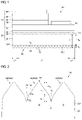
- FIG. 1 is a cross sectional view schematically showing a configuration of a semiconductor light emitting device according to the embodiment
- FIG. 2 is a cross-sectional view schematically showing a configuration of the concave-convex structure
- FIG. 3 is a top view schematically showing a configuration of the concave-convex structure
- FIG. 4 is a flowchart showing a method of manufacturing the semiconductor light emitting device
- FIG. 5 schematically shows a step of manufacturing the concave-convex structure
- FIG. 6 schematically shows a step of manufacturing the concave-convex structure
- FIG. 7 schematically shows a step of manufacturing the concave-convex structure
- FIG. 8 schematically shows a step of manufacturing the concave-convex structure
- FIG. 9 schematically shows a step of manufacturing the concave-convex structure
- FIGS. 10A-10E are electron microscope images of the concave-convex structure
- FIG. 11 is a graph showing a relationship between the proportion of the height of the second portion of the concave-convex structure according to the examples and the light output;
- FIG. 12 is a graph showing a relationship between the difference between the first angle and the second angle of the concave-convex structure according to the examples and the light output;
- FIG. 13 is a graph showing a relationship between the proportion of the area occupied by the concave-convex structure according to the examples and the light output.
- FIG. 1 is a cross sectional view schematically showing a configuration of a semiconductor light emitting device 10 according to the embodiment.
- the semiconductor light emitting device 10 includes a base structure 20 and a light emitting structure 30 .
- the base structure 20 includes a substrate 22 , a first base layer 24 , and a second base layer 26 .
- the light emitting structure 30 includes an n-type clad layer 32 , an active layer 34 , an electron blocking layer 36 , a p-type clad layer 38 , a p-side electrode 40 , and an n-side electrode 42 .
- the semiconductor light emitting device 10 is a semiconductor light emitting device configured to emit “deep ultraviolet light” having a central wavelength of about 365 nm or shorter.
- the active layer 34 is made of an aluminum gallium nitride (AlGaN)-based semiconductor material having a band gap of about 3.4 eV or larger.
- AlGaN aluminum gallium nitride
- AlGaN-based semiconductor material mainly refers to a semiconductor material containing aluminum nitride (AlN) and gallium nitride (GaN) and shall encompass a semiconductor material containing other materials such as indium nitride (InN). Therefore, “AlGaN-based semiconductor materials” as recited in this specification can be represented by a composition In 1-x-y Al x Ga y N (0 ⁇ x+y ⁇ 1, 0 ⁇ x ⁇ 1, 0 ⁇ y ⁇ 1).
- the AlGaN-based semiconductor material shall contain AlN, GaN, AlGaN, indium aluminum nitride (InAlN), indium gallium nitride (InGaN), or indium aluminum gallium nitride (InAlGaN).
- AlGaN-based semiconductor materials those materials that do not substantially contain AlN may be distinguished by referring to them as “GaN-based semiconductor materials”. “GaN-based semiconductor materials” mainly contain GaN or InGaN and encompass materials that additionally contain a slight amount of AlN. Similarly, of “AlGaN-based semiconductor materials”, those materials that do not substantially contain GaN may be distinguished by referring to them as “AlN-based semiconductor materials”. “AlN-based semiconductor materials” mainly contain AlN or InAlN and encompass materials that additionally contain a slight amount of GaN.
- the substrate 22 is a sapphire (Al 2 O 3 ) substrate.
- the substrate 22 may be an aluminum nitride (AlN) substrate in one variation.
- the substrate 22 includes a first principal surface 22 a and a second principal surface 22 b opposite to the first principal surface 22 a .
- the first principal surface 22 a is a principal surface that is a crystal growth surface.
- the first principal surface 22 a is the (0001) plane of the sapphire substrate.
- the second principal surface 22 b is a principal surface that is the light extraction surface and is formed with a micro-concave-convex structure (texture structure) 50 of a submicron scale. The detail of the concave-convex structure 50 will be described later.
- the substrate 22 has a thickness t of 1 ⁇ m or larger.
- the substrate 22 has a thickness of about 5 ⁇ m, 10 ⁇ m, 100 ⁇ m, 300 ⁇ m, or 500 ⁇ m.
- the thickness t of the substrate 22 is twice the height h A of the concave-convex structure 50 or larger.
- the thickness t is ten times the height h A of the concave-convex structure 50 or larger.
- the height h B from the first principal surface 22 a of the substrate 22 to a boundary surface 22 c bordering the concave-convex structure 50 is larger than the height h A of the concave-convex structure 50 and twice the height h A of the concave-convex structure h A or larger.
- the first base layer 24 and the second base layer 26 are stacked on the first principal surface 22 a of the substrate 22 .
- the first base layer 24 is a layer made of an AlN-based semiconductor material and is, for example, an AlN(HT-AlN) layer gown at a high temperature.
- the second base layer 26 is a layer made of an AlGaN-based semiconductor material and is, for example, an undoped AlGaN(u-AlGaN) layer.
- the substrate 22 , the first base layer 24 , and the second base layer 26 function as a foundation layer (template) to form the n-type clad layer 32 and the layers above. These layers also function as a light extraction layer for extracting the deep ultraviolet light emitted by the active layer 34 outside and transmit the deep ultraviolet light emitted by the active layer 34 . It is preferred that the first base layer 24 and the second base layer 26 be made of an AlGaN-based or AlN-based material having an AlN ratio higher than that of the active layer 34 so as to increase the transmittance for the deep ultraviolet light emitted by the active layer 34 . It is further preferred that the first base layer 24 and the second base layer 26 be made of a material having a lower refractive index than the active layer 34 .
- the first base layer 24 and the second base layer 26 be made of a material having a higher refractive index than the substrate 22 .
- the n-type clad layer 32 is an n-type semiconductor layer provided on the second base layer 26 .
- the n-type clad layer 32 is made of an n-type AlGaN-based semiconductor material.
- the n-type clad layer 32 is an AlGaN layer doped with silicon (Si) as an n-type impurity.
- the composition ratio of the n-type clad layer 32 is selected to transmit the deep ultraviolet light emitted by the active layer 34 .
- the n-type clad layer 32 is formed such that the molar fraction of AlN is 40% or higher, and, preferably, 50% or higher.
- the n-type clad layer 32 has a band gap larger than the wavelength of the deep ultraviolet light emitted by the active layer 34 .
- the n-type clad layer 32 is formed to have a band gap of 4.3 eV or larger.
- the n-type clad layer 32 has a thickness of about 100 nm ⁇ 300 nm.
- the n-type clad layer 32 has a thickness of about 200 nm.
- the active layer 34 is formed in a partial region on the n-type clad layer 32 .
- the active layer 34 is made of an AlGaN-based semiconductor material and has a double heterojunction structure by being sandwiched by the n-type clad layer 32 and the electron blocking layer 36 .
- the active layer 34 may form a monolayer or multilayer quantum well structure.
- the quantum well structure like this can be formed by building a stack of a barrier layer made of an undoped AlGaN-based semiconductor material and a well layer made of an undoped AlGaN-based semiconductor material.
- the active layer 34 is formed to have a band gap of 3.4 eV or larger.
- the AlN composition ratio of the active layer 34 is selected so as to output deep ultraviolet light having a wavelength of 310 nm or shorter.
- the electron blocking layer 36 is formed on the active layer 34 .
- the electron blocking layer 36 is a layer made of a p-type AlGaN-based semiconductor material and is exemplified by an undoped AlGaN layer.
- the electron blocking layer 36 is formed such that the molar fraction of AlN is 40% or higher, and, preferably, 50% or higher.
- the electron blocking layer 36 may be formed such that the molar fraction of AlN is 80% or higher or may be made of an AlN-based semiconductor material that does not substantially contain GaN.
- the electron blocking layer 36 may be made of an AlGaN-based semiconductor material or an AlN-based semiconductor material doped with magnesium (Mg) as a p-type impurity.
- the electron blocking layer 36 has a thickness of about 1 nm ⁇ 10 nm. For example, the electron blocking layer 36 has a thickness of about 2 nm ⁇ 5 nm.
- the p-type clad layer 38 is formed on the electron blocking layer 36 .
- the p-type clad layer 38 is a layer made of a p-type AlGaN-based semiconductor material and is exemplified by a Mg-doped AlGaN layer.
- the composition ratio of the p-type clad layer 38 is selected such that the molar fraction of AlN in the p-type clad layer 38 is lower than that of the electron blocking layer 36 .
- the p-type clad layer 38 has a thickness of about 300 nm ⁇ 700 nm.
- the p-type clad layer 38 has a thickness of about 400 nm ⁇ 600 nm.
- the p-side electrode 40 is provided on the p-type clad layer 38 .
- the p-side electrode 40 is made of a material capable of establishing ohmic contact with the p-type clad layer 38 .
- the p-side electrode 40 is formed by a nickel (Ni)/gold (Au) stack structure.
- the n-side electrode 42 is provided on the n-type clad layer 32 .
- the n-side electrode 42 is a Ti/Al-based electrode and is formed by, for example, a titanium (Ti)/Al/Ti/Au or Ti/Al/Ni/Au stack structure.
- the concave-convex structure 50 is formed on the second principal surface (also referred to as the light extraction surface) 22 b of the substrate 22 that is the light extraction layer.
- the concave-convex structure 50 inhibits reflection or total reflection on the second principal surface 22 b and increases the light extraction efficiency of deep ultraviolet light output from the second principal surface 22 b .
- the concave-convex structure 50 has multiple cone-shaped parts 52 formed in an array on the light extraction surface.
- the cone-shaped part 52 is made of the same material as the substrate 22 .
- the cone-shaped part 52 is made of sapphire (Al 2 O 3 ) or aluminum nitride (AlN).
- the cone-shaped part 52 has a first portion 53 having a relatively large angle of inclination of the side surface and a second portion 54 having a relatively small angle of inclination of the side surface.
- the first portion 53 is located toward the bottom of the cone-shaped part 52 (toward the top of the plane of paper of FIG. 1 ), and the second portion 54 is located toward the apex of the cone-shaped part 52 (toward the bottom of the plane of paper of FIG. 1 ).
- the concave-convex structure 50 is formed on substantially the entirety of the second principal surface 22 b .
- the concave-convex structure 50 may be formed only in a restricted area on the second principal surface 22 b .
- the concave-convex structure 50 may be formed only in an inner region C 1 of the second principal surface 22 b and may not be formed in an outer region C 2 .
- the size of the outer region C 2 is not limited to a particular size.
- the outer region C 2 extends in a range of about 1 ⁇ m ⁇ 50 ⁇ m.
- FIG. 2 is a cross-sectional view schematically showing a configuration of the concave-convex structure 50 and represents a partial enlarged view of FIG. 1 .
- FIG. 2 is oriented upside down relative to FIG. 1 .
- the multiple cone-shaped parts 52 ( 52 a , 52 b , 52 c ) are arranged at a predetermined pitch p.
- the pitch p of the cone-shaped parts 52 is defined as a distance between apexes 56 of adjacent cone-shaped parts 52 (e.g., 52 b and 52 c ).
- the cone-shaped parts 52 is formed such that the pitch p between adjacent cone-shaped parts 52 is not less than 100 nm and not more than 1000 nm, and, for example, not less than 250 nm and not more than 600 nm.
- the multiple cone-shaped parts 52 are formed to have a substantially uniform height h A .
- the height h A of the cone-shaped part 52 is not less than 150 nm and not more than 900 nm and, preferably, not less than 240 nm and not more than 600 nm.
- the height h A of the cone-shaped part 52 is not less than 0.3 times and not more than 1.5 times and, preferably, not less than 0.5 times and not more than 1.0 times the pitch p of the cone-shaped part 52 .
- the height h of the cone-shaped part 52 is not less than 120 nm and not more than 600 nm and, preferably, not less than 200 nm and not more than 400 nm.
- the height h A of the cone-shaped part 52 may have certain (e.g., 5% ⁇ 30%) variability.
- the cone-shaped part 52 has the first portion 53 having a first angle ⁇ 1 of inclination of the side surface and the second portion 54 having a second angle ⁇ 2 of inclination of the side surface.
- the first portion 53 is a portion including a bottom 55 of the cone-shaped part 52
- the second portion 54 is a portion including the apex 56 of the cone-shaped part 52 .
- the first angle ⁇ 1 of the first portion 53 is an angle formed by the side surface of the cone-shaped part 52 and the boundary surface 22 c that could be seen as the bottom surface of the cone-shaped part 52 and is an angle of inclination of the side surface at the bottom 55 of the cone-shaped part 52 .
- the second angle ⁇ 2 of the second portion 54 is an angle of inclination of the side surface near the boundary between the first portion 53 and the second portion 54 .
- the first angle ⁇ 1 is larger than the second angle ⁇ 2 (i.e., ⁇ 1 > ⁇ 2 ). Therefore, the cone-shaped part 52 is shaped such that the inclination of the side surface is gentler near the apex 56 than near the bottom 55 .
- the first angle ⁇ 1 is 45° or larger and, preferably, not less than 60° and not more than 85°.
- the second angle ⁇ 2 is 60° or smaller and, preferably, not less than 40° and not more than 60°.
- An angle difference ⁇ ( ⁇ 1 - ⁇ 2 ) between the first angle ⁇ 1 and the second angle ⁇ 2 is preferably 10° or larger, and more preferably, 15° or larger or 20° or larger.
- the height h 2 of the second portion 54 is larger than the height h 1 of the first portion 53 .
- the height h 2 of the second portion 54 is preferably 1.1 times the height h 1 of the first portion 53 or larger and, more preferably, 1.5 times the height h 1 or larger.
- the height h 2 of the second portion 54 is about twice ⁇ three times the height h 1 of the first portion 53 . Therefore, the height h 2 of the second portion 54 preferably occupies 50% or larger of the total height h A of the cone-shaped part 52 and, more preferably, occupies 60% ⁇ 75% of the total height h A .
- the height h 2 of the second portion 54 is preferably 80% or smaller than the total height h A of the cone-shaped part, and the first portion 53 occupies a certain proportion (20% or larger).
- each of the first portion 53 and the second portion 54 of the cone-shaped part 52 illustrated has a constant angle of inclination, and the side surface is formed to be straight in a cross-sectional view of FIG. 2 perpendicular to the boundary surface 22 c .
- the angle of inclination of the side surface of the first portion 53 and the second portion 54 may not be constant, and the side surface may be shaped such that the angle of inclination varies gradually.
- the first portion 53 may be shaped such that the angle of inclination ⁇ 1 is substantially constant
- the second portion 54 may be shaped such that the angle of inclination ⁇ 2 grows gradually smaller toward the apex 56 .
- the side surface of the second portion 54 may be convexly curved outward from the cone-shaped part 52 .
- FIG. 3 is a top view schematically showing a configuration of the concave-convex structure 50 and schematically shows an arrangement of the multiple cone-shaped parts 52 of FIG. 2 .
- FIG. 2 corresponds to an A-A cross section of FIG. 3 .
- the multiple cone-shaped parts 52 are arranged in a triangular grid pattern as illustrated.
- the outer profile of the cone-shaped part 52 has a shape similar to a hexagon and has a shape intermediate between a hexagon and a circle.
- a shape intermediate between a hexagon and a circle refers to a shape in which the profile line is substantially located in a region between a hexagon and an inscribed circle thereof and refers to a shape produced by rounding the corners of a heptagon or a polygon having a larger number of corners (e.g., octagon, dodecagon, icositetragon) or of a hexagon or a polygon having a larger number or corners.
- the cone-shaped part may be shaped such that 10% or larger or, preferably, 20% or larger of the area between a hexagon and an inscribed circle thereof is located inside the profile line.
- the area occupied will be larger than the area of the reference circle (e.g., the inscribed circle).
- the proportion of the area occupied by the multiple cone-shaped parts 52 per a unit area in a plan view of the second principal surface 22 b is increased accordingly.
- the proportion of the area occupied would be approximately 90%.
- the cone-shaped part 52 may be shaped such that the plan view of the second principal surface 22 b , i.e., the cross section perpendicular to the direction of height of the cone-shaped part 52 varies in the direction of height.
- the cross-sectional shape of the first portion 53 perpendicular to the direction of height may be different from the cross-sectional shape of the second portion 54 perpendicular to the direction of height.
- the cross-sectional shape of the first portion 53 perpendicular to the direction of height may be a shape intermediate between a hexagon and a circle, and the cross-sectional shape of the second portion 54 perpendicular to the direction of height may have a shape closer to a circle than the first portion.
- the cross-sectional shape of the second portion 54 perpendicular to the direction of height may have corners more rounded and having smaller curvature (i.e., larger radius of curvature) than those of the cross sectional-shape of the first portion 53 perpendicular to the direction of height.
- the shape difference between the first portion 53 and the second portion 54 may be defined by the circularity.
- a determination as to whether a shape is relatively similar to a circle may be made by referring to a difference between the maximum radius of curvature and the minimum radius of curvature defined in the JIS standard (JISB0621-1984).
- the second portion 54 may be have a shape with a smaller circularity than the first portion 53 .
- the gap between adjacent cone-shaped parts 52 is small, and the width or diameter ⁇ of the cone-shaped part 52 is preferably nearly equal to the pitch p of the adjacent cone-shaped parts 52 .
- the diameter ⁇ of the cone-shaped part 52 is configured to be 0.85 times the pitch p or larger and, preferably, 0.9 times the pitch p or larger. By configuring the diameter ⁇ of the cone-shaped part 52 to be 0.85 times the pitch p or larger, the proportion of the multiple cone-shaped parts 52 occupying a unit area in a plan view of the second principal surface 22 b is ensured to be 65% or higher.
- FIG. 4 is a flowchart showing a method of manufacturing the semiconductor light emitting device 10 .
- a light emitting device provided with a light extraction layer is prepared (S 10 ), and a resin mask of an array pattern is formed on the light extraction layer (S 12 ).
- a first dry-etching step is performed to dry-etch the mask and the light extraction layer from the above mask and etch the mask and the layer until the entirety of the mask is removed (S 14 ).
- a second dry-etching step is performed to further dry-etch the light extraction surface after the mask is removed in the first dry-etching step (S 16 ).
- the first dry-etching step to remove the mask and the second dry-etching step to overetch the layer after the mask is removed are performed.
- the substrate 22 not formed with the concave-convex structure 50 is prepared, and the first base layer 24 , the second base layer 26 , the n-type clad layer 32 , the active layer 34 , the electron blocking layer 36 , and the p-type clad layer 38 are stacked successively on the first principal surface 22 a of the substrate 22 .
- the second base layer 26 , the n-type clad layer 32 , the active layer 34 , the electron blocking layer 36 , and the p-type clad layer 38 made of an AlGaN-based semiconductor material or a GaN-based semiconductor material can be formed by a well-known epitaxial growth method such as the metalorganic vapor phase epitaxy (MOVPE) method and the molecular beam epitaxy (MBE) method.
- MOVPE metalorganic vapor phase epitaxy
- MBE molecular beam epitaxy
- portions of the active layer 34 , the electron blocking layer 36 , and the p-type clad layer 38 stacked on the n-type clad layer 32 are removed to expose a partial region of the n-type clad layer 32 .
- portions of the active layer 34 , the electron blocking layer 36 , and the p-type clad layer 38 may be removed so as to expose the partial region of the n-type clad layer 32 .
- the n-side electrode 42 is then formed on the partial region of the n-type clad layer 32 exposed, and the p-side electrode 40 is formed on the p-type clad layer 38 .
- the metal layers forming the p-side electrode 40 and the n-side electrode 42 may be formed by a well-known method such as electron beam deposition and sputtering.
- FIGS. 5 ⁇ 9 schematically show steps of manufacturing the concave-convex structure 50 and shows a step of processing a processed surface 60 c of the light extraction layer 60 in which the concave-convex structure 50 has yet been formed.
- the light extraction layer 60 is a layer in which the light extraction surface should be formed and is a layer corresponding to the substrate 22 of the semiconductor light emitting device 10 shown in FIG. 1 .
- FIG. 5 shows a step of forming a mask 62 on the light extraction layer 60 .
- the processed surface 60 c of the light extraction layer 60 is the (0001) plane (c plane) of the sapphire substrate.
- the mask 62 includes an array pattern corresponding to the cone-shaped parts 52 of the concave-convex structure 50 and includes a multiple columns 64 arranged in an array.
- the multiple columns 64 arranged in a triangular grid pattern, and each column has a prism or cylinder shape.
- the column 64 may be provided with a slight taper angle and may be shaped in a truncated pyramid or a truncated cone.
- the mask 62 is formed by a resist resin by using the nanoimprinting technology.
- the method of forming the mask 62 is not limited to any particular method, and the mask 62 may be formed by using a lithographic technology based on exposure or electron-beam printing.
- the mask 62 is formed such that the pitch p c of adjacent columns 64 is identical to the pitch p of the cone-shaped parts 52 .
- the height h c of the column 64 is determined based on the height h 0 of a cone-shaped part 6 formed in the first dry-etching step (see FIG. 7 , the detail will be described later) and the ratio between the etching rates of the light extraction layer 60 and the mask 62 . Denoting the etching rate of the light extraction layer 60 by e and the etching of the mask 62 by e c , the height h of the column 64 can be determined by an expression h c ⁇ h 0 *e c /e.
- the height h c of the column 64 may be slightly larger than the value given by the above expression or larger than the value h 0 *e c /e by about 5% ⁇ 15%.
- the diameter ⁇ c of the column 64 is smaller than the pitch p c of the columns 64 and is, for example, about 80% ⁇ 95% of the pitch p c .
- the diameter ⁇ c of the column 64 may be smaller than the diameter ⁇ of the cone-shaped part 52 ultimately formed.
- a dry-etching process is then performed from above the mask 62 .
- Reactive ion etching may be used as a method of dry-etching the light extraction layer 60 and the mask 62 .
- plasma etching using inductive coupling plasma ICP
- the gas species used in plasma etching is not limited to any particular type, but it is preferred to use a chlorine-based gas such as chlorine (Cl 2 ) and boron trichloride (BCl 3 ) as an etching gas.
- an etching gas like the above, it is possible to suitably etch sapphire or aluminum nitride forming the light extraction layer 60 and etch the resist resin forming the mask 62 .
- FIG. 6 schematically shows the dry-etched light extraction layer 60 and the mask 62 and shows a state in the middle of the first dry-etching step described above.
- the column 64 is isotropically etched from above and from side. As the etching step proceeds, the height h c and the diameter ⁇ c of the column 64 grow smaller. Meanwhile, those portions of the light extraction layer 60 located below the mask 62 that are not covered with the mask 62 are etched. Since the covered area of the column 64 is reduced toward the center of the column 64 with time, the area of the light extraction layer 60 that is etched grows larger with time.
- the etching volume in the direction of depth of the light extraction layer 60 varies depending on the distance from the center of the column 64 with the result that the cone-shaped part 66 having an inclined surface 67 and similar to a truncated cone or a truncated pyramid is formed below the mask 62 .
- the cone-shaped part 66 is formed at a position corresponding to the array pattern of the mask 62 and is formed in a position corresponding to each of the multiple columns 64 .
- FIG. 7 schematically shows the dry-etched light extraction layer 60 and the mask 62 and shows a state that occurs immediately before the first dry-etching step is terminated.
- the dry-etching step is allowed to proceed from the state shown in FIG. 6 , the column 64 grows even smaller, and the entirety of the mask 62 is ultimately removed from above the light extraction layer 60 .
- the light extraction layer 60 is etched such that the width (diameter) of the apex 68 of the cone-shaped part 66 becomes even smaller.
- the cone-shaped part 66 having a pointed apex 68 and similar to a cone or a pyramid in shape is formed.
- the cone-shaped part 66 be shaped in the first dry-etching step such that the aspect ratio h 0 /p 0 of the height h 0 relative to the pitch p 0 is 1 or larger, and, more preferably, 1.1 or larger.
- the pitch p 0 of the cone-shaped part 66 is 400 nm, for example, the height h 0 of the cone-shaped part 66 is preferably 440 nm or larger.
- the aspect ratio h/p of the cone-shaped part 52 formed after the second dry-etching step may be of a suitable value (e.g., not less than 0.3 and not more than 1.0).
- the cone-shaped part 66 after the first dry-etching step is formed such that the inclined surface 67 has a constant angle of inclination ⁇ 0 .
- the cone-shaped part 66 after the first dry-etching step does not have the first portion and the second portion in which the angle of inclination varies in stages.
- the angle of inclination ⁇ 0 of the inclined surface 67 of the cone-shaped part 66 after the first dry-etching step is, for example, 50° or larger, or 60° or larger, though the angle may depend on the aspect ratio described above.
- the angle of inclination ⁇ 0 of the inclined surface 67 is smaller than the first angle ⁇ 1 and larger than the second angle ⁇ 2 (i.e., ⁇ 1 > ⁇ 0 > ⁇ 2 ).
- FIG. 8 is a top view schematically showing a configuration of multiple cone-shaped parts 66 shown in FIG. 7 b (e.g., 66 a , 66 b , 66 c ) and shows a case where the cylindrical column 64 is used as the mask 62 .
- FIG. 7 corresponds to a B-B cross section of FIG. 8 .
- the outer profile of the cone-shaped part 66 after the first dry-etching step has a circular shape corresponding to the shape of the column 64 in a plan view of the processed surface 60 c .
- Providing the gap d 0 in the first dry-etching step secures a large aspect ratio (typically 1.1 or larger) of the cone-shaped part 66 as formed.
- the second dry-etching step for dry-etching the light extraction layer 60 further is performed after the entirety of the mask 62 is removed in the first dry-etching step.
- the second dry-etching step is a step with substantially the same etching condition as the first dry-etching step and is performed in continuation of the first dry-etching step. In other words, the second dry-etching step is performed to follow the first dry-etching step while the light emitting device remains housed in the etching process chamber.
- the second dry-etching step may be performed in isolation from the first dry-etching step, or a certain addition process may be performed between the first dry-etching step and the second dry-etching step.
- the processing conditions of the first dry-etching step and the second dry-etching step may differ. For example, processing conditions like etching gas, etching rate, etc. may differ.
- FIG. 9 is a cross-sectional view schematically showing a structure of the multiple cone-shaped parts 52 formed after the second dry-etching step.
- the cone-shaped part 52 having the first portion 53 and the second portion 54 with different angles of inclination is formed.
- the second dry-etching step is performed in the absence of the mask 62 and is a so-called maskless, free-running dry-etching process.
- the apex 68 of the cone-shaped part 66 is pointed so that the electric field applied during plasma etching tends to be concentrated on the apex 68 , causing the etching rate near the apex 68 to be relatively high. This is considered to result in the neighborhood of the apex 68 being etched more heavily and the second portion 54 having a relatively small angle of inclination ⁇ 2 being formed toward the apex 56 .
- the reaction product produced by dry-etching could be randomly attached (re-attached) to the surface of the light extraction layer 60 . Since the etching rate near a bottom 69 of the cone-shaped part 66 shown in FIG. 7 is relatively low as compared to the rate near the apex 68 , it is considered to be easy for the reaction product produced by dry-etching to be attached to the neighborhood of the bottom 69 . This is considered to result in a larger amount of the reaction product attached to the neighborhood of the bottom 69 of the cone-shaped part 66 , a larger diameter ⁇ of the cone-shaped part 52 after the second dry-etching than the diameter ⁇ 0 of the cone-shaped part 66 shown in FIG.
- the first portion 53 having the relatively larger angle of inclination ⁇ 1 as compared to that of the second portion 54 is formed.
- the cone-shaped part 52 having an outer profile similar to a hexagon than a circle is formed in a plan view of the processed surface 60 c , and the proportion of the area occupied by the multiple cone-shaped parts 52 per a unit area will be larger than that of the cone-shaped parts 66 shown in FIG. 7 .
- the shape of the cone-shaped part 52 formed after the second dry-etching step is suitably controlled by adjusting the shape of the cone-shaped part 66 before the second dry-etching step and the etching volume h 0 of the second dry-etching step. More specifically, the aspect ratio h/p of the cone-shaped part 52 after the second dry-etching step is configured to be of a suitable value by configuring the aspect ratio h 0 /p 0 of the cone-shaped part 66 before the second dry-etching step to be of a certain value or larger. Further, the cone-shaped part 52 in which the height h 1 of the first portion 53 is larger than the height h 2 of the second portion 54 can be formed by configuring the etching volume h D in the second dry-etching step to be within a certain range.
- FIGS. 10A-10E are electron microscope images of the concave-convex structure 50 according one example.
- FIG. 10A shows a concave-convex structure corresponding to the cone-shaped part 66 after the first dry-etching step and shows a constant angle of inclination of the side surface of the cone-shaped part.
- FIGS. 10B-10E show a concave-convex structure corresponding to the cone-shaped part 52 after the second dry-etching step and shows that the angle of inclination of the side surface of the cone-shaped part varies depending on the position in the direction of height.
- the first portion 53 and the second portion 54 of the cone-shaped part 52 are indicated in FIGS. 10B-10E by broken lines.
- the pitch p is about 460 nm
- the diameter ⁇ is about 410 nm
- the height is about 600 nm
- the angle of inclination ⁇ of the inclined surface is about 75°.
- the aspect ratio h/p is about 1.3
- the proportion of the area occupied by the multiple cone-shaped parts per a unit area is about 72%.
- the first example exhibited an improvement of about 10% in light output over a light emitting device not provided with a concave-convex structure.
- the pitch p is about 460 nm
- the diameter ⁇ is about 380 nm
- the height h is about 550 nm
- the aspect ratio h/p is about 1.2
- the proportion of the area occupied by the multiple cone-shaped parts per a unit area is about 61%.
- the height h 1 of the first portion is about 340 nm
- the angle of inclination ⁇ 1 of the first portion is about 80°.
- the height h 2 of the second portion is about 210 nm, and the angle of inclination ⁇ 2 of the second portion is about 62°.
- the proportion of the height of the second portion h 2 /h A is about 39%, and the angle difference ⁇ between the first angle ⁇ 1 and the second angle ⁇ 2 is about 18°.
- an improvement of about 25% in light output is exhibited over a light emitting device not provided with a concave-convex structure.
- the pitch p is about 460 nm
- the diameter ⁇ is about 420 nm
- the height h is about 420 nm
- the aspect ratio h/p is about 1.0
- the proportion of the area occupied by the multiple cone-shaped parts per a unit area is about 68%.
- the height h 1 of the first portion is about 160 nm
- the angle of inclination ⁇ 1 of the first portion is about 82°.
- the height h 2 of the second portion is about 260 nm
- the angle of inclination ⁇ 2 of the first portion is about 55°.
- the proportion of the height of the second portion h 2 /h A is about 62%, and the angle difference ⁇ between the first angle ⁇ 1 and the second angle ⁇ 2 is about 27°.
- an improvement of about 34% in light output is exhibited over a light emitting device not provided with a concave-convex structure.
- the pitch p is about 460 nm
- the diameter ⁇ is about 460 nm
- the height h is about 350 nm
- the aspect ratio h/p is about 0.76
- the proportion of the area occupied by the multiple cone-shaped parts per a unit area is about 91%.
- the height h 1 of the first portion is about 120 nm
- the angle of inclination ⁇ 1 of the first portion is about 85°.
- the height h 2 of the second portion is about 230 nm, and the angle of inclination ⁇ 2 of the second portion is about 47°.
- the proportion of the height of the second portion h 2 /h A is about 66%, and the angle difference ⁇ between the first angle ⁇ 1 and the second angle ⁇ 2 is about 38°.
- an improvement of about 34% in light output is exhibited over a light emitting device not provided with a concave-convex structure.
- the pitch p is about 310 nm
- the diameter ⁇ is about 310 nm
- the height h is about 180 nm
- the aspect ratio h/p is about 0.58.
- the proportion of the area occupied by the multiple cone-shaped parts per a unit area is about 92%.
- the height h 1 of the first portion is about 55 nm
- the angle of inclination ⁇ 1 of the first portion is about 65°.
- the height h 2 of the second portion is about 125 nm, and the angle of inclination ⁇ 2 of the second portion is about 43°.
- the proportion of the height of the second portion h 2 /h A is about 70%, and the angle difference ⁇ between the first angle ⁇ 1 and the second angle ⁇ 2 is about 22°.
- an improvement of about 30% in light output is exhibited over a light emitting device not provided with a concave-convex structure.
- FIG. 11 is a graph showing a relationship between the proportion of the height h 2 of the second portion 54 of the concave-convex structure 50 according to the examples and the light output. As illustrated, the light output is improved by increasing the proportion of the height of the second portion 54 .
- the graph reveals that the light output is suitably improved by configuring the proportion of the height of the second portion 54 to be 50% or larger, i.e., by configuring the height h 2 of the second portion 54 to be larger than the height h 1 of the first portion 53 .
- the graph also shows that the rate of improvement in light output tends to drop when the proportion of the height of the second portion 54 exceeds 66%, i.e., when the height h 2 of the second portion 54 is far more than twice the height h 1 of the first portion 53 . Therefore, the height h 2 of the second portion 54 is preferably around twice the height h 1 of the first portion 53 and, more preferably, not less than 1.1 times and not more than three times the height h 1 of the first portion.
- FIG. 12 is a graph showing a relationship between the difference ⁇ between the first angle ⁇ 1 and the second angle ⁇ 2 of the concave-convex structure 50 according to the examples and the light output. The figure reveals that the light output is improved by increasing the difference ⁇ between the first angle ⁇ 1 and the second angle ⁇ 2 and that the light output is suitably improved by configuring the angle difference ⁇ to be 20° or larger.
- FIG. 13 is a graph showing a relationship between the proportion of the area occupied by the concave-convex structure 50 according to the examples and the light output.
- the graph also shows the values of aspect ratio h/p of the concave-convex structure 50 .
- the graph reveals that the light output is suitably improved by controlling the aspect ratio h/p to be 1.0 or smaller and, at the same time, increasing the proportion of the area occupied by the cone-shaped part 52 , instead of preferentially increasing the aspect ratio h/p of the concave-convex structure 50 .
- a higher light output is obtained by configuring the aspect ratio h/p of the concave-convex structure 50 to be 1.0 and the proportion of the area to be about 68% rather than by configuring the aspect ratio h/p of the concave-convex structure 50 to be 1.2 and the proportion of the area to be about 60%. Therefore, the light output is suitably improved by configuring the proportion of the area to be 65% or larger at the cost of somewhat smaller aspect ratio (e.g., not less than 0.3 and not more than 1.0).
- the proportion of the area is configured to be 91% or larger, with the result that the light output is suitably improved even if the aspect ratio h/p is 0.8 or smaller.
- the light output of the concave-convex structure 50 is improved by configuring the height h 2 of the second portion 54 having a smaller angle of inclination of the side surface to be larger than the height h 1 of the first portion 53 having a larger angle of inclination of the side surface. It should be noted that such an advantage is directly opposite to what we expected. We also determined the correlation between the heights h 1 , h 2 of the first portion 53 and the second portion 54 and the light output of the concave-convex structure 50 by numerical computation (simulation) and found out a result opposite to that of the embodiment described above.
- the numerical computation showed an increase in the light output by configuring the height h 1 of the first portion 53 to be larger than the height h 2 of the second portion. While the reason for the difference between the light output value of the concave-convex structure 50 determined by the numerical computation and the light output value of the concave-convex structure 50 actually manufactured is unknown, the difference is considered to result from the impact from multipath reflection and multiple scattering inside the concave-convex structure 50 , the impact from the variation in the shape and size of the individual cone-shaped parts 52 of the concave-convex structure 50 manufactured.
- the variation in the shape and size of the individual cone-shaped parts 52 of the concave-convex structure 50 is considered to be due to the variation in the shape of the mask 62 (column 64 ) formed on the light extraction layer 60 .
- the shape of the cone-shaped part 52 discussed above is greatly affected by the etching volume in the second dry-etching step after the column 64 of the mask 62 is removed. Therefore, the variation in the shape of the mask 62 results in a shift between points of time of start of the second dry-etching step, and the shift could cause a difference in the shape of the cone-shaped parts 52 .
- formation of the mask 62 using a common deposition device creates the variation of about ⁇ 5% in the film thickness within the plane, which creates the variation of a maximum of 10% in the film thickness of the mask 62 .
- the dry-etching selection ratio between the mask 62 and the light extraction layer 60 is about 3 ⁇ 5 so that the variation of about 30% ⁇ 50% in the film thickness of the mask 62 is created in the cone-shaped parts 52 .
- the variation in the etching volume in the dry-etching step of about ⁇ 5% is created within the plane.
- initial film thickness h c of the mask 62 is 150 nm and the cone-shaped part 66 of the height h 0 of 600 nm is formed after the first dry-etching step, for example, the variation of about 135 nm is created in the height h A of the cone-shaped parts 52 as a sum of the variation caused by the mask (maximum of about 75 nm) and the variation in the dry-etching step (maximum of about 60 nm).
- the amount of variation in the height of the cone-shaped parts 52 described above represents about 10 ⁇ 50% of the height h A of the cone-shaped parts 52 ultimately formed and could occur randomly within the plane of the light extraction surface.
- the diffraction effect obtained by uniformly shaping the cone-shaped parts 52 is not positively utilized so that it is unlikely that the extraction efficiency drops due to the variation in the shape of the cone-shaped parts 52 .
- the variation in the shape of the multiple cone-shaped parts 52 and resultant variation in the orientation of light that can be extracted in the individual cone-shaped parts 52 are expected to provide the advantage of enabling light in various direction to be extracted in the concave-convex structure 50 as a whole.
- significant benefit and advantage that could not be expected from the result based on numerical computation are realized according to the embodiment.
- the proportion of the area occupied by the ultimate cone-shaped parts 52 is increased by forming the cone-shaped part 66 of a high aspect ratio in the first dry-etching step and then performing the second dry-etching step. It can therefore be said that the aspect ratio of the cone-shaped part 52 and the proportion of the occupied area are in a trade-off in this embodiment.
- the concave-convex shape of a high aspect ratio has been considered desirable for improvement of the light output using a concave-convex structure. It has been considered important to increase the aspect ratio of the concave-convex structure as much as possible.
- the embodiment provides the semiconductor light emitting device 10 in which the light output from the light extraction surface is improved and the external output efficiency is higher than in the related art.
- the embodiment only one type of mask need be used to form the cone-shaped part 52 having the first portion 53 and the second portion 54 so that the manufacturing steps are simplified, and the manufacturing cost is reduced.
- an attempt to form a concave-convex shape with a graded inclination has required application of multiple types of masks suited to the concave-convex shape sought to be formed and so has required the number of steps corresponding to the number of types of masks used.
- only one type of mask need be used, and the first dry-etching step and the second dry-etching step may be performed continuously. Therefore, the number manufacturing steps is reduced.
- the light extraction efficiency of the semiconductor light emitting device 10 is improved, while also preventing the manufacturing cost from being increased.
- the concave-convex structure 50 is shown as being formed on the second principal surface 22 b of the substrate 22 .
- the concave-convex structure 50 may be formed on a further layer formed on the second principal surface 22 b of the substrate.
- a third base layer may be formed on the second principal surface 22 b , and the concave-convex structure 50 may be formed on the third base layer.
- the third base layer is preferably made of a material having a lower refractive index than the active layer 34 and a higher refractive index than the substrate 22 for the wavelength of the deep ultraviolet light emitted by the active layer 34 .
- the method of manufacturing the cone-shaped part 52 is not limited to the method described above, and an alternatively method may be used.
- the cone-shaped part 52 having the first portion 53 and the second portion 54 may be formed by combining two or more types of mask.
- different types of mask may be applied to multiple dry-etching steps.
- the second etching step may be performed by applying the second type of mask after the first etching step using the first type of mask.
- the concave-convex structure 50 on the light extraction layer after the light emitting structure 30 is formed.
- the light emitting structure 30 may be formed after the concave-convex structure 50 is formed on the light extraction layer.
- the substrate 22 on which the concave-convex structure 50 is formed in advance may be prepared, and the light emitting structure 30 may be formed on the substrate.
- the concave-convex structure 50 described above may be applied to a semiconductor light emitting device for outputting light other than deep ultraviolet light.
- the concave-convex structure 50 may be applied to a light emitting device for outputting ultraviolet light of 360 nm ⁇ 400 nm or a light emitting device for outputting blue light of 400 nm ⁇ 450 nm.
- the concave-convex structure 50 may be applied to a light emitting device for outputting visible light such as green light, yellow light, and red light or to a light emitting device for outputting infra-red light.
- a semiconductor light emitting device including a light extraction layer having a light extraction surface, multiple cone-shaped parts formed in an array being provided on the light extraction surface, wherein
- a proportion of an area occupied by the multiple cone-shaped parts per a unit area of the light extraction surface is not less than 65% and not more than 95% in a plan view of the light extraction surface
- an aspect ratio h/p defined as a proportion of a height h of the cone-shaped part relative to a distance p between apexes of adjacent cone-shaped parts is not less than 0.3 and not more than 1.0.
- a bottom the cone-shaped part may have a shape of a hexagon or a shape intermediate between a hexagon and a circle, and the proportion of the area occupied by the multiple cone-shaped parts per a unit area of the light extraction surface may be not less than 91% and not more than 95%.
- a neighborhood of the bottom of the cone-shaped part has a hexagonal shape or a shape intermediate between a hexagon and a circle, and a neighborhood of the apex of the cone-shaped part may have a shape closer to a circle than the neighborhood of the bottom.
- the cone-shaped part may have a first portion having a first angle of inclination of a side surface and a second portion having a second angle of inclination of a side surface smaller than the first angle, and
- the second portion may be closer to the apex of the cone-shaped part than the first portion and have a larger height than the first portion.
- a height of the second portion may be not less than 1.1 times and not more than three times a height of the first portion.
- the first angle may be not less than 60° and not more than 85°, and the second angle may be not less than 40° and not more than 60°.
- the semiconductor light emitting device may include: a base structure including at least one of a sapphire (Al 2 O 3 ) layer and an aluminum nitride (AlN) layer; and a light emitting structure formed on the base structure and including an aluminum gallium nitride (AlGaN)-based or a gallium nitride (GaN)-based semiconductor layer that emits ultraviolet light of a wavelength of not less than 200 nm and not more than 400 nm, and
- the light extraction layer may be the sapphire (Al 2 O 3 ) layer, the AlN layer or a silicon oxide (SiO x ) layer, or a silicon nitride layer (SiN x ) or an aluminum oxide layer (Al 2 O 3 ) of the base structure.
- a method of manufacturing a semiconductor light emitting device including a light extraction layer having a light extraction surface comprising:
- the etching may include first dry-etching for dry-etching the mask and the light extraction layer until the entirety of the mask is removed and second dry-etching for further dry-etching the light extraction layer after the mask is removed,
- multiple cone-shaped parts may be formed in an array on the light extraction surface in the first dry-etching such that an aspect ratio h/p defined as a proportion of a height h of the cone-shaped part relative to a distance p between apexes of adjacent cone-shaped parts is 1.1 or larger, and
- the multiple cone-shaped parts are further etched in the second dry-etching such that the aspect ratio h/p of the cone-shaped part is not less than 0.3 and not more than 1.0.
- a semiconductor light emitting device including a light extraction layer having a light extraction surface, multiple cone-shaped parts formed in an array being provided on the light extraction surface, wherein
- the cone-shaped part has a first portion having a first angle of inclination of a side surface and a second portion having a second angle of inclination of a side surface smaller than the first angle
- the second portion is closer to an apex of the cone-shaped part than the first portion and has a larger height than the first portion.
- a height of the second portion may be not less than 50% and not more than 80% of a height of the cone-shaped part.
- the first angle may be not less than 60° and not more than 85°, and the second angle may be not less than 40° and not more than 60°.
- a difference between the first angle and the second angle may be 20° or larger.
- a proportion of an area occupied by the multiple cone-shaped parts per a unit area of the light extraction surface may be not less than 65% and not more than 95% in a plan view of the light extraction surface.
- the first portion may have a hexagonal shape or a shape intermediate between a hexagon and a circle
- the second portion may have a shape closer to a circle than the first portion
- a method of manufacturing a semiconductor light emitting device including a light extraction layer having a light extraction surface comprising:
- the etching may include first dry-etching for dry-etching the mask and the light extraction layer until the entirety of the mask is removed and second dry-etching for further dry-etching the light extraction layer after the mask is removed,
- the multiple cone-shaped parts are further etched in the second dry-etching to form the cone-shaped part having a first portion having a first angle of inclination of a side surface and a second portion having a second angle of inclination of a side surface smaller than the first angle.
Landscapes
- Led Devices (AREA)
- Drying Of Semiconductors (AREA)
Abstract
Description
Claims (6)
Applications Claiming Priority (4)
| Application Number | Priority Date | Filing Date | Title |
|---|---|---|---|
| JP2017-124546 | 2017-06-26 | ||
| JP2017124546A JP6863835B2 (en) | 2017-06-26 | 2017-06-26 | Semiconductor light emitting element and manufacturing method of semiconductor light emitting element |
| JPJP2017-124546 | 2017-06-26 | ||
| PCT/JP2018/022683 WO2019003931A1 (en) | 2017-06-26 | 2018-06-14 | Semiconductor light-emitting element and method for manufacturing semiconductor light-emitting element |
Related Parent Applications (1)
| Application Number | Title | Priority Date | Filing Date |
|---|---|---|---|
| PCT/JP2018/022683 Continuation WO2019003931A1 (en) | 2017-06-26 | 2018-06-14 | Semiconductor light-emitting element and method for manufacturing semiconductor light-emitting element |
Publications (2)
| Publication Number | Publication Date |
|---|---|
| US20200144450A1 US20200144450A1 (en) | 2020-05-07 |
| US11430914B2 true US11430914B2 (en) | 2022-08-30 |
Family
ID=64741534
Family Applications (1)
| Application Number | Title | Priority Date | Filing Date |
|---|---|---|---|
| US16/727,539 Active 2038-11-14 US11430914B2 (en) | 2017-06-26 | 2019-12-26 | Semiconductor light emitting device and method of manufacturing semiconductor light emitting device |
Country Status (4)
| Country | Link |
|---|---|
| US (1) | US11430914B2 (en) |
| EP (1) | EP3648181B1 (en) |
| JP (1) | JP6863835B2 (en) |
| WO (1) | WO2019003931A1 (en) |
Families Citing this family (1)
| Publication number | Priority date | Publication date | Assignee | Title |
|---|---|---|---|---|
| US20230411562A1 (en) * | 2022-06-21 | 2023-12-21 | Creeled, Inc. | Light extraction structures for light-emitting diode chips and related methods |
Citations (14)
| Publication number | Priority date | Publication date | Assignee | Title |
|---|---|---|---|---|
| US20050285132A1 (en) | 2004-06-28 | 2005-12-29 | Matsushita Electric Industrial Co., Ltd. | Semiconductor light emitting element, semiconductor light emitting device, and method for fabricating semiconductor light emitting element |
| JP2009010215A (en) | 2007-06-28 | 2009-01-15 | Nichia Corp | Semiconductor light emitting device |
| US20100072501A1 (en) * | 2008-09-19 | 2010-03-25 | Nichia Corporation | Semiconductor light emitting device |
| US20130112987A1 (en) | 2011-11-07 | 2013-05-09 | Industrial Technology Research Institute | Light emitting diode and fabricating method thereof |
| JP2013222925A (en) | 2012-04-19 | 2013-10-28 | Asahi Kasei Corp | Led substrate and method for producing the same |
| US20140167066A1 (en) * | 2011-07-12 | 2014-06-19 | Marubun Corporation | Light emitting element and method for manufacturing same |
| JP5594530B2 (en) | 2010-10-21 | 2014-09-24 | 創光科学株式会社 | Nitride semiconductor ultraviolet light emitting device |
| WO2015016150A1 (en) | 2013-07-30 | 2015-02-05 | 独立行政法人情報通信研究機構 | Semiconductor light emitting element and method for manufacturing same |
| US20150129833A1 (en) * | 2013-11-08 | 2015-05-14 | Mi Jeong Yun | Light emitting device package |
| JP2016012684A (en) | 2014-06-30 | 2016-01-21 | 旭化成イーマテリアルズ株式会社 | Semiconductor light emitting device |
| JP2016139780A (en) | 2015-01-23 | 2016-08-04 | 旭化成株式会社 | Substrate for light-emitting element and light-emitting element |
| JP2017063099A (en) | 2015-09-24 | 2017-03-30 | 国立研究開発法人情報通信研究機構 | Manufacturing method of substrate including uneven structure and manufacturing method of semiconductor light emitting device |
| JP2017098467A (en) | 2015-11-26 | 2017-06-01 | 日亜化学工業株式会社 | Light-emitting device and manufacturing method of the same |
| US20170207410A1 (en) * | 2016-01-20 | 2017-07-20 | Electronics And Telecommunications Research Institute | Method for manufacturing integrated substrate for organic light emitting diode, organic light emitting diode, and method for manufacturing organic light emitting diode |
-
2017
- 2017-06-26 JP JP2017124546A patent/JP6863835B2/en active Active
-
2018
- 2018-06-14 WO PCT/JP2018/022683 patent/WO2019003931A1/en not_active Ceased
- 2018-06-14 EP EP18822829.0A patent/EP3648181B1/en active Active
-
2019
- 2019-12-26 US US16/727,539 patent/US11430914B2/en active Active
Patent Citations (17)
| Publication number | Priority date | Publication date | Assignee | Title |
|---|---|---|---|---|
| US20050285132A1 (en) | 2004-06-28 | 2005-12-29 | Matsushita Electric Industrial Co., Ltd. | Semiconductor light emitting element, semiconductor light emitting device, and method for fabricating semiconductor light emitting element |
| JP2009016879A (en) | 2004-06-28 | 2009-01-22 | Panasonic Corp | Semiconductor light emitting device and manufacturing method thereof |
| JP2009010215A (en) | 2007-06-28 | 2009-01-15 | Nichia Corp | Semiconductor light emitting device |
| US20100072501A1 (en) * | 2008-09-19 | 2010-03-25 | Nichia Corporation | Semiconductor light emitting device |
| JP2010074008A (en) | 2008-09-19 | 2010-04-02 | Nichia Corp | Semiconductor light emitting element |
| JP5594530B2 (en) | 2010-10-21 | 2014-09-24 | 創光科学株式会社 | Nitride semiconductor ultraviolet light emitting device |
| US20140167066A1 (en) * | 2011-07-12 | 2014-06-19 | Marubun Corporation | Light emitting element and method for manufacturing same |
| US20130112987A1 (en) | 2011-11-07 | 2013-05-09 | Industrial Technology Research Institute | Light emitting diode and fabricating method thereof |
| JP2013222925A (en) | 2012-04-19 | 2013-10-28 | Asahi Kasei Corp | Led substrate and method for producing the same |
| WO2015016150A1 (en) | 2013-07-30 | 2015-02-05 | 独立行政法人情報通信研究機構 | Semiconductor light emitting element and method for manufacturing same |
| EP3026716A1 (en) | 2013-07-30 | 2016-06-01 | National Institute of Information and Communication Technology | Semiconductor light emitting element and method for manufacturing same |
| US20150129833A1 (en) * | 2013-11-08 | 2015-05-14 | Mi Jeong Yun | Light emitting device package |
| JP2016012684A (en) | 2014-06-30 | 2016-01-21 | 旭化成イーマテリアルズ株式会社 | Semiconductor light emitting device |
| JP2016139780A (en) | 2015-01-23 | 2016-08-04 | 旭化成株式会社 | Substrate for light-emitting element and light-emitting element |
| JP2017063099A (en) | 2015-09-24 | 2017-03-30 | 国立研究開発法人情報通信研究機構 | Manufacturing method of substrate including uneven structure and manufacturing method of semiconductor light emitting device |
| JP2017098467A (en) | 2015-11-26 | 2017-06-01 | 日亜化学工業株式会社 | Light-emitting device and manufacturing method of the same |
| US20170207410A1 (en) * | 2016-01-20 | 2017-07-20 | Electronics And Telecommunications Research Institute | Method for manufacturing integrated substrate for organic light emitting diode, organic light emitting diode, and method for manufacturing organic light emitting diode |
Non-Patent Citations (11)
| Title |
|---|
| Extended European Search Report issued in corresponding EP application No. 18 82 2829 dated Jan. 14, 2021 (8 pages). |
| International Preliminary Report on Patentability of PCT/JP2018/022683, dated May 15, 2019, 8 pages. |
| International Search Report of PCT/JP2018/022683, dated Aug. 7, 2018, 3 pages. |
| Kuang et al., "Hexagonal microlens array fabricated by direct laser writing and inductively coupled plasma etching on organic light emitting devices to enhance the outcoupling efficiency," Applied Optics, vol. 48, No. 5, Feb. 10, 2009, 5 pages. |
| Notice of Submission of Information mailed on Jun. 30, 2020 in corresponding JP Application No. 2017-124546, 7 pages. |
| Office Action dated Jun. 2, 2020 in Japanese Application No. 2017-124546. |
| Office Action dated Sep. 1, 2020 in JP Application No. 2017-124546 (5 pages). |
| Office Action issued in corresponding JP application No. 2017-124546 dated Dec. 1, 2020 (4 pages). |
| Pernot et al., "Improved Efficiency of 255-280nm AlGanN-Based Light-Emitting Diodes," Applied Physics Express, 2010, pp. 061004-1-061004-3, 3 pages. |
| Wei et al., "Efficiency improvement and spectral shift of an organic light-emitting device by attaching a hexagon-based microlens array," Journal of Optics A: Pure and Applied Optics, vol. 10, 2008, 9 pages. |
| Written Opinion of PCT/JP2018/022683, dated Aug. 7, 2018, 4 pages. |
Also Published As
| Publication number | Publication date |
|---|---|
| JP6863835B2 (en) | 2021-04-21 |
| WO2019003931A1 (en) | 2019-01-03 |
| JP2019009317A (en) | 2019-01-17 |
| US20200144450A1 (en) | 2020-05-07 |
| EP3648181A1 (en) | 2020-05-06 |
| EP3648181A4 (en) | 2021-01-27 |
| EP3648181B1 (en) | 2023-03-29 |
Similar Documents
| Publication | Publication Date | Title |
|---|---|---|
| US11489091B2 (en) | Semiconductor light emitting device and method of manufacturing semiconductor light emitting device having pattered light extraction surface | |
| US11164996B2 (en) | Semiconductor light-emitting device and method of manufacturing semiconductor light-emitting device | |
| US11222995B2 (en) | Semiconductor light emitting device and method of manufacturing semiconductor light emitting device | |
| US10177278B2 (en) | Semiconductor light emitting device | |
| US11575068B2 (en) | Method of manufacturing semiconductor light emitting element | |
| US20100015739A1 (en) | Semiconductor light emitting device having improved luminance and manufacturing method thereof | |
| US10854781B2 (en) | Parabolic vertical hybrid light emitting diode | |
| US11430914B2 (en) | Semiconductor light emitting device and method of manufacturing semiconductor light emitting device | |
| US8659040B2 (en) | Semiconductor light-emitting device and process for production thereof | |
| US11322656B2 (en) | Semiconductor light emitting element and method of manufacturing semiconductor light emitting element | |
| US11804574B2 (en) | Streamlined GaN-based fabrication of light emitting diode structures | |
| CN117501461A (en) | Tiny light-emitting diodes with improved light extraction |
Legal Events
| Date | Code | Title | Description |
|---|---|---|---|
| FEPP | Fee payment procedure |
Free format text: ENTITY STATUS SET TO UNDISCOUNTED (ORIGINAL EVENT CODE: BIG.); ENTITY STATUS OF PATENT OWNER: LARGE ENTITY |
|
| AS | Assignment |
Owner name: NIKKISO CO., LTD., JAPAN Free format text: ASSIGNMENT OF ASSIGNORS INTEREST;ASSIGNORS:NIWA, NORITAKA;INAZU, TETSUHIKO;SUZAKI, YASUMASA;AND OTHERS;SIGNING DATES FROM 20191025 TO 20191101;REEL/FRAME:051401/0370 |
|
| STPP | Information on status: patent application and granting procedure in general |
Free format text: DOCKETED NEW CASE - READY FOR EXAMINATION |
|
| STPP | Information on status: patent application and granting procedure in general |
Free format text: NON FINAL ACTION MAILED |
|
| STPP | Information on status: patent application and granting procedure in general |
Free format text: RESPONSE TO NON-FINAL OFFICE ACTION ENTERED AND FORWARDED TO EXAMINER |
|
| STPP | Information on status: patent application and granting procedure in general |
Free format text: NOTICE OF ALLOWANCE MAILED -- APPLICATION RECEIVED IN OFFICE OF PUBLICATIONS |
|
| STPP | Information on status: patent application and granting procedure in general |
Free format text: PUBLICATIONS -- ISSUE FEE PAYMENT RECEIVED |
|
| STPP | Information on status: patent application and granting procedure in general |
Free format text: PUBLICATIONS -- ISSUE FEE PAYMENT VERIFIED |
|
| STCF | Information on status: patent grant |
Free format text: PATENTED CASE |
|
| MAFP | Maintenance fee payment |
Free format text: PAYMENT OF MAINTENANCE FEE, 4TH YEAR, LARGE ENTITY (ORIGINAL EVENT CODE: M1551); ENTITY STATUS OF PATENT OWNER: LARGE ENTITY Year of fee payment: 4 |