US11430657B2 - Semiconductor devices and fabrication methods thereof - Google Patents
Semiconductor devices and fabrication methods thereof Download PDFInfo
- Publication number
- US11430657B2 US11430657B2 US16/804,192 US202016804192A US11430657B2 US 11430657 B2 US11430657 B2 US 11430657B2 US 202016804192 A US202016804192 A US 202016804192A US 11430657 B2 US11430657 B2 US 11430657B2
- Authority
- US
- United States
- Prior art keywords
- layer
- mask layer
- trench
- region
- regions
- Prior art date
- Legal status (The legal status is an assumption and is not a legal conclusion. Google has not performed a legal analysis and makes no representation as to the accuracy of the status listed.)
- Active, expires
Links
Images


Classifications
-
- H—ELECTRICITY
- H01—ELECTRIC ELEMENTS
- H01L—SEMICONDUCTOR DEVICES NOT COVERED BY CLASS H10
- H01L21/00—Processes or apparatus adapted for the manufacture or treatment of semiconductor or solid state devices or of parts thereof
- H01L21/02—Manufacture or treatment of semiconductor devices or of parts thereof
- H01L21/027—Making masks on semiconductor bodies for further photolithographic processing not provided for in group H01L21/18 or H01L21/34
- H01L21/033—Making masks on semiconductor bodies for further photolithographic processing not provided for in group H01L21/18 or H01L21/34 comprising inorganic layers
- H01L21/0334—Making masks on semiconductor bodies for further photolithographic processing not provided for in group H01L21/18 or H01L21/34 comprising inorganic layers characterised by their size, orientation, disposition, behaviour, shape, in horizontal or vertical plane
- H01L21/0338—Process specially adapted to improve the resolution of the mask
-
- H—ELECTRICITY
- H01—ELECTRIC ELEMENTS
- H01L—SEMICONDUCTOR DEVICES NOT COVERED BY CLASS H10
- H01L21/00—Processes or apparatus adapted for the manufacture or treatment of semiconductor or solid state devices or of parts thereof
- H01L21/02—Manufacture or treatment of semiconductor devices or of parts thereof
- H01L21/04—Manufacture or treatment of semiconductor devices or of parts thereof the devices having at least one potential-jump barrier or surface barrier, e.g. PN junction, depletion layer or carrier concentration layer
- H01L21/18—Manufacture or treatment of semiconductor devices or of parts thereof the devices having at least one potential-jump barrier or surface barrier, e.g. PN junction, depletion layer or carrier concentration layer the devices having semiconductor bodies comprising elements of Group IV of the Periodic System or AIIIBV compounds with or without impurities, e.g. doping materials
- H01L21/30—Treatment of semiconductor bodies using processes or apparatus not provided for in groups H01L21/20 - H01L21/26
- H01L21/31—Treatment of semiconductor bodies using processes or apparatus not provided for in groups H01L21/20 - H01L21/26 to form insulating layers thereon, e.g. for masking or by using photolithographic techniques; After treatment of these layers; Selection of materials for these layers
- H01L21/3105—After-treatment
- H01L21/311—Etching the insulating layers by chemical or physical means
- H01L21/31144—Etching the insulating layers by chemical or physical means using masks
-
- H—ELECTRICITY
- H01—ELECTRIC ELEMENTS
- H01L—SEMICONDUCTOR DEVICES NOT COVERED BY CLASS H10
- H01L21/00—Processes or apparatus adapted for the manufacture or treatment of semiconductor or solid state devices or of parts thereof
- H01L21/02—Manufacture or treatment of semiconductor devices or of parts thereof
- H01L21/027—Making masks on semiconductor bodies for further photolithographic processing not provided for in group H01L21/18 or H01L21/34
- H01L21/033—Making masks on semiconductor bodies for further photolithographic processing not provided for in group H01L21/18 or H01L21/34 comprising inorganic layers
- H01L21/0332—Making masks on semiconductor bodies for further photolithographic processing not provided for in group H01L21/18 or H01L21/34 comprising inorganic layers characterised by their composition, e.g. multilayer masks, materials
-
- H—ELECTRICITY
- H01—ELECTRIC ELEMENTS
- H01L—SEMICONDUCTOR DEVICES NOT COVERED BY CLASS H10
- H01L21/00—Processes or apparatus adapted for the manufacture or treatment of semiconductor or solid state devices or of parts thereof
- H01L21/02—Manufacture or treatment of semiconductor devices or of parts thereof
- H01L21/027—Making masks on semiconductor bodies for further photolithographic processing not provided for in group H01L21/18 or H01L21/34
- H01L21/033—Making masks on semiconductor bodies for further photolithographic processing not provided for in group H01L21/18 or H01L21/34 comprising inorganic layers
- H01L21/0334—Making masks on semiconductor bodies for further photolithographic processing not provided for in group H01L21/18 or H01L21/34 comprising inorganic layers characterised by their size, orientation, disposition, behaviour, shape, in horizontal or vertical plane
- H01L21/0335—Making masks on semiconductor bodies for further photolithographic processing not provided for in group H01L21/18 or H01L21/34 comprising inorganic layers characterised by their size, orientation, disposition, behaviour, shape, in horizontal or vertical plane characterised by their behaviour during the process, e.g. soluble masks, redeposited masks
-
- H—ELECTRICITY
- H01—ELECTRIC ELEMENTS
- H01L—SEMICONDUCTOR DEVICES NOT COVERED BY CLASS H10
- H01L21/00—Processes or apparatus adapted for the manufacture or treatment of semiconductor or solid state devices or of parts thereof
- H01L21/02—Manufacture or treatment of semiconductor devices or of parts thereof
- H01L21/027—Making masks on semiconductor bodies for further photolithographic processing not provided for in group H01L21/18 or H01L21/34
- H01L21/033—Making masks on semiconductor bodies for further photolithographic processing not provided for in group H01L21/18 or H01L21/34 comprising inorganic layers
- H01L21/0334—Making masks on semiconductor bodies for further photolithographic processing not provided for in group H01L21/18 or H01L21/34 comprising inorganic layers characterised by their size, orientation, disposition, behaviour, shape, in horizontal or vertical plane
- H01L21/0337—Making masks on semiconductor bodies for further photolithographic processing not provided for in group H01L21/18 or H01L21/34 comprising inorganic layers characterised by their size, orientation, disposition, behaviour, shape, in horizontal or vertical plane characterised by the process involved to create the mask, e.g. lift-off masks, sidewalls, or to modify the mask, e.g. pre-treatment, post-treatment
-
- H—ELECTRICITY
- H01—ELECTRIC ELEMENTS
- H01L—SEMICONDUCTOR DEVICES NOT COVERED BY CLASS H10
- H01L21/00—Processes or apparatus adapted for the manufacture or treatment of semiconductor or solid state devices or of parts thereof
- H01L21/02—Manufacture or treatment of semiconductor devices or of parts thereof
- H01L21/04—Manufacture or treatment of semiconductor devices or of parts thereof the devices having at least one potential-jump barrier or surface barrier, e.g. PN junction, depletion layer or carrier concentration layer
- H01L21/18—Manufacture or treatment of semiconductor devices or of parts thereof the devices having at least one potential-jump barrier or surface barrier, e.g. PN junction, depletion layer or carrier concentration layer the devices having semiconductor bodies comprising elements of Group IV of the Periodic System or AIIIBV compounds with or without impurities, e.g. doping materials
- H01L21/30—Treatment of semiconductor bodies using processes or apparatus not provided for in groups H01L21/20 - H01L21/26
- H01L21/31—Treatment of semiconductor bodies using processes or apparatus not provided for in groups H01L21/20 - H01L21/26 to form insulating layers thereon, e.g. for masking or by using photolithographic techniques; After treatment of these layers; Selection of materials for these layers
- H01L21/3105—After-treatment
- H01L21/311—Etching the insulating layers by chemical or physical means
- H01L21/31105—Etching inorganic layers
- H01L21/31111—Etching inorganic layers by chemical means
-
- H—ELECTRICITY
- H01—ELECTRIC ELEMENTS
- H01L—SEMICONDUCTOR DEVICES NOT COVERED BY CLASS H10
- H01L21/00—Processes or apparatus adapted for the manufacture or treatment of semiconductor or solid state devices or of parts thereof
- H01L21/02—Manufacture or treatment of semiconductor devices or of parts thereof
- H01L21/04—Manufacture or treatment of semiconductor devices or of parts thereof the devices having at least one potential-jump barrier or surface barrier, e.g. PN junction, depletion layer or carrier concentration layer
- H01L21/18—Manufacture or treatment of semiconductor devices or of parts thereof the devices having at least one potential-jump barrier or surface barrier, e.g. PN junction, depletion layer or carrier concentration layer the devices having semiconductor bodies comprising elements of Group IV of the Periodic System or AIIIBV compounds with or without impurities, e.g. doping materials
- H01L21/30—Treatment of semiconductor bodies using processes or apparatus not provided for in groups H01L21/20 - H01L21/26
- H01L21/31—Treatment of semiconductor bodies using processes or apparatus not provided for in groups H01L21/20 - H01L21/26 to form insulating layers thereon, e.g. for masking or by using photolithographic techniques; After treatment of these layers; Selection of materials for these layers
- H01L21/3105—After-treatment
- H01L21/3115—Doping the insulating layers
- H01L21/31155—Doping the insulating layers by ion implantation
-
- H—ELECTRICITY
- H01—ELECTRIC ELEMENTS
- H01L—SEMICONDUCTOR DEVICES NOT COVERED BY CLASS H10
- H01L21/00—Processes or apparatus adapted for the manufacture or treatment of semiconductor or solid state devices or of parts thereof
- H01L21/70—Manufacture or treatment of devices consisting of a plurality of solid state components formed in or on a common substrate or of parts thereof; Manufacture of integrated circuit devices or of parts thereof
- H01L21/71—Manufacture of specific parts of devices defined in group H01L21/70
- H01L21/768—Applying interconnections to be used for carrying current between separate components within a device comprising conductors and dielectrics
- H01L21/76801—Applying interconnections to be used for carrying current between separate components within a device comprising conductors and dielectrics characterised by the formation and the after-treatment of the dielectrics, e.g. smoothing
- H01L21/76802—Applying interconnections to be used for carrying current between separate components within a device comprising conductors and dielectrics characterised by the formation and the after-treatment of the dielectrics, e.g. smoothing by forming openings in dielectrics
- H01L21/76816—Aspects relating to the layout of the pattern or to the size of vias or trenches
Definitions
- the present disclosure generally relates to the field of semiconductor fabrication technology and, more particularly, relates to semiconductor devices and fabrication methods thereof.
- a photolithography process is usually adopted to transfer the pattern on a mask to a substrate.
- the photolithography process includes: providing a substrate; forming a photoresist layer on the substrate; exposing and developing the photoresist layer to form a patterned photoresist layer, such that the pattern on the mask is transferred to the photoresist layer; etching the substrate using the patterned photoresist layer as a mask, such that the pattern on the photoresist layer is transferred to the substrate; and removing the photoresist layer.
- a dual reconstruction technique is adopted in order to overcome these challenges.
- the basic idea of the dual reconstruction technique is to form the final target pattern through a double-patterning process, such that the photolithography limits for a single-patterning process may be overcome. That is, a critical dimension that cannot be realized by a single-patterning process may be achieved through a double-patterning process.
- One aspect of the present disclosure provides a method for fabricating a semiconductor device.
- the method includes providing a to-be-etched layer, including a plurality of discrete first regions and a plurality of discrete second regions arranged alternately along a first direction. For a second region of the plurality of discrete second regions adjacent to a first region of the plurality of discrete first regions, the first region and the second region adjoin each other. Each second region of the plurality of discrete second regions includes a trench region.
- the method also includes forming a first mask layer on the to-be-etched layer in both the plurality of discrete first regions and the plurality of discrete second regions; implanting doping ions into the first mask layer formed outside of the trench region; and forming a doped separation layer in the first mask layer of each second region.
- the doped separation layer divides the first mask layer formed in the trench region into portions arranged in a second direction perpendicular to the first direction.
- the method further includes forming a first trench in the first mask layer of each first region of the plurality of discrete first regions; and removing the first mask layer formed in the trench region on both sides of the doped separation layer to form a second trench in the first mask layer of the second region.
- the doped separation layer divides the second trench into portions arranged in the second direction.
- the semiconductor device includes a to-be-etched layer, including a plurality of discrete first regions and a plurality of discrete second regions arranged alternately along a first direction. For a first region of the plurality of discrete first regions adjacent to a second region of the plurality of discrete second regions, the first region and the second region adjoin each other.
- the semiconductor device also includes a first mask layer, formed on the to-be-etched layer and implanted with doping ions; a plurality of first trenches, formed in the first mask layer of the plurality of discrete first regions. Each first trench of the plurality of first trenches is divided into portions arranged in a second direction perpendicular to the first direction by a separation mask layer.
- the semiconductor device further includes a plurality of second trenches, formed in the first mask layer of the plurality of discrete second regions. Each second trench of the plurality of second trenches is divided into portions arranged in the second direction by a doped separation layer.
- the semiconductor device also includes a sidewall spacing layer serving as sidewalls of each first trench of the plurality of first trenches.
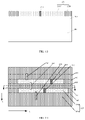
- FIGS. 1-6 illustrate schematic views of semiconductor structures at certain stages of a fabrication process of a semiconductor device
- FIGS. 7-23 illustrate schematic views of semiconductor structures at certain stages of an exemplary method for fabricating a semiconductor device consistent with some embodiments of the present disclosure.
- FIG. 24 illustrates a flowchart of an exemplary method for fabricating a semiconductor device consistent with various embodiments of the present disclosure.
- FIGS. 1-6 illustrate schematic views of semiconductor structures at certain stages of a fabrication process of a semiconductor device.
- the to-be-etched layer 100 includes a plurality of discrete first regions A 01 and a plurality of discrete second regions A 02 .
- the plurality of first regions A 01 and the plurality of second regions A 02 are arranged alternately along a first direction X.
- first region A 01 adjacent to a second region A 02 the first region A 01 and the second region A 02 adjoin each other or in contact with each other.
- Each second region A 02 includes a trench region.
- a first mask layer 110 is formed on the plurality of first regions A 01 and the plurality of second regions A 02 of the to-be-etched layer 100 .
- doping ions are implanted into the first mask layer 110 that is formed outside of the plurality of trench regions, and a plurality of discrete first trenches 120 is formed in the first mask layer 110 of the plurality of first regions A 01 .
- a plurality of discrete separation trenches 130 is formed in the first mask layer 110 of the plurality of second regions A 02 .
- the separation trench 130 divides the first mask layer 110 of the corresponding trench region A 02 into portions arranged in a second direction Y.
- the second direction Y is perpendicular to the first direction X.
- a sidewall spacing layer 140 is formed on the sidewall surfaces of each first trench 120 .
- a separation layer 150 is formed in each separation trench 130 .
- the portion of the first mask layer 110 formed in the trench region on both sides of each separation layer 150 is removed to form a second trench 160 .
- the second trench 160 is located on both sides of the separation layer 150 in the second direction Y.
- the photolithography material e.g., photoresist
- the photolithography material that is used to define the position of the first trench 120 needs to be filled into the separation trench 130 , which leads to an adverse exposing process for the photolithography material in defining the position of the first trench 120 . Therefore, the performance of the semiconductor device fabricated through either process described above may be undesired.
- the present disclosure provides a method for forming semiconductor devices.
- the method includes providing a substrate including a plurality of first regions and a plurality of second regions that are arranged alternately along a first direction with the plurality of second regions including a plurality of trench regions; forming a first mask layer on the substrate; implanting doping ions into the first mask layer formed outside of the plurality of trench regions; forming a plurality of discrete doped separation layers in the first mask layer of the plurality of second regions with each doped separation layer dividing the first mask layer of a corresponding trench region into portions arranged in a second direction perpendicular to the first direction; after implanting the doping ions into the first mask layer formed outside of the plurality of trench regions and forming the plurality of doped separation layers, forming a plurality of first trenches in the first mask layer of the plurality of first regions; after forming the plurality of first trenches, removing the portion of the first mask layer formed in the trench region on both sides of each doped separation layer to form
- FIG. 24 illustrates a flowchart of an exemplary method for fabricating a semiconductor device consistent with various embodiments of the present disclosure.
- FIGS. 7-23 illustrate schematic views of semiconductor structures at certain stages of the exemplary method.
- a to-be-etched layer may be provided, the to-be-etched layer may include a plurality of discrete first regions and a plurality of discrete second regions that are arranged alternately along a first direction, and the plurality of second regions may include a plurality of trench regions (S 401 ).
- FIG. 7 illustrates a schematic top view of a semiconductor structure consistent with various embodiments of the present disclosure.
- a to-be-etched layer 200 may be provided.
- the to-be-etched layer 200 may include a plurality of discrete first regions A 1 and a plurality of discrete second regions A 2 .
- the plurality of first regions A 1 and the plurality of second regions A 2 may be arranged alternately along a first direction X.
- first region A 1 and the second region A 2 may adjoin each other or in contact with each other.
- the plurality of first regions A 1 may be arranged along the first direction X, and the plurality of second regions A 2 may also be arranged along the first direction X.
- the plurality of first regions A 1 and the plurality of second regions A 2 arranged alternatively along the first direction X may refer to that only one second region A 2 may be located between two adjacent first regions A 1 , and only one first region A 1 may be located between two adjacent second regions A 2 .
- the plurality of second regions A 2 includes a plurality of trench regions. That is, in the plurality of second regions A 2 , the to-be-etched layer 200 includes a plurality of trench regions.
- the plurality of trench regions may be used to define the position of a plurality of second trenches that may be formed in a subsequent process.
- Each trench region may adjoin the adjacent first regions, e.g., a trench region may share an edge with each first region A 1 adjacent to the trench region.
- the trench region may be located on a side of the adjacent first region A 1 along the first direction X, e.g. the edge shared by the trench region and the first region A 1 may be perpendicular to the first direction X.
- the total number of the first regions may equal to the total number of the second regions.
- the to-be-etched layer 200 may be made of a material including silicon oxide or a low-k dielectric material (e.g., a material with a relative dielectric constant k smaller than or equal to 3.9).
- FIGS. 8-9 illustrate schematic views of a semiconductor structure consistent with various embodiments of the present disclosure. Specifically, FIG. 8 shows the semiconductor structure from a view direction consistent with that in FIG. 7 , that is, FIG. 8 illustrates a schematic top view of the semiconductor structure; and FIG. 9 illustrates a schematic cross-sectional view of the semiconductor structure shown in FIG. 8 in an M-N direction.
- a first mask layer 220 may be formed on the to-be-etched layer 200 in both the plurality of first regions A 1 and the plurality of second regions A 2 .
- the first mask layer 220 may be made of a material including amorphous silicon.
- the method may further include forming a first adhesion layer (not shown) on the to-be-etched layer 200 ; forming a bottom hard mask layer 210 on the first adhesion layer; and forming a second adhesion layer (not shown) on the bottom hard mask layer 210 . Therefore, the first mask layer 220 may be formed on the second adhesion layer.
- the bottom hard mask layer 210 may be made of a material including titanium nitride.
- the material used for forming the first adhesion layer may include SiOC, and the material used for forming the second adhesion layer may include SiOC.
- the first adhesion layer may be used to improve the adhesion between the bottom hard mask layer 210 and the to-be-etched layer 200 , such that the bonding between the bottom hard mask layer 210 and the to-be-etched layer 200 may be stronger.
- the second adhesion layer may be used to improve the adhesion between the first mask layer 220 and the bottom hard mask layer 210 , such that the bonding between the first mask layer 220 and the bottom hard mask layer 210 may be stronger.
- the function of the bottom hard mask layer 210 may also include the following aspects.
- the bottom hard mask layer 210 may be used as an etch stop layer, e.g., the bottom hard mask layer 210 may be used as a stop layer during a subsequently performed planarization process on a conductive film.
- the bottom hard mask layer 210 may be made of a hard mask material, such that during subsequent formation of a plurality of first target trenches and a plurality of second target trenches, the etching loss of the bottom hard mask layer 210 may be limited. Therefore, during the process of transferring the pattern in the bottom hard mask layer 210 to the to-be-etched layer 200 , the pattern transfer may demonstrate high stability.
- the bottom hard mask layer 210 and the first mask layer 220 may be made of different materials. In other embodiments, the fabrication method may not include forming the bottom hard mask layer, the first adhesion layer, and the second adhesion layer.
- the fabrication method may further include implanting doping ions into the first mask layer in a region outside of the plurality of trench regions.
- a plurality of doped separation layers may be formed in the plurality of second regions A 2 of the first mask layer 220 .
- Each doped separation layer may divide the first mask layer of a corresponding trench region into portions arranged in a second direction (not labeled), and the second direction may be perpendicular to the first direction X.
- doping ions may be implanted into the first mask layer 220 outside of the plurality of trench regions, and then the plurality of doped separation layers may then be formed in the first mask layer 220 of the plurality of second regions.
- the plurality of doped separation layers may be formed in the first mask layer of the plurality of second regions, and then doping ions may then be implanted into the first mask layer outside of the plurality of trench regions.
- FIGS. 10-11 illustrate schematic views of a semiconductor structure consistent with various embodiments of the present disclosure. Specifically, FIG. 10 shows the semiconductor structure from a view direction consistent with that in FIG. 8 , and FIG. 11 shows the semiconductor structure from a view direction consistent with that in FIG. 9 . That is, FIG. 11 illustrates a schematic cross-sectional view of the semiconductor structure shown in FIG. 10 in an M-N direction.
- doping ions may be implanted into the portion of the first mask layer 220 formed outside of the plurality of trench regions.
- the doping ions may be implanted into the portion of the first mask layer 220 formed in the first regions A 1 , and also into the portion of the first mask layer 220 formed in the second regions A 2 outside of the trench regions.
- the process of implanting doping ions into the portion of the first mask layer 220 formed outside of the plurality of trench regions may include the following exemplary steps.
- a first planarization layer may be formed on the first mask layer 220
- a first bottom anti-reflective layer may be formed on the first planarization layer
- a first photoresist layer (not shown) may be formed and patterned on the first bottom anti-reflective layer.
- the first photoresist layer may cover the portion of the first bottom anti-reflective layer that is formed in the plurality of trench regions.
- the first photoresist layer may expose the portion of the first bottom anti-reflective layer formed in the plurality of first regions A 1 and may also expose the portion of the first bottom anti-reflective layer formed in the plurality of second regions A 2 and surrounding the plurality of trench regions.
- the first bottom anti-reflective layer and the first planarization layer may be etched using the first photoresist layer as an etch mask until the top surface of the first mask layer 220 is exposed.
- doping ions may be implanted into the portion of the first mask layer 220 that is formed outside of the plurality of trench regions using the first photoresist layer as a mask. After implanting doping ions into the portion of the first mask layer 220 that is formed outside of the plurality of trench regions using the first photoresist layer as the mask, the first planarization layer, the first bottom anti-reflective layer, and the first photoresist layer may be removed.
- the first mask layer 220 may be divided into an ion-doped region 220 a and an undoped region 220 b.
- the first photoresist layer may expose the portion of the first mask layer 220 formed in the plurality of first regions A 1 . In other embodiments, the first photoresist layer may partially cover the portion of the first mask layer formed in the plurality of first regions.
- the doping ions may include boron ions and/or arsenic ions.
- the doping ions When implanting the doping ions into the portion of the first mask layer 220 that is formed outside of the plurality of trench regions, due to the blocking of the first mask layer 220 and also because a plurality of first trenches and a plurality of second trenches have not been formed in the first mask layer 220 yet, the doping ions may be well prevented from being implanted into the material layer at the bottom of the first mask layer 220 .
- the surface of the first mask layer 220 may be flat, and thus the first planarization layer, the first bottom anti-reflective layer, and the first photoresist layer may all formed on the desired flat surface of the first mask layer 220 , which may be conducive to the exposure process for patterning the first photoresist layer.
- FIGS. 12-13 illustrate schematic views of a semiconductor structure consistent with various embodiments of the present disclosure. Specifically, FIG. 12 shows the semiconductor structure from a view direction consistent with that in FIG. 10 , and FIG. 13 illustrates a schematic cross-sectional view of the semiconductor structure shown in FIG. 12 in an M 1 -N 1 direction.
- a doped separation layer 240 may be formed in the portion of the first mask layer 220 of the second region A 2 , and the doped separation layer 240 may divide the first mask layer 220 of the trench region into portions arranged in a second direction Y.
- the second direction Y may be perpendicular to the first direction X.
- an ion implantation process may be adopted to implant the doping ions into the portion of the first mask layer 220 in the second region A 2 to form the doped separation layer 240 .
- the doping ions when forming the doped separation layer 240 , may also be implanted into a portion of the first mask layer 220 that is located in the first region A 1 adjacent to the doped separation layer 240 along the first direction X.
- the process of forming the doped separation layer 240 may include the following exemplary steps.
- a second planarization layer may be formed on the first mask layer 220
- a second bottom anti-reflective layer may be formed on the second planarization layer
- a second photoresist layer may be formed and patterned on the second bottom anti-reflective layer.
- a plurality of second lithography openings may be formed in the second photoresist layer. Each second lithography opening may be located on a portion of the trench region, and may also extend to the adjacent first region A 1 along the first direction X.
- the second bottom anti-reflective layer and the second planarization layer at the bottom of each second lithography opening may be etched using the second photoresist layer as an etch mask until the top surface of the first mask layer 220 is exposed.
- doping ions may be implanted into the portion of the first mask layer 220 located at the bottom of the second lithography opening using the second photoresist layer as a mask.
- the second planarization layer, the second bottom anti-reflective layer, and the second photoresist layer may be removed.
- the length direction (e.g., the extending direction) of the second lithography opening may be parallel to the first direction X.
- the width of the second lithography opening in the second direction Y may be used to define the size of the doped separation layer 240 in the second direction Y. Because the size of the doped separation layer 240 in the second direction Y is required to be small, the width of the second lithography opening in the second direction Y may be small.
- the width of the second lithography opening in the second direction Y may be in a range of approximately 20 nm to 60 nm, e.g. 20 nm, 30 nm, 40 nm, 50 nm, 60 nm, etc.
- the size of the second lithography opening in the first direction X may be allowed to be made large, such that the size of the second lithography opening may only need to be limited in the second direction Y, while the size of the second lithography opening in the first direction X may not need to be defined small. As such, the challenge on the photolithography process may be lowered, and the process difficulty may be reduced.
- the size of the second lithography opening in the first direction X may be in a range of approximately 65 nm to 1000 nm, e.g. 80 nm, 100 nm, 200 nm, etc.
- the size of the doped separation layer 240 in the first direction X may be in a range of approximately 10 nm to 60 nm, and the size of the doped separation layer 240 in the second direction Y may be in a range of approximately 10 nm to 40 nm.
- the doping ions may also be implanted into the portion of the first mask layer 220 formed in the plurality of first regions A 1 .
- the doping ions may also be implanted into a portion of the first mask layer 220 that is located in the first region A 1 adjacent to the doped separation layer 240 along the first direction X. As such, the definition of the ion-doped region and the undoped region in the first mask layer 220 may not be affected.
- the process difficulty for forming the doped separation layer 240 may be reduced.
- the doping ions may be prevented from being implanted into the material layer at the bottom of the first mask layer 220 .
- the surface of the first mask layer 220 may be flat, and thus the second planarization layer, the second bottom anti-reflective layer, and the second photoresist layer may all formed on the desired flat surface of the first mask layer 220 , which may be conducive to the exposure process for patterning the second photoresist layer.
- FIGS. 14-15 illustrate schematic views of a semiconductor structure consistent with various embodiments of the present disclosure. Specifically, FIG. 14 shows the semiconductor structure from a view direction consistent with that in FIG. 12 , and FIG. 15 illustrates a schematic cross-sectional view of the semiconductor structure shown in FIG. 14 in an M 2 -N 2 direction.
- a top mask layer 250 may be formed on a portion of the first mask layer 220 that is formed in the plurality of first regions A 1 .
- the projection pattern of the top mask layer 250 on the surface of the first mask layer 220 may divide the first mask layer 220 of the first region A 1 into portions arranged in the second direction Y.
- the distance from the top mask layer 250 to the doped separation layer 240 in the second direction Y may be larger than zero. That is, along the second direction Y, the top mask layer 250 and the doped separation layer 240 may be spaced from each other.
- the distance from the top mask layer 250 formed in the first region A 1 to the doped separation layer 240 formed in the second region A 2 may be larger than zero. That is, for a first region and a second region that are adjacent to each other, the position of the top mask layer 250 formed in the first region A 1 and the position of the doped separation layer 240 formed in the second region A 2 may be spaced from each other along the second direction Y.
- the top mask layer 250 may be made of a material including SiO 2 , SiN, TiO 2 , TiN, AlN, Al 2 O 3 , etc.
- the material of the top mask layer 250 may be different from the material of the first mask layer 220 .
- the width of the top mask layer 250 in the second direction Y may be in a range of approximately 10 nm to 40 nm.
- the top mask layer 250 may also extend along the first direction X to cover a portion of the first mask layer 220 formed in the second region A 2 , such that the size of the top mask layer 250 in the first direction X may be large. Because the size of the top mask layer 250 may only need to be limited in the second direction Y, the process difficulty for forming the top mask layer 250 may be reduced.
- the extending direction (e.g. the length direction) of the top mask layer 250 may be parallel to the first direction X.
- the top mask layer may not be able to extend in the first direction to cover a portion of the first mask layer formed in the second region.
- the process of forming the top mask layer 250 may include the following exemplary steps.
- a block layer (not shown) may be formed on the first mask layer 220 and the doped separation layer 240 .
- a block-layer opening may be formed in the block layer, and the block-layer opening may be located on a portion of the first mask layer 220 formed in the first region A 1 , and may also extend along the first direction to expose a portion of the first mask layer 220 formed in the adjacent second regions A 2 .
- the block-layer opening formed in each first region A 1 may divide the first mask layer 220 formed in the first region A 1 into portions arranged in the second direction Y.
- the top mask layer 250 may then be formed in the block-layer opening. After forming the top mask layer 250 in the block-layer opening, the block layer may be removed.
- the extending direction (e.g., the length direction) of the block-layer opening may be parallel to the first direction X, and the block-layer opening may define the position of the top mask layer 250 .
- the block layer may be made of a material including a carbon-containing organic polymer.
- the process of forming the block layer may include the following exemplary steps.
- a third planarization layer may be formed on the first mask layer 220 and the doped separation layer 240 , a third bottom anti-reflective layer may be formed on the third planarization layer, and a third photoresist layer may be formed and patterned on the third bottom anti-reflective layer.
- a plurality of third lithography openings may be formed in the third photoresist layer.
- the third lithography opening may define the position of the block-layer opening.
- the third bottom anti-reflective layer and the third planarization layer at the bottom of each third lithography opening may be etched using the third photoresist layer as an etch mask until the top surface of the first mask layer 220 is exposed. As such, the remaining portion of the third planarization layer may form the block layer. Further, the third bottom anti-reflective layer and the third photoresist layer may be removed.
- the width of the block-layer opening in the second direction Y may be used to define the size of the top mask layer 250 in the second direction Y. Because the size of the top mask layer 250 in the second direction Y may need to be small, the width of the block-layer opening may also need to be small. For example, in one embodiment, the width of the block-layer opening in the second direction Y may be in a range of approximately 10 nm to 40 nm, e.g., 20 nm, 30 nm, 40 nm, etc.
- the size of the block-layer opening in the first direction X may be large. Therefore, the size of the block-layer opening may only need to be limited in the second direction Y, while the size of the block-layer opening in the first direction X may not need to be defined small.
- the size of each third lithography opening in the first direction X may correspond to the size of the block-layer opening in the first direction X
- the size of each third lithography opening in the second direction Y may correspond to the size of the block-layer opening in the second direction Y. Therefore, the size of the third lithography opening may only need to be limited in the second direction Y, while the size of the third lithography opening in the first direction X may not need to be defined small. As such, the challenge on the photolithography process may be lowered, and the process difficulty may be reduced.
- the size of the third lithography opening in the second direction Y may be in a range of approximately 10 nm to 40 nm, and the size of the third lithography opening in the first direction X may be in a range of approximately 65 nm to 1000 nm, e.g. 80 nm, 100 nm, 200 nm, etc.
- a plurality of first trenches may be formed in the first mask layer of the first regions by removing the portion of the first mask layer in the first region on both sides of the top mask layer using the top mask layer as an etch mask, and during the formation of the first trenches, the portion of the first mask layer covered by the top mask layer in the first region may form a separation mask layer, which divides the first trench into portions arranged in the second direction (S 406 ).
- FIGS. 16-17 illustrate schematic views of a semiconductor structure consistent with various embodiments of the present disclosure. Specifically, FIG. 16 shows the semiconductor structure from a view direction consistent with that in FIG. 14 , and FIG. 17 illustrates a schematic cross-sectional view of the semiconductor structure shown in FIG. 16 in an M 2 -N 2 direction.
- the portion of the first mask layer 220 in the first region A 1 located on both sides of the top mask layer 250 may be partially removed through an etching process using the top mask layer 250 as an etch mask to form a first trench 260 in the first mask layer 220 of the first region A 1 .
- the portion of the first mask layer 220 covered by the top mask layer 250 in the first region A 1 may form a separation mask layer 270 .
- the separation mask layer 270 may divide a corresponding first trench 260 into portions arranged in the second direction Y.
- the portion of the first mask layer 220 located under the top mask layer 250 may become a plurality of discrete separation mask layers 270 . Therefore, the plurality of separation mask layers 270 may be located under the top mask layer 250 .
- the process of forming the plurality of first trenches 260 may include a dry etching process, for example, an anisotropic dry etching process, etc.
- each first trench 260 may be parallel to the second direction Y, and the second direction Y may be perpendicular to the first direction X.
- the width of the first trench 260 in the first direction X may be in a range of approximately 10 nm to 60 nm. Further, along the first direction X, the distance between two adjacent first trenches 260 may be in a range of approximately 10 nm to 60 nm.
- the plurality of first trenches 260 is formed in the first mask layer 220 of the first regions A 1 after implanting the doping ions into the portion of the first mask layer 220 formed outside of the plurality of trench regions and forming the doped separation layer 240 . Therefore, during the dry etching process for forming the plurality of first trenches 260 , the etching rate of the portion of the first mask layer 220 that is implanted with the doping ions may need to be similar to the etching rate of the portion of the first mask layer 220 that is not implanted with the doping ions.
- the doping ions implanted into the first mask layer 220 may have a small or negligible effect on the performance of dry etching the first mask layer 220 . As such, the difficulty of the etching process for forming the plurality of first trenches may be reduced.
- the size of the separation mask layer 270 in the first direction X is defined by the width of the first trench 260 in the first direction X, and the width of the first trench 260 in the first direction X is formed small, the size of the separation mask layer 270 in the first direction X may also be small.
- the size of the separation mask layer 270 in the second direction Y is defined by the size of the top mask layer 250 in the second direction Y, and the size of the top mask layer 250 in the second direction Y is formed small, the size of the separation mask layer 270 in the second direction Y may also be small. Therefore, the size of the separation mask layer 270 may be small in both the first direction X and the second direction Y.
- the size of the separation mask layer 270 in the first direction X may be in a range of approximately 10 nm to 60 nm
- the size of the separation mask layer 270 in the second direction Y may be in a range of approximately 10 nm to 40 nm.
- the top mask layer 250 may be used as a mask when forming the plurality of first trenches 260 . Therefore, when etching the first mask layer 220 of the first regions A 1 to form the first trenches 260 , the portion of the first mask layer 220 in the first regions A 1 and located under the top mask layer 250 may be retained to form a plurality of discrete separation mask layers 270 , and each first trench 260 may be divided into portions arranged in the second direction Y by a corresponding separation mask layer 270 . Because the separation mask layer 270 is formed by a portion of the first mask layer 220 , the bonding strength between the separation mask layer 270 and the bottom material may be strong, and thus the separation mask layer 270 may not easily collapse.
- FIGS. 18-19 illustrate schematic views of a semiconductor structure consistent with various embodiments of the present disclosure. Specifically, FIG. 18 shows the semiconductor structure from a view direction consistent with that in FIG. 16 , FIG. 19 shows the semiconductor structure from a view direction consistent with that in FIG. 17 , and FIG. 19 illustrates a schematic cross-sectional view of the semiconductor structure shown in FIG. 18 in an M 2 -N 2 direction.
- the top mask layer 250 may be removed.
- FIGS. 20-21 illustrate schematic views of a semiconductor structure consistent with various embodiments of the present disclosure. Specifically, FIG. 20 shows the semiconductor structure from a view direction consistent with that in FIG. 18 , FIG. 21 shows the semiconductor structure from a view direction consistent with that in FIG. 19 , and FIG. 21 illustrates a schematic cross-sectional view of the semiconductor structure shown in FIG. 20 in an M 2 -N 2 direction.
- a sidewall spacing layer 280 may be formed on the sidewall surfaces of each first trench 260 .
- the sidewall spacing layer 280 may be formed after removing the top mask layer 250 .
- the sidewall spacing layer 280 may be made of a material including SiO 2 , SiN, TiO 2 , TiN, AlN, or Al 2 O 3 .
- the material of the sidewall spacing layer 280 may be different from the material of the first mask layer.
- the material of the sidewall spacing layer 280 may be different from the material of the first mask layer not implanted with the doping ions.
- the thickness of the sidewall spacing layer 280 may be in a range of approximately 10 nm to 25 nm.
- the process of forming the sidewall spacing layer 280 may include the following exemplary steps.
- a sidewall film layer may be formed on the sidewall and bottom surfaces of the first trench 260 and also on the top surface of the first mask layer 220 .
- the sidewall film layer may then be etched back to expose the top surface of the first mask layer 220 .
- the process adopted for forming the sidewall film layer may be a deposition process such as an atomic layer deposition (ALD) process.
- ALD atomic layer deposition
- the sidewall surfaces of the separation mask layer 270 that are perpendicular to the second direction Y may also be covered by the sidewall spacing layer 280 .
- the sidewall spacing layer 280 formed on the sidewall surfaces of the separation mask layer 270 may provide protection for the separation mask layer 270 , and thus in the subsequent process of forming the plurality of second trenches, the separation mask layer 270 may not easily collapse.
- FIGS. 22-23 illustrate schematic views of a semiconductor structure consistent with various embodiments of the present disclosure. Specifically, FIG. 22 shows the semiconductor structure from a view direction consistent with that in FIG. 20 , and FIG. 23 illustrates a schematic cross-sectional view of the semiconductor structure shown in FIG. 22 in an M 1 -N 1 direction.
- the portion of the first mask layer 220 formed in the trench region on both sides of the doped separation layer 240 may be removed through etching to form a second trench 290 in the first mask layer 220 of the second region A 2 .
- the doped separation layer 240 may divide the second trench 290 into portions arranged in the second direction Y.
- the second trench 290 may be formed after forming the sidewall spacing layer 280 .
- the sidewall spacing layer 280 may be exposed in the second trench 290 and thus may serve as a portion of the sidewalls of the second trench 290 .
- the second trench 290 may be separated from an adjacent first trench 260 by the sidewall spacing layer 280 .
- removing the portion of the first mask layer 220 formed in the trench region on both sides of the doped separation layer 240 may include a wet etching process.
- the etching rate of the portion of the first mask layer 220 not implanted with the doping ions may be greater than the etching rate of the portion of the first mask layer 220 implanted with the doping ions.
- the etching rate of the undoped region 220 b may be a first etching rate
- the etching rate of the doped region 220 a may be a second etching rate
- the ratio of the first etching rate to the second etching rate may be larger than or equal to approximately 100, e.g. 150.
- the process for removing the portion of the first mask layer 220 formed in the trench region on both sides of the doped separation layer 240 may be prevented from etching through the sidewall spacing layer 280 and causing penetration between the first trench and the adjacent second trench.
- the doped separation layer 240 may not be etched and removed during the process of removing the portion of the first mask layer 220 formed in the trench region on both sides of the doped separation layer 240 .
- the extending direction (e.g., the length direction) of the second trench 290 may be parallel to the second direction Y.
- the width of the second trench 290 in the first direction X may be in a range of approximately 10 nm to 60 nm.
- the surfaces of the first mask layer 220 and the doped separation layer 240 may be flat, which may be conducive to the exposure process for patterning the photolithography material to define the position of the first trench 260 .
- the fabrication method may also include etching the portion of the to-be-etched layer 200 at the bottom of the first trench 260 to form a first target trench in the to-be-etched layer 200 ; etching the portion of the to-be-etched layer 200 at the bottom of the second trench 290 to form a second target trench in the to-be-etched layer 200 ; forming a first conductive layer in the first target trench; and forming a second conductive layer in the second target trench.
- the fabrication method may also include etching the portion of the second adhesion layer, the bottom hard mask layer 210 , and the first adhesion layer at the bottom of the first trench 260 to form a first hard mask trench in the bottom hard mask layer 210 at the bottom of the first trench 260 ; and etching the portion of the second adhesion layer, the bottom hard mask layer 210 , and the first adhesion layer at the bottom of the second trench 290 to form a second hard mask trench in the bottom hard mask layer 210 at the bottom of the second trench 290 .
- the first mask layer 220 and the second adhesion layer may be removed.
- the portion of the to-be-etch layer 200 at the bottom of the first hard mask trench may be etched to form a first target trench in the to-be-etched layer 200 .
- the portion of the to-be-etch layer 200 at the bottom of the second hard mask trench may be etched to form a second target trench in the to-be-etched layer 200 .
- a conductive film layer may be formed in the first target trench and the second target trench and also on the bottom hard mask layer 210 .
- the conductive film layer may be planarized until the top surface of the bottom hard mask layer 210 is exposed, such that a first conductive layer may be formed in the first target trench and a second conductive layer may be formed in the second target trench. Further, the bottom hard mask layer 210 and the first adhesion layer may be removed.
- the first conductive layer and the second conductive layer may be both made of a metal, e.g. copper, aluminum, etc.
- FIGS. 22-23 illustrate schematic views of an exemplary semiconductor device consistent with various embodiments of the present disclosure. Specifically, FIG. 22 illustrates a schematic top view of the semiconductor device and FIG. 23 illustrates a schematic cross-sectional view of the semiconductor device shown in FIG. 22 in the M 1 -N 1 direction.
- the semiconductor device may include a to-be-etched layer 200 .
- the to-be-etched layer 200 may include a plurality of discrete first regions A 1 and a plurality of discrete second regions A 2 .
- the plurality of first regions A 1 and the plurality of second regions A 2 may be arranged alternately along a first direction X.
- first region A 1 adjacent to a second region A 2 the first region A 1 and the second region A 2 may adjoin each other, e.g., the first region A 1 and the second region A 2 may share an edge.
- the plurality of first regions A 1 may be arranged along the first direction X, and the plurality of second regions may be arranged along the first direction X.
- the plurality of first regions A 1 and the plurality of second regions A 2 arranged alternatively along the first direction X may refer to that only one second region A 2 may be located between two adjacent first regions A 1 , and only one first region A 1 may be located between two adjacent second regions A 2 .
- the semiconductor device may include a first mask layer (not labeled) formed on the to-be-etched layer 200 , a plurality of first trenches 260 formed in the first mask layer of the first regions A 1 , and a plurality of second trenches 290 formed in the first mask layer of the second regions A 2 .
- the first mask layer may be implanted with a plurality of doping ions, and thus the first mask layer may include an ion-doped region 220 a .
- the doping ions implanted into the ion-doped region 220 a of the first mask layer may include boron ions and/or arsenic ions.
- the semiconductor device may also include a bottom hard mask layer 210 formed between the to-be-etched layer 200 and the first mask layer, a first adhesion layer formed between the bottom hard mask layer 210 and the to-be-etched layer 200 , and a second adhesion layer formed between the bottom hard mask layer and the first mask layer.
- the first adhesion layer may be used to improve the adhesion between the bottom hard mask layer 210 and the to-be-etched layer 200 , such that the bonding between the bottom hard mask layer 210 and the to-be-etched layer 200 may be stronger.
- the second adhesion layer may be used to improve the adhesion between the first mask layer and the bottom hard mask layer 210 , such that the bonding between the first mask layer and the bottom hard mask layer 210 may be stronger.
- the plurality of first trenches 260 and the plurality of second trenches 290 may expose the top surface of the bottom hard mask layer.
- each first trench 260 may be divided into portions arranged in a second direction Y by a separation mask layer 270
- each second trench 290 may be divided into portions arranged in the second direction Y by a doped separation layer 240 .
- the second direction Y may be perpendicular to the first direction X.
- the semiconductor device may include a sidewall spacing layer 280 serving as the sidewalls of each first trench 260 .
- the sidewall spacing layer 280 may also cover the sidewall surfaces of the separation mask layer 270 .
- each first trench 260 may be separated from an adjacent second trench 290 by a sidewall spacing layer 280 .
- the size of the doped separation layer 240 in the first direction X may be in a range of approximately 10 nm to 60 nm, and the size of the doped separation layer 240 in the second direction Y may be in a range of approximately 10 nm to 40 nm.
- the width of the first trench 260 in the first direction X may be in a range of approximately 10 nm to 60 nm. Further, along the first direction X, the distance between two adjacent first trenches 260 may be in a range of approximately 10 nm to 60 nm.
- the size of the separation mask layer 270 in the first direction X may be in a range of approximately 10 nm to 60 nm
- the size of the separation mask layer 270 in the second direction Y may be in a range of approximately 10 nm to 40 nm.
- the thickness of the sidewall spacing layer 280 may be in a range of approximately 10 nm to 25 nm.
- the extending direction (e.g., the length direction) of the second trench 290 may be parallel to the second direction Y.
- the width of the second trench 290 in the first direction X may be in a range of approximately 10 nm to 60 nm.
- the disclosed semiconductor device and fabrication method may demonstrate the following exemplary advantages.
- doping ions are implanted into the first mask layer formed outside of the trench regions, and a plurality of doped separation layers are formed in the first mask layer of the second regions. Therefore, the material of the first mask layer in the trench regions on both sides of each doped separation layer is different from the material of the doped separation layer, and the material of the first mask layer in the trench regions on both sides of each doped separation layer is also different from the material of the first mask layer formed outside of the trench regions. As such, by removing the portion of the first mask layer on both sides of the doped separation layer, a second trench is formed.
- implanting the doping ions into the first mask layer outside of the trench regions and forming the doped separation layer are both completed prior to forming the plurality of first trenches, and the surface of the first mask layer is flat during the process of forming the doped separation layer. Therefore, the photolithography material used to define the position of the doped separation layer can be avoided from being formed in the first trench.
- the photolithography material used to define the position of the doped separation layer can be formed on the desired flat surface of the first mask layer, which is conducive to the exposure process for patterning the photolithography material.
- the photolithography material used when implanting the doping ions into the first mask layer outside of the trench regions can be avoided from being formed in the first trench, which is conducive to the exposure process for patterning the photolithography material.
- the surfaces of the first mask layer and the doped separation layer are flat, thereby conducive to the exposure process for patterning the photolithography material to define the position of the first trench. As such, the disclosed fabrication method improves the performance of the formed semiconductor device.
- a top mask layer is used as a mask, thereby during the process of etching the first mask layer to form a first trench in the first region, the portion of the first mask layer in the first region and located under the top mask layer is retained to form the separation mask layer. Therefore, each first trench is thus divided into portions arranged in the second direction by the separation mask layer. Because the separation mask layer is formed from a portion of the first mask layer, the bonding strength between the separation mask layer and the bottom material may be strong, and thus the separation mask layer may not easily collapse.
- a sidewall spacing layer is formed on the sidewall surfaces of the first trench.
- the sidewall spacing layer may also be formed on the two sidewall surfaces of the separation mask layer in the second direction. Therefore, the sidewall spacing layer formed on the sidewall surfaces of the separation mask layer is able to provide protection for the separation mask layer, such that during the process of forming the second trench, the separation mask layer may not easily collapse.
- the doping ions are also implanted into the first mask layer of the first region.
- doping ions are also implanted into the portion of the first mask layer that is located in the first region adjacent to the doped separation layer along the first direction.
- the definition of the ion-doped region and the undoped region in the first mask layer may not be affected. Because the doping ions are implanted into the portion of the first mask layer that is located in the first region adjacent to the doped separation layer along the first direction during the process of forming the doped separation layer, the process difficulty for forming the doped separation layer may be reduced.
Abstract
Description
Claims (18)
Applications Claiming Priority (2)
| Application Number | Priority Date | Filing Date | Title |
|---|---|---|---|
| CN201910156244.1A CN111640659B (en) | 2019-03-01 | 2019-03-01 | Semiconductor device and method of forming the same |
| CN201910156244.1 | 2019-03-01 |
Publications (2)
| Publication Number | Publication Date |
|---|---|
| US20200279741A1 US20200279741A1 (en) | 2020-09-03 |
| US11430657B2 true US11430657B2 (en) | 2022-08-30 |
Family
ID=72236919
Family Applications (1)
| Application Number | Title | Priority Date | Filing Date |
|---|---|---|---|
| US16/804,192 Active 2040-07-31 US11430657B2 (en) | 2019-03-01 | 2020-02-28 | Semiconductor devices and fabrication methods thereof |
Country Status (2)
| Country | Link |
|---|---|
| US (1) | US11430657B2 (en) |
| CN (1) | CN111640659B (en) |
Families Citing this family (2)
| Publication number | Priority date | Publication date | Assignee | Title |
|---|---|---|---|---|
| CN111640666B (en) * | 2019-03-01 | 2023-06-13 | 中芯国际集成电路制造(上海)有限公司 | Semiconductor device and method of forming the same |
| CN111834212B (en) * | 2019-04-23 | 2023-05-26 | 中芯国际集成电路制造(上海)有限公司 | Semiconductor device and method of forming the same |
Citations (6)
| Publication number | Priority date | Publication date | Assignee | Title |
|---|---|---|---|---|
| US20080132073A1 (en) * | 2006-12-04 | 2008-06-05 | Hynix Semiconductor Inc. | Oxide Pattern Forming Method and Patterning Method of Semiconductor Device |
| US20140273461A1 (en) * | 2013-03-15 | 2014-09-18 | Applied Materials, Inc. | Carbon film hardmask stress reduction by hydrogen ion implantation |
| US20190027365A1 (en) * | 2016-01-26 | 2019-01-24 | Micron Technology, Inc. | Methods of patterning a target layer |
| US10714343B1 (en) * | 2019-02-02 | 2020-07-14 | Semiconductor Manufacturing (Shanghai) International Corporation | Semiconductor structure and method for forming same |
| US20200279738A1 (en) * | 2019-03-01 | 2020-09-03 | Semiconductor Manufacturing International (Shanghai) Corporation | Semiconductor devices and fabrication methods thereof |
| US20200279740A1 (en) * | 2019-03-01 | 2020-09-03 | Semiconductor Manufacturing International (Shanghai) Corporation | Semiconductor device and fabrication method thereof |
Family Cites Families (2)
| Publication number | Priority date | Publication date | Assignee | Title |
|---|---|---|---|---|
| CN104347477B (en) * | 2013-07-24 | 2018-06-01 | 中芯国际集成电路制造(上海)有限公司 | The forming method of semiconductor structure |
| CN105719956B (en) * | 2014-12-04 | 2019-05-28 | 中芯国际集成电路制造(上海)有限公司 | The forming method of semiconductor structure |
-
2019
- 2019-03-01 CN CN201910156244.1A patent/CN111640659B/en active Active
-
2020
- 2020-02-28 US US16/804,192 patent/US11430657B2/en active Active
Patent Citations (6)
| Publication number | Priority date | Publication date | Assignee | Title |
|---|---|---|---|---|
| US20080132073A1 (en) * | 2006-12-04 | 2008-06-05 | Hynix Semiconductor Inc. | Oxide Pattern Forming Method and Patterning Method of Semiconductor Device |
| US20140273461A1 (en) * | 2013-03-15 | 2014-09-18 | Applied Materials, Inc. | Carbon film hardmask stress reduction by hydrogen ion implantation |
| US20190027365A1 (en) * | 2016-01-26 | 2019-01-24 | Micron Technology, Inc. | Methods of patterning a target layer |
| US10714343B1 (en) * | 2019-02-02 | 2020-07-14 | Semiconductor Manufacturing (Shanghai) International Corporation | Semiconductor structure and method for forming same |
| US20200279738A1 (en) * | 2019-03-01 | 2020-09-03 | Semiconductor Manufacturing International (Shanghai) Corporation | Semiconductor devices and fabrication methods thereof |
| US20200279740A1 (en) * | 2019-03-01 | 2020-09-03 | Semiconductor Manufacturing International (Shanghai) Corporation | Semiconductor device and fabrication method thereof |
Also Published As
| Publication number | Publication date |
|---|---|
| CN111640659A (en) | 2020-09-08 |
| CN111640659B (en) | 2023-04-25 |
| US20200279741A1 (en) | 2020-09-03 |
Similar Documents
| Publication | Publication Date | Title |
|---|---|---|
| US11251044B2 (en) | Semiconductor devices and fabrication methods thereof | |
| CN111640656B (en) | Semiconductor device and method of forming the same | |
| US20220319863A1 (en) | Semiconductor device and fabrication method thereof | |
| US11769691B2 (en) | Semiconductor device and formation method thereof | |
| US11430657B2 (en) | Semiconductor devices and fabrication methods thereof | |
| EP3267474A1 (en) | Contact structure and associated method for flash memory | |
| US11335560B2 (en) | Semiconductor devices and fabrication methods thereof | |
| US20200279737A1 (en) | Semiconductor device and fabrication method thereof | |
| KR102327667B1 (en) | Methods of manufacturing semiconductor devices | |
| US11183395B2 (en) | Semiconductor device and fabrication method thereof | |
| CN111640665B (en) | Semiconductor device and method of forming the same | |
| CN111640664B (en) | Semiconductor device and method of forming the same | |
| CN111668093B (en) | Semiconductor device and method of forming the same | |
| CN111640667B (en) | Semiconductor device and method of forming the same | |
| CN111668155B (en) | Patterning method and semiconductor device formed thereby | |
| CN111640653B (en) | Semiconductor structure and forming method thereof | |
| CN111668156B (en) | Patterning method and semiconductor device formed thereby | |
| CN112053947B (en) | Patterning method and semiconductor device formed thereby | |
| CN111668099B (en) | Patterning method and semiconductor device formed thereby | |
| US11894231B2 (en) | Semiconductor fabrication method and structure using multiple sacrificial layers to form sidewall spacers | |
| CN111952170B (en) | Semiconductor device and method of forming the same | |
| CN111952154A (en) | Patterning method and semiconductor device formed by same | |
| US20090053873A1 (en) | Method of forming semiconductor structure |
Legal Events
| Date | Code | Title | Description |
|---|---|---|---|
| AS | Assignment |
Owner name: SEMICONDUCTOR MANUFACTURING INTERNATIONAL (BEIJING) CORPORATION, CHINA Free format text: ASSIGNMENT OF ASSIGNORS INTEREST;ASSIGNORS:SHI, WEI;HU, YOUCUN;REEL/FRAME:051959/0786 Effective date: 20200214 Owner name: SEMICONDUCTOR MANUFACTURING INTERNATIONAL (SHANGHAI) CORPORATION, CHINA Free format text: ASSIGNMENT OF ASSIGNORS INTEREST;ASSIGNORS:SHI, WEI;HU, YOUCUN;REEL/FRAME:051959/0786 Effective date: 20200214 |
|
| FEPP | Fee payment procedure |
Free format text: ENTITY STATUS SET TO UNDISCOUNTED (ORIGINAL EVENT CODE: BIG.); ENTITY STATUS OF PATENT OWNER: LARGE ENTITY |
|
| STPP | Information on status: patent application and granting procedure in general |
Free format text: DOCKETED NEW CASE - READY FOR EXAMINATION |
|
| STPP | Information on status: patent application and granting procedure in general |
Free format text: NON FINAL ACTION MAILED |
|
| STPP | Information on status: patent application and granting procedure in general |
Free format text: RESPONSE TO NON-FINAL OFFICE ACTION ENTERED AND FORWARDED TO EXAMINER |
|
| STPP | Information on status: patent application and granting procedure in general |
Free format text: EX PARTE QUAYLE ACTION MAILED |
|
| STPP | Information on status: patent application and granting procedure in general |
Free format text: RESPONSE TO EX PARTE QUAYLE ACTION ENTERED AND FORWARDED TO EXAMINER |
|
| STPP | Information on status: patent application and granting procedure in general |
Free format text: NOTICE OF ALLOWANCE MAILED -- APPLICATION RECEIVED IN OFFICE OF PUBLICATIONS |
|
| STPP | Information on status: patent application and granting procedure in general |
Free format text: PUBLICATIONS -- ISSUE FEE PAYMENT VERIFIED |
|
| STCF | Information on status: patent grant |
Free format text: PATENTED CASE |