US11415885B2 - Semiconductor photoresist composition, and method of forming patterns using the composition - Google Patents
Semiconductor photoresist composition, and method of forming patterns using the composition Download PDFInfo
- Publication number
- US11415885B2 US11415885B2 US17/036,693 US202017036693A US11415885B2 US 11415885 B2 US11415885 B2 US 11415885B2 US 202017036693 A US202017036693 A US 202017036693A US 11415885 B2 US11415885 B2 US 11415885B2
- Authority
- US
- United States
- Prior art keywords
- group
- substituted
- photoresist composition
- semiconductor photoresist
- unsubstituted
- Prior art date
- Legal status (The legal status is an assumption and is not a legal conclusion. Google has not performed a legal analysis and makes no representation as to the accuracy of the status listed.)
- Active
Links
- 0 [1*][Sn]1(C)OC(=O)CC(=O)O1.[2*][Sn](C)(C)OC(=O)CC(=O)O[Sn]([3*])(C)C.[4*][Sn]1(OC(=O)CC(=O)O[Sn]2([5*])OC(=O)CC(=O)O2)OC(=O)CC(=O)O1 Chemical compound [1*][Sn]1(C)OC(=O)CC(=O)O1.[2*][Sn](C)(C)OC(=O)CC(=O)O[Sn]([3*])(C)C.[4*][Sn]1(OC(=O)CC(=O)O[Sn]2([5*])OC(=O)CC(=O)O2)OC(=O)CC(=O)O1 0.000 description 4
- YMDKYQQFCLJZJR-UHFFFAOYSA-H CC(C)[Sn]1(OC(=O)CC(=O)O[Sn]2(C(C)C)OC(=O)CC(=O)O2)OC(=O)CC(=O)O1 Chemical compound CC(C)[Sn]1(OC(=O)CC(=O)O[Sn]2(C(C)C)OC(=O)CC(=O)O2)OC(=O)CC(=O)O1 YMDKYQQFCLJZJR-UHFFFAOYSA-H 0.000 description 1
- RPFBMJCLNLQILE-UHFFFAOYSA-H CC(C)[Sn]1(OC(=O)CCC(=O)O[Sn]2(C(C)C)OC(=O)CCC(=O)O2)OC(=O)CCC(=O)O1 Chemical compound CC(C)[Sn]1(OC(=O)CCC(=O)O[Sn]2(C(C)C)OC(=O)CCC(=O)O2)OC(=O)CCC(=O)O1 RPFBMJCLNLQILE-UHFFFAOYSA-H 0.000 description 1
- UEHDYWMZBHMYTR-UHFFFAOYSA-H CCC(=O)O[Sn](Cc1ccccc1)(OC(=O)CC)OC(=O)CC(=O)O[Sn](Cc1ccccc1)(OC(=O)CC)OC(=O)CC Chemical compound CCC(=O)O[Sn](Cc1ccccc1)(OC(=O)CC)OC(=O)CC(=O)O[Sn](Cc1ccccc1)(OC(=O)CC)OC(=O)CC UEHDYWMZBHMYTR-UHFFFAOYSA-H 0.000 description 1
- CXUXZKSFMICETJ-UHFFFAOYSA-H CCC(=O)O[Sn](OC(=O)CC)(OC(=O)CC(=O)O[Sn](OC(=O)CC)(OC(=O)CC)C(C)C)C(C)C Chemical compound CCC(=O)O[Sn](OC(=O)CC)(OC(=O)CC(=O)O[Sn](OC(=O)CC)(OC(=O)CC)C(C)C)C(C)C CXUXZKSFMICETJ-UHFFFAOYSA-H 0.000 description 1
- GRGJXZYSUZULJQ-UHFFFAOYSA-H CCC(=O)O[Sn](OC(=O)CC)(OC(=O)CCC(=O)O[Sn](OC(=O)CC)(OC(=O)CC)C(C)C)C(C)C Chemical compound CCC(=O)O[Sn](OC(=O)CC)(OC(=O)CCC(=O)O[Sn](OC(=O)CC)(OC(=O)CC)C(C)C)C(C)C GRGJXZYSUZULJQ-UHFFFAOYSA-H 0.000 description 1
- BKFIWPUPGCTZMW-UHFFFAOYSA-K CCC(=O)O[Sn]1(C(C)C)OC(=O)CC(=O)O1 Chemical compound CCC(=O)O[Sn]1(C(C)C)OC(=O)CC(=O)O1 BKFIWPUPGCTZMW-UHFFFAOYSA-K 0.000 description 1
- KSUJGGPEXHVWRT-UHFFFAOYSA-K CCC(=O)O[Sn]1(C(C)C)OC(=O)CCC(=O)O1 Chemical compound CCC(=O)O[Sn]1(C(C)C)OC(=O)CCC(=O)O1 KSUJGGPEXHVWRT-UHFFFAOYSA-K 0.000 description 1
- KSGNJSMSKWHZQQ-UHFFFAOYSA-K CCC(=O)O[Sn]1(c2ccccc2)OC(=O)CC(=O)O1 Chemical compound CCC(=O)O[Sn]1(c2ccccc2)OC(=O)CC(=O)O1 KSGNJSMSKWHZQQ-UHFFFAOYSA-K 0.000 description 1
- RCDWLFAUSVRVCF-UHFFFAOYSA-N CCO[Sn](CC(C)(C)C)(OCC)OCC Chemical compound CCO[Sn](CC(C)(C)C)(OCC)OCC RCDWLFAUSVRVCF-UHFFFAOYSA-N 0.000 description 1
- FPCBLJHXRNZOCC-UHFFFAOYSA-N c1cc2c3c(c1)ccc1ccc4cccc-2c4c13.c1cc2ccc3ccc4ccc5ccc6ccc1c1c2c3c4c5c61.c1cc2ccc3ccc4ccc5cccc6c(c1)c2c3c4c56.c1cc2ccc3cccc4ccc(c1)c2c34.c1cc2cccc3c4cccc5cccc(c(c1)c23)c54.c1ccc(-c2ccccc2)cc1.c1ccc2c(c1)-c1cccc3cccc-2c13.c1ccc2c(c1)cc1ccc3cccc4ccc2c1c34.c1ccc2c(c1)cc1cccc3c4cccc5cccc(c54)c2c13.c1ccc2c(c1)ccc1c3ccccc3ccc21.c1ccc2c(c1)ccc1ccc3ccccc3c12.c1ccc2c(c1)ccc1ccccc12.c1ccc2c3c4c(ccc5ccc6cccc-3c6c54)cc2c1.c1ccc2cc3ccccc3cc2c1.c1ccc2ccccc2c1.c1ccccc1 Chemical compound c1cc2c3c(c1)ccc1ccc4cccc-2c4c13.c1cc2ccc3ccc4ccc5ccc6ccc1c1c2c3c4c5c61.c1cc2ccc3ccc4ccc5cccc6c(c1)c2c3c4c56.c1cc2ccc3cccc4ccc(c1)c2c34.c1cc2cccc3c4cccc5cccc(c(c1)c23)c54.c1ccc(-c2ccccc2)cc1.c1ccc2c(c1)-c1cccc3cccc-2c13.c1ccc2c(c1)cc1ccc3cccc4ccc2c1c34.c1ccc2c(c1)cc1cccc3c4cccc5cccc(c54)c2c13.c1ccc2c(c1)ccc1c3ccccc3ccc21.c1ccc2c(c1)ccc1ccc3ccccc3c12.c1ccc2c(c1)ccc1ccccc12.c1ccc2c3c4c(ccc5ccc6cccc-3c6c54)cc2c1.c1ccc2cc3ccccc3cc2c1.c1ccc2ccccc2c1.c1ccccc1 FPCBLJHXRNZOCC-UHFFFAOYSA-N 0.000 description 1
- SXWABYGOCBOCCL-UHFFFAOYSA-N c1ccc2cc3cc4cc5ccccc5cc4cc3cc2c1.c1ccc2cc3cc4ccccc4cc3cc2c1 Chemical compound c1ccc2cc3cc4cc5ccccc5cc4cc3cc2c1.c1ccc2cc3cc4ccccc4cc3cc2c1 SXWABYGOCBOCCL-UHFFFAOYSA-N 0.000 description 1
Images


Classifications
-
- G—PHYSICS
- G03—PHOTOGRAPHY; CINEMATOGRAPHY; ANALOGOUS TECHNIQUES USING WAVES OTHER THAN OPTICAL WAVES; ELECTROGRAPHY; HOLOGRAPHY
- G03F—PHOTOMECHANICAL PRODUCTION OF TEXTURED OR PATTERNED SURFACES, e.g. FOR PRINTING, FOR PROCESSING OF SEMICONDUCTOR DEVICES; MATERIALS THEREFOR; ORIGINALS THEREFOR; APPARATUS SPECIALLY ADAPTED THEREFOR
- G03F7/00—Photomechanical, e.g. photolithographic, production of textured or patterned surfaces, e.g. printing surfaces; Materials therefor, e.g. comprising photoresists; Apparatus specially adapted therefor
- G03F7/004—Photosensitive materials
- G03F7/0042—Photosensitive materials with inorganic or organometallic light-sensitive compounds not otherwise provided for, e.g. inorganic resists
-
- G—PHYSICS
- G03—PHOTOGRAPHY; CINEMATOGRAPHY; ANALOGOUS TECHNIQUES USING WAVES OTHER THAN OPTICAL WAVES; ELECTROGRAPHY; HOLOGRAPHY
- G03F—PHOTOMECHANICAL PRODUCTION OF TEXTURED OR PATTERNED SURFACES, e.g. FOR PRINTING, FOR PROCESSING OF SEMICONDUCTOR DEVICES; MATERIALS THEREFOR; ORIGINALS THEREFOR; APPARATUS SPECIALLY ADAPTED THEREFOR
- G03F7/00—Photomechanical, e.g. photolithographic, production of textured or patterned surfaces, e.g. printing surfaces; Materials therefor, e.g. comprising photoresists; Apparatus specially adapted therefor
- G03F7/004—Photosensitive materials
-
- C—CHEMISTRY; METALLURGY
- C07—ORGANIC CHEMISTRY
- C07F—ACYCLIC, CARBOCYCLIC OR HETEROCYCLIC COMPOUNDS CONTAINING ELEMENTS OTHER THAN CARBON, HYDROGEN, HALOGEN, OXYGEN, NITROGEN, SULFUR, SELENIUM OR TELLURIUM
- C07F7/00—Compounds containing elements of Groups 4 or 14 of the Periodic Table
- C07F7/22—Tin compounds
- C07F7/2224—Compounds having one or more tin-oxygen linkages
-
- G—PHYSICS
- G03—PHOTOGRAPHY; CINEMATOGRAPHY; ANALOGOUS TECHNIQUES USING WAVES OTHER THAN OPTICAL WAVES; ELECTROGRAPHY; HOLOGRAPHY
- G03F—PHOTOMECHANICAL PRODUCTION OF TEXTURED OR PATTERNED SURFACES, e.g. FOR PRINTING, FOR PROCESSING OF SEMICONDUCTOR DEVICES; MATERIALS THEREFOR; ORIGINALS THEREFOR; APPARATUS SPECIALLY ADAPTED THEREFOR
- G03F7/00—Photomechanical, e.g. photolithographic, production of textured or patterned surfaces, e.g. printing surfaces; Materials therefor, e.g. comprising photoresists; Apparatus specially adapted therefor
- G03F7/20—Exposure; Apparatus therefor
- G03F7/2002—Exposure; Apparatus therefor with visible light or UV light, through an original having an opaque pattern on a transparent support, e.g. film printing, projection printing; by reflection of visible or UV light from an original such as a printed image
- G03F7/2012—Exposure; Apparatus therefor with visible light or UV light, through an original having an opaque pattern on a transparent support, e.g. film printing, projection printing; by reflection of visible or UV light from an original such as a printed image using liquid photohardening compositions, e.g. for the production of reliefs such as flexographic plates or stamps
-
- G—PHYSICS
- G03—PHOTOGRAPHY; CINEMATOGRAPHY; ANALOGOUS TECHNIQUES USING WAVES OTHER THAN OPTICAL WAVES; ELECTROGRAPHY; HOLOGRAPHY
- G03F—PHOTOMECHANICAL PRODUCTION OF TEXTURED OR PATTERNED SURFACES, e.g. FOR PRINTING, FOR PROCESSING OF SEMICONDUCTOR DEVICES; MATERIALS THEREFOR; ORIGINALS THEREFOR; APPARATUS SPECIALLY ADAPTED THEREFOR
- G03F7/00—Photomechanical, e.g. photolithographic, production of textured or patterned surfaces, e.g. printing surfaces; Materials therefor, e.g. comprising photoresists; Apparatus specially adapted therefor
- G03F7/20—Exposure; Apparatus therefor
- G03F7/2045—Exposure; Apparatus therefor using originals with apertures, e.g. stencil exposure masks
-
- H01L21/0274—
-
- H01L21/31116—
-
- H01L21/31144—
-
- H01L21/32135—
-
- H01L21/32139—
-
- H—ELECTRICITY
- H10—SEMICONDUCTOR DEVICES; ELECTRIC SOLID-STATE DEVICES NOT OTHERWISE PROVIDED FOR
- H10P—GENERIC PROCESSES OR APPARATUS FOR THE MANUFACTURE OR TREATMENT OF DEVICES COVERED BY CLASS H10
- H10P50/00—Etching of wafers, substrates or parts of devices
- H10P50/20—Dry etching; Plasma etching; Reactive-ion etching
- H10P50/26—Dry etching; Plasma etching; Reactive-ion etching of conductive or resistive materials
- H10P50/264—Dry etching; Plasma etching; Reactive-ion etching of conductive or resistive materials by chemical means
- H10P50/266—Dry etching; Plasma etching; Reactive-ion etching of conductive or resistive materials by chemical means by vapour etching only
-
- H—ELECTRICITY
- H10—SEMICONDUCTOR DEVICES; ELECTRIC SOLID-STATE DEVICES NOT OTHERWISE PROVIDED FOR
- H10P—GENERIC PROCESSES OR APPARATUS FOR THE MANUFACTURE OR TREATMENT OF DEVICES COVERED BY CLASS H10
- H10P50/00—Etching of wafers, substrates or parts of devices
- H10P50/20—Dry etching; Plasma etching; Reactive-ion etching
- H10P50/28—Dry etching; Plasma etching; Reactive-ion etching of insulating materials
- H10P50/282—Dry etching; Plasma etching; Reactive-ion etching of insulating materials of inorganic materials
- H10P50/283—Dry etching; Plasma etching; Reactive-ion etching of insulating materials of inorganic materials by chemical means
-
- H—ELECTRICITY
- H10—SEMICONDUCTOR DEVICES; ELECTRIC SOLID-STATE DEVICES NOT OTHERWISE PROVIDED FOR
- H10P—GENERIC PROCESSES OR APPARATUS FOR THE MANUFACTURE OR TREATMENT OF DEVICES COVERED BY CLASS H10
- H10P50/00—Etching of wafers, substrates or parts of devices
- H10P50/71—Etching of wafers, substrates or parts of devices using masks for conductive or resistive materials
-
- H—ELECTRICITY
- H10—SEMICONDUCTOR DEVICES; ELECTRIC SOLID-STATE DEVICES NOT OTHERWISE PROVIDED FOR
- H10P—GENERIC PROCESSES OR APPARATUS FOR THE MANUFACTURE OR TREATMENT OF DEVICES COVERED BY CLASS H10
- H10P50/00—Etching of wafers, substrates or parts of devices
- H10P50/73—Etching of wafers, substrates or parts of devices using masks for insulating materials
-
- H—ELECTRICITY
- H10—SEMICONDUCTOR DEVICES; ELECTRIC SOLID-STATE DEVICES NOT OTHERWISE PROVIDED FOR
- H10P—GENERIC PROCESSES OR APPARATUS FOR THE MANUFACTURE OR TREATMENT OF DEVICES COVERED BY CLASS H10
- H10P76/00—Manufacture or treatment of masks on semiconductor bodies, e.g. by lithography or photolithography
- H10P76/20—Manufacture or treatment of masks on semiconductor bodies, e.g. by lithography or photolithography of masks comprising organic materials
- H10P76/204—Manufacture or treatment of masks on semiconductor bodies, e.g. by lithography or photolithography of masks comprising organic materials of organic photoresist masks
- H10P76/2041—Photolithographic processes
Definitions
- Embodiments of the disclosure relate to a semiconductor photoresist composition and a method of forming patterns using the same.
- EUV (extreme ultraviolet) lithography has been used as a technology for manufacturing a next generation semiconductor device.
- EUV lithography is a pattern-forming technology using an EUV ray having a wavelength of about 13.5 nm as an exposure light source.
- EUV lithography may form an extremely fine pattern (e.g., less than or equal to about 20 nm) in an exposure process during a manufacture of a semiconductor device.
- EUV extreme ultraviolet
- CA chemically amplified
- CA chemically amplified
- CA photoresists may have difficulties in the small feature sizes due to roughness issues, and line edge roughness (LER) of the CA photoresists has been shown through experimentation to be increased, as a photospeed is decreased partially due to an essence or nature of acid catalyst processes. Accordingly, a novel high performance photoresist would be beneficial in a semiconductor industry because of these defects and problems of the CA photoresists.
- LER line edge roughness
- the inorganic photosensitive composition is mainly used for negative tone patterning having resistance against removal by a developer composition due to chemical modification through a nonchemical amplification mechanism.
- the inorganic composition contains an inorganic element having a higher EUV absorption rate than hydrocarbon, and thus, may provide or secure sensitivity through the nonchemical amplification mechanism and, in addition, is less sensitive with respect to a stochastic effect, and thus, produces low line edge roughness and a small number of defects.
- An embodiment provides a semiconductor photoresist composition having improved sensitivity and storage stability.
- Another embodiment provides a method of forming patterns using the semiconductor photoresist composition.
- a semiconductor photoresist composition according to an embodiment includes an organometallic compound including at least one selected from compounds represented by Chemical Formulae 1 to 3, and a solvent.
- R 1 to R 5 are each independently a substituted or unsubstituted C1 to C20 alkyl group, a substituted or unsubstituted C3 to C20 cycloalkyl group, a substituted or unsubstituted C6 to C20 aryl group, or a combination thereof,
- X 1 to X 5 are each independently —OR a or —OC( ⁇ O)R b ,
- R a and R b are each independently hydrogen, a substituted or unsubstituted monovalent C1 to C20 saturated aliphatic hydrocarbon group, a substituted or unsubstituted monovalent C3 to C20 saturated alicyclic hydrocarbon group, a substituted or unsubstituted monovalent C2 to C20 unsaturated aliphatic hydrocarbon group including at least one double bond and/or triple bond, a substituted or unsubstituted monovalent C6 to C30 aromatic hydrocarbon group, or a combination thereof, and
- Y 1 to Y 5 are each independently a single bond, a substituted or unsubstituted divalent C1 to C20 saturated aliphatic hydrocarbon group, a substituted or unsubstituted divalent C3 to C20 saturated alicyclic hydrocarbon group, a substituted or unsubstituted divalent C2 to C20 unsaturated aliphatic hydrocarbon group including at least one double bond and/or triple bond, a substituted or unsubstituted divalent C6 to C20 aromatic hydrocarbon group, or a combination thereof.
- R 1 to R 5 may each independently be a substituted or unsubstituted C1 to C10 alkyl group, a substituted or unsubstituted C3 to C10 cycloalkyl group, or a substituted or unsubstituted C6 to C10 aryl group, or a combination thereof,
- R a and R b may each independently be hydrogen, a substituted or unsubstituted monovalent C1 to C10 saturated aliphatic hydrocarbon group, a substituted or unsubstituted monovalent C3 to C10 saturated alicyclic hydrocarbon group, a substituted or unsubstituted monovalent C2 to C10 unsaturated aliphatic hydrocarbon group including 1 or 2 double bonds and/or triple bonds, a substituted or unsubstituted monovalent C6 to C10 aromatic hydrocarbon group, or a combination thereof, and
- Y 1 to Y 5 may each independently be a single bond, a substituted or unsubstituted divalent C1 to C8 saturated aliphatic hydrocarbon group, a substituted or unsubstituted divalent C3 to C6 saturated alicyclic hydrocarbon group, a substituted or unsubstituted divalent C2 to C8 unsaturated aliphatic hydrocarbon group including 1 or 2 double bonds and/or triple bonds, a substituted or unsubstituted divalent C6 to C10 arylene group, or a combination thereof.
- R 1 to R 5 may each independently be a methyl group, an ethyl group, a propyl group, a butyl group, an isopropyl group, a tert-butyl group, a 2,2-dimethylpropyl group, a cyclopropyl group, a cyclobutyl group, a cyclopentyl group, a cyclohexyl group, a phenyl group, a tolyl group, a xylene group, a benzyl group, or a combination thereof,
- R a and R b may each independently be hydrogen, a methyl group, an ethyl group, a propyl group, a butyl group, an isopropyl group, a tert-butyl group, a 2,2-dimethylpropyl group, a cyclopropyl group, a cyclobutyl group, a cyclopentyl group, a cyclohexyl group, an ethenyl group, a propenyl group, a butenyl group, an ethynyl group, a propynyl group, a butynyl group, a phenyl group, a tolyl group, a xylene group, a benzyl group, or a combination thereof, and
- Y 1 to Y 5 may each independently be a single bond, a methylene group, an ethylene group, a propylene group, a butylene group, a cyclobutylene group, a cyclopentylene group, a cyclohexylene group, an ethenylene group, a propenylene group, a phenylene group, or a combination thereof.
- R 1 to R 5 may each independently be one of a methyl group, an ethyl group, an isopropyl group, a tert-butyl group, a phenyl group, and a benzyl group,
- R a and R b may each independently be a methyl group or an ethyl group
- Y 1 to Y 5 may each independently be one of a single bond, a methylene group, and an ethylene group.
- R 2 and R 3 may be the same, and X 2 to X 5 may be all the same.
- R 4 and R 5 may be the same, and Y 4 and Y 5 may be the same.
- the semiconductor photoresist composition may include an organometallic compound including compounds that are respectively represented by each of Chemical Formulae 1 to 3.
- the semiconductor photoresist composition may include about 1 wt % to about 20 wt % of the at least one selected from the compounds represented by Chemical Formulae 1 to 3, based on 100 wt % of the semiconductor photoresist composition.
- the semiconductor photoresist composition may include about 1 wt % to about 20 wt % of the compound represented by Chemical Formula 1, based on 100 wt % of the semiconductor photoresist composition.
- the semiconductor photoresist composition may include about 1 wt % to about 20 wt % of the compound represented by Chemical Formula 2, based on 100 wt % of the semiconductor photoresist composition.
- the semiconductor photoresist composition may include about 1 wt % to about 20 wt % of the compound represented by Chemical Formula 3, based on 100 wt % of the semiconductor photoresist composition.
- the semiconductor photoresist composition may further include an additive including a surfactant, a crosslinking agent, a leveling agent, or a combination thereof.
- a method of forming patterns according to another embodiment includes forming an etching-objective layer on a substrate, coating the semiconductor photoresist composition on the etching-objective layer to form a photoresist layer, patterning the photoresist layer to form a photoresist pattern, and etching the etching-objective layer using the photoresist pattern as an etching mask.
- the photoresist pattern may be formed using light having a wavelength in a range of about 5 nm to about 150 nm.
- the semiconductor photoresist composition according to an embodiment has improved storage stability and sensitivity characteristics and thus may provide a photoresist pattern having improved sensitivity and a high aspect ratio without a pattern collapse.
- FIGS. 1 to 5 are cross-sectional views illustrating a method of forming patterns using a semiconductor photoresist composition according to an embodiment.
- substituted refers to replacement of a hydrogen atom by deuterium, a halogen, a hydroxy group, a cyano group, a nitro group, —NRR′ (wherein, R and R′ are independently hydrogen, a substituted or unsubstituted monovalent C1 to C30 saturated or unsaturated aliphatic hydrocarbon group, a substituted or unsubstituted monovalent C3 to C30 saturated or unsaturated alicyclic hydrocarbon group, or a substituted or unsubstituted monovalent C6 to C30 aromatic hydrocarbon group), —SiRR′R′′ (wherein, R, R′, and R′′ are independently hydrogen, a substituted or unsubstituted monovalent C1 to C30 saturated or unsaturated aliphatic hydrocarbon group, a substituted or unsubstituted monovalent C3 to C30 saturated or unsaturated alicyclic hydrocarbon group, or a substituted or unsubstituted
- hetero refers to one including 1 to 3 heteroatoms selected from N, O, S, and P, and remaining carbon atoms in one functional group.
- alkyl group refers to a linear or branched aliphatic hydrocarbon group. In some embodiments, the alkyl group may be “a saturated alkyl group” without any double bonds or triple bonds.
- the alkyl group may be a C1 to C20 alkyl group.
- the alkyl group may be a C1 to C10 alkyl group, a C1 to C8 alkyl group, a C1 to C6 alkyl group, or a C1 to C4 alkyl group.
- the C1 to C4 alkyl group may be a methyl, ethyl, propyl, isopropyl, n-butyl, isobutyl, sec-butyl, or tert-butyl group.
- saturated aliphatic hydrocarbon group refers to a hydrocarbon group in which a bond between a carbon atom and another carbon atom in a molecule is formed of a single bond (e.g., in which each bond between each of the carbon atoms of the molecule is a single bond).
- the saturated aliphatic hydrocarbon group may be a C1 to C20 saturated aliphatic hydrocarbon group.
- the saturated aliphatic hydrocarbon group may be a C1 to C10 saturated aliphatic hydrocarbon group, a C1 to C8 saturated aliphatic hydrocarbon group, a C1 to C6 saturated aliphatic hydrocarbon group, C1 to C4 saturated aliphatic hydrocarbon group, or a C1 to C2 saturated aliphatic hydrocarbon group.
- the C1 to C6 saturated aliphatic hydrocarbon group may be a methyl group, an ethyl group, a propyl group, an isopropyl group, an n-butyl group, an isobutyl group, a sec-butyl group, a 2,2-dimethylpropyl group, or a tert-butyl group.
- saturated alicyclic hydrocarbon group refers to a hydrocarbon group including a ring in which a bond between a carbon atom and another carbon atom in a molecule is formed of a single bond (e.g., in which each bond between each of the carbon atoms of the molecule is a single bond).
- the saturated alicyclic hydrocarbon group may be a C3 to C10 saturated alicyclic hydrocarbon group.
- the saturated alicyclic hydrocarbon group may be a C3 to C8 saturated alicyclic hydrocarbon group, a C3 to C6 saturated alicyclic hydrocarbon group, a C3 to C5 saturated alicyclic hydrocarbon group, or a C3 or C4 saturated alicyclic hydrocarbon group.
- the C3 to C6 saturated alicyclic hydrocarbon group may be a cyclopropyl group, a cyclobutyl group, a cyclopentyl group, or a cyclohexyl group.
- saturated aliphatic hydrocarbon group refers to a hydrocarbon group including a bond in which a bond between a carbon atom and another carbon atom in a molecule is a double bond, a triple bond, or a combination thereof (e.g., the hydrocarbon group includes at least one carbon atom double bonded or triple bonded to another carbon atom in the hydrocarbon group).
- the unsaturated aliphatic hydrocarbon group may be a C2 to C20 unsaturated aliphatic hydrocarbon group.
- the unsaturated aliphatic hydrocarbon group may be a C2 to C10 unsaturated aliphatic hydrocarbon group, a C2 to C8 unsaturated aliphatic hydrocarbon group, a C2 to C6 unsaturated aliphatic hydrocarbon group, or a C2 to C4 unsaturated aliphatic hydrocarbon group.
- the C2 to C4 unsaturated aliphatic hydrocarbon group may be a vinyl group, an ethynyl group, an allyl group, a 1-propenyl group, a 2-propenyl group, a 1-propynyl group, a 2-propynyl group, a 1-butenyl group, a 2-butenyl group, a 3-butenyl group, 1-butynyl group, 2-butynyl group, and 3-butynyl group.
- saturated alicyclic hydrocarbon group refers to a hydrocarbon group including a ring including a bond between carbon atoms that is a double bond and/or a triple bond.
- the unsaturated alicyclic hydrocarbon group may be a C3 to C10 unsaturated alicyclic hydrocarbon group.
- the unsaturated alicyclic hydrocarbon group may be a C3 to C8 unsaturated alicyclic hydrocarbon group, a C3 to C6 unsaturated alicyclic hydrocarbon group, a C3 to C5 unsaturated alicyclic hydrocarbon group, or a C3 or C4 unsaturated alicyclic hydrocarbon group.
- the C3 to C6 unsaturated alicyclic hydrocarbon group may be a 1-cyclopropenyl group, a 2-cyclopropenyl group, a 1-cyclobutenyl group, a 2-cyclobutenyl group, a 1-cyclopentenyl group, a 2-cyclopentenyl group, a 3-cyclopentenyl group, a 1-cyclohexenyl group, a 2-cyclohexenyl group, or a 3-cyclohexenyl group.
- aromatic hydrocarbon group refers to a hydrocarbon group including an aromatic ring group in the molecule.
- the aromatic hydrocarbon group may be a C6 to C10 aromatic hydrocarbon group.
- the aromatic hydrocarbon group may be a phenyl group or a naphthalene group.
- alkenyl group refers to an aliphatic unsaturated alkenyl group including at least one double bond as a linear or branched aliphatic hydrocarbon group.
- cycloalkyl group refers to a monovalent cyclic aliphatic hydrocarbon group.
- aryl group refers to a substituent in which all atoms in the cyclic substituent have a p-orbital and these p-orbitals are conjugated and may include a monocyclic or fused ring polycyclic functional group (e.g., rings sharing adjacent pairs of carbon atoms) functional group.
- the semiconductor photoresist composition according to an embodiment of the present disclosure includes an organometallic compound and a solvent.
- the organometallic compound includes at least one selected from compounds represented by Chemical Formulae 1 to 3.
- R 1 to R 5 are independently a substituted or unsubstituted C1 to C20 alkyl group, a substituted or unsubstituted C3 to C20 cycloalkyl group, a substituted or unsubstituted C6 to C20 aryl group, or a combination thereof,
- X 1 to X 5 are independently —OR a or —OC( ⁇ O)R b ,
- R a and R b are independently hydrogen, a substituted or unsubstituted monovalent C1 to C20 saturated aliphatic hydrocarbon group, a substituted or unsubstituted monovalent C3 to C20 saturated alicyclic hydrocarbon group, a substituted or unsubstituted monovalent C2 to C20 unsaturated aliphatic hydrocarbon group including at least one double bond and/or triple bond, a substituted or unsubstituted monovalent C6 to C30 aromatic hydrocarbon group, or a combination thereof, and
- Y 1 to Y 5 are independently a single bond, a substituted or unsubstituted divalent C1 to C20 saturated aliphatic hydrocarbon group, a substituted or unsubstituted divalent C3 to C20 saturated alicyclic hydrocarbon group, a substituted or unsubstituted divalent C2 to C20 unsaturated aliphatic hydrocarbon group including at least one double bond and/or triple bond, a substituted or unsubstituted divalent C6 to C20 aromatic hydrocarbon group, or a combination thereof.
- the organometallic compound may include at least one selected from the compounds represented by Chemical Formulae 1 to 3.
- the compounds represented by Chemical Formulae 1 to 3 may include tin (Sn), which strongly absorbs extreme ultraviolet (UV) light at about 13.5 nm, and thus, exhibits excellent sensitivity about the light having high energy (e.g., exhibits excellent sensitivity at a suitable wavelength such as, for example, about 13.5 nm).
- the organotin compounds represented by Chemical Formulae 1 to 3 include tin (Sn) elements and dicarboxylic acid groups in the molecules, and one of the dicarboxylic acid groups is twice bonded with the tin (Sn) elements and has the form of a bidentate ligand.
- Sn tin
- Sn 3 each of the Sn atoms is bonded to three carboxylic acid groups.
- the molecules have a structure that the dicarboxylic acid groups surround the tin (Sn) elements, thereby providing a much bulkier structure. Accordingly, the dicarboxylic acid groups play a role of blocking the tin (Sn) elements from contacting moisture (or reducing such contact with moisture), and resultantly, the semiconductor photoresist composition including at least one selected from compounds represented by Chemical Formulae 1 to 3 has less moisture penetration, and thus, excellent storage stability.
- the compounds represented by Chemical Formulae 1 to 3 may further include an organic ligand hydrolyzed to form a Sn—O bond in addition to the substituents R 1 to R 5 .
- This organic ligand is hydrolyzed with or without a heat treatment under an acidic or basic catalyst and accordingly, forms the Sn—O—Sn bond between the organotin compounds and thereby, an organotin copolymer including at least one of the compounds represented by Chemical Formulae 1 to 3 is formed.
- the organic ligand hydrolyzed to form the Sn—O bond may include any suitable organic ligand generally used or available in the art.
- the organic ligand may include a hydroxy group, a carboxyl group, an alkoxy group, a halogen, a (meth)acrylate group, an epoxy group, an amine group, and/or the like, but the present disclosure is not limited thereto.
- R 1 to R 5 may each independently be a substituted or unsubstituted C1 to C10 alkyl group, a substituted or unsubstituted C3 to C10 cycloalkyl group, a substituted or unsubstituted C6 to C10 aryl group, or a combination thereof.
- R 1 to R 5 may each independently be one selected from a methyl group, an ethyl group, a propyl group, a butyl group, an isopropyl group, a tert-butyl group, a 2,2-dimethylpropyl group, a cyclopropyl group, a cyclobutyl group, a cyclopentyl group, a cyclohexyl group, a phenyl group, a tolyl group, a xylene group, a benzyl group, or a combination thereof, and they may suitably or desirably independently be one selected from a methyl group, an ethyl group, an isopropyl group, a tert-butyl group, a phenyl group, and a benzyl group.
- R 1 to R 5 are individually bonded with the tin (Sn) elements, and thus, form Sn—R bonds, which gives organic dissolubility for a solvent to the compound (e.g., allows the compound to dissolve in an organic solvent).
- the organotin copolymer formed through copolymerization of at least one selected from the compounds represented by Chemical Formulae 1 to 3 generates radicals.
- the radicals form —Sn—O—Sn— bonds through additional radical reactions, and thus, initiate a condensation polymerization reaction between the organotin copolymers and form a semiconductor photoresist from the composition according to an embodiment.
- R a and R b may each independently be hydrogen, a substituted or unsubstituted monovalent C1 to C10 saturated aliphatic hydrocarbon group, a substituted or unsubstituted monovalent C3 to C10 saturated alicyclic hydrocarbon group, a substituted or unsubstituted monovalent C2 to C10 unsaturated aliphatic hydrocarbon group including 1 or 2 double bonds and/or triple bonds, a substituted or unsubstituted monovalent C6 to C10 aromatic hydrocarbon group, or a combination thereof.
- R a and R b may each independently be a methyl group, an ethyl group, a propyl group, a butyl group, an isopropyl group, a tert-butyl group, a 2,2-dimethylpropyl group, a cyclopropyl group, a cyclobutyl group, a cyclopentyl group, a cyclohexyl group, an ethenyl group, a propenyl group, a butenyl group, an ethynyl group, a propynyl group, a butynyl group, a phenyl group, a tolyl group, a xylene group, a benzyl group, or a combination thereof, and they may suitably or desirably independently be a methyl group, or an ethyl group.
- Y 1 to Y 5 may independently be a single bond, a substituted or unsubstituted divalent C1 to C8 saturated aliphatic hydrocarbon group, a substituted or unsubstituted divalent C3 to C6 saturated alicyclic hydrocarbon group, a substituted or unsubstituted divalent C2 to C8 unsaturated aliphatic hydrocarbon group including 1 or 2 double bonds and/or triple bonds, a substituted or unsubstituted divalent C6 to C10 arylene group, or a combination thereof, and they may suitably or desirably independently be one selected from a single bond, a methylene group, and an ethylene group.
- Y 1 to Y 5 are linking groups linking two carboxyl groups in the dicarboxylic acid group, and the number of carbon atoms included in Y 1 to Y 5 determines the length of a chain or a ring of the compounds represented by Chemical Formulae 1 to 3. Accordingly, as the number of carbon atoms included in Y 1 to Y 5 is larger, the compounds represented by Chemical Formulae 1 to 3 have a larger molecular size.
- the moisture blocking effect of the dicarboxylic acid groups in the molecules of the compounds represented by Chemical Formulae 1 to 3 may be reduced, and consequently, moisture stability and/or storage stability characteristics of the semiconductor photoresist composition including the compounds represented by Chemical Formulae 1 to 3 is deteriorated or reduced.
- R 2 and R 3 in Chemical Formula 2 may be the same as each other, and X 2 to X 5 may all be the same as each other. In some embodiments, when R 2 and R 3 in Chemical Formula 2 are the same as each other, and X 2 to X 5 are all the same as each other, the compound represented by Chemical Formula 2 may have a symmetrical structure.
- R 4 and R 5 in Chemical Formula 3 may be the same as each other, and Y 4 and Y 5 may be the same as each other. In some embodiments, when R 4 and R 5 of Chemical Formula 3 are the same as each other, and Y 4 and Y 5 are the same as each other, the compound represented by Chemical Formula 3 may have a symmetrical structure.
- the organometallic compound includes at least one selected from among the compounds represented by Chemical Formulae 1 to 3, for example, any one compound alone or any two compounds selected from among the compounds represented by Chemical Formulae 1 to 3 or all of the compounds represented by Chemical Formulae 1 to 3.
- the organometallic compound may include one compound represented by Chemical Formulae 1, 2, or 3, the organometallic compound may include two compounds each independently represented by Chemical Formulae 1, 2, or 3, or the organometallic compound may include three compounds respectively represented by Chemical Formulae 1 to 3.
- the semiconductor photoresist composition may include at least one selected from the compounds represented by Chemical Formulae 1 to 3 in an amount in a range of about 1 wt % to about 20 wt %, for example, about 1 wt % to about 18 wt %, for example, about 1 wt % to about 15 wt %, for example, about 1 wt % to about 13 wt %, for example, about 1 wt % to about 10 wt %, for example, about 1 wt % to about 8 wt %, for example, about 1 wt % to about 5 wt %, for example, about 1 wt % to about 3 wt %, based on 100 wt % of the semiconductor photoresist composition.
- the semiconductor photoresist composition includes at least one selected from the compounds represented by Chemical Formulae 1 to 3 within the above wt % ranges, moisture stability and/or storage stability of the semiconductor photoresist composition may be improved.
- the semiconductor photoresist composition may include the compound represented by Chemical Formula 1 in an amount in a range of about 1 wt % to about 20 wt %, for example, about 1 wt % to about 18 wt %, for example, about 1 wt % to about 15 wt %, for example, about 1 wt % to about 13 wt %, for example, about 1 wt % to about 10 wt %, for example, about 1 wt % to about 8 wt %, for example, about 1 wt % to about 5 wt %, for example, about 1 wt % to about 3 wt %, based on 100 wt % of the semiconductor photoresist composition.
- the semiconductor photoresist composition may include the compound represented by Chemical Formula 2 in an amount in a range of about 1 wt % to about 20 wt %, for example, about 1 wt % to about 18 wt %, for example, about 1 wt % to about 15 wt %, for example, about 1 wt % to about 13 wt %, for example, about 1 wt % to about 10 wt %, for example, about 1 wt % to about 8 wt %, for example, about 1 wt % to about to 5 wt %, for example, about 1 wt % to about 3 wt %, based on 100 wt % of the semiconductor photoresist composition.
- the semiconductor photoresist composition may include the compound represented by Chemical Formula 3 in an amount in a range of about 1 wt % to about 20 wt %, for example, about 1 wt % to about 18 wt %, for example, about 1 wt % to about 15 wt %, for example, about 1 wt % to about 13 wt %, for example, about 1 wt % to about 10 wt %, for example, about 1 wt % to about 8 wt %, for example, about 1 wt % to about 5 wt %, for example, about 1 wt % to about 3 wt %, based on 100 wt % of the semiconductor photoresist composition.
- the solvent included in the semiconductor photoresist composition may be an organic solvent.
- the solvent may be, for example, aromatic compounds (e.g., xylene, toluene, etc.), alcohols (e.g., 4-methyl-2-pentenol, 4-methyl-2-propanol, 1-butanol, methanol, isopropyl alcohol, 1-propanol, etc.), ethers (e.g., anisole, tetrahydrofuran, etc.), esters (n-butyl acetate, propylene glycol monomethyl ether acetate, ethyl acetate, ethyl lactate), ketones (e.g., methyl ethyl ketone, 2-heptanone), or a mixture thereof, but the present disclosure is not limited thereto.
- aromatic compounds e.g., xylene, toluene, etc.
- alcohols e.g., 4-methyl-2-pentenol, 4-methyl-2-
- the semiconductor photoresist composition may further include a resin in addition to the aforementioned organometallic compound and solvent.
- the resin may be a phenol-based resin including at least one or more aromatic moieties of Group 1.
- the resin may have a weight average molecular weight in a range of about 500 to about 20,000.
- the resin may be included in an amount in a range of about 0.1 wt % to about 50 wt %, based on a total amount of the semiconductor photoresist composition.
- the resin When the resin is included within the foregoing amount range, it may have excellent etch resistance and heat resistance.
- the semiconductor photoresist composition is suitably or desirably composed of the organometallic compound, solvent, and resin.
- the semiconductor photoresist composition according to the above embodiment may further include an additive as needed or desired.
- the additive may include a surfactant, a cross-linking agent, a leveling agent, or a combination thereof.
- the surfactant may include, for example, an alkyl benzene sulfonate salt, an alkyl pyridinium salt, polyethylene glycol, a quaternary ammonium salt, or a combination thereof, but the present disclosure is not limited thereto.
- the cross-linking agent may be, for example, a melamine-based cross-linking agent, a substituted urea-based cross-linking agent, or a polymer-based cross-linking agent, but the present disclosure is not limited thereto. It may be a cross-linking agent having at least two cross-linking forming substituents such as, for example, a compound such as methoxymethylated glycoluril, butoxymethylated glycoluril, methoxymethylated melamine, butoxymethylated melamine, methoxymethylated benzoguanamine, butoxymethylated benzoguanamine, methoxymethylated urea, butoxymethylated urea, methoxymethylated thiourea, and/or the like.
- the leveling agent may be used for improving coating flatness (e.g., to provide a substantially flat surface) during printing and may be any suitable, commercially available leveling agent.
- a use amount of the additives may be controlled or adjusted depending on suitable or desired properties.
- the semiconductor photoresist composition may further include a silane coupling agent as an adherence enhancer in order to improve a close-contacting force with the substrate (e.g., in order to improve adherence of the semiconductor photoresist composition to the substrate).
- the silane coupling agent may be, for example, a silane compound including a carbon-carbon unsaturated bond such as vinyltrimethoxysilane, vinyltriethoxysilane, vinyl trichlorosilane, vinyltris( ⁇ -methoxyethoxy)silane; and/or 3-methacryloxypropyltrimethoxysilane, 3-acryloxypropyltrimethoxysilane, p-styryl trimethoxysilane, 3-methacryloxypropylmethyldimethoxysilane, 3-methacryloxypropylmethyl diethoxysilane; trimethoxy[3-(phenylamino)propyl]silane, and/or the like, but the present disclosure is not limited thereto
- the semiconductor photoresist composition may be formed into a pattern having a high aspect ratio without (or substantially without) a collapse. Accordingly, in order to form a fine pattern having a width in a range of, for example, about 5 nm to about 100 nm, about 5 nm to about 80 nm, about 5 nm to about 70 nm, about 5 nm to about 50 nm, about 5 nm to about 40 nm, about 5 nm to about 30 nm, or about 5 nm to about 20 nm, the semiconductor photoresist composition may be used for a photoresist process using light having a wavelength in a range from about 5 nm to about 150 nm, for example, about 5 nm to about 100 nm, about 5 nm to about 80 nm, about 5 nm to about 50 nm, about 5 nm to about 30 nm, or about 5 nm to about 20 nm. Accordingly, the semiconductor photoresist composition
- the manufactured pattern may be a photoresist pattern.
- the method of forming patterns includes forming an etching-objective layer on a substrate, coating the semiconductor photoresist composition on the etching-objective layer to form a photoresist layer, patterning the photoresist layer to form a photoresist pattern, and etching the etching-objective layer using the photoresist pattern as an etching mask.
- FIGS. 1 to 5 are cross-sectional views illustrating a method of forming patterns using a semiconductor photoresist composition according to an embodiment.
- the object for etching may be a thin layer 102 formed on a semiconductor substrate 100 .
- the object for etching is described as the thin layer 102 , but the present disclosure is not limited thereto.
- An entire surface of the thin layer 102 is washed to remove impurities and the like remaining thereon.
- the thin layer 102 may be for example a silicon nitride layer, a polysilicon layer, and/or a silicon oxide layer.
- the resist underlayer composition for forming a resist underlayer 104 is spin-coated on the surface of the washed thin layer 102 .
- the coating method may include a spray coating, a dip coating, a knife edge coating, a printing method, for example an inkjet printing method and/or a screen printing method, and/or the like may be used.
- the coating process of the resist underlayer may be omitted, and hereinafter, a process including a coating of the resist underlayer is described.
- the coated composition is dried and baked to form a resist underlayer 104 on the thin layer 102 .
- the baking may be performed at a temperature in a range of about 100° C. to about 500° C., for example, about 100° C. to about 300° C.
- the resist underlayer 104 is formed between the substrate 100 and a photoresist layer 106 and thus may prevent or reduce non-uniformity and pattern-forming capability of a photoresist line width when a ray reflected from on the interface between the substrate 100 and the photoresist layer 106 or a hard mask between layers is scattered into an unintended photoresist region.
- the photoresist layer 106 is formed by coating the semiconductor photoresist composition on the resist underlayer 104 .
- the photoresist layer 106 is obtained by coating the aforementioned semiconductor photoresist composition on the thin layer 102 formed on the substrate 100 and then, curing it through a heat treatment.
- the formation of a pattern by using the semiconductor photoresist composition may include coating the semiconductor photoresist composition through spin coating, slit coating, inkjet printing, and/or the like on the substrate 100 including the thin layer 102 and then, drying it to form the photoresist layer 106 .
- the semiconductor photoresist composition has already been illustrated and described, and therefore, redundant description thereof will not be repeated here.
- a substrate 100 having the photoresist layer 106 is subjected to a first baking process.
- the first baking process may be performed at a temperature in a range of about 80° C. to about 120° C.
- the photoresist layer 106 may be selectively exposed.
- the exposure may use an activation radiation with light having a high energy wavelength such as EUV (Extreme Ultraviolet; a wavelength of about 13.5 nm), an E-Beam (an electron beam), and/or the like as well as a short wavelength such as an i-line (a wavelength of about 365 nm), a KrF excimer laser (a wavelength of about 248 nm), an ArF excimer laser (a wavelength of about 193 nm), and/or the like.
- EUV Extreme Ultraviolet
- E-Beam an electron beam
- a short wavelength such as an i-line (a wavelength of about 365 nm), a KrF excimer laser (a wavelength of about 248 nm), an ArF excimer laser (a wavelength of about 193 nm), and/or the like.
- light for the exposure according to an embodiment may have a short wavelength in a range from about 5 nm to about 150 nm and a high energy wavelength, for example, EUV (Extreme Ultraviolet; a wavelength of about 13.5 nm), an E-Beam (an electron beam), and/or the like.
- EUV Extreme Ultraviolet
- E-Beam an electron beam
- the exposed region 106 b of the photoresist layer 106 has a different solubility than the non-exposed region 106 a of the photoresist layer 106 by forming a polymer by a cross-linking reaction such as condensation (e.g., a condensation reaction) between organometallic compounds.
- a cross-linking reaction such as condensation (e.g., a condensation reaction) between organometallic compounds.
- the substrate 100 is subjected to a second baking process.
- the second baking process may be performed at a temperature in a range of about 90° C. to about 200° C.
- the exposed region 106 b of the photoresist layer 106 becomes easily indissoluble regarding a developing solution due to the second baking process.
- the non-exposed region 106 a of the photoresist layer is dissolved and removed using the developing solution to form a photoresist pattern 108 .
- the non-exposed region 106 a of the photoresist layer is dissolved and removed by using an organic solvent such as, for example, 2-heptanone and/or the like to complete the photoresist pattern 108 corresponding to the negative tone image.
- a developing solution used in a method of forming patterns according to an embodiment may be an organic solvent.
- the organic solvent used in the method of forming patterns according to an embodiment may be, for example, ketones such as methylethylketone, acetone, cyclohexanone, 2-heptanone, and/or the like, alcohols such as 4-methyl-2-propanol, 1-butanol, isopropanol, 1-propanol, methanol, and/or the like, esters such as propylene glycol monomethyl ether acetate, ethyl acetate, ethyl lactate, n-butyl acetate, butyrolactone, and/or the like, aromatic compounds such as benzene, xylene, toluene, and/or the like, or a combination thereof.
- the photoresist pattern according to an embodiment is not necessarily limited to the negative tone image but may be formed to have a positive tone image.
- a developing agent used for forming the positive tone image may be a quaternary ammonium hydroxide composition such as, for example, tetraethylammonium hydroxide, tetrapropylammonium hydroxide, tetrabutylammonium hydroxide, or a combination thereof.
- exposure to light having a high energy such as, for example, EUV (Extreme Ultraviolet; a wavelength of about 13.5 nm), an E-Beam (an electron beam), and/or the like as well as light having a wavelength such as, for example, i-line (wavelength of about 365 nm), KrF excimer laser (wavelength of about 248 nm), ArF excimer laser (wavelength of about 193 nm), and/or the like may provide a photoresist pattern 108 having a width (or a thickness) in a range of about 5 nm to about 100 nm.
- the photoresist pattern 108 may have a width (or a thickness) in a range of about 5 nm to about 90 nm, about 5 nm to about 80 nm, about 5 nm to about 70 nm, about 5 nm to about 60 nm, about 10 nm to about 50 nm, about 10 nm to about 40 nm, about 10 nm to about 30 nm, or about 10 nm to about 20 nm.
- the photoresist pattern 108 may have a pitch such that a half-pitch is less than or equal to about 50 nm, for example less than or equal to about 40 nm, less than or equal to about 30 nm, or less than or equal to about 25 nm and a line width roughness of less than or equal to about 10 nm, or less than or equal to about 5 nm.
- the photoresist pattern 108 is used as an etching mask to etch the resist underlayer 104 .
- an organic layer pattern 112 is formed.
- the organic layer pattern 112 also may have a width corresponding to that of the photoresist pattern 108 .
- the photoresist pattern 108 is applied as an etching mask to etch the exposed thin layer 102 .
- the thin layer is formed with a thin layer pattern 114 .
- the etching of the thin layer 102 may be for example dry etching using an etching gas and the etching gas may be for example CHF 3 , CF 4 , Cl 2 , BCl 3 , a mixed gas thereof.
- the thin layer pattern 114 formed by using the photoresist pattern 108 formed through the exposure process performed by using an EUV light source may have a width corresponding to that of the photoresist pattern 108 .
- the thin layer pattern 114 may have a width in a range of about 5 nm to about 100 nm which is equal to that of the photoresist pattern 108 .
- the thin layer pattern 114 formed by using the photoresist pattern 108 formed through the exposure process performed by using an EUV light source may have a width in a range of about 5 nm to about 90 nm, about 5 nm to about 80 nm, about 5 nm to about 70 nm, about 5 nm to about 60 nm, about 10 nm to about 50 nm, about 10 nm to about 40 nm, about 10 nm to about 30 nm, about 10 nm to about 20 nm, or for example, less than or equal to about 20 nm, like that of the photoresist pattern 108 .
- iPrSnPh 3 (3 g, 7.6 mmol) and malonic acid (0.4 g, 3.8 mmol) were dissolved in 20 ml of acetonitrile and then, heated and refluxed for 10 hours. Subsequently, after completely removing the solvent (acetonitrile) through vacuum distillation, propionic acid (2 g, 27 mmol) was added thereto and then, heated and refluxed for 24 hours. The propionic acid was removed through vacuum to obtain a compound represented by Chemical Formula 4 with a yield of 80%.
- a compound represented by Chemical Formula 6 was obtained with a yield of 82% according to substantially the same method as Synthesis Example 1 except that succinic acid was used instead of the malonic acid.
- iPrSnPh 3 (3 g, 7.6 mmol) and malonic acid (0.8 g, 7.6 mmol) were dissolved in 20 ml of acetonitrile and then, heated and refluxed for 10 hours. Subsequently, after completely removing the solvent (acetonitrile) through vacuum distillation, propionic acid (2 g, 27 mmol) was added thereto and then, heated and refluxed for 24 hours to obtain a compound represented by Chemical Formula 7 with a yield of 75%.
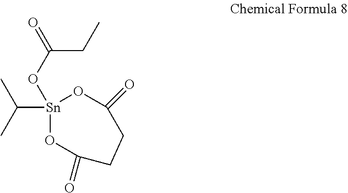
- a compound represented by Chemical Formula 8 was obtained with a yield of 79% according to substantially the same method as Synthesis Example 4 except that succinic acid was used instead of the malonic acid.
- PhSnCl 3 (3 g, 9.9 mmol) and Et 3 N (2 g, 19.8 mmol) were dissolved in 20 ml of toluene, and malonic acid (1 g, 9.9 mmol) dissolved in 10 ml of acetonitrile was slowly added thereto in a dropwise fashion while the 50 ml 2-neck round-bottomed flask was in an ice bath.
- iPrSnPh 3 (3 g, 7.6 mmol) and malonic acid (1.2 g, 11.4 mmol) were dissolved in 20 ml of acetonitrile and then, heated and refluxed for 24 hours. Subsequently, the solvent (acetonitrile) was completely removed through vacuum distillation to obtain a compound represented by Chemical Formula 10 with a yield of 83%.
- a compound represented by Chemical Formula 11 was obtained with a yield of 82% according to substantially the same method as Synthesis Example 7 except that succinic acid was used instead of the malonic acid.
- Neopentyltin trichloride (10 g, 18.7 mmol) was dissolved in anhydrous pentane and then, cooled down to 0° C. Subsequently, diethylamine (7.4 g, 101.3 mmol) was slowly added thereto in a dropwise fashion, and then, ethanol (6.1 g, 101.3 mmol) was added thereto and then, stirred at room temperature for 1 hour. When a reaction was complete, the solution was filtered, concentrated, and vacuum-dried to obtain a compound represented by Chemical Formula 12 with a yield of 60%.
- the compound represented by Chemical Formula 4 synthesized in Synthesis Example 1 and the compound represented by Chemical Formula 7 synthesized in Synthesis Example 4 were mixed to the same weight (same weight ratio) and then, dissolved in xylene at a concentration of 2.5 wt % and filtered with a 0.1 ⁇ m PTFE syringe filter to prepare a semiconductor photoresist composition according to Example 9.
- the compound represented by Chemical Formula 7 synthesized in Synthesis Example 4 and the compound represented by Chemical Formula 10 synthesized in Synthesis Example 7 were mixed to the same weight (same weight ratio) and then, dissolved in xylene at a concentration of 2.5 wt % and filtered with a 0.1 ⁇ m PTFE syringe filter to prepare a semiconductor photoresist composition according to Example 10.
- a circular silicon wafer having a diameter of 4 inches and a native-oxide surface was used as a substrate for depositing a thin film, and the substrate was pretreated under a UV ozone cleaning system for 10 minutes. Subsequently, the photoresist compositions for a semiconductor according to Examples 1 to 11 were respectively spin-coated on the pretreated substrate at 1,500 rpm for 30 seconds, baked (baked after applied, post-apply baked, PAB) on a hot plate at 100° C. for 120 seconds to form thin films.
- the thicknesses of the films were measured through Ellipsometry, and were each determined to be about 25 nm.
- a compound represented by Chemical Formula 12 synthesized in Comparative Synthesis Example 1 was dissolved in xylene at a concentration of 2 wt % and then, filtered with a 0.1 ⁇ m PTFE syringe filter to obtain a compound according to Comparative Example 1.
- the semiconductor photoresist composition according to Comparative Example 1 was coated on a substrate through substantially the same process as the examples to form a thin film.
- the thicknesses of the film was measured through Ellipsometry, and determined to be about 20 nm.
- a linear array of 50 disk pads having a diameter of 500 ⁇ m was irradiated into a wafer coated with each of the semiconductor photoresist composition resists according to Example 1 to Example 11 and Comparative Example 1 by using EUV ray (Lawrence Berkeley National Laboratory Micro Exposure Tool, MET). Exposure times of the pads were adjusted to apply an increased EUV dose to each pad.
- a residual resist thickness of the exposed pads was measured by using an Ellipsometer.
- the residual thickness with respect to each exposure dose was measured and graphed as a function of exposure doses, and D g (does to gel, energy when 95% of an initial thickness remains) depending on types of resists are shown in Table 1.
- the semiconductor photoresist compositions according to Examples 1 to 11 and Comparative Example 1 were allowed to stand at room temperature (in a range of 0° C. to 30° C.) a time and examined with naked eyes (unassisted eyes) to evaluate a degree of precipitation and then, classified into two groups depending on the following storage standards.
- ⁇ : can be stored for more than 1 month
- X can be stored for less than 2 weeks
- the semiconductor photoresist compositions of Examples 1 to 11 exhibited excellent storage stability compared with that of Comparative Example 1, and in addition, patterns formed of the semiconductor photoresist compositions of Examples 1 to 11 exhibited much more excellent sensitivity compared with that formed of the semiconductor photoresist composition of Comparative Example 1.
Landscapes
- Chemical & Material Sciences (AREA)
- Organic Chemistry (AREA)
- Physics & Mathematics (AREA)
- General Physics & Mathematics (AREA)
- Materials For Photolithography (AREA)
- Exposure And Positioning Against Photoresist Photosensitive Materials (AREA)
- Organic Low-Molecular-Weight Compounds And Preparation Thereof (AREA)
- Photosensitive Polymer And Photoresist Processing (AREA)
Abstract
Description


| TABLE 1 | ||
| Storage | Dg | |
| stability | (mJ/cm2) | |
| Example 1 | ◯ | 14.96 | |
| Example 2 | ◯ | 10.94 | |
| Example 3 | ◯ | 15.53 | |
| Example 4 | ◯ | 14.96 | |
| Example 5 | ◯ | 15.53 | |
| Example 6 | ◯ | 20.46 | |
| Example 7 | ◯ | 14.96 | |
| Example 8 | ◯ | 15.53 | |
| Example 9 | ◯ | 14.96 | |
| Example 10 | ◯ | 14.96 | |
| Example 11 | ◯ | 14.96 | |
| Comparative Example 1 | X | 25.21 | |
| Description of Symbols |
| 100: substrate | 102: thin layer | |
| 104: photoresist underlayer | 106: photoresist layer | |
| 106a: |
106b: exposed region | |
| 108: photoresist pattern | 112: organic layer pattern | |
| 114: thin layer pattern | ||
Claims (14)

Applications Claiming Priority (2)
| Application Number | Priority Date | Filing Date | Title |
|---|---|---|---|
| KR10-2019-0127958 | 2019-10-15 | ||
| KR1020190127958A KR102446362B1 (en) | 2019-10-15 | 2019-10-15 | Semiconductor resist composition, and method of forming patterns using the composition |
Publications (2)
| Publication Number | Publication Date |
|---|---|
| US20210109442A1 US20210109442A1 (en) | 2021-04-15 |
| US11415885B2 true US11415885B2 (en) | 2022-08-16 |
Family
ID=75383002
Family Applications (1)
| Application Number | Title | Priority Date | Filing Date |
|---|---|---|---|
| US17/036,693 Active US11415885B2 (en) | 2019-10-15 | 2020-09-29 | Semiconductor photoresist composition, and method of forming patterns using the composition |
Country Status (5)
| Country | Link |
|---|---|
| US (1) | US11415885B2 (en) |
| JP (1) | JP7028940B2 (en) |
| KR (1) | KR102446362B1 (en) |
| CN (1) | CN112666794B (en) |
| TW (1) | TWI745113B (en) |
Families Citing this family (12)
| Publication number | Priority date | Publication date | Assignee | Title |
|---|---|---|---|---|
| JP7456023B2 (en) * | 2020-07-02 | 2024-03-26 | アプライド マテリアルズ インコーポレイテッド | Selective deposition of carbon onto photoresist layers for lithography applications |
| US11906901B2 (en) * | 2021-06-07 | 2024-02-20 | International Business Machines Corporation | Alternating copolymer chain scission photoresists |
| US20230037563A1 (en) * | 2021-07-08 | 2023-02-09 | Samsung Sdi Co., Ltd. | Metal containing photoresist developer composition, and method of forming patterns including developing step using the same |
| KR102876476B1 (en) * | 2022-07-12 | 2025-10-23 | 삼성에스디아이 주식회사 | Semiconductor photoresist composition and method of forming patterns using the composition |
| KR102897992B1 (en) | 2022-11-16 | 2025-12-08 | 삼성에스디아이 주식회사 | Semiconductor photoresist composition and method of forming patterns using the composition |
| KR20240101079A (en) * | 2022-12-23 | 2024-07-02 | 삼성전자주식회사 | Composition for semiconductor photoresist and method of forming a pattern using the same |
| KR102795123B1 (en) * | 2023-01-04 | 2025-04-10 | 삼성에스디아이 주식회사 | Semiconductor photoresist composition and method of forming patterns using the composition |
| JP2025032887A (en) | 2023-08-28 | 2025-03-12 | 信越化学工業株式会社 | Compound for forming metal-containing film, composition for forming metal-containing film, and method for forming pattern |
| JP2025032875A (en) * | 2023-08-28 | 2025-03-12 | 信越化学工業株式会社 | Compound for forming metal-containing film, composition for forming metal-containing film, and method for forming pattern |
| US20250076755A1 (en) * | 2023-08-31 | 2025-03-06 | Feng Lu | Organotin photoresist composition for photolithography patterning |
| JP2025099887A (en) | 2023-12-22 | 2025-07-03 | 信越化学工業株式会社 | Compound for forming metal-containing film, composition for forming metal-containing film, and patterning process |
| JP2025099570A (en) | 2023-12-22 | 2025-07-03 | 信越化学工業株式会社 | Compound for forming metal-containing film, composition for forming metal-containing film, and patterning process |
Citations (37)
| Publication number | Priority date | Publication date | Assignee | Title |
|---|---|---|---|---|
| US3479380A (en) | 1967-03-03 | 1969-11-18 | Tenneco Chem | Dialkyltin,1,4-endoalkylene-2,3-dihydrophthalates and -1,2,3,6 - tetrahydrophthalates |
| JPS5072948A (en) | 1973-10-29 | 1975-06-16 | ||
| US5061599A (en) | 1986-06-11 | 1991-10-29 | Hitachi, Ltd. | Radiation sensitive materials |
| US5286599A (en) | 1991-09-26 | 1994-02-15 | International Business Machines Corporation | Base developable negative photoresist composition and use thereof |
| US6103448A (en) | 1997-10-08 | 2000-08-15 | Korea Advanced Institute Of Science And Technology | Organometal-containing acrylate or methacrylate derivatives and photoresists containing the polymers thereof |
| KR20020005063A (en) | 2000-06-30 | 2002-01-17 | 윤덕용 | Organometal-containing norbornene monomer, photoresist containing its polymer, manufacturing methods thereof, and method of forming photoresist patterns |
| JP2002072401A (en) | 2000-08-25 | 2002-03-12 | Fuji Photo Film Co Ltd | Silver halide photographic sensitive material |
| US20020072009A1 (en) | 2000-12-13 | 2002-06-13 | Kim Hyun-Woo | Photosensitive polymer containing Si, Ge or Sn and resist composition comprising the same |
| JP2003506532A (en) | 1999-08-04 | 2003-02-18 | コーツ ブラザーズ ピーエルシー | Organosilicon compounds and their use as photoinitiators |
| US20030129740A1 (en) | 2002-01-07 | 2003-07-10 | Kang-Il Seo | Method of preparing substrate having functional group pattern for immobilizing physiological material |
| US6689540B2 (en) | 2000-06-15 | 2004-02-10 | International Business Machines Corporation | Polymers and use thereof |
| KR20040078584A (en) | 2003-03-03 | 2004-09-10 | 롬 앤드 하스 일렉트로닉 머트어리얼즈, 엘.엘.씨. | Si-Polymers and photoresists comprising same |
| US20060128919A1 (en) * | 2002-11-01 | 2006-06-15 | Toshihiko Okamoto | Curable composition and methods for improving recovery properties and creep properties |
| EP1177182B1 (en) | 1999-05-10 | 2006-11-29 | Ciba SC Holding AG | Novel photoinitiators and their applications |
| JP3904518B2 (en) | 2001-04-09 | 2007-04-11 | 積水化学工業株式会社 | Photoreactive composition |
| US7294449B1 (en) | 2003-12-31 | 2007-11-13 | Kovio, Inc. | Radiation patternable functional materials, methods of their use, and structures formed therefrom |
| JP2008007610A (en) | 2006-06-28 | 2008-01-17 | Nippon Soda Co Ltd | Organic/inorganic composite and its production process |
| US7323275B2 (en) | 2001-02-09 | 2008-01-29 | Dai Nippon Printing Co., Ltd | Photosensitive composition for volume hologram recording and photosensitive medium for volume hologram recording |
| US20110045406A1 (en) | 2006-11-01 | 2011-02-24 | State of Oregon acting by and through the State Board of Higher Education on behalf of Oregon | Solution processed thin films and laminates, devices comprising such thin films and laminates, and method for their use and manufacture |
| US20110184139A1 (en) | 2008-08-07 | 2011-07-28 | Mangala Malik | Metal compositions and methods of making same |
| US20120208127A1 (en) | 2011-02-15 | 2012-08-16 | Shin-Etsu Chemical Co., Ltd. | Resist composition and patterning process |
| JP5028887B2 (en) | 2006-07-04 | 2012-09-19 | ダイキン工業株式会社 | Fluorine-based photosensitive composition |
| US20130005150A1 (en) | 2011-06-28 | 2013-01-03 | Shin-Etsu Chemical Co., Ltd. | Composition for forming resist underlayer film and patterning process using the same |
| US20130224652A1 (en) | 2012-02-27 | 2013-08-29 | International Business Machines Corporation | Metal peroxo compounds with organic co-ligands for electron beam, deep uv and extreme uv photoresist applications |
| WO2014098076A1 (en) | 2012-12-19 | 2014-06-26 | 日産化学工業株式会社 | Composition for forming silicon-containing resist underlayer film having cyclic diester group |
| US9261784B2 (en) | 2011-07-08 | 2016-02-16 | Asml Netherlands B.V. | Lithographic patterning process and resists to use therein |
| US20160116839A1 (en) | 2014-10-23 | 2016-04-28 | Inpria Corporation | Organometallic solution based high resolution patterning compositions and corresponding methods |
| US9372402B2 (en) | 2013-09-13 | 2016-06-21 | The Research Foundation For The State University Of New York | Molecular organometallic resists for EUV |
| US20160230019A1 (en) | 2015-02-11 | 2016-08-11 | Az Electronic Materials (Luxembourg) S.A.R.L | Metal hardmask composition and processes for forming fine patterns on semiconductor substrates |
| WO2016140057A1 (en) | 2015-03-05 | 2016-09-09 | Jsr株式会社 | Radiation-sensitive composition and pattern formation method |
| US20170052449A1 (en) | 2015-08-20 | 2017-02-23 | Osaka University | Chemically amplified resist material, pattern-forming method, compound, and production method of compound |
| US20170102612A1 (en) | 2015-10-13 | 2017-04-13 | Inpria Corporation | Organotin oxide hydroxide patterning compositions, precursors, and patterning |
| US20170146909A1 (en) | 2015-11-20 | 2017-05-25 | Lam Research Corporation | Euv photopatterning of vapor-deposited metal oxide-containing hardmasks |
| US20170269476A1 (en) | 2014-12-02 | 2017-09-21 | Jsr Corporation | Photoresist composition, production method of photoresist composition, and resist pattern-forming method |
| JP2017207532A (en) | 2016-05-16 | 2017-11-24 | 東洋合成工業株式会社 | Resist composition and method for producing device using the same |
| WO2018123388A1 (en) | 2016-12-28 | 2018-07-05 | Jsr株式会社 | Radiation-sensitive composition, pattern formation method, and metal-containing resin and method for manufacturing same |
| US20200041896A1 (en) * | 2018-07-31 | 2020-02-06 | Samsung Sdi Co., Ltd. | Semiconductor resist composition, and method of forming patterns using the composition |
Family Cites Families (9)
| Publication number | Priority date | Publication date | Assignee | Title |
|---|---|---|---|---|
| JPS5936943B2 (en) * | 1977-01-12 | 1984-09-06 | 三共有機合成株式会社 | Stabilized halogen-containing polymer composition |
| JPH0354245A (en) * | 1989-07-21 | 1991-03-08 | Nitto Kasei Co Ltd | Stabilized chlorinated vinyl chloride resin composition |
| JP4597037B2 (en) * | 2004-11-08 | 2010-12-15 | 日東化成株式会社 | Chlorine-containing resin composition |
| JP2009301020A (en) * | 2008-05-16 | 2009-12-24 | Sumitomo Chemical Co Ltd | Chemically amplified positive resist composition |
| KR101400182B1 (en) * | 2009-12-31 | 2014-05-27 | 제일모직 주식회사 | Photoresist underlayer composition and method of manufacturing semiconductor device by using the same |
| CN102503972B (en) * | 2011-09-28 | 2015-06-17 | 衢州建华东旭助剂有限公司 | Methyltin maleate and preparation method thereof |
| CN106279263B (en) * | 2016-08-31 | 2018-06-05 | 湖北犇星化工有限责任公司 | The preparation method of Methyltin maleate |
| KR20190082279A (en) * | 2016-11-07 | 2019-07-09 | 도요 고세이 고교 가부시키가이샤 | Metal-containing onium salt compounds, photo-degradable bases and resist compositions, and methods of manufacturing devices using the resist compositions |
| CN110305440B (en) * | 2019-06-17 | 2021-07-13 | 金发科技股份有限公司 | Environment-friendly flame-retardant ABS (acrylonitrile-butadiene-styrene) composite material and preparation method thereof |
-
2019
- 2019-10-15 KR KR1020190127958A patent/KR102446362B1/en active Active
-
2020
- 2020-09-29 US US17/036,693 patent/US11415885B2/en active Active
- 2020-10-07 TW TW109134748A patent/TWI745113B/en active
- 2020-10-12 JP JP2020171971A patent/JP7028940B2/en active Active
- 2020-10-14 CN CN202011093850.2A patent/CN112666794B/en active Active
Patent Citations (60)
| Publication number | Priority date | Publication date | Assignee | Title |
|---|---|---|---|---|
| US3479380A (en) | 1967-03-03 | 1969-11-18 | Tenneco Chem | Dialkyltin,1,4-endoalkylene-2,3-dihydrophthalates and -1,2,3,6 - tetrahydrophthalates |
| JPS5072948A (en) | 1973-10-29 | 1975-06-16 | ||
| US5061599A (en) | 1986-06-11 | 1991-10-29 | Hitachi, Ltd. | Radiation sensitive materials |
| US5286599A (en) | 1991-09-26 | 1994-02-15 | International Business Machines Corporation | Base developable negative photoresist composition and use thereof |
| JP2683536B2 (en) | 1991-09-26 | 1997-12-03 | インターナショナル・ビジネス・マシーンズ・コーポレイション | Base developable negative photoresist composition and image forming method using the same |
| US6103448A (en) | 1997-10-08 | 2000-08-15 | Korea Advanced Institute Of Science And Technology | Organometal-containing acrylate or methacrylate derivatives and photoresists containing the polymers thereof |
| KR100269513B1 (en) | 1997-10-08 | 2000-10-16 | 윤덕용 | New acrylate or methacrylate derivatives and photoresist containing its polymer |
| EP1177182B1 (en) | 1999-05-10 | 2006-11-29 | Ciba SC Holding AG | Novel photoinitiators and their applications |
| US6849668B1 (en) | 1999-08-04 | 2005-02-01 | Sun Chemical Corporation | Organo-silicon compounds and their use as photoinitiators |
| JP2003506532A (en) | 1999-08-04 | 2003-02-18 | コーツ ブラザーズ ピーエルシー | Organosilicon compounds and their use as photoinitiators |
| US6689540B2 (en) | 2000-06-15 | 2004-02-10 | International Business Machines Corporation | Polymers and use thereof |
| US6607867B1 (en) | 2000-06-30 | 2003-08-19 | Korea Advanced Institute Of Science And Technology | Organometal-containing norbornene monomer, photoresist containing its polymer, manufacturing method thereof, and method of forming photoresist patterns |
| KR100398312B1 (en) | 2000-06-30 | 2003-09-19 | 한국과학기술원 | Organometal-containing norbornene monomer, photoresist containing its polymer, manufacturing methods thereof, and method of forming photoresist patterns |
| KR20020005063A (en) | 2000-06-30 | 2002-01-17 | 윤덕용 | Organometal-containing norbornene monomer, photoresist containing its polymer, manufacturing methods thereof, and method of forming photoresist patterns |
| JP2002072401A (en) | 2000-08-25 | 2002-03-12 | Fuji Photo Film Co Ltd | Silver halide photographic sensitive material |
| JP3990146B2 (en) | 2000-12-13 | 2007-10-10 | 三星電子株式会社 | Photosensitive polymer containing silicon and resist composition containing the same |
| US20020072009A1 (en) | 2000-12-13 | 2002-06-13 | Kim Hyun-Woo | Photosensitive polymer containing Si, Ge or Sn and resist composition comprising the same |
| US7323275B2 (en) | 2001-02-09 | 2008-01-29 | Dai Nippon Printing Co., Ltd | Photosensitive composition for volume hologram recording and photosensitive medium for volume hologram recording |
| US7312013B2 (en) | 2001-04-09 | 2007-12-25 | Sekisui Chemical Co., Ltd. | Photoreactive composition |
| JP3904518B2 (en) | 2001-04-09 | 2007-04-11 | 積水化学工業株式会社 | Photoreactive composition |
| US20030129740A1 (en) | 2002-01-07 | 2003-07-10 | Kang-Il Seo | Method of preparing substrate having functional group pattern for immobilizing physiological material |
| US20060128919A1 (en) * | 2002-11-01 | 2006-06-15 | Toshihiko Okamoto | Curable composition and methods for improving recovery properties and creep properties |
| US20040248032A1 (en) | 2003-03-03 | 2004-12-09 | Anthony Zampini | Polymers and photoresists comprising same |
| KR20040078584A (en) | 2003-03-03 | 2004-09-10 | 롬 앤드 하스 일렉트로닉 머트어리얼즈, 엘.엘.씨. | Si-Polymers and photoresists comprising same |
| JP5178858B2 (en) | 2003-03-03 | 2013-04-10 | ローム・アンド・ハース・エレクトロニック・マテリアルズ,エル.エル.シー. | Polymer and photoresist containing the same |
| US7294449B1 (en) | 2003-12-31 | 2007-11-13 | Kovio, Inc. | Radiation patternable functional materials, methods of their use, and structures formed therefrom |
| JP2008007610A (en) | 2006-06-28 | 2008-01-17 | Nippon Soda Co Ltd | Organic/inorganic composite and its production process |
| JP5028887B2 (en) | 2006-07-04 | 2012-09-19 | ダイキン工業株式会社 | Fluorine-based photosensitive composition |
| US20110045406A1 (en) | 2006-11-01 | 2011-02-24 | State of Oregon acting by and through the State Board of Higher Education on behalf of Oregon | Solution processed thin films and laminates, devices comprising such thin films and laminates, and method for their use and manufacture |
| US20110184139A1 (en) | 2008-08-07 | 2011-07-28 | Mangala Malik | Metal compositions and methods of making same |
| JP6004649B2 (en) | 2008-08-07 | 2016-10-12 | プライオグ リミテッド ライアビリティ カンパニーPryog,Llc | Metal composition and process for producing the same |
| US9164383B2 (en) | 2011-02-15 | 2015-10-20 | Shin-Etsu Chemical Co., Ltd. | Resist composition and patterning process |
| JP5708521B2 (en) | 2011-02-15 | 2015-04-30 | 信越化学工業株式会社 | Resist material and pattern forming method using the same |
| US20120208127A1 (en) | 2011-02-15 | 2012-08-16 | Shin-Etsu Chemical Co., Ltd. | Resist composition and patterning process |
| JP5650086B2 (en) | 2011-06-28 | 2015-01-07 | 信越化学工業株式会社 | Resist underlayer film forming composition and pattern forming method |
| US20130005150A1 (en) | 2011-06-28 | 2013-01-03 | Shin-Etsu Chemical Co., Ltd. | Composition for forming resist underlayer film and patterning process using the same |
| US9261784B2 (en) | 2011-07-08 | 2016-02-16 | Asml Netherlands B.V. | Lithographic patterning process and resists to use therein |
| US20130224652A1 (en) | 2012-02-27 | 2013-08-29 | International Business Machines Corporation | Metal peroxo compounds with organic co-ligands for electron beam, deep uv and extreme uv photoresist applications |
| KR20140121826A (en) | 2012-02-27 | 2014-10-16 | 인터내셔널 비지네스 머신즈 코포레이션 | Metal peroxo compounds with organic co-ligands for electron beam, deep uv and extreme uv photoresist applications |
| WO2014098076A1 (en) | 2012-12-19 | 2014-06-26 | 日産化学工業株式会社 | Composition for forming silicon-containing resist underlayer film having cyclic diester group |
| US9372402B2 (en) | 2013-09-13 | 2016-06-21 | The Research Foundation For The State University Of New York | Molecular organometallic resists for EUV |
| JP2018502173A (en) | 2014-10-23 | 2018-01-25 | インプリア・コーポレイションInpria Corporation | High resolution patterning compositions based on organometallic solutions and corresponding methods |
| US20210048745A1 (en) | 2014-10-23 | 2021-02-18 | Inpria Corporation | Organometallic solution based high resolution patterning compositions and corresponding methods |
| US20160116839A1 (en) | 2014-10-23 | 2016-04-28 | Inpria Corporation | Organometallic solution based high resolution patterning compositions and corresponding methods |
| US20170269476A1 (en) | 2014-12-02 | 2017-09-21 | Jsr Corporation | Photoresist composition, production method of photoresist composition, and resist pattern-forming method |
| KR20170116134A (en) | 2015-02-11 | 2017-10-18 | 에이제트 일렉트로닉 머티어리얼스 (룩셈부르크) 에스.에이.알.엘. | METAL HARD MASK COMPOSITION AND METHOD FOR FORMING A MICROPARATIC PATTERN |
| US20160230019A1 (en) | 2015-02-11 | 2016-08-11 | Az Electronic Materials (Luxembourg) S.A.R.L | Metal hardmask composition and processes for forming fine patterns on semiconductor substrates |
| WO2016140057A1 (en) | 2015-03-05 | 2016-09-09 | Jsr株式会社 | Radiation-sensitive composition and pattern formation method |
| US20170052449A1 (en) | 2015-08-20 | 2017-02-23 | Osaka University | Chemically amplified resist material, pattern-forming method, compound, and production method of compound |
| KR20170022945A (en) | 2015-08-20 | 2017-03-02 | 고꾸리쯔 다이가꾸 호우징 오사까 다이가꾸 | Chemically amplified resist material, pattern-forming method, compound, and production method of compound |
| US20170102612A1 (en) | 2015-10-13 | 2017-04-13 | Inpria Corporation | Organotin oxide hydroxide patterning compositions, precursors, and patterning |
| KR20180054917A (en) | 2015-10-13 | 2018-05-24 | 인프리아 코포레이션 | Organotin oxide hydroxide patterning composition, precursor and patterning |
| JP2019500490A (en) | 2015-10-13 | 2019-01-10 | インプリア・コーポレイションInpria Corporation | Organotin oxide hydroxide patterning compositions, precursors and patterning |
| KR20170066225A (en) | 2015-11-20 | 2017-06-14 | 램 리써치 코포레이션 | Euv photopatterning of vapor-deposited metal oxide-containing hardmasks |
| US20170146909A1 (en) | 2015-11-20 | 2017-05-25 | Lam Research Corporation | Euv photopatterning of vapor-deposited metal oxide-containing hardmasks |
| JP2017207532A (en) | 2016-05-16 | 2017-11-24 | 東洋合成工業株式会社 | Resist composition and method for producing device using the same |
| WO2018123388A1 (en) | 2016-12-28 | 2018-07-05 | Jsr株式会社 | Radiation-sensitive composition, pattern formation method, and metal-containing resin and method for manufacturing same |
| TW201831570A (en) | 2016-12-28 | 2018-09-01 | 日商Jsr 股份有限公司 | Radiation-sensitive composition, pattern formation method, and metal-containing resin and method for manufacturing same |
| US20190310552A1 (en) | 2016-12-28 | 2019-10-10 | Jsr Corporation | Radiation-sensitive composition, pattern-forming method, and metal-containing resin and production method thereof |
| US20200041896A1 (en) * | 2018-07-31 | 2020-02-06 | Samsung Sdi Co., Ltd. | Semiconductor resist composition, and method of forming patterns using the composition |
Non-Patent Citations (9)
| Title |
|---|
| Anderson, Christopher et al.; "The SEMATECH Berkeley MET: extending EUV learning down to 16nm half pitch"; Proc. Of SPIE; vol. 7969; 2011; 7pp. |
| Japanese Office Action dated Oct. 5, 2021, issued in corresponding Japanese Patent Application No. 2020-171971 (2 pages). |
| Korean Office Action dated Jan. 7, 2021, of the corresponding Korean Patent Application No. 10-2018-0089413 (6 pages). |
| Notice of Allowability (including Search Report dated Jul. 9, 2021) for Corresponding Taiwan Patent Application No. 109134748, dated Jul. 12, 2021 (3 pages). |
| Okamoto, Hiroshi et al.; "Peroxypolytungstic acids: A new inorganic resist material"; Applied Physics Letters; 49; 298; 1986; 4pp. |
| Stowers, Jason K. et al.; "Directly patterned inorganic hardmask for EUV lithography"; Proc. Of SPIE; vol. 7969; 2011; 12pp. |
| U.S. Notice of Allowance from U.S. Appl. No. 16/211,114, dated Apr. 21, 2021, 7 pages. |
| U.S. Office Action from U.S. Appl. No. 16/211,114, dated Nov. 16, 2020, 8 pages. |
| U.S. Restriction Requirement from U.S. Appl. No. 16/211,114, dated Jun. 12, 2020, 7 pages. |
Also Published As
| Publication number | Publication date |
|---|---|
| KR102446362B1 (en) | 2022-09-21 |
| JP7028940B2 (en) | 2022-03-02 |
| KR20210044592A (en) | 2021-04-23 |
| CN112666794A (en) | 2021-04-16 |
| TWI745113B (en) | 2021-11-01 |
| US20210109442A1 (en) | 2021-04-15 |
| TW202116788A (en) | 2021-05-01 |
| JP2021063985A (en) | 2021-04-22 |
| CN112666794B (en) | 2024-12-17 |
Similar Documents
| Publication | Publication Date | Title |
|---|---|---|
| US11415885B2 (en) | Semiconductor photoresist composition, and method of forming patterns using the composition | |
| US11609494B2 (en) | Semiconductor photoresist composition and method of forming patterns using the composition | |
| US11789362B2 (en) | Semiconductor resist composition, and method of forming patterns using the composition | |
| US12306534B2 (en) | Semiconductor photoresist composition and method of forming patterns using the composition | |
| US11789361B2 (en) | Semiconductor resist composition, and method of forming patterns using the composition | |
| US20210311387A1 (en) | Semiconductor photoresist composition and method of forming patterns using the composition | |
| US11073761B2 (en) | Semiconductor resist composition, and method of forming patterns using the composition | |
| TW202041513A (en) | Semiconductor photoresist composition and method of forming patterns using the composition | |
| US12538761B2 (en) | Composition for semiconductor photoresist, and pattern formation method using same | |
| TWI867534B (en) | Semiconductor photoresist composition and method of forming patterns using the composition | |
| KR102904140B1 (en) | Semiconductor photoresist composition and method of forming patterns using the composition | |
| KR102446361B1 (en) | Semiconductor resist composition, and method of forming patterns using the composition | |
| KR20250172918A (en) | Semiconductor photoresist composition and method of forming patterns using the composition | |
| KR102854753B1 (en) | Semiconductor photoresist composition and method of forming patterns using the composition | |
| US20250216777A1 (en) | Semiconductor photoresist composition and method of forming patterns using the composition | |
| US20250102907A1 (en) | Semiconductor photoresist composition and method of forming patterns using the composition | |
| KR102848413B1 (en) | Semiconductor photoresist composition and method of forming patterns using the composition | |
| US20260036902A1 (en) | Semiconductor photoresist compositions and methods of forming patterns using the compositions | |
| KR20250145344A (en) | Semiconductor photoresist composition and method of forming patterns using the composition | |
| KR20250160732A (en) | Semiconductor photoresist composition and method of forming patterns using the composition | |
| TW202506697A (en) | Method of forming patterns | |
| KR20230023410A (en) | Semiconductor photoresist composition and method of forming patterns using the composition |
Legal Events
| Date | Code | Title | Description |
|---|---|---|---|
| AS | Assignment |
Owner name: SAMSUNG SDI CO., LTD., KOREA, REPUBLIC OF Free format text: ASSIGNMENT OF ASSIGNORS INTEREST;ASSIGNORS:MOON, KYUNGSOO;KANG, EUNMI;KIM, JAEHYUN;AND OTHERS;REEL/FRAME:053919/0524 Effective date: 20200929 |
|
| FEPP | Fee payment procedure |
Free format text: ENTITY STATUS SET TO UNDISCOUNTED (ORIGINAL EVENT CODE: BIG.); ENTITY STATUS OF PATENT OWNER: LARGE ENTITY |
|
| STPP | Information on status: patent application and granting procedure in general |
Free format text: RESPONSE TO NON-FINAL OFFICE ACTION ENTERED AND FORWARDED TO EXAMINER |
|
| STPP | Information on status: patent application and granting procedure in general |
Free format text: NON FINAL ACTION MAILED |
|
| STPP | Information on status: patent application and granting procedure in general |
Free format text: RESPONSE TO NON-FINAL OFFICE ACTION ENTERED AND FORWARDED TO EXAMINER |
|
| STPP | Information on status: patent application and granting procedure in general |
Free format text: AWAITING TC RESP., ISSUE FEE NOT PAID |
|
| STPP | Information on status: patent application and granting procedure in general |
Free format text: NOTICE OF ALLOWANCE MAILED -- APPLICATION RECEIVED IN OFFICE OF PUBLICATIONS |
|
| STPP | Information on status: patent application and granting procedure in general |
Free format text: NOTICE OF ALLOWANCE MAILED -- APPLICATION RECEIVED IN OFFICE OF PUBLICATIONS |
|
| STPP | Information on status: patent application and granting procedure in general |
Free format text: DOCKETED NEW CASE - READY FOR EXAMINATION |
|
| STPP | Information on status: patent application and granting procedure in general |
Free format text: NOTICE OF ALLOWANCE MAILED -- APPLICATION RECEIVED IN OFFICE OF PUBLICATIONS |
|
| STPP | Information on status: patent application and granting procedure in general |
Free format text: PUBLICATIONS -- ISSUE FEE PAYMENT VERIFIED |
|
| STCF | Information on status: patent grant |
Free format text: PATENTED CASE |
|
| MAFP | Maintenance fee payment |
Free format text: PAYMENT OF MAINTENANCE FEE, 4TH YEAR, LARGE ENTITY (ORIGINAL EVENT CODE: M1551); ENTITY STATUS OF PATENT OWNER: LARGE ENTITY Year of fee payment: 4 |