US11401609B2 - Film forming method and film forming system - Google Patents
Film forming method and film forming system Download PDFInfo
- Publication number
- US11401609B2 US11401609B2 US16/553,602 US201916553602A US11401609B2 US 11401609 B2 US11401609 B2 US 11401609B2 US 201916553602 A US201916553602 A US 201916553602A US 11401609 B2 US11401609 B2 US 11401609B2
- Authority
- US
- United States
- Prior art keywords
- film
- gas
- film forming
- gas supply
- processing container
- Prior art date
- Legal status (The legal status is an assumption and is not a legal conclusion. Google has not performed a legal analysis and makes no representation as to the accuracy of the status listed.)
- Active, expires
Links
Images


Classifications
-
- H—ELECTRICITY
- H10—SEMICONDUCTOR DEVICES; ELECTRIC SOLID-STATE DEVICES NOT OTHERWISE PROVIDED FOR
- H10W—GENERIC PACKAGES, INTERCONNECTIONS, CONNECTORS OR OTHER CONSTRUCTIONAL DETAILS OF DEVICES COVERED BY CLASS H10
- H10W20/00—Interconnections in chips, wafers or substrates
- H10W20/01—Manufacture or treatment
- H10W20/071—Manufacture or treatment of dielectric parts thereof
- H10W20/074—Manufacture or treatment of dielectric parts thereof of dielectric parts comprising thin functional dielectric layers, e.g. dielectric etch-stop, barrier, capping or liner layers
- H10W20/076—Manufacture or treatment of dielectric parts thereof of dielectric parts comprising thin functional dielectric layers, e.g. dielectric etch-stop, barrier, capping or liner layers in via holes or trenches
-
- H—ELECTRICITY
- H10—SEMICONDUCTOR DEVICES; ELECTRIC SOLID-STATE DEVICES NOT OTHERWISE PROVIDED FOR
- H10D—INORGANIC ELECTRIC SEMICONDUCTOR DEVICES
- H10D64/00—Electrodes of devices having potential barriers
- H10D64/01—Manufacture or treatment
- H10D64/013—Manufacture or treatment of electrodes having a conductor capacitively coupled to a semiconductor by an insulator
- H10D64/01302—Manufacture or treatment of electrodes having a conductor capacitively coupled to a semiconductor by an insulator the insulator being formed after the semiconductor body, the semiconductor being silicon
- H10D64/01332—Making the insulator
- H10D64/01336—Making the insulator on single crystalline silicon, e.g. chemical oxidation using a liquid
- H10D64/01342—Making the insulator on single crystalline silicon, e.g. chemical oxidation using a liquid by deposition, e.g. evaporation, ALD or laser deposition
-
- C—CHEMISTRY; METALLURGY
- C23—COATING METALLIC MATERIAL; COATING MATERIAL WITH METALLIC MATERIAL; CHEMICAL SURFACE TREATMENT; DIFFUSION TREATMENT OF METALLIC MATERIAL; COATING BY VACUUM EVAPORATION, BY SPUTTERING, BY ION IMPLANTATION OR BY CHEMICAL VAPOUR DEPOSITION, IN GENERAL; INHIBITING CORROSION OF METALLIC MATERIAL OR INCRUSTATION IN GENERAL
- C23C—COATING METALLIC MATERIAL; COATING MATERIAL WITH METALLIC MATERIAL; SURFACE TREATMENT OF METALLIC MATERIAL BY DIFFUSION INTO THE SURFACE, BY CHEMICAL CONVERSION OR SUBSTITUTION; COATING BY VACUUM EVAPORATION, BY SPUTTERING, BY ION IMPLANTATION OR BY CHEMICAL VAPOUR DEPOSITION, IN GENERAL
- C23C16/00—Chemical coating by decomposition of gaseous compounds, without leaving reaction products of surface material in the coating, i.e. chemical vapour deposition [CVD] processes
- C23C16/44—Chemical coating by decomposition of gaseous compounds, without leaving reaction products of surface material in the coating, i.e. chemical vapour deposition [CVD] processes characterised by the method of coating
- C23C16/455—Chemical coating by decomposition of gaseous compounds, without leaving reaction products of surface material in the coating, i.e. chemical vapour deposition [CVD] processes characterised by the method of coating characterised by the method used for introducing gases into reaction chamber or for modifying gas flows in reaction chamber
- C23C16/45523—Pulsed gas flow or change of composition over time
- C23C16/45525—Atomic layer deposition [ALD]
- C23C16/45553—Atomic layer deposition [ALD] characterized by the use of precursors specially adapted for ALD
-
- C—CHEMISTRY; METALLURGY
- C23—COATING METALLIC MATERIAL; COATING MATERIAL WITH METALLIC MATERIAL; CHEMICAL SURFACE TREATMENT; DIFFUSION TREATMENT OF METALLIC MATERIAL; COATING BY VACUUM EVAPORATION, BY SPUTTERING, BY ION IMPLANTATION OR BY CHEMICAL VAPOUR DEPOSITION, IN GENERAL; INHIBITING CORROSION OF METALLIC MATERIAL OR INCRUSTATION IN GENERAL
- C23C—COATING METALLIC MATERIAL; COATING MATERIAL WITH METALLIC MATERIAL; SURFACE TREATMENT OF METALLIC MATERIAL BY DIFFUSION INTO THE SURFACE, BY CHEMICAL CONVERSION OR SUBSTITUTION; COATING BY VACUUM EVAPORATION, BY SPUTTERING, BY ION IMPLANTATION OR BY CHEMICAL VAPOUR DEPOSITION, IN GENERAL
- C23C16/00—Chemical coating by decomposition of gaseous compounds, without leaving reaction products of surface material in the coating, i.e. chemical vapour deposition [CVD] processes
- C23C16/02—Pretreatment of the material to be coated
- C23C16/0272—Deposition of sub-layers, e.g. to promote the adhesion of the main coating
- C23C16/0281—Deposition of sub-layers, e.g. to promote the adhesion of the main coating of metallic sub-layers
-
- C—CHEMISTRY; METALLURGY
- C23—COATING METALLIC MATERIAL; COATING MATERIAL WITH METALLIC MATERIAL; CHEMICAL SURFACE TREATMENT; DIFFUSION TREATMENT OF METALLIC MATERIAL; COATING BY VACUUM EVAPORATION, BY SPUTTERING, BY ION IMPLANTATION OR BY CHEMICAL VAPOUR DEPOSITION, IN GENERAL; INHIBITING CORROSION OF METALLIC MATERIAL OR INCRUSTATION IN GENERAL
- C23C—COATING METALLIC MATERIAL; COATING MATERIAL WITH METALLIC MATERIAL; SURFACE TREATMENT OF METALLIC MATERIAL BY DIFFUSION INTO THE SURFACE, BY CHEMICAL CONVERSION OR SUBSTITUTION; COATING BY VACUUM EVAPORATION, BY SPUTTERING, BY ION IMPLANTATION OR BY CHEMICAL VAPOUR DEPOSITION, IN GENERAL
- C23C16/00—Chemical coating by decomposition of gaseous compounds, without leaving reaction products of surface material in the coating, i.e. chemical vapour deposition [CVD] processes
- C23C16/06—Chemical coating by decomposition of gaseous compounds, without leaving reaction products of surface material in the coating, i.e. chemical vapour deposition [CVD] processes characterised by the deposition of metallic material
- C23C16/08—Chemical coating by decomposition of gaseous compounds, without leaving reaction products of surface material in the coating, i.e. chemical vapour deposition [CVD] processes characterised by the deposition of metallic material from metal halides
-
- C—CHEMISTRY; METALLURGY
- C23—COATING METALLIC MATERIAL; COATING MATERIAL WITH METALLIC MATERIAL; CHEMICAL SURFACE TREATMENT; DIFFUSION TREATMENT OF METALLIC MATERIAL; COATING BY VACUUM EVAPORATION, BY SPUTTERING, BY ION IMPLANTATION OR BY CHEMICAL VAPOUR DEPOSITION, IN GENERAL; INHIBITING CORROSION OF METALLIC MATERIAL OR INCRUSTATION IN GENERAL
- C23C—COATING METALLIC MATERIAL; COATING MATERIAL WITH METALLIC MATERIAL; SURFACE TREATMENT OF METALLIC MATERIAL BY DIFFUSION INTO THE SURFACE, BY CHEMICAL CONVERSION OR SUBSTITUTION; COATING BY VACUUM EVAPORATION, BY SPUTTERING, BY ION IMPLANTATION OR BY CHEMICAL VAPOUR DEPOSITION, IN GENERAL
- C23C16/00—Chemical coating by decomposition of gaseous compounds, without leaving reaction products of surface material in the coating, i.e. chemical vapour deposition [CVD] processes
- C23C16/22—Chemical coating by decomposition of gaseous compounds, without leaving reaction products of surface material in the coating, i.e. chemical vapour deposition [CVD] processes characterised by the deposition of inorganic material, other than metallic material
- C23C16/30—Deposition of compounds, mixtures or solid solutions, e.g. borides, carbides, nitrides
- C23C16/301—AIII BV compounds, where A is Al, Ga, In or Tl and B is N, P, As, Sb or Bi
- C23C16/303—Nitrides
-
- C—CHEMISTRY; METALLURGY
- C23—COATING METALLIC MATERIAL; COATING MATERIAL WITH METALLIC MATERIAL; CHEMICAL SURFACE TREATMENT; DIFFUSION TREATMENT OF METALLIC MATERIAL; COATING BY VACUUM EVAPORATION, BY SPUTTERING, BY ION IMPLANTATION OR BY CHEMICAL VAPOUR DEPOSITION, IN GENERAL; INHIBITING CORROSION OF METALLIC MATERIAL OR INCRUSTATION IN GENERAL
- C23C—COATING METALLIC MATERIAL; COATING MATERIAL WITH METALLIC MATERIAL; SURFACE TREATMENT OF METALLIC MATERIAL BY DIFFUSION INTO THE SURFACE, BY CHEMICAL CONVERSION OR SUBSTITUTION; COATING BY VACUUM EVAPORATION, BY SPUTTERING, BY ION IMPLANTATION OR BY CHEMICAL VAPOUR DEPOSITION, IN GENERAL
- C23C16/00—Chemical coating by decomposition of gaseous compounds, without leaving reaction products of surface material in the coating, i.e. chemical vapour deposition [CVD] processes
- C23C16/22—Chemical coating by decomposition of gaseous compounds, without leaving reaction products of surface material in the coating, i.e. chemical vapour deposition [CVD] processes characterised by the deposition of inorganic material, other than metallic material
- C23C16/30—Deposition of compounds, mixtures or solid solutions, e.g. borides, carbides, nitrides
- C23C16/34—Nitrides
-
- C—CHEMISTRY; METALLURGY
- C23—COATING METALLIC MATERIAL; COATING MATERIAL WITH METALLIC MATERIAL; CHEMICAL SURFACE TREATMENT; DIFFUSION TREATMENT OF METALLIC MATERIAL; COATING BY VACUUM EVAPORATION, BY SPUTTERING, BY ION IMPLANTATION OR BY CHEMICAL VAPOUR DEPOSITION, IN GENERAL; INHIBITING CORROSION OF METALLIC MATERIAL OR INCRUSTATION IN GENERAL
- C23C—COATING METALLIC MATERIAL; COATING MATERIAL WITH METALLIC MATERIAL; SURFACE TREATMENT OF METALLIC MATERIAL BY DIFFUSION INTO THE SURFACE, BY CHEMICAL CONVERSION OR SUBSTITUTION; COATING BY VACUUM EVAPORATION, BY SPUTTERING, BY ION IMPLANTATION OR BY CHEMICAL VAPOUR DEPOSITION, IN GENERAL
- C23C16/00—Chemical coating by decomposition of gaseous compounds, without leaving reaction products of surface material in the coating, i.e. chemical vapour deposition [CVD] processes
- C23C16/44—Chemical coating by decomposition of gaseous compounds, without leaving reaction products of surface material in the coating, i.e. chemical vapour deposition [CVD] processes characterised by the method of coating
-
- H01L21/28556—
-
- H—ELECTRICITY
- H10—SEMICONDUCTOR DEVICES; ELECTRIC SOLID-STATE DEVICES NOT OTHERWISE PROVIDED FOR
- H10P—GENERIC PROCESSES OR APPARATUS FOR THE MANUFACTURE OR TREATMENT OF DEVICES COVERED BY CLASS H10
- H10P14/00—Formation of materials, e.g. in the shape of layers or pillars
- H10P14/40—Formation of materials, e.g. in the shape of layers or pillars of conductive or resistive materials
- H10P14/42—Formation of materials, e.g. in the shape of layers or pillars of conductive or resistive materials using a gas or vapour
- H10P14/43—Chemical deposition, e.g. chemical vapour deposition [CVD]
- H10P14/432—Chemical deposition, e.g. chemical vapour deposition [CVD] using selective deposition
-
- H—ELECTRICITY
- H10—SEMICONDUCTOR DEVICES; ELECTRIC SOLID-STATE DEVICES NOT OTHERWISE PROVIDED FOR
- H10P—GENERIC PROCESSES OR APPARATUS FOR THE MANUFACTURE OR TREATMENT OF DEVICES COVERED BY CLASS H10
- H10P72/00—Handling or holding of wafers, substrates or devices during manufacture or treatment thereof
- H10P72/04—Apparatus for manufacture or treatment
- H10P72/0402—Apparatus for fluid treatment
-
- H—ELECTRICITY
- H10—SEMICONDUCTOR DEVICES; ELECTRIC SOLID-STATE DEVICES NOT OTHERWISE PROVIDED FOR
- H10W—GENERIC PACKAGES, INTERCONNECTIONS, CONNECTORS OR OTHER CONSTRUCTIONAL DETAILS OF DEVICES COVERED BY CLASS H10
- H10W20/00—Interconnections in chips, wafers or substrates
- H10W20/01—Manufacture or treatment
- H10W20/031—Manufacture or treatment of conductive parts of the interconnections
- H10W20/032—Manufacture or treatment of conductive parts of the interconnections of conductive barrier, adhesion or liner layers
- H10W20/042—Manufacture or treatment of conductive parts of the interconnections of conductive barrier, adhesion or liner layers the barrier, adhesion or liner layers being seed or nucleation layers
- H10W20/045—Manufacture or treatment of conductive parts of the interconnections of conductive barrier, adhesion or liner layers the barrier, adhesion or liner layers being seed or nucleation layers for deposition from the gaseous phase, e.g. for chemical vapour deposition [CVD]
-
- H—ELECTRICITY
- H10—SEMICONDUCTOR DEVICES; ELECTRIC SOLID-STATE DEVICES NOT OTHERWISE PROVIDED FOR
- H10W—GENERIC PACKAGES, INTERCONNECTIONS, CONNECTORS OR OTHER CONSTRUCTIONAL DETAILS OF DEVICES COVERED BY CLASS H10
- H10W20/00—Interconnections in chips, wafers or substrates
- H10W20/01—Manufacture or treatment
- H10W20/031—Manufacture or treatment of conductive parts of the interconnections
- H10W20/056—Manufacture or treatment of conductive parts of the interconnections by filling conductive material into holes, grooves or trenches
Definitions
- the present disclosure relates to a film forming method and a film forming system.
- Patent Document 1 proposes a technique for forming a tungsten film as a metal layer on a substrate.
- a nucleation step in which a reducing agent, such as PH 3 or B 2 H 6 , and a tungsten-containing compound, such as WF 6 , are introduced is performed in order to facilitate uniform formation of a tungsten film.
- Patent Document 1 Japanese Patent Laid-Open Publication No. 2004-536225
- a film forming method includes forming a cancel layer on a substrate, which is disposed within a processing container and on which a base film is formed, in a pressure-reduced atmosphere, the cancel layer cancelling orientation of the base film, forming an initial metal film by supplying a metal material gas and a boron-containing gas to the substrate on which the cancel layer is formed, and forming a main metal film on the substrate on which the initial metal film is formed.
- FIG. 1 is a view illustrating an example of the overall schematic configuration of a film forming system according to an embodiment.
- FIG. 2 is a schematic cross-sectional view of a first film forming apparatus according to an embodiment.
- FIG. 3 is a schematic cross-sectional view of a second film forming apparatus according to an embodiment.
- FIG. 4 is a schematic cross-sectional view of a third film forming apparatus according to an embodiment.
- FIG. 5 is a flowchart illustrating a flow of respective steps of a film forming method according to an embodiment.
- FIGS. 6A to 6D are cross-sectional views each schematically illustrating the states of wafers in respective steps of a film forming method according to an embodiment.
- FIG. 7 is a view illustrating a gas supply sequence when forming an MN film according to an embodiment.
- FIG. 8 is a view illustrating a gas supply sequence when forming an initial tungsten film according to an embodiment.
- FIG. 9 is a view illustrating a gas supply sequence when forming a main tungsten film according to an embodiment.
- FIG. 10 is a view illustrating an example of the layer configuration of a wafer according to the present embodiment.
- FIG. 11 is a view illustrating an example of the layer configuration of a wafer according to a first comparative example.
- FIG. 12 is a view illustrating an example of a change in resistivity with respect to the thickness of a tungsten film.
- FIG. 13 is a view illustrating an example of the comparison result of stress in a tungsten layer according to an embodiment.
- FIG. 14 is a view illustrating an example of a change in resistivity with respect to the thickness of a tungsten film according to the embodiment.
- FIG. 15 is a cross-sectional view illustrating an example of a schematic configuration of a film forming apparatus according to another embodiment.
- FIG. 1 is a view illustrating an example of the overall schematic configuration of a film forming system according to an embodiment.
- the film forming system 100 includes a first film forming apparatus 101 , a second film forming apparatus 102 , a third film forming apparatus 103 , and a base-film forming apparatus 201 .
- the base-film forming apparatus 201 is used for forming a base film
- the first film forming apparatus 101 is used for forming a film of an aluminum-containing material
- the second film forming apparatus 102 and the third film forming apparatus 103 are used for forming a metal layer.
- a transfer mechanism is connected to the first film forming apparatus 101 , the second film forming apparatus 102 , the third film forming apparatus 103 , and the base-film forming apparatus 201 , and a substrate to be processed as a film forming object is transferred by a transfer mechanism.
- the film forming system 100 forms a base film on a substrate.
- the film forming system 100 forms a titanium nitride film (TiN) as a base film.
- the film forming system 100 forms, on the substrate, a cancel layer that cancels the orientation of the base film.
- the film forming system 100 forms a film of an aluminum-containing material as a cancel layer.
- the film forming system 100 forms a metal layer.
- the film forming system 100 forms a tungsten film as a metal layer.
- the film forming system 100 may form a metal layer containing any of Cu (copper), Co (cobalt), Ru (ruthenium), and Mo (molybdenum).
- the film forming system 100 includes a base-film forming apparatus 201 that forms a titanium nitride film (TiN), a first film forming apparatus 101 that forms a film of an aluminum-containing material, a second film forming apparatus 102 that forms an initial tungsten film as a metal layer, and a third film forming apparatus 103 that forms a main tungsten film as a metal layer.
- TiN titanium nitride film
- a first film forming apparatus 101 that forms a film of an aluminum-containing material
- a second film forming apparatus 102 that forms an initial tungsten film as a metal layer
- a third film forming apparatus 103 that forms a main tungsten film as a metal layer.
- These apparatuses are connected to the four walls of a vacuum transfer chamber 301 having a heptagonal shape in a plan view via gate valves G, respectively.
- the inside of the vacuum transfer chamber 301 is evacuated by a vacuum pump and is maintained at a predetermined degree of
- the film forming system 100 is a multi-chamber-type vacuum processing system, and is capable of continuously forming a tungsten film without breaking the vacuum. That is, all of the steps performed in the processing containers of the base-film forming apparatus 201 , the first film forming apparatus 101 , the second film forming apparatus 102 , and the third film forming apparatus 103 are performed on a silicon wafer W (hereinafter referred to as “wafer W”) without having the silicon wafer to be exposed to the air atmosphere.
- wafer W silicon wafer W
- the base-film forming apparatus 201 is an apparatus that forms a titanium nitride film (TiN) by alternately supplying, for example, a Ti-containing gas and an N-containing gas onto the wafer W through atomic layer deposition (ALD) in a chamber of a vacuum atmosphere.
- TiN titanium nitride film
- Ti-containing gas examples include, for example, TiCl 4 , tetrakis (dimethylamino) titanium (TDMAT: Ti[N(CH 3 ) 2 ] 4 ) gas), and tetrakis (methyl ethyl amino) titanium (TMEAT: C 12 H 32 N 4 Ti) gas.
- N-containing gas examples include, for example, N 2 , NH 3 , hydrazine (N 2 H 4 ), and monomethylhydrazine (MMH: CH 3 (NH)NH 2 ).
- the base-film forming apparatus 201 forms a titanium nitride film (TiN) on the wafer W by alternately supplying TiCl 4 gas and NH 3 gas.
- Three load-lock chambers 302 are connected to the other three walls of the vacuum transfer chamber 301 through gate valves G 1 .
- An atmospheric transfer chamber 303 is provided on the side opposite to the vacuum transfer chamber 301 with load-lock chambers 302 interposed therebetween.
- the three load-lock chambers 302 are connected to the atmospheric transfer chamber 303 via gate valves G 2 .
- the load-lock chambers 302 perform pressure control between atmospheric pressure and vacuum when a wafer W is transferred between the atmospheric transfer chamber 303 and the vacuum transfer chamber 301 .
- three carrier-mounting ports 305 are provided, in which a carrier (a FOUP or the like) C accommodating a wafer W therein is positioned.
- a carrier a FOUP or the like
- an alignment chamber 304 is provided to perform alignment of a wafer W.
- a downflow of clean air is formed in the atmospheric transfer chamber 303 .
- a first substrate transfer mechanism 306 is provided in the vacuum transfer chamber 301 .
- the transfer mechanism 306 transfers a substrate W to the base-film forming apparatus 201 , the first film forming apparatus 101 , the second film forming apparatus 102 , the third film forming apparatus 103 , and the load-lock chambers 302 .
- the transfer mechanism 306 has two independently movable transfer arms 307 a and 307 b.
- a transfer mechanism 308 is provided in the atmospheric transfer chamber 303 .
- the transfer mechanism 308 transfers a wafer W to the carriers C, the load-lock chambers 302 , and the alignment chamber 304 .
- the film forming system 100 has an overall control part 310 .
- the overall control part 310 is configured as, for example, a computer, and includes a main control part such as a CPU, an input device (e.g., a keyboard or a mouse), an output device (e.g., a printer), a display device (e.g., a display), and a storage device (e.g., a storage medium).
- the main control part controls each component of the base-film forming apparatus 201 , the first film forming apparatus 101 , the second film forming apparatus 102 , and the third film forming apparatus 103 .
- the main control part controls, for example, driving systems for the exhaust mechanism, the gas supply mechanism, and the transfer mechanism 306 of the vacuum transfer chamber 301 , the exhaust mechanisms and the gas supply mechanisms of the load-lock chambers 302 , the transfer mechanism 308 of the atmospheric transfer chamber 303 , and the gate valves G, G 1 , and G 2 .
- the main control part of the overall control part 310 causes the film forming system 100 to execute a predetermined operation on the basis of, for example, a processing recipe stored in, for example, a storage medium embedded in a storage device or a storage medium set in a storage device.
- the overall control part 310 may be a higher control part of each control part of each unit such as a control part 6 included in the first film forming apparatus 101 , the second film forming apparatus 102 , and the third film forming apparatus 103 described later.
- a wafer W is taken from a carrier C connected to the atmospheric transfer chamber 303 by the transfer mechanism 308 , and after passing through the alignment chamber 304 , the gate valve G 2 of any of the load-lock chambers 302 is opened, and the wafer W is loaded into the load-lock chamber 302 . After closing the gate valve G 2 , the inside of the load-lock chamber 302 is evacuated.
- the gate valve G 1 is opened, and the wafer W is taken out from the load-lock chamber 302 by any of the transfer arms 307 a and 307 b of the transfer mechanism 306 .
- the gate valve G of the base-film forming apparatus 201 is opened, and the wafer W held by any one transfer arm of the transfer mechanism 306 is loaded into the base-film forming apparatus 201 , the empty transfer arm is returned to the vacuum transfer chamber 301 , and the gate valve G is closed. Then, the base-film forming apparatus 201 performs a film forming process of a titanium nitride film (TiN).
- TiN titanium nitride film
- the gate valve G of the base-film forming apparatus 201 is opened, and the wafer W in the base-film forming apparatus 201 is unloaded by either of the transfer arms 307 a and 307 b of the transfer mechanism 306 . Then, the gate valve G of the first film forming apparatus 101 is opened, the wafer W held by the transfer arm is loaded into the first film forming apparatus 101 , the empty transfer arm is returned to the vacuum transfer chamber 301 , and the gate valve G is closed. Then, a film forming process of an aluminum-containing material is performed on the titanium nitride film (TiN) formed on the wafer W by the first film forming apparatus 101 .
- the gate valve G of the first film forming apparatus 101 is opened, and the wafer W in the first film forming apparatus 101 is unloaded by either of the transfer arms 307 a and 307 b of the transfer mechanism 306 .
- the gate valve G of the second film forming apparatus 102 is opened, the wafer W held by the transfer arm is loaded into the second film forming apparatus 102 , the empty transfer arm is returned to the vacuum transfer chamber 301 , and the gate valve G is closed.
- the second film forming apparatus 102 performs a film forming process of an initial tungsten film on the aluminum-containing material formed on the wafer W.
- the gate valve G of the second film forming apparatus 102 is opened, and the wafer W is unloaded by either of the transfer arms 307 a and 307 b of the transfer mechanism. Then, the gate valve G of the third film forming apparatus 103 is opened, the wafer W held by the transfer arm is loaded into the third film forming apparatus 103 , the empty transfer arm is returned to the vacuum transfer chamber 301 , and the gate valve G is closed. Then, a film forming process of a main tungsten film is performed on the wafer W by the third film forming apparatus 103 .
- the gate valve G of the third film forming apparatus 103 is opened, and the wafer W is unloaded by either of the transfer arms 307 a and 307 b of the transfer mechanism 306 . Then, the gate valve G 1 of any of the load-lock chambers 302 is opened, and the wafer W on the transfer arm is loaded into the load-lock chamber 302 . Then, the inside of the load lock chamber 302 is returned to the air atmosphere, the gate valve G 2 is opened, and the wafer W in the load-lock chamber 302 is returned to the carrier C by the transfer mechanism 308 .
- the processes described above are simultaneously performed on a plurality of wafers W in parallel to complete the film forming processes of a tungsten film on a predetermined number of wafers W.
- the film forming system 100 is capable of realizing the film formation of the base film, the cancel layer, the initial tungsten film, and the main tungsten film with high throughput.
- the film forming system 100 of this example is illustrated as a vacuum-processing system equipped with four film forming apparatuses.
- the number of film forming apparatuses is not limited to four, but may be four or more.
- the film forming system 100 may be a vacuum-processing system equipped with eight or more film forming apparatuses.
- the configurations of the first film forming apparatus 101 , the second film forming apparatus 102 , and the third film forming apparatus 103 have substantially the same configuration.
- the configuration of the first film forming apparatus 101 is mainly described, and only parts different from the first film forming apparatus 101 will be described regarding the configurations of the second film forming apparatus 102 and the third film forming apparatus 103 .
- FIG. 2 is a schematic cross-sectional view of the first film forming apparatus according to an embodiment.
- the first film forming apparatus 101 has a processing container 1 , a mounting table 2 , a shower head 3 , an exhaust part 4 , a gas supply mechanism 5 , and a control part 6 .
- the processing container 1 is made of a metal such as aluminum and has a substantially cylindrical shape.
- a wafer W as a substrate to be processed is loaded into the processing container 1 .
- a loading/unloading port 11 is formed in the side wall of the processing container 1 to load/unload a wafer W therethrough, and is opened and closed by a gate valve 12 .
- An annular exhaust duct 13 having a rectangular cross section is provided on the main body of the processing container 1 .
- a slit 13 a is formed in the exhaust duct 13 along the inner peripheral surface of the exhaust duct 13 .
- An exhaust port 13 b is formed in the outer wall of the exhaust duct 13 .
- a ceiling wall 14 is provided so as to cover the upper opening of the processing container 1 .
- the exhaust duct 13 and the ceiling wall 14 are hermetically sealed each other with a seal ring 15 .
- the mounting table 2 horizontally supports the wafer W in the processing container 1 .
- the mounting table 2 is formed in a disk shape having a size corresponding to the wafer W, and is supported by a support member 23 .
- the mounting table 2 is formed of a ceramic material such as aluminum nitride (AlN) or a metal such as aluminum or nickel alloy, and a heater 21 is embedded in the mounting table 2 in order to heat the wafer W.
- the heater 21 is fed with power from a heater power supply (not illustrated) and generates heat.
- the wafer W is controlled to a predetermined temperature by controlling the output of the heater 21 based on a temperature signal of a thermocouple (not illustrated) provided in the vicinity of the upper surface of the mounting table 2 .
- the mounting table 2 is provided with a cover member 22 formed of ceramics such as alumina so as to cover the outer peripheral region of the upper surface and the side surface thereof.
- a support member 23 is provided under the mounting table 2 to support the mounting table 2 .
- the support member 23 extends to the lower side of the processing container 1 through a hole formed in the bottom wall of the processing container 1 from the center of the bottom surface of the mounting table 2 , and the lower end of the support member 23 is connected to a lifting mechanism 24 .
- the mounting table 2 ascends/descends by the lifting mechanism 24 , via the support member 23 , between the processing position illustrated in FIG. 2 and a transfer position (indicated by a two-dot chain line below the processing position) at which the wafer W is capable of being transferred.
- a flange part 25 is provided on the support member 23 below the processing container 1 , and a bellows 26 , which partitions the atmosphere in the processing container 1 from the outside air, is provided between the bottom surface of the processing container 1 and the flange part 25 to expand and contract in response to the ascending/descending movement of the mounting table 2 .
- Three wafer support pins 27 are provided in the vicinity of the bottom surface of the processing container 1 so as to protrude upward from a lifting plate 27 a .
- the wafer support pins 27 ascends and descends via the lifting plate 27 a by a lifting mechanism 28 provided below the processing container 1 .
- the wafer support pins 27 are inserted through the through holes 2 a formed in the mounting table 2 located at the transfer position and are configured to protrude and retract with respect to the upper surface of the mounting table 2 .
- the wafer support pins 27 By causing the wafer support pins 27 to ascend or descend, the wafer W is delivered between a wafer transfer mechanism (not illustrated) and the mounting table 2 .
- the shower head 3 supplies a processing gas into the processing container 1 in a shower form.
- the shower head 3 is made of a metal and is provided to face the mounting table 2 .
- the shower head 3 has a diameter which is substantially equal to that of the mounting table 2 .
- the shower head 3 has a main body part 31 fixed to the ceiling wall 14 of the processing container 1 and a shower plate 32 connected to the lower side of the main body part 31 .
- a gas diffusion space 33 is formed between the main body part 31 and the shower plate 32 .
- gas introduction holes 36 and 37 are provided through the center of the main body part 31 and the ceiling wall 14 of the processing container 1 .
- An annular protrusion 34 protruding downward is formed on the peripheral edge portion of the shower plate 32 .
- Gas ejection holes 35 are formed in the flat surface inside the annular protrusion 34 .
- a processing space 38 is formed between the mounting table 2 and the shower plate 32 , and the upper surface of the cover member 22 and the annular protrusion 34 are close to each other so as to form an annular gap 39 .
- the exhaust part 4 evacuates the inside of the processing container 1 .
- the exhaust part 4 includes an exhaust pipe 41 connected to the exhaust port 13 b , and an exhaust mechanism 42 having, for example, a vacuum pump and a pressure control valve connected to the exhaust pipe 41 .
- the gas in the processing container 1 reaches the exhaust duct 13 via the slit 13 a , and is exhausted from the exhaust duct 13 through the exhaust pipe 41 by the exhaust mechanism 42 .
- the gas supply mechanism 5 is connected to the gas introduction holes 36 and 37 so as to be able to supply various gases used for film formation.
- the gas supply mechanism 5 includes an Al-containing gas supply source 51 a , an N 2 gas supply source 53 a , an NH 3 gas supply source 55 a , and an N 2 gas supply source 57 a as gas supply sources for forming a film of an aluminum-containing material.
- each gas supply source is illustrated as being individually divided, gas supply sources which can be commonly used may be consolidated.
- the Al-containing gas supply source 51 a supplies an Al-containing gas into the processing container 1 through a gas supply line 51 b .
- the Al-containing gas include AlCl 3 gas and trimethylaluminum (TMA: C 6 H 18 Al 2 ) gas.
- the gas supply line 51 b is provided with a flow rate controller 51 c , a storage tank 51 d , and a valve 51 e from the upstream side.
- the downstream side of the valve 51 e of the gas supply line 51 b is connected to the gas introduction hole 36 .
- the Al-containing gas supplied from the Al-containing gas supply source 51 a is temporarily stored in the storage tank 51 d before being supplied into the processing container 1 , is pressurized to a predetermined pressure in the storage tank 51 d , and is then supplied into the processing container 1 .
- Supply and stop of the Al-containing gas from the storage tank 51 d to the processing container 1 are performed by the valve 51 e .
- the N 2 gas supply source 53 a supplies N 2 gas, which is a carrier gas and a purge gas, into the processing container 1 through the gas supply line 53 b .
- the gas supply line 53 b is provided with a flow rate controller 53 c , a valve 53 e , and an orifice 53 f from the upstream side.
- the downstream side of the orifice 53 f of the gas supply line 53 b is connected to the gas supply line 51 b .
- the N 2 gas supplied from the N 2 gas supply source 53 a is continuously supplied into the processing container 1 during the film formation on the wafer W. Supply and stop of the N 2 gas from the N 2 gas supply source 53 a to the processing container 1 are performed by the valve 53 e .
- the NH 3 gas supply source 55 a supplies NH 3 gas, which is a reducing gas, into the processing container 1 through the gas supply line 55 b .
- the gas supply line 55 b is provided with a flow rate controller 55 c , a storage tank 55 d , and a valve 55 e from the upstream side.
- the downstream side of the valve 55 e of the gas supply line 55 b is connected to the gas supply line 54 b .
- the downstream side of the gas supply line 54 b is connected to the gas introduction hole 37 .
- the NH 3 gas supplied from the NH 3 gas supply source 55 a is temporarily stored in the storage tank 55 d before being supplied into the processing container 1 , is pressurized to a predetermined pressure in the storage tank 55 d , and is then supplied into the processing container 1 .
- Supply and stop of the NH 3 gas from the storage tank 55 d to the processing container 1 are performed by the valve 55 e .
- the N 2 gas supply source 57 a supplies N 2 gas, which is a carrier gas and a purge gas, into the processing container 1 through the gas supply line 57 b .
- the gas supply line 57 b is provided with a flow rate controller 57 c , a valve 57 e , and an orifice 57 f from the upstream side.
- the downstream side of the orifice 57 f of the gas supply line 57 b is connected to the gas supply line 54 b .
- the N 2 gas supplied from the N 2 gas supply source 57 a is continuously supplied into the processing container 1 during the film formation on the wafer W. Supply and stop of the N 2 gas from the N 2 gas supply source 57 a to the processing container 1 are performed by the valve 57 e .
- the operation of the first film forming apparatus 101 configured as described above is centrally controlled by a control part 6 .
- the control part 6 is, for example, a computer, and includes, for example, a central processing unit (CPU), a random access memory (RAM), a read only memory (ROM), and an auxiliary storage device.
- the CPU operates on the basis of a program stored in the ROM or an auxiliary storage device or and controls the overall operations of the apparatus.
- the control part 6 may be provided either inside or outside the first film forming apparatus 101 . In the case in which the control part 6 is provided outside the first film forming apparatus 101 , the control part 6 is capable of controlling the first film forming apparatus 101 through a wired or wireless communication mechanism.
- FIG. 3 is a schematic cross-sectional view of a second film forming apparatus according to an embodiment.
- the second film forming apparatus 102 has substantially the same configuration as the first film forming apparatus 101 , except for the gases to be used and the gas supply mechanism 5 .
- the components of the second film forming apparatus 102 which are the same as the components of the first film forming apparatus 101 , will be denoted by the same reference numerals and points of the second film forming apparatus 102 different from the first film forming apparatus 101 will be mainly described.
- the gas supply mechanism 5 is connected to the gas introduction holes 36 and 37 so as to be able to supply various gases to be used for film formation.
- the gas supply mechanism 5 includes a metal material gas supply source 61 a , an N 2 gas supply source 62 a , and an N 2 gas supply source 63 a as gas supply sources for forming an initial tungsten film.
- the gas supply mechanism 5 includes a boron-containing gas supply source 65 a , an N 2 gas supply source 66 a , and an N 2 gas supply source 67 a as gas supply sources for forming an initial tungsten film.
- each gas supply source is also individually divided and illustrated, gas supply sources, which are capable of being commonly used, may be consolidated.
- the metal material gas supply source 61 a supplies a metal material gas into the processing container 1 through a gas supply line 61 b .
- the metal material gas are WF 6 gas and WCl x gas.
- the metal material gas supply source 61 a supplies WF 6 gas into the processing container 1 .
- the gas supply line 61 b is provided with a flow rate controller 61 c , a storage tank 61 d , and a valve 61 e from the upstream side.
- the downstream side of the valve 61 e of the gas supply line 61 b is connected to the gas introduction hole 36 .
- the WF 6 gas supplied from the metal material gas supply source 61 a is temporarily stored in the storage tank 61 d before being supplied into the processing container 1 , is pressurized to a predetermined pressure in the storage tank 61 d , and is then supplied into the processing container 1 .
- Supply and stop of the WF 6 gas from the storage tank 61 d to the processing container 1 are performed by the valve 61 e .
- the N 2 gas supply source 62 a supplies N 2 gas, which is a purge gas, into the processing container 1 through the gas supply line 62 b .
- the gas supply line 62 b is provided with a flow rate controller 62 c , a storage tank 62 d , and a valve 62 e from the upstream side.
- the downstream side of the valve 62 e of the gas supply line 62 b is connected to the gas supply line 61 b .
- the N 2 gas supplied from the N 2 gas supply source 62 a is temporarily stored in the storage tank 62 d before being supplied into the processing container 1 , is pressurized to a predetermined pressure in the storage tank 62 d , and is then supplied into the processing container 1 .
- the N 2 gas supply source 63 a supplies N 2 gas, which is a carrier gas, into the processing container 1 through the gas supply line 63 b .
- the gas supply line 63 b is provided with a flow rate controller 63 c , a valve 63 e , and an orifice 63 f from the upstream side.
- the downstream side of the orifice 63 f of the gas supply line 63 b is connected to the gas supply line 61 b .
- the N 2 gas supplied from the N 2 gas supply source 63 a is continuously supplied into the processing container 1 during the film formation on the wafer W. Supply and stop of the N 2 gas from the N 2 gas supply source 63 a to the processing container 1 are performed by the valve 63 e .
- the boron-containing gas supply source 65 a supplies boron gas, which is a reducing gas, into the processing container 1 through the gas supply line 65 b .
- the boron-containing gas may be B 2 H 6 gas and BCl gas.
- the boron-containing gas supply source 65 a supplies B 2 H 6 gas into the processing container 1 .
- the gas supply line 65 b is provided with a flow rate controller 65 c , a storage tank 65 d , and a valve 65 e from the upstream side.
- the downstream side of the valve 65 e of the gas supply line 65 b is connected to the gas supply line 64 b .
- the downstream side of the gas supply line 64 b is connected to the gas introduction hole 37 .
- the B 2 H 6 gas supplied from the boron-containing gas supply source 65 a is temporarily stored in the storage tank 65 d before being supplied into the processing container 1 , is pressurized to a predetermined pressure in the storage tank 65 d , and is then supplied into the processing container 1 .
- Supply and stop of the B 2 H 6 gas from the storage tank 65 d to the processing container 1 are performed by the valve 65 e .
- the N 2 gas supply source 66 a supplies N 2 gas, which is a purge gas, into the processing container 1 through the gas supply line 66 b .
- the gas supply line 66 b is provided with a flow rate controller 66 c , a storage tank 66 d , and a valve 66 e from the upstream side.
- the downstream side of the valve 66 e of the gas supply line 66 b is connected to the gas supply line 64 b .
- the N 2 gas supplied from the N 2 gas supply source 66 a is temporarily stored in the storage tank 66 d before being supplied into the processing container 1 , is pressurized to a predetermined pressure in the storage tank 66 d , and is then supplied into the processing container 1 .
- the N 2 gas supply source 67 a supplies N 2 gas, which is a carrier gas, into the processing container 1 through the gas supply line 67 b .
- the gas supply line 67 b is provided with a flow rate controller 67 c , a valve 67 e , and an orifice 67 f from the upstream side.
- the downstream side of the orifice 67 f of the gas supply line 67 b is connected to the gas supply line 64 b .
- the N 2 gas supplied from the N 2 gas supply source 67 a is continuously supplied into the processing container 1 during the film formation on the wafer W. Supply and stop of the N 2 gas from the N 2 gas supply source 67 a to the processing container 1 are performed by the valve 67 e .
- FIG. 4 is a schematic cross-sectional view of a third film forming apparatus according to an embodiment.
- the third film forming apparatus 103 have substantially the same configuration as the second film forming apparatus 102 , except for the gases to be used and the gas supply mechanism 5 .
- the components of the third film forming apparatus 103 which are the same as the components of the second film forming apparatus 102 , will be denoted the same reference numerals and points of the third film forming apparatus 103 different from those of the second film forming apparatus 102 will be mainly described.
- the gas supply mechanism 5 is connected to the gas introduction holes 36 and 37 so as to be able to supply various gases to be used for film formation.
- the gas supply mechanism 5 includes a metal material gas supply source 61 a , an N 2 gas supply source 62 a , an N 2 gas supply source 63 a , an N 2 gas supply source 66 a , and an N 2 gas supply source 67 a as gas supply sources for forming a main tungsten film.
- the gas supply paths of the metal material gas supply source 61 a , the N 2 gas supply source 62 a , the N 2 gas supply source 63 a , the N 2 gas supply source 66 a , and the N 2 gas supply source 67 a are configured similar to the second film forming apparatus 102 .
- the gas supply mechanism 5 includes an H 2 gas supply source 64 a and an H 2 gas supply source 68 a as gas supply sources for forming the main tungsten film.
- each gas supply source is also individually divided and illustrated, gas supply sources, which can be commonly used, may be consolidated.
- the H 2 gas supply source 64 a supplies H 2 gas, which is a reducing gas, into the processing container 1 through the gas supply line 64 b .
- the gas supply line 64 b is provided with a flow rate controller 64 c , a valve 64 e , and an orifice 64 f from the upstream side.
- the downstream side of the orifice 64 f of the gas supply line 64 b is connected to the gas introduction hole 37 .
- the H 2 gas supplied from the H 2 gas supply source 64 a is continuously supplied into the processing container 1 during the film formation on the wafer W. Supply and stop of the H 2 gas from the H 2 gas supply source 64 a to the processing container 1 are performed by the valve 64 e .
- the H 2 gas supply source 68 a supplies H 2 gas, which is a reducing gas, into the processing container 1 through the gas supply line 68 b .
- the gas supply line 68 b is provided with a flow rate controller 68 c , a storage tank 68 d , and a valve 68 e from the upstream side.
- the downstream side of the valve 68 e of the gas supply line 68 b is connected to the gas supply line 64 b .
- the H 2 gas supplied from the H 2 gas supply source 68 a is temporarily stored in the storage tank 68 d before being supplied into the processing container 1 , is pressurized to a predetermined pressure in the storage tank 68 d , and is then supplied into the processing container 1 .
- FIG. 5 is a flowchart illustrating a flow of respective steps of a film forming method according to an embodiment.
- FIGS. 6A to 6D are cross-sectional views each schematically illustrating the states of wafers in respective steps of a film forming method according to an embodiment.
- a wafer W in which a titanium nitride (TiN) film, which is a base film, is formed on the surface of a silicon film having a recess such as a trench and a hole (see FIG. 6A ) is prepared.
- a titanium nitride film (TiN) is formed on a wafer W by the base-film forming apparatus 201 .
- a recess such as a trench or a hole (a contact hole or a via hole) is actually formed in the wafer W, the recess is omitted in FIG. 6 for the sake of convenience.
- the first film forming apparatus 101 forms a film of an aluminum-containing material on the wafer W through atomic layer deposition (ALD) method (step S 1 : FIG. 6B ).
- ALD atomic layer deposition
- the first film forming apparatus 101 supplies an Al-containing gas and a reducing gas into the processing container 1 so as to form an AlN film as a film of an aluminum-containing material.
- the details of steps of forming an AlN film will be described later.
- the second film forming apparatus 102 supplies WF 6 gas and B 2 H 6 gas to the wafer W in the processing container 1 to generate the nucleus of tungsten on the surface of the wafer W so as to form a nucleation film as an initial tungsten film (step S 2 : FIG. 6C ).
- the third film forming apparatus 103 forms a main tungsten film on the wafer W (step S 3 : FIG. 6D ). The details of steps of forming the main tungsten film will be described later.
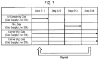
- FIG. 7 is a view illustrating a gas supply sequence when forming an AlN film according to an embodiment.
- the control part 6 of the first film forming apparatus 101 controls the heater 21 of the mounting table 2 so as to heat a wafer W to a predetermined temperature (e.g., 250 to 650 degrees C.).
- the control part 6 controls the pressure control valve of the exhaust mechanism 42 so as to adjust the inside of the processing container 1 to a predetermined pressure (e.g., 1.3 ⁇ 10 1 to 8.0 ⁇ 10 3 Pa).
- the control part 6 opens the valves 53 e and 57 e , and supplies a carrier gas (N 2 gas) of a predetermined flow rate (e.g., 100 to 10000 sccm) from the N 2 gas supply sources 53 a and 57 a to the gas supply lines 53 b and 57 b , respectively.
- the control part 6 supplies an Al-containing gas and NH 3 gas from the Al-containing gas supply source 51 a and the NH 3 gas supply source 55 a to the gas supply lines 51 b and 55 b , respectively.
- the valves 51 e and 55 e are closed, the Al-containing gas and the NH3 gas are respectively stored in the storage tanks 51 d and 55 d , and the pressure in the storage tanks 51 d and 55 d is increased.
- control part 6 opens the valve 51 e so as to supply the Al-containing gas stored in the storage tank 51 d into the processing container 1 , and causes a film made of the aluminum-containing material to be formed on the surface of the wafer W (step S 11 ).
- the control part 6 closes the valve 51 e so as to stop the supply of the Al-containing gas into the processing container 1 (step S 12 ).
- a predetermined time e.g., 0.05 to 5 seconds
- the control part 6 closes the valve 51 e so as to stop the supply of the Al-containing gas into the processing container 1 (step S 12 ).
- the control part 6 closes the valve 51 e so as to stop the supply of the Al-containing gas into the processing container 1 (step S 12 ).
- the control part 6 closes the valve 51 e so as to stop the supply of the Al-containing gas into the processing container 1 (step S 12 ).
- the control part 6 opens the valve 55 e so as to supply the NH 3 gas stored in the storage tank 55 d into the processing container 1 and to reduce the Al-containing gas adsorbed on the surface of the wafer W (step S 13 ).
- the control part 6 closes the valve 55 e so as to stop the supply of the NH 3 gas into the processing container 1 (step S 14 ).
- a predetermined time e.g., 0.05 to 5 seconds
- the control part 6 closes the valve 55 e so as to stop the supply of the NH 3 gas into the processing container 1 (step S 14 ).
- the NH 3 gas supplied from the NH 3 gas supply source 55 a to the gas supply line 55 b is stored in the storage tank 55 d , and the pressure in the storage tank 55 d is increased.
- the carrier gas (N 2 ) supplied from the gas supply line 53 b and the gas supply line 57 b also functions as a purge gas, and the excess Al-containing gas may be exhausted (step S 14 ).
- the control part 6 repeats the cycle of steps S 11 to S 14 for multiple cycles (e.g., 10 to 1000 cycles) so as to form an AlN film having a desired film thickness.
- AlCl 3 gas when used as the Al-containing gas, it reacts as follows: AlCl 3 +NH 3 ⁇ AlN+HCl ⁇ and AlN is adsorbed on the surface of the wafer W.
- TMA gas when used as the Al-containing gas, it reacts as follows: C 6 H 18 Al 2 +NH 3 ⁇ AlN+C x H y ⁇ and AlN is adsorbed on the surface of the wafer W.
- the gas supply sequence and the conditions of process gases when forming an AlN film shown in FIG. 7 are merely examples, and are not limited thereto. Other gas supply sequences and process conditions of process gases may be used to form an AlN film.
- FIG. 8 is a view illustrating a gas supply sequence when forming an initial tungsten film according to an embodiment.
- the control part 6 of the second film forming apparatus 102 controls the heater 21 of the mounting table 2 so as to heat a wafer W to a predetermined temperature (e.g., 250 to 650 degrees C.).
- the control part 6 controls the pressure control valve of the exhaust mechanism 42 so as to adjust the inside of the processing container 1 to a predetermined pressure (e.g., 1.3 ⁇ 10 1 to 8.0 ⁇ 10 3 Pa).
- the control part 6 opens the valves 63 e and 67 e , and supplies a carrier gas (N 2 gas) of a predetermined flow rate (e.g., 100 to 8000 sccm) from the N 2 gas supply sources 63 a and 67 a to the gas supply lines 63 b and 67 b , respectively.
- a carrier gas N 2 gas
- a predetermined flow rate e.g. 100 to 8000 sccm
- control part 6 opens the valve 61 e and supplies the WF 6 gas stored in the storage tank 61 d into the processing container 1 so as to be adsorbed on the surface of the wafer W (step S 21 ). Further, in parallel with the supply of the WF 6 gas into the processing container 1 , the control part 6 supplies the purge gas (N 2 gas) from the N 2 gas supply sources 62 a and 66 a to the gas supply lines 62 b and 66 b , respectively. At this time, by closing the valves 62 e and 66 e , the purge gas is stored in the storage tanks 62 d and 66 d , and the pressure in the storage tanks 62 d and 66 d is increased.
- purge gas N 2 gas
- the control part 6 closes the valve 61 e so as to stop the supply of the WF 6 gas into the processing container 1 .
- the control part 6 opens the valves 62 e and 66 e , and supplies the purge gas stored in each of the storage tanks 62 d and 66 d into the processing container 1 (step S 22 ).
- the purge gas is supplied from the storage tanks 62 d and 66 d in the state of increased pressure, the purge gas is supplied into the processing container 1 at a relatively large flow rate, for example, a flow rate (for example, 500 to 10000 sccm) larger than the flow rate of the carrier gas. Therefore, the WF 6 gas remaining in the processing container 1 is quickly discharged to the exhaust pipe 41 , and the atmosphere inside the processing container 1 is replaced from the WF 6 gas atmosphere to the atmosphere containing N 2 gas within a short time.
- a flow rate for example, 500 to 10000 sccm
- the WF 6 gas supplied from the metal material gas supply source 61 a to the gas supply line 61 b is stored in the storage tank 61 d , and the pressure in the storage tank 61 d is increased.
- the control part 6 closes the valves 62 e and 66 e so as to stop the supply of the purge gas into the processing container 1 .
- the control part 6 opens the valve 65 e and supplies the B 2 H 6 gas stored in the storage tank 65 d into the processing container 1 so as to reduce the WF 6 gas adsorbed on the surface of the wafer W (step S 23 ).
- the purge gas supplied from the N 2 gas supply sources 62 a and 66 a to the gas supply lines 62 b and 66 b are stored in the storage tanks 62 d and 66 d , and the pressure in the storage tanks 62 d and 66 d is increased.
- the control part 6 closes the valve 65 e so as to stop the supply of the B 2 H 6 gas into the processing container 1 .
- the control part 6 opens the valves 62 e and 66 e , and supplies the purge gas stored in each of the storage tanks 62 d and 66 d into the processing container 1 (step S 24 ).
- the purge gas is supplied from the storage tanks 62 d and 66 d in the state of increased pressure, the purge gas is supplied into the processing container 1 at a relatively large flow rate, for example, a flow rate (for example, 500 to 10000 sccm) larger than the flow rate of the carrier gas. Therefore, the B 2 H 6 gas remaining in the processing container 1 is quickly discharged to the exhaust pipe 41 , and the atmosphere inside the processing container 1 is replaced from the B 2 H 6 gas atmosphere to the atmosphere containing N 2 gas within a short time. Meanwhile, by closing the valve 65 e , the B 2 H 6 gas supplied from the boron-containing gas supply source 65 a to the gas supply line 65 b is stored in the storage tank 65 d , and the pressure in the storage tank 65 d is increased.
- a flow rate for example, 500 to 10000 sccm
- the control part 6 repeats the cycle of steps S 21 to S 24 for multiple cycles (e.g., 50 to 2000 cycles) so as to form an initial tungsten film having a desired film thickness.
- gas supply sequence and the conditions of process gases when forming an initial tungsten film shown in FIG. 8 are merely examples, and are not limited thereto. Other gas supply sequences and process conditions of process gases may be used to form the initial tungsten film.
- FIG. 9 is a view illustrating a gas supply sequence when forming a main tungsten film according to an embodiment.
- the control part 6 of the third film forming apparatus 103 controls the heater 21 of the mounting table 2 so as to heat a wafer W to a predetermined temperature (e.g., 250 to 650 degrees C.). In addition, the control part 6 controls the pressure control valve of the exhaust mechanism 42 so as to adjust the inside of the processing container 1 to a predetermined pressure (e.g., 1.3 ⁇ 10 1 to 8.0 ⁇ 10 3 Pa).
- the control part 6 opens the valves 63 e and 67 e , and supplies a carrier gas (N 2 gas) of a predetermined flow rate (e.g., 100 to 8000 sccm) from the N 2 gas supply sources 63 a and 67 a to the gas supply lines 63 b and 67 b , respectively.
- the control part 6 opens the valve 64 e , and supplies H 2 gas of a predetermined flow rate (e.g., 100 to 20000 sccm) from the H 2 gas supply sources 64 a to the gas supply lines 64 b .
- control part 6 supplies WF 6 gas and H 2 gas from the metal material gas supply source 61 a and the H 2 gas supply source 68 a to the gas supply lines 61 b and 68 b , respectively.
- the valves 61 e and 68 e are closed, the WF 6 gas and the H 2 gas are respectively stored in the storage tanks 61 d and 68 d , and the pressure in the storage tanks 61 d and 68 d is increased.
- control part 6 opens the valve 61 e and supplies the WF 6 gas stored in the storage tank 61 d into the processing container 1 so as to be adsorbed on the surface of the wafer W (step S 31 ). Further, in parallel with the supply of the WF 6 gas into the processing container 1 , the control part 6 supplies the purge gas (N 2 gas) from the N 2 gas supply sources 62 a and 66 a to the gas supply lines 62 b and 66 b , respectively. At this time, by closing the valves 62 e and 66 e , the purge gas is stored in the storage tanks 62 d and 66 d , and the pressure in the storage tanks 62 d and 66 d is increased.
- purge gas N 2 gas
- the control part 6 closes the valve 61 e so as to stop the supply of the WF 6 gas into the processing container 1 .
- the control part 6 opens the valves 62 e and 66 e , and supplies the purge gas stored in each of the storage tanks 62 d and 66 d into the processing container 1 (step S 32 ).
- the purge gas is supplied from the storage tanks 62 d and 66 d in the state of increased pressure, the purge gas is supplied into the processing container 1 at a relatively large flow rate, for example, a flow rate (for example, 500 to 10000 sccm) larger than the flow rate of the carrier gas. Therefore, the WF 6 gas remaining in the processing container 1 is quickly discharged to the exhaust pipe 41 , and the atmosphere inside the processing container 1 is replaced from the WF 6 gas atmosphere to the atmosphere containing H 2 gas and N 2 gas within a short time.
- a flow rate for example, 500 to 10000 sccm
- the WF 6 gas supplied from the metal material gas supply source 61 a to the gas supply line 61 b is stored in the storage tank 61 d , and the pressure in the storage tank 61 d is increased.
- the control part 6 closes the valves 62 e and 66 e so as to stop the supply of the purge gas into the processing container 1 .
- the control part 6 opens the valve 68 e and supplies the H 2 gas stored in the storage tank 68 d into the processing container 1 so as to reduce the WF 6 gas adsorbed on the surface of the wafer W (step S 33 ).
- the purge gas supplied from the N 2 gas supply sources 62 a and 66 a to the gas supply lines 62 b and 66 b are stored in the storage tanks 62 d and 66 d , and the pressure in the storage tanks 62 d and 66 d is increased.
- the control part 6 closes the valve 68 e so as to stop the supply of the H 2 gas into the processing container 1 .
- the control part 6 opens the valves 62 e and 66 e , and supplies the purge gas stored in each of the storage tanks 62 d and 66 d into the processing container 1 (step S 34 ).
- the purge gas is supplied from the storage tanks 62 d and 66 d in the state of increased pressure, the purge gas is supplied into the processing container 1 at a relatively large flow rate, for example, a flow rate (for example, 500 to 10000 sccm) larger than the flow rate of the carrier gas. Therefore, the H 2 gas remaining in the processing container 1 is quickly discharged to the exhaust pipe 41 , and the atmosphere inside the processing container 1 is replaced from the H 2 gas atmosphere to the atmosphere containing H 2 gas and N 2 gas within a short time. Meanwhile, by closing the valve 68 e , the H 2 gas supplied from the H 2 gas supply source 68 a to the gas supply line 68 b is stored in the storage tank 68 d , and the pressure in the storage tank 68 d is increased.
- a flow rate for example, 500 to 10000 sccm
- the control part 6 repeats the cycle of steps S 31 to S 34 for multiple cycles (e.g., 50 to 2000 cycles) so as to form a main tungsten film having a desired film thickness.
- gas supply sequence and the conditions of process gases when forming a main tungsten film shown in FIG. 9 are merely examples, and are not limited thereto. Other gas supply sequences and process conditions of process gases may be used to form the main tungsten film.
- FIG. 10 is a view illustrating an example of the layer configuration of a wafer according to the present embodiment.
- FIG. 10 illustrates an example of the layer configuration of a wafer W formed by the film forming method according to the present embodiment.
- an AlO layer is formed on a silicon (SiO 2 ) layer for blocking, and a TiN film having a thickness of, for example, 1 nm is formed on the AlO layer for the sake adhesion and reaction suppression.
- an AlN film having a thickness of, for example, 1 nm is formed on the TiN film by the film forming method according to the present embodiment, and a tungsten nucleation film (Nuc) having a thickness of, for example, 1 nm is formed on the AlN film as an initial tungsten film.
- a low-resistance main tungsten film (W) is formed on the nucleation film.
- the AlN film is able to cancel the orientation of the TiN film.
- the thickness of the AlN film is preferably about 1 to 2 nm. With the thickness of about 1 nm, it is possible to cancel the orientation of the base TiN film.
- the Nucleation film by forming the Nucleation film on the wafer W, it is possible to enhance the adhesion of tungsten film to be formed. In addition, it is possible to improve the uniformity of the tungsten film to be formed.
- the thickness of the nucleation film is preferably about 0.5 to 5 nm.
- FIG. 11 is a view illustrating an example of the layer configuration of a wafer according to a first comparative example.
- FIG. 11 illustrates an example of the layer configuration of a conventional wafer W as a first comparative example.
- an AlO layer is formed on a silicon (SiO 2 ) layer for blocking, and a TiN film having a thickness of, for example, 2 nm is formed on the AlO layer for the sake of adhesion and reaction suppression.
- a tungsten nucleation film (Nuc) having a thickness of, for example, 3 nm is formed on the TiN film.
- a low-resistance tungsten film (W) is formed on the nucleation film.
- FIG. 12 is a view illustrating an example of a change in resistivity with respect to a thickness of a tungsten film.
- FIG. 12 shows changes in resistivity with respect to thicknesses of tungsten films in the layer configuration of the present embodiment shown in FIG. 10 and the layer configuration of the first comparative example illustrated in FIG. 11 .
- the thickness of each tungsten film is measured from the interface with the TiN film. That is, in the layer configuration of the present embodiment, the thicknesses of the AlN film, the nucleation film (Nuc), and the tungsten film (W) are taken as the thickness of the tungsten film.
- the thicknesses of the AlN film, the nucleation film (Nuc), and the tungsten film (W) are taken as the thickness of the tungsten film.
- the resistivity is shown normalized with reference to the resistivity of the first comparative example in the case where the thickness is 10 nm. As shown in FIG. 12 , when the thickness is 10 nm, the resistivity in the layer configuration of the present embodiment is reduced by 59% compared that in the layer configuration of the first comparative example. In addition, when the thickness is 15 nm, the resistivity of the layer configuration of the present embodiment is reduced by 41% compared with the layer configuration of the first comparative example.
- a wiring line is miniaturized, and a reduction in resistance in the wiring line is required.
- a tungsten film is formed as a word line, further reduction in resistance of the tungsten film is required for miniaturization.
- the applicant has found that it is possible to reduce stress in a metal layer by forming an initial metal film by supplying a metal material gas and a boron-containing gas to a substrate having a cancel layer formed on a base film, and forming a main metal film on the initial metal film.
- the stress in a tungsten layer is reduced by supplying WF 6 gas and B 2 H 6 gas to a wafer W having an MN film formed on a TiN film to form an initial tungsten film, and forming a main tungsten film on the substrate on which the initial tungsten film is formed, as in the present embodiment.
- SiH 4 gas is supplied instead of B 2 H 6 gas so as to form a second comparative example.
- FIG. 13 is a view illustrating an example of the comparison result of stress in a tungsten layer according to an embodiment.
- FIG. 13 shows a comparison result between the stress in the layer configuration of the present embodiment and the stress in the layer configuration of the second comparative example.
- the stress in the tungsten layer is 0.1 GPa or less.
- the stress in the tungsten layer is 1.8 GPa or more.
- the stress is significantly reduced compared with that in the layer configuration of the second comparative example.
- stress is reduced in the wafer W, for example, the occurrence of deformation such as warpage is suppressed.
- FIG. 14 is a view illustrating an example of a change in resistivity with respect to the thickness of a tungsten film according to an embodiment.
- FIG. 14 shows changes in resistivity with respect to thicknesses of the tungsten film in the layer configuration of the present embodiment and the layer configuration of the second comparative example.
- a cancel layer is formed on a wafer W, which is disposed in the processing container 1 and on which a base film (TiN film) is formed, so as to cancel the orientation of a base film.
- an initial metal film is formed by supplying a metal material gas and a boron-containing gas to the wafer W on which the cancel layer is formed.
- a main metal film is formed on the wafer W on which the initial metal film is formed.
- the film forming method according to the present embodiment includes any of WF 6 and WCl x as the metal material gas, and includes any of B 2 H 6 and BCl as the boron-containing gas.
- the film forming method according to the present embodiment it is possible to form a tungsten film.
- the thickness of the initial metal film is set to 0.5 to 5 nm.
- the metal to be formed as a film is tungsten
- the main metal film is formed by supplying a W-containing gas and an H-containing gas.
- the W-containing gas includes any of WF 6 and WCl x and the H-containing gas includes any of H 2 , SiH 4 , and B 2 H 6 .
- the film forming method according to the present embodiment it is possible to form a main tungsten film having low stress.
- the initial tungsten film and the main tungsten film may be formed in the same film forming apparatus.
- the second film forming apparatus 102 and the third film forming apparatus 103 may form the initial tungsten film and the main tungsten film.
- FIG. 15 is a cross-sectional view illustrating an example of a schematic configuration of a film forming apparatus according to another embodiment.
- the second film forming apparatus 102 illustrated in FIG. 15 has the configuration of the gas supply mechanism 5 illustrated in FIG. 4 in addition to the configuration of the gas supply mechanism 5 illustrated in FIG. 3 .
- the film forming system 100 by forming the initial tungsten film and the main tungsten film in the second film forming apparatus 102 and the third film forming apparatus 103 , respectively, it is possible to eliminate the transfer time of the wafer W between the film forming apparatuses between the film formation of the initial tungsten film and the main tungsten film, and thus productivity is improved.
- the base film is formed by the base-film forming apparatus 201 and the cancel layer is formed by the first film forming apparatus 101 has been described by way of an example, but the present disclosure is not limited thereto.
- the base film and the cancel layer may be formed in the same film forming apparatus.
- the base film, the cancel layer, initial tungsten film, and the main tungsten film may be formed in the same film forming apparatus. In this case, it is possible to eliminate the transfer time of the wafer W between the film forming apparatuses, and thus productivity is improved.
- the base film is formed by the base-film forming apparatus 201 and the cancel layer is formed by the first film forming apparatus 101 has been described by way of an example, but the present disclosure is not limited thereto.
- the base film may be formed in a base-film forming apparatus in another film forming system.
- the base film is formed by the base-film forming apparatus 201 and the cancel layer is formed by the first film forming apparatus 101 has been described by way of an example, but the present disclosure is not limited thereto.
- the number of film forming apparatuses may be appropriately changed in consideration of productivity and the like.
- the semiconductor wafer may be silicon or a compound semiconductor such as GaAs, SiC, or GaN.
- the substrate is not limited to the semiconductor wafer, and may be applied to a glass substrate used for FPD (flat panel display) such as a liquid crystal display device, a ceramic substrate, and the like.
Landscapes
- Chemical & Material Sciences (AREA)
- General Chemical & Material Sciences (AREA)
- Chemical Kinetics & Catalysis (AREA)
- Engineering & Computer Science (AREA)
- Materials Engineering (AREA)
- Mechanical Engineering (AREA)
- Metallurgy (AREA)
- Organic Chemistry (AREA)
- Inorganic Chemistry (AREA)
- Chemical Vapour Deposition (AREA)
- Electrodes Of Semiconductors (AREA)
Abstract
Description
-
- AlN film
- Temperature: 250 to 550 degrees C.
- Pressure: 0.1 to 10 Torr
- Al-containing gas: 10 to 500 sccm
- Carrier gas (N2): 1000 to 10000 sccm
- Purge gas (N2): 0 to 10000 sccm
- NH3 gas: 1000 to 10000 sccm
- Time:
- Al-containing gas: 0.05 to 5 sec
- Purge: 0.05 to 5 sec
- NH3 gas: 0.05 to 5 sec
- Purge: 0.05 to 5 sec
- Initial tungsten film (nucleation film):
- Temperature: 150 to 550 degrees C.
- Pressure: 1 to 100 Torr
- W-containing gas: 10 to 500 sccm
- Carrier gas (N2): 1000 to 10000 sccm
- Purge gas (N2): 0 to 10000 sccm
- B2H6 gas: 10 to 1000 sccm
- Time:
- W-containing gas: 0.05 to 15 sec
- Purge: 0.05 to 15 sec
- B2H6 gas: 0.05 to 15 sec
- Purge: 0.05 to 15 sec
- Main tungsten film
- Temperature: 250 to 550 degrees C.
- Pressure: 0.1 to 20 Torr
- W-containing gas: 100 to 500 sccm
- Carrier gas (N2): 1000 to 10000 sccm
- Purge gas (N2): 0 to 10000 sccm
- H2 gas: 500 to 20000 sccm
- Time:
- W-containing gas: 0.05 to 15 sec
- Purge: 0.05 to 15 sec
- H2 gas: 0.05 to 15 sec
- Purge: 0.05 to 15 sec
-
- Nucleation Film
- Temperature: 150 to 550 degrees C.
- Pressure: 1 to 100 Torr
- W-containing gas: 10 to 500 sccm
- Carrier gas (N2): 1000 to 10000 sccm
- Purge gas (N2): 0 to 10000 sccm
- H2 gas: 500 to 20000 sccm
- SiH4 gas: 10 to 1000 sccm
- Time:
- W-containing gas: 0.05 to 15 sec
- Purge: 0.05 to 15 sec
- SiH4 gas: 0.05 to 15 sec
- Purge: 0.05 to 15 sec
- W Film
- Temperature: 250 to 550 degrees C.
- Pressure: 0.1 to 20 Torr
- W-containing gas: 100 to 500 sccm
- Carrier gas (N2): 1000 to 10000 sccm
- Purge gas (N2): 0 to 10000 sccm
- H2 gas: 500 to 20000 sccm
- Time:
- W-containing gas: 0.05 to 15 sec
- Purge: 0.05 to 15 sec
- H2gas: 0.05 to 15 sec
- Purge: 0.05 to 15 sec
Claims (14)
Applications Claiming Priority (3)
| Application Number | Priority Date | Filing Date | Title |
|---|---|---|---|
| JPJP2018-163400 | 2018-08-31 | ||
| JP2018163400A JP7138518B2 (en) | 2018-08-31 | 2018-08-31 | Film forming method and film forming system |
| JP2018163400 | 2018-08-31 |
Publications (2)
| Publication Number | Publication Date |
|---|---|
| US20200071829A1 US20200071829A1 (en) | 2020-03-05 |
| US11401609B2 true US11401609B2 (en) | 2022-08-02 |
Family
ID=69642296
Family Applications (1)
| Application Number | Title | Priority Date | Filing Date |
|---|---|---|---|
| US16/553,602 Active 2040-03-05 US11401609B2 (en) | 2018-08-31 | 2019-08-28 | Film forming method and film forming system |
Country Status (3)
| Country | Link |
|---|---|
| US (1) | US11401609B2 (en) |
| JP (1) | JP7138518B2 (en) |
| KR (1) | KR102307268B1 (en) |
Families Citing this family (3)
| Publication number | Priority date | Publication date | Assignee | Title |
|---|---|---|---|---|
| JP7647185B2 (en) * | 2021-03-09 | 2025-03-18 | 東京エレクトロン株式会社 | Method and system for depositing tungsten films |
| TWI860640B (en) * | 2023-03-07 | 2024-11-01 | 環球晶圓股份有限公司 | Fabrication method of epitaxial structure |
| KR102610272B1 (en) | 2023-05-24 | 2023-12-06 | (주)금호전력 | Rail bond implemented as jig type |
Citations (7)
| Publication number | Priority date | Publication date | Assignee | Title |
|---|---|---|---|---|
| JP2004536225A (en) | 2001-07-16 | 2004-12-02 | アプライド マテリアルズ インコーポレイテッド | Method and apparatus for depositing tungsten after surface treatment to improve film properties |
| KR100557964B1 (en) | 2004-10-22 | 2006-03-07 | 주식회사 하이닉스반도체 | Method for forming metal 1 contact of semiconductor device |
| KR20080101745A (en) | 2007-05-15 | 2008-11-21 | 어플라이드 머티어리얼스, 인코포레이티드 | Atomic Layer Deposition of Tungsten Materials |
| JP2011151356A (en) | 2009-12-22 | 2011-08-04 | Hitachi Kokusai Electric Inc | Method of manufacturing semiconductor device, method of processing substrate, and substrate processing apparatus |
| JP2017008412A (en) | 2015-05-27 | 2017-01-12 | ラム リサーチ コーポレーションLam Research Corporation | Low fluorine tungsten deposition by subsequent cvd process |
| US20190221434A1 (en) * | 2018-01-18 | 2019-07-18 | Tokyo Electron Limited | Tungsten film forming method, film forming system and film forming apparatus |
| JP2019160918A (en) | 2018-03-09 | 2019-09-19 | 東芝メモリ株式会社 | Semiconductor device and manufacturing method thereof |
Family Cites Families (2)
| Publication number | Priority date | Publication date | Assignee | Title |
|---|---|---|---|---|
| JP6706903B2 (en) * | 2015-01-30 | 2020-06-10 | 東京エレクトロン株式会社 | Method for forming tungsten film |
| JP2018043090A (en) * | 2017-12-22 | 2018-03-22 | 株式会社三洋物産 | Game machine |
-
2018
- 2018-08-31 JP JP2018163400A patent/JP7138518B2/en active Active
-
2019
- 2019-08-28 KR KR1020190105710A patent/KR102307268B1/en active Active
- 2019-08-28 US US16/553,602 patent/US11401609B2/en active Active
Patent Citations (7)
| Publication number | Priority date | Publication date | Assignee | Title |
|---|---|---|---|---|
| JP2004536225A (en) | 2001-07-16 | 2004-12-02 | アプライド マテリアルズ インコーポレイテッド | Method and apparatus for depositing tungsten after surface treatment to improve film properties |
| KR100557964B1 (en) | 2004-10-22 | 2006-03-07 | 주식회사 하이닉스반도체 | Method for forming metal 1 contact of semiconductor device |
| KR20080101745A (en) | 2007-05-15 | 2008-11-21 | 어플라이드 머티어리얼스, 인코포레이티드 | Atomic Layer Deposition of Tungsten Materials |
| JP2011151356A (en) | 2009-12-22 | 2011-08-04 | Hitachi Kokusai Electric Inc | Method of manufacturing semiconductor device, method of processing substrate, and substrate processing apparatus |
| JP2017008412A (en) | 2015-05-27 | 2017-01-12 | ラム リサーチ コーポレーションLam Research Corporation | Low fluorine tungsten deposition by subsequent cvd process |
| US20190221434A1 (en) * | 2018-01-18 | 2019-07-18 | Tokyo Electron Limited | Tungsten film forming method, film forming system and film forming apparatus |
| JP2019160918A (en) | 2018-03-09 | 2019-09-19 | 東芝メモリ株式会社 | Semiconductor device and manufacturing method thereof |
Also Published As
| Publication number | Publication date |
|---|---|
| US20200071829A1 (en) | 2020-03-05 |
| KR20200026111A (en) | 2020-03-10 |
| JP7138518B2 (en) | 2022-09-16 |
| JP2020033630A (en) | 2020-03-05 |
| KR102307268B1 (en) | 2021-09-29 |
Similar Documents
| Publication | Publication Date | Title |
|---|---|---|
| US10400330B2 (en) | Tungsten film forming method and storage medium | |
| JP2016225396A (en) | Stress reduction method of metal film and film forming method of metal film | |
| US10910225B2 (en) | Film forming method | |
| US11551933B2 (en) | Substrate processing method and substrate processing apparatus | |
| US20210115560A1 (en) | Film forming method, film forming system, and film forming apparatus | |
| US11401609B2 (en) | Film forming method and film forming system | |
| KR20200097646A (en) | Substrate processing method and film forming system | |
| US10784110B2 (en) | Tungsten film forming method, film forming system and film forming apparatus | |
| US11171004B2 (en) | Film forming method and substrate processing system | |
| US12119219B2 (en) | Film forming method, method for manufacturing semiconductor device, film forming device, and system for manufacturing semiconductor device | |
| US11970767B2 (en) | Film forming method and film forming apparatus | |
| US20200118824A1 (en) | Film forming method and substrate processing system | |
| US11549179B2 (en) | Film forming method | |
| US20240003002A1 (en) | Tungsten Film-Forming Method, Film-Forming System and Storage Medium | |
| US20200056287A1 (en) | Film-Forming Method and Film-Forming Apparatus | |
| US20250369109A1 (en) | Film forming method and film forming apparatus | |
| KR20220124223A (en) | Film-forming method, film-forming apparatus, and manufacturing method of a semiconductor device |
Legal Events
| Date | Code | Title | Description |
|---|---|---|---|
| AS | Assignment |
Owner name: TOKYO ELECTRON LIMITED, JAPAN Free format text: ASSIGNMENT OF ASSIGNORS INTEREST;ASSIGNORS:MAEKAWA, KOJI;YAMAGUCHI, KATSUMASA;SAMESHIMA, TAKASHI;REEL/FRAME:050202/0387 Effective date: 20190805 |
|
| FEPP | Fee payment procedure |
Free format text: ENTITY STATUS SET TO UNDISCOUNTED (ORIGINAL EVENT CODE: BIG.); ENTITY STATUS OF PATENT OWNER: LARGE ENTITY |
|
| STPP | Information on status: patent application and granting procedure in general |
Free format text: NON FINAL ACTION MAILED |
|
| STPP | Information on status: patent application and granting procedure in general |
Free format text: RESPONSE TO NON-FINAL OFFICE ACTION ENTERED AND FORWARDED TO EXAMINER |
|
| STPP | Information on status: patent application and granting procedure in general |
Free format text: NOTICE OF ALLOWANCE MAILED -- APPLICATION RECEIVED IN OFFICE OF PUBLICATIONS |
|
| STPP | Information on status: patent application and granting procedure in general |
Free format text: NOTICE OF ALLOWANCE MAILED -- APPLICATION RECEIVED IN OFFICE OF PUBLICATIONS |
|
| STCF | Information on status: patent grant |
Free format text: PATENTED CASE |
|
| MAFP | Maintenance fee payment |
Free format text: PAYMENT OF MAINTENANCE FEE, 4TH YEAR, LARGE ENTITY (ORIGINAL EVENT CODE: M1551); ENTITY STATUS OF PATENT OWNER: LARGE ENTITY Year of fee payment: 4 |