US11399701B2 - Receptacle module and medical device - Google Patents
Receptacle module and medical device Download PDFInfo
- Publication number
- US11399701B2 US11399701B2 US16/258,978 US201916258978A US11399701B2 US 11399701 B2 US11399701 B2 US 11399701B2 US 201916258978 A US201916258978 A US 201916258978A US 11399701 B2 US11399701 B2 US 11399701B2
- Authority
- US
- United States
- Prior art keywords
- receptacle
- circuit unit
- substrate
- patient
- patient circuit
- Prior art date
- Legal status (The legal status is an assumption and is not a legal conclusion. Google has not performed a legal analysis and makes no representation as to the accuracy of the status listed.)
- Active, expires
Links
Images


Classifications
-
- A—HUMAN NECESSITIES
- A61—MEDICAL OR VETERINARY SCIENCE; HYGIENE
- A61B—DIAGNOSIS; SURGERY; IDENTIFICATION
- A61B1/00—Instruments for performing medical examinations of the interior of cavities or tubes of the body by visual or photographical inspection, e.g. endoscopes; Illuminating arrangements therefor
- A61B1/04—Instruments for performing medical examinations of the interior of cavities or tubes of the body by visual or photographical inspection, e.g. endoscopes; Illuminating arrangements therefor combined with photographic or television appliances
- A61B1/045—Control thereof
-
- A—HUMAN NECESSITIES
- A61—MEDICAL OR VETERINARY SCIENCE; HYGIENE
- A61B—DIAGNOSIS; SURGERY; IDENTIFICATION
- A61B1/00—Instruments for performing medical examinations of the interior of cavities or tubes of the body by visual or photographical inspection, e.g. endoscopes; Illuminating arrangements therefor
- A61B1/00112—Connection or coupling means
- A61B1/00114—Electrical cables in or with an endoscope
-
- G—PHYSICS
- G06—COMPUTING OR CALCULATING; COUNTING
- G06F—ELECTRIC DIGITAL DATA PROCESSING
- G06F1/00—Details not covered by groups G06F3/00 - G06F13/00 and G06F21/00
- G06F1/16—Constructional details or arrangements
- G06F1/18—Packaging or power distribution
- G06F1/181—Enclosures
- G06F1/182—Enclosures with special features, e.g. for use in industrial environments; grounding or shielding against radio frequency interference [RFI] or electromagnetical interference [EMI]
-
- H—ELECTRICITY
- H05—ELECTRIC TECHNIQUES NOT OTHERWISE PROVIDED FOR
- H05K—PRINTED CIRCUITS; CASINGS OR CONSTRUCTIONAL DETAILS OF ELECTRIC APPARATUS; MANUFACTURE OF ASSEMBLAGES OF ELECTRICAL COMPONENTS
- H05K9/00—Screening of apparatus or components against electric or magnetic fields
- H05K9/0007—Casings
- H05K9/002—Casings with localised screening
- H05K9/0022—Casings with localised screening of components mounted on printed circuit boards [PCB]
- H05K9/0024—Shield cases mounted on a PCB, e.g. cans or caps or conformal shields
-
- A—HUMAN NECESSITIES
- A61—MEDICAL OR VETERINARY SCIENCE; HYGIENE
- A61B—DIAGNOSIS; SURGERY; IDENTIFICATION
- A61B1/00—Instruments for performing medical examinations of the interior of cavities or tubes of the body by visual or photographical inspection, e.g. endoscopes; Illuminating arrangements therefor
- A61B1/00112—Connection or coupling means
- A61B1/00121—Connectors, fasteners and adapters, e.g. on the endoscope handle
Definitions
- the present disclosure relates to a receptacle module and a medical device.
- a patient circuit is normally configured as a floating circuit which is not protectively grounded. Therefore, the patient circuit functions as an antenna, and thus noise from the outside to the patient circuit is easily mixed or noise from the patient circuit to the outside is easily transmitted. Therefore, in the medical device (an endoscope imaging device) disclosed in JP 2-193634 A, a patient circuit unit conducted to a distal end device is shielded in a shielding member (a patient circuit unit shielding case) in a patient circuit including the distal end device.
- a shielding member a patient circuit unit shielding case
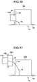
- FIGS. 16 and 17 are diagrams illustrating a problem in a medical device of the related art.
- receptacle modules 12 E and 12 F in which a receptacle 131 E detachably connected to a connector of a distal end device such as an electronic scope and a patient substrate 14 E are arranged are configured, for example, configurations illustrated in FIGS. 16 and 17 are considered.
- the receptacle module 12 E illustrated in FIG. 16 includes a receptacle substrate 13 E, the patient substrate 14 E, and a shielding member 15 E.
- the receptacle substrate 13 E is a printed substrate in which a wiring pattern is provided and the receptacle 131 E is mounted to be conducted to the wiring pattern.
- the patient substrate 14 E is a printed substrate in which a wiring pattern is provided and an electronic component is mounted to be conducted to the wiring pattern. As illustrated in FIG. 16 , the patient substrate 14 E is disposed at a posture orthogonal to the receptacle substrate 13 E. The wiring pattern provided in the patient substrate 14 E is conducted to a wiring pattern provided in the receptacle substrate 13 E via a harness Ha ( FIG. 16 ).
- the wiring pattern provided on the receptacle substrate 13 E, the wiring pattern or the electronic component provided on the patient substrate 14 E, and the harness Ha function as a patient circuit unit that is conducted to the distal end device in the patient circuit including the distal end device.
- the shielding member 15 E is formed of a conductive material, has an overall substantially rectangular parallelepiped shape, and has one side surface opened in a container shape.
- an opening 154 FIG. 16 ) for inserting the receptacle 131 E is formed in a side surface of the container shape.
- the shielding member 15 E is mounted so that the opened portion with the container shape is fitted on a surface on which the wiring pattern or an electronic component is provided on the patient substrate 14 E in a state in which the receptacle 131 E is inserted through the opening 154 , and shields the patient circuit unit.
- the opening 154 is formed in the shielding member 15 E.
- the shielding member 15 E In consideration of an assembly property of the receptacle module 12 E, it is necessary to separate the shielding member 15 E into two bodies or the like. Therefore, there is a problem that the structure of the shielding member 15 E may become complicated.
- the receptacle module 12 F illustrated in FIG. 17 is considered to be adopted.
- the receptacle module 12 F includes the receptacle substrate 13 E, the patient substrate 14 E, and a first shielding member 15 F 1 , and a second shielding member 15 F 2 .
- Each of the first shielding member 15 F 1 and the second shielding member 15 F 2 is formed of a conductive material, has an overall substantially rectangular parallelepiped shape, and has one side surface opened in a container shape. As illustrated in FIG. 17 , the first shielding member 15 F 1 is mounted so that the opened portion is fitted on an opposite surface of the surface on which the receptacle 131 E is mounted on the receptacle substrate 13 E and shields a wiring pattern (patient circuit unit) provided on the receptacle substrate 13 E.
- the second shielding member 15 F 2 is mounted so that the opened portion is fitted on the surface on which the wiring pattern or the electronic component is provided on the patient substrate 14 E and shields the wiring pattern or the electronic component (the patient circuit unit) provided in the patient substrate 14 E.
- the wiring pattern provided on the receptacle substrate 13 E and the wiring pattern provided on the patient substrate 14 E are conducted to each other via the harness Ha ( FIG. 17 ) passing through openings 155 and 156 ( FIG. 17 ) formed in the first shielding member 15 F 1 and the second shielding member 15 F 2 .
- a part of the harness Ha is located outside the first shielding member 15 F 1 and the second shielding member 15 F 2 . Therefore, the part of the harness Ha located outside the first shielding member 15 F 1 and the second shielding member 15 F 2 functions as an antenna, and thus noise from the outside to the part (the patient circuit unit) of the harness Ha is easily mixed or noise from the part (the patient circuit unit) of the harness Ha to the outside is easily transmitted. That is, there is a problem that a shielding property is inferior.
- a receptacle module for detachably connecting a connector of a distal end device coming into contact with or inserted into a subject
- the receptacle module including: a receptacle substrate including a first surface on which a receptacle to which the connector is detachably connected is mounted, and a second surface on an opposite side of the first surface; a patient circuit unit conducted to the distal end device via the receptacle; and a conductive shielding member mounted on the second surface and configured to shield the patient circuit unit from the opposite side.
- FIG. 1 is a diagram illustrating a schematic configuration of an endoscope device according to an embodiment
- FIG. 2 is a diagram illustrating examples of a primary circuit, a secondary circuit, and a patient circuit in the endoscope device;
- FIG. 3 is a diagram illustrating a receptacle module
- FIG. 4 is a diagram illustrating the receptacle module
- FIG. 5 is a diagram illustrating the receptacle module
- FIG. 6 is a diagram illustrating a receptacle substrate
- FIG. 7 is a diagram illustrating a first modification example of the embodiment.
- FIG. 8 is a diagram illustrating a second modification example of the embodiment.
- FIG. 9 is a diagram illustrating a third modification example of the embodiment.
- FIG. 10 is a diagram illustrating the third modification example of the embodiment.
- FIG. 11 is a diagram illustrating a fourth modification example of the embodiment.
- FIG. 12 is a diagram illustrating the fourth modification example of the embodiment.
- FIG. 13 is a diagram illustrating a fifth modification example of the embodiment.
- FIG. 14 is a diagram illustrating the fifth modification example of the embodiment.
- FIG. 15 is a diagram illustrating the fifth modification example of the embodiment.
- FIG. 16 is a diagram illustrating a problem in a medical device of the related art.
- FIG. 17 is a diagram illustrating the problem in the medical device of the related art.
- FIG. 1 is a diagram illustrating a schematic configuration of an endoscope device 1 according to an embodiment.
- the endoscope device 1 is equivalent to a medical device according to the present disclosure.
- the endoscope device 1 is used in medical fields and is a device that observes a subject such as the inside of a biological body.
- the endoscope device 1 includes an insertion unit 2 , a light source device 3 , a light guide 4 , a camera head 5 , a first transmission cable 6 , a display device 7 , a second transmission cable 8 , a control device 9 , and a third transmission cable 10 , as illustrated in FIG. 1 .
- the insertion unit 2 is configured as a rigid endoscope. That is, the insertion unit 2 has an elongated shape of which the entirety is rigid or at least a part is flexible and is inserted into a biological body.
- an optical system that is configured by one lens or a plurality of lenses and condenses a subject image is provided.
- the light source device 3 is connected to one end of the light guide 4 and supplies illumination light for illuminating the biological body to the one end of the light guide 4 under the control of the control device 9 .
- One end of the light guide 4 is detachably connected to the light source device 3 and the other end of the light guide 4 is detachably connected to the insertion unit 2 . Then, the light guide 4 delivers the light supplied from the light source device 3 from the one end to the other end to supply the light to the insertion unit 2 .
- the light supplied to the insertion unit 2 is emitted from the distal end of the insertion unit 2 to be radiated to the inside of the biological body.
- the light (subject image) radiated to the biological body and reflected from the biological body is condensed by the optical system inside the insertion unit 2 .
- the camera head 5 is detachably connected to a proximal end (an eyepiece 2 a ( FIG. 1 )) of the insertion unit 2 .
- the camera head 5 captures a subject image condensed in the insertion unit 2 and outputs an image signal (RAW signal) obtained through the imaging under the control of the control device 9 .
- the image signal is an image signal with 4K or more.
- the first transmission cable 6 includes connectors CN 1 and CN 2 at both ends, the connector CN 1 ( FIG. 1 ) at one end is detachably connected to the control device 9 , and the connector CN 2 ( FIG. 1 ) at the other end is detachably connected to the camera head 5 .
- the first transmission cable 6 transmits an image signal output from the camera head 5 to the control device 9 and transmits a control signal, a synchronization signal, a clock, driving power, and the like output from the control device 9 to the camera head 5 .
- the transmission of the image signal from the camera head 5 to the control device 9 via the first transmission cable 6 may be transmission of the image signal realized by an optical signal or may be transmission of an image signal realized by the electric signal. The same applies to the transmission of the control signal, the synchronization signal, and the clock from the control device 9 to the camera head 5 via the first transmission cable 6 .
- the insertion unit 2 , the camera head 5 , and the first transmission cable 6 described above are equivalent to a distal end device 11 ( FIG. 1 ) according to the present disclosure.
- the control device 9 includes a central processing unit (CPU) and the like and comprehensively controls operations of the light source device 3 , the camera head 5 , and the display device 7 .
- CPU central processing unit
- control device 9 generates a video signal by performing a predetermined process on the image signal acquired from the camera head 5 via the first transmission cable 6 and outputs the video signal to the display device 7 via the second transmission cable 8 . Then, the display device 7 displays an image based on the video signal.
- the control device 9 outputs a control signal or the like to the camera head 5 or the light source device 3 via the first transmission cable 6 and the third transmission cable 10 .
- the above-described control device 9 includes a receptacle module 12 ( FIG. 1 ) to which the connector CN 1 of the distal end device 11 is detachably connected.
- the detailed configuration of the receptacle module 12 will be described later.
- One end of the third transmission cable 10 is detachably connected to the light source device 3 and the other end thereof is detachably connected to the control device 9 . Then, the third transmission cable 10 transmits a control signal from the control device 9 to the light source device 3 .
- FIG. 2 is a diagram illustrating a primary circuit 100 , a secondary circuit 200 , and a patient circuit 300 in the endoscope device 1 .
- three circuits (the primary circuit 100 , the secondary circuit 200 , and the patient circuit 300 ) are broadly provided.
- the primary circuit 100 is provided inside the control device 9 and is connected to a commercial power supply via an inlet 101 . Then, the primary circuit 100 performs power supply to each of the secondary circuit 200 and the patient circuit 300 .
- the secondary circuit 200 is provided inside the control device 9 and includes, for example, a signal processor (not illustrated) that performs a predetermined process on an image signal acquired from the camera head 5 and the like.
- the secondary circuit 200 is supplied with power from the primary circuit 100 via a first insulation transformer IT 1 ( FIG. 2 ). That is, the primary circuit 100 is electrically insulated from the secondary circuit 200 .
- the secondary circuit 200 is protectively grounded.
- the patient circuit 300 is an electric circuit for which a biological body itself serves as a part of the circuit when the distal end device 11 comes into contact with the biological body, is provided inside the distal end device 11 and the control device 9 , and includes, for example, an image sensor (not illustrated) that captures a subject image condensed in the insertion unit 2 , or the like.
- the patient circuit 300 is supplied with power from the primary circuit 100 via a second insulation transformer IT 2 ( FIG. 2 ). That is, the primary circuit 100 is electrically insulated from the patient circuit 300 .
- the patient circuit 300 is electrically insulated from the secondary circuit 200 .
- the secondary circuit 200 and the patient circuit 300 are connected to an insulation device 400 via a first impedance element Im 1 provided in the secondary circuit 200 and a second impedance element Im 2 provided in the patient circuit 300 .
- the first impedance element Im 1 and the second impedance element Im 2 capacitors, coils, resistors, or the like may be exemplified.
- the insulation device 400 for example, a photocoupler, a high-frequency transformer, or the like may be exemplified.
- an image signal, a control signal, a synchronization signal, a clock, and the like are transmitted via the insulation device 400 .
- FIGS. 3 to 5 are diagrams illustrating the receptacle module 12 .
- FIG. 3 is a perspective view illustrating the overall receptacle module 12 .
- FIG. 4 is an exploded perspective view illustrating the receptacle module 12 illustrated in FIG. 3 .
- FIG. 5 is a diagram illustrating the receptacle module 12 when viewed from the side and is a diagram schematically illustrating the inside of the shielding member 15 .
- An arrow illustrated in FIG. 3 indicates an insertion direction of the connector CN 1 into a receptacle 131 .
- the patient circuit 300 and the insulation device 400 are indicated by solid lines, the secondary circuit 200 is illustrated by a one-dot chain line, and a second connection connector 135 is not illustrated.
- the receptacle module 12 includes a receptacle substrate 13 , a patient substrate 14 ( FIGS. 4 and 5 ), and the shielding member 15 , as illustrated in FIGS. 3 to 5 .
- FIG. 6 is a diagram illustrating the receptacle substrate 13 . Specifically, FIG. 6 is diagram illustrating the receptacle substrate 13 when viewed from the side of a surface 13 b opposite to a surface 13 a on which the receptacle 131 is mounted.
- the receptacle substrate 13 is formed of an insulation material such as a glass epoxy resin and is a plate that is rectangular in plan view. As illustrated in FIG. 6 , a first secondary circuit unit 132 and a first patient circuit unit 133 are provided on the receptacle substrate 13 . In the embodiment, the receptacle substrate 13 is configured as a multilayer printed substrate.
- the first patient circuit unit 133 is configured in a wiring pattern that functions as a signal line, a wiring pattern that functions as a ground line, or the like and is provided in a layer closer to the side of the surface 13 b than the first secondary circuit unit 132 in the receptacle substrate 13 .
- the first patient circuit unit 133 is provided in a middle region surrounded by the first secondary circuit unit 132 , as illustrated in FIG. 6 .
- the first patient circuit unit 133 forms a part of the patient circuit 300 .
- the receptacle 131 is mounted on the surface 13 a of the receptacle substrate 13 to be conducted to the first patient circuit unit 133 .
- the first secondary circuit unit 132 and the first patient circuit unit 133 are connected to the insulation device 400 ( FIG. 5 ) mounted on the receptacle substrate 13 in an electrically insulated state.
- a first connection connector 134 to a fourth connection connector 137 are mounted on the surface 13 b of the receptacle substrate 13 , as illustrated in FIG. 3, 4 , or 6 .
- the first connection connector 134 is mounted on the surface 13 b in a region overlapping the first secondary circuit unit 132 in a planar manner and is conducted to the first secondary circuit unit 132 .
- a secondary circuit substrate 500 ( FIG. 5 ) on which other secondary circuits other than the first secondary circuit unit 132 are provided in the secondary circuit 200 is connected to the first connection connector 134 via a harness Ha ( FIG. 5 ) or the like.
- the second connection connector 135 is mounted on the surface 13 b in a region overlapping the first secondary circuit unit 132 in a planar manner and is conducted to the first patient circuit unit 133 via a wiring pattern 138 such as a copper foil provided on the receptacle substrate 13 .
- the wiring pattern 138 is provided in a layer closer to the side of the surface 13 b than the first secondary circuit unit 132 .
- the second connection connector 135 is connected to the second insulation transformer IT 2 via a harness (not illustrated) or the like. That is, the patient circuit 300 is supplied with power via the second connection connector 135 .
- a third connection connector 136 and a fourth connection connector 137 are mounted on the surface 13 b in regions overlapping the first patient circuit unit 133 in a planar manner and are each conducted to the first patient circuit unit 133 . Then, the third connection connector 136 and the fourth connection connector 137 are configured as B-to-B connectors and are connected to the patient substrate 14 .
- the first secondary circuit unit 132 (the secondary circuit 200 ) is electrically insulated from the first patient circuit unit 133 and the wiring pattern 138 (the patient circuit 300 ), the first secondary circuit unit 132 , the first patient circuit unit 133 , and the wiring pattern 138 may not be provided in different layers and may be provided in the same layer.
- the receptacle substrate 13 may be configured as a monolayer printed substrate rather than a multilayer printed substrate.
- the patient substrate 14 is formed of an insulation material such as a glass epoxy resin and is a plate which has a planar size smaller than the receptacle substrate 13 and is rectangular in plan view. As illustrated in FIG. 4 , a second patient circuit unit 141 is provided on the patient substrate 14 .
- the second patient circuit unit 141 includes a wiring pattern that functions as a signal line, a wiring pattern that functions as a ground line, an electronic component that is conducted to these wiring patterns, and the like and forms a part of the patient circuit 300 .
- the first patient circuit unit 133 and the second patient circuit unit 141 described above are equivalent to a patient circuit unit according to the present disclosure.
- a fifth connection connector 142 and a sixth connection connector 143 ( FIG. 4 ) that are configured as B-to-B connectors and are electrically connected to the third connection connector 136 and the fourth connection connector 137 , respectively, are mounted on the patient substrate 14 .
- the fifth connection connector 142 and the sixth connection connector 143 are mounted in regions overlapping the second patient circuit unit 141 in a planar manner and are conducted to the second patient circuit unit 141 . That is, the first patient circuit unit 133 and the second patient circuit unit 141 are conducted to each other via the third to sixth connection connectors 136 , 137 , 142 , and 143 .
- the patient substrate 14 is disposed on the receptacle substrate 13 at a posture facing the surface 13 b.
- the shielding member 15 is formed of a conductive material, has an overall substantially rectangular parallelepiped shape, and has one side surface opened in a container shape. As illustrated in FIGS. 3 to 5 , the shielding member 15 is mounted on the surface 13 b of the receptacle substrate 13 in a region in which the opened portion is overlapped the first secondary circuit unit 132 in a planar manner (is mounted to surround the first patient circuit unit 133 ) and is conducted to the ground line of the first secondary circuit unit 132 . That is, the shielding member 15 is set to a reference potential of the secondary circuit 200 . Then, the shielding member 15 shields the first patient circuit unit 133 and the second patient circuit unit 141 from the side of the surface 13 b .
- the shielding member 15 surrounds the first patient circuit unit 133 and the second patient circuit unit 141 between the shielding member 15 and the receptacle substrate 13 (mainly the ground line (a shielding pattern according to the present disclosure) of the first secondary circuit unit 132 ).
- the insulation device 400 and the third to sixth connection connectors 136 , 137 , 142 , and 143 are also surrounded by the receptacle substrate 13 and the shielding member 15 .
- the first connection connector 134 and the second connection connector 135 are located outside the shielding member 15 .
- the structure in which the shielding member 15 is mounted on the surface 13 b of the receptacle substrate 13 and the shielding member 15 shields the first patient circuit unit 133 and the second patient circuit unit 141 is adopted.
- the patient circuit according to the present disclosure is separated into two units: the first patient circuit unit 133 provided on the receptacle substrate 13 and the second patient circuit unit 141 provided on the patient substrate 14 . Therefore, for example, it is possible to reduce the size of the single receptacle substrate 13 or patient substrate 14 , compared to a configuration in which all the patient circuit units are provided on the receptacle substrate 13 .
- the shielding member 15 is set to the reference potential of the secondary circuit 200 .
- the shielding member 15 is set to the reference potential of the protectively grounded secondary circuit 200 , the first patient circuit unit 133 and the second patient circuit unit 141 may be stably shielded (electromagnetically shielded).
- the first secondary circuit unit 132 (mainly the ground line of the first secondary circuit unit 132 ) is caused to function as a shielding pattern according to the present disclosure.
- the first patient circuit unit 133 and the second patient circuit unit 141 are surrounded in the shielding member 15 and the first secondary circuit unit 132 (mainly the ground line of the first secondary circuit unit 132 ), and thus it is possible to further improve the shielding property of the first patient circuit unit 133 and the second patient circuit unit 141 .
- FIG. 7 is a diagram illustrating a first modification example of the embodiment. Specifically, FIG. 7 is a diagram corresponding to FIG. 5 .
- the patient circuit 300 and the insulation device 400 are indicated by solid lines, the secondary circuit 200 is illustrated by a one-dot chain line, and the second connection connector 135 is not illustrated.
- a receptacle module 12 A according to the first modification example illustrated in FIG. 7 may be adopted instead of the receptacle module 12 .
- a shielding member 15 A that has a different structure from the shielding member 15 is adopted unlike the receptacle module 12 described in the above-described embodiment.
- the shielding member 15 A includes a base unit 151 and a shielding case 152 , as illustrated in FIG. 7 .
- the base unit 151 is formed of a conductive material and has a rectangular frame shape. Then, the base unit 151 is mounted on the surface 13 b of the receptacle substrate 13 in a region overlapping the first secondary circuit unit 132 in a planar manner (is mounted to surround the first patient circuit unit 133 ) and is conducted to the ground line of the first secondary circuit unit 132 .
- the shielding case 152 is formed of a conductive material, has an overall substantially rectangular parallelepiped shape, and has one side surface opened in a container shape.
- the shielding case 152 is connected to the base unit 151 so that the opened portion is detachably mounted by a snap-fit, a screw, or the like.
- the shielding member 15 A surrounds the first patient circuit unit 133 , the second patient circuit unit 141 , the insulation device 400 , and the third to sixth connection connectors 136 , 137 , 142 , and 143 between the shielding member 15 A and the receptacle substrate 13 (mainly the ground line (a shielding pattern according to the present disclosure) of the first secondary circuit unit 132 ) in a state in which the shielding member 15 A is set to the reference potential of the secondary circuit 200 , as in the above-described embodiment.
- the first connection connector 134 and the second connection connector 135 are located outside the shielding member 15 A as in the above-described embodiment.
- the shielding member 15 A includes the base unit 151 and the shielding case 152 connected to each other by a snap-fit, a screw, or the like. Therefore, it is possible to further improve the assembly property of the receptacle module 12 .
- FIG. 8 is a diagram illustrating a second modification example of the embodiment. Specifically, FIG. 8 is a diagram corresponding to FIG. 5 .
- the patient circuit 300 and the insulation device 400 are indicated by solid lines, the secondary circuit 200 is illustrated by a one-dot chain line, and the second connection connector 135 is not illustrated.
- a receptacle module 12 B according to the second modification example illustrated in FIG. 8 may be adopted instead of the receptacle module 12 .
- a patient substrate 14 B of which a mounting position of the third connection connector 136 is different and which has a different configuration from the patient substrate 14 is adopted.
- the third connection connector 136 is mounted on the surface 13 b of the receptacle substrate 13 in a region overlapping the first secondary circuit unit 132 in a planar manner and is conducted to the first secondary circuit unit 132 , as illustrated in FIG. 8 .
- a second secondary circuit unit 144 is provided on the patient substrate 14 B unlike the patient substrate 14 described in the above-described embodiment.
- the second secondary circuit unit 144 includes a wiring pattern that functions as a signal line, a wiring pattern that functions as a ground line, an electronic component that is conducted to these wiring patterns, and the like, and forms a part of the secondary circuit 200 .
- the second patient circuit unit 141 and the second secondary circuit unit 144 are connected to the insulation device 400 ( FIG. 8 ) mounted on the patient substrate 14 B in an electrically insulated state.
- the fifth connection connector 142 is mounted in a region overlapping the second secondary circuit unit 144 in a planar manner and is conducted to the second secondary circuit unit 144 . That is, the first secondary circuit unit 132 and the second secondary circuit unit 144 are conducted to each other via the third connection connector 136 and the fifth connection connector 142 . On the other hand, the first patient circuit unit 133 and the second patient circuit unit 141 are conducted to each other via the fourth connection connector 137 and the sixth connection connector 143 .
- the shielding member 15 In a state in which the shielding member 15 is set to the reference potential of the secondary circuit 200 , the shielding member 15 surrounds the first patient circuit unit 133 , the second patient circuit unit 141 , the second secondary circuit unit 144 , the insulation device 400 , and the third to sixth connection connectors 136 , 137 , 142 , and 143 with the receptacle substrate 13 (mainly the ground line (a shielding pattern according to the present disclosure) of the first secondary circuit unit 132 ).
- the first connection connector 134 and the second connection connector 135 are located outside the shielding member 15 as in the above-described embodiment.
- FIGS. 9 and 10 are diagrams illustrating a third modification example of the embodiment. Specifically, FIG. 9 is a diagram corresponding to FIG. 5 . In FIG. 9 , as in FIG. 5 , the patient circuit 300 and the insulation device 400 are indicated by solid lines, the secondary circuit 200 is illustrated by a one-dot chain line, and the second connection connector 135 is not illustrated. FIG. 10 is a diagram corresponding to FIG. 6 .
- a receptacle module 12 C instead of the receptacle module 12 , a receptacle module 12 C according to the third modification example illustrated in FIG. 9 may be adopted.
- a receptacle substrate 13 C which has a different configuration from the receptacle substrate 13 is adopted and a mounting position of the shielding member 15 is different.
- the receptacle substrate 13 C has different regions in which the first secondary circuit unit 132 and the first patient circuit unit 133 are formed from the receptacle substrate 13 described in the above-described embodiment, as illustrated in FIG. 10 .
- the first secondary circuit unit 132 is provided in the left rectangular region.
- the first patient circuit unit 133 is provided in the right rectangular region.
- the second connection connector 135 is mounted on the surface 13 b of the receptacle substrate 13 C in a region deviating from the first patient circuit unit 133 in a plan view and is conducted to the first patient circuit unit 133 via the wiring pattern 138 .
- the third connection connector 136 and the fourth connection connector 137 are mounted on the surface 13 b in regions overlapping the first patient circuit unit 133 in a planar manner and are conducted to the first patient circuit unit 133 as in the above-described embodiment.
- the shielding member 15 is mounted on the surface 13 b of the receptacle substrate 13 C in a region in which the opened portion is overlapped the first patient circuit unit 133 in a planar manner (the right rectangular region illustrated in FIG. 10 ) and is conducted to the ground line of the first patient circuit unit 133 . That is, the shielding member 15 is set to the reference potential of the patient circuit 300 .
- the shielding member 15 surrounds mainly the signal line of the first patient circuit unit 133 , the second patient circuit unit 141 , and the third to sixth connection connectors 136 , 137 , 142 , and 143 between the shielding member 15 and the receptacle substrate 13 C (mainly the ground line (a shielding pattern according to the present disclosure) of the first patient circuit unit 133 ).
- the insulation device 400 , the first connection connector 134 , and the second connection connector 135 are located outside the shielding member 15 .
- the shielding member 15 is set to the reference potential of the patient circuit 300 .
- the receptacle substrate 13 C it is not necessary to provide the first secondary circuit unit 132 so that the first patient circuit unit 133 is surrounded in a planar manner. Therefore, it is possible to improve the degree of freedom of design of the receptacle substrate 13 C.
- the receptacle substrate 13 C it is possible to simplify the structure in which the first secondary circuit unit 132 is electrically insulated from the first patient circuit unit 133 . Therefore, it is possible to achieve miniaturization of the receptacle substrate 13 C.
- FIGS. 11 and 12 are diagrams illustrating a fourth modification example of the embodiment.
- FIG. 11 is a diagram corresponding to FIG. 5 .
- the patient circuit 300 and the insulation device 400 are indicated by solid lines, the secondary circuit 200 is illustrated by a one-dot chain line, and the second connection connector 135 is not illustrated.
- FIG. 12 is a diagram corresponding to FIG. 6 .
- a receptacle module 12 D instead of the receptacle module 12 , a receptacle module 12 D according to the fourth modification example illustrated in FIG. 11 may be adopted.
- a receptacle substrate 13 D and a patient substrate 14 B which have different configurations from the receptacle substrate 13 and the patient substrate 14 is adopted, a shielding member 15 D in which an opening 153 is formed in the shielding member 15 is adopted, and a mounting position of the shielding member 15 D is different.
- the first secondary circuit unit 132 is omitted unlike the receptacle substrate 13 described in the above-described embodiment.
- the first patient circuit unit 133 is provided on a region of the substantially entire surface of the receptacle substrate 13 D.
- the first connection connector 134 and the third connection connector 136 are omitted.
- the second connection connector 135 is mounted on the surface 13 b of the receptacle substrate 13 D in a region deviating from the first patient circuit unit 133 in a planar manner and is conducted to the first patient circuit unit 133 via the wiring pattern 138 .
- the wiring pattern 138 described in the above-described embodiment is omitted.
- the fourth connection connector 137 is mounted on the surface 13 b in a region overlapping the first patient circuit unit 133 in a planar manner and is conducted to the first patient circuit unit 133 as in the above-described embodiment.
- the patient substrate 14 B is the patient substrate 14 B described in the above-described second modification example.
- the first connection connector 134 conducted to the second secondary circuit unit 144 is mounted in a region overlapping the second secondary circuit unit 144 in a planar manner.
- the secondary circuit substrate 500 is connected to the first connection connector 134 via the harness Ha or the like passing through the opening 153 formed in the shielding member 15 ( FIG. 11 ).
- the fifth connection connector 142 is omitted.
- the shielding member 15 D is mounted on the surface 13 b of the receptacle substrate 13 D in a region in which the opened portion is overlapped the first patient circuit unit 133 in a planar manner and is conducted to the ground line of the first patient circuit unit 133 . That is, the shielding member 15 D is set to the reference potential of the patient circuit 300 .
- the shielding member 15 D surrounds mainly the signal line of the first patient circuit unit 133 , the second patient circuit unit 141 , the second secondary circuit unit 144 , the first, fourth, and sixth connection connectors 134 , 137 , and 143 , and the insulation device 400 between the shielding member 15 D and the receptacle substrate 13 D (mainly the ground line (the shielding pattern according to the present disclosure) of the first patient circuit unit 133 ).
- the second connection connector 135 is located outside the shielding member 15 D.
- FIGS. 13 to 15 are diagrams illustrating a fifth modification example of the embodiment.
- a configuration in which a reference potential of the secondary circuit 200 and a reference potential of the patient circuit 300 are connected via a single capacitor C ( FIG. 13 ) or a configuration in which the reference potential of the secondary circuit 200 and the reference potential of the patient circuit 300 are connected via a capacitor C and an inductor L configuration ( FIG. 14 ) connected to each other in series may be adopted to suppress mixing of noise or a leaked current.
- a self-resonant frequency of the capacitor C is located at a frequency band of target noise, as indicated by a solid line in FIG. 15 . That is, it is possible to suppressing mixing of the noise.
- impedance Z is relatively low in a low frequency band at which people get an electric shock, as indicated by a solid line in FIG. 15 . That is, it is difficult to efficiently suppress a leaked current.
- a configuration in which the reference potential of the secondary circuit 200 and the reference potential of the patient circuit 300 are connected via a single capacitor C with a second capacitance which is a capacitance less than the first capacitance ( FIG. 13 : hereinafter referred to as a second configuration) is considered to be adopted.
- the self-resonant frequency of the capacitor C may be higher than in the first configuration (indicated by a solid line in FIG. 15 ) and may deviate from the frequency band of the target noise, as indicated by a one-dot chain line in FIG. 15 . That is, it is difficult to efficiently suppress mixing of noise.
- a series resonant frequency of the capacitor C and the inductor L may be located at a frequency band of the target noise without changing the impedance Z at the low frequency band, as indicated by a two-dot chain line in FIG. 15 , compared to the second configuration (indicated by the one-dot chain line in FIG. 15 ). That is, it is possible to efficiently suppress both of mixing of the noise and the leaked current.
- the first patient circuit unit 133 and the second patient circuit unit 141 have been adopted as patient circuit units according to the present disclosure, but the present disclosure is not limited thereto.
- a configuration in which the second patient circuit unit 141 (the patient substrates 14 , 14 B, and 14 D) is omitted may be adopted. That is, all the patient circuit units according to the present disclosure may be provided in the receptacle substrates 13 , 13 C, and 13 D.
- the medical device according to the present disclosure is configured as the endoscope device 1 in which the rigid endoscope (the insertion unit 2 ) is used, but the present disclosure is not limited thereto.
- the medical device according to the present disclosure may be configured as an endoscope device in which a flexible endoscope is used, an ultrasonic diagnostic system in which an ultrasonic wave is used, an energy treatment system in which energy is given to a subject for treatment by the energy, or an X-ray device in which an X-ray is used.
- the structure is adopted in which the shielding member is mounted on an opposite surface of a surface on which the receptacle is mounted in the receptacle substrate and the shielding member shields the patient circuit unit from an opposite side of the surface on which the receptacle is mounted.
- a part of the patient circuit unit (a part of a harness or the like) is not located outside the shielding member and it is possible to improve a shielding property of the patient circuit unit.
- the shielding property may be improved while simplifying the structure.
- the medical device according to the present disclosure includes the above-described receptacle module, it is possible to obtain the same operational effects and the advantages as those of the above-described receptacle module.
Landscapes
- Engineering & Computer Science (AREA)
- Health & Medical Sciences (AREA)
- Life Sciences & Earth Sciences (AREA)
- Surgery (AREA)
- Physics & Mathematics (AREA)
- Microelectronics & Electronic Packaging (AREA)
- Animal Behavior & Ethology (AREA)
- Veterinary Medicine (AREA)
- Pathology (AREA)
- Optics & Photonics (AREA)
- Biomedical Technology (AREA)
- Heart & Thoracic Surgery (AREA)
- Medical Informatics (AREA)
- Molecular Biology (AREA)
- Nuclear Medicine, Radiotherapy & Molecular Imaging (AREA)
- General Health & Medical Sciences (AREA)
- Public Health (AREA)
- Radiology & Medical Imaging (AREA)
- Biophysics (AREA)
- Theoretical Computer Science (AREA)
- Electromagnetism (AREA)
- Computer Hardware Design (AREA)
- Power Engineering (AREA)
- Human Computer Interaction (AREA)
- General Engineering & Computer Science (AREA)
- General Physics & Mathematics (AREA)
- Endoscopes (AREA)
- Instruments For Viewing The Inside Of Hollow Bodies (AREA)
- Studio Devices (AREA)
Abstract
Description
Claims (7)
Applications Claiming Priority (3)
| Application Number | Priority Date | Filing Date | Title |
|---|---|---|---|
| JP2018039073A JP7083664B2 (en) | 2018-03-05 | 2018-03-05 | Receptacle module and medical equipment |
| JP2018-039073 | 2018-03-05 | ||
| JPJP2018-039073 | 2018-03-05 |
Publications (2)
| Publication Number | Publication Date |
|---|---|
| US20190269303A1 US20190269303A1 (en) | 2019-09-05 |
| US11399701B2 true US11399701B2 (en) | 2022-08-02 |
Family
ID=67767884
Family Applications (1)
| Application Number | Title | Priority Date | Filing Date |
|---|---|---|---|
| US16/258,978 Active 2040-05-23 US11399701B2 (en) | 2018-03-05 | 2019-01-28 | Receptacle module and medical device |
Country Status (2)
| Country | Link |
|---|---|
| US (1) | US11399701B2 (en) |
| JP (1) | JP7083664B2 (en) |
Citations (8)
| Publication number | Priority date | Publication date | Assignee | Title |
|---|---|---|---|---|
| JPH02193634A (en) | 1989-01-23 | 1990-07-31 | Olympus Optical Co Ltd | Shielding device for endoscope image pickup device |
| JPH09122082A (en) | 1995-11-02 | 1997-05-13 | Olympus Optical Co Ltd | Medical connector |
| JP2000279381A (en) | 1999-03-30 | 2000-10-10 | Toshiba Corp | Electronic endoscope device |
| JP2003190085A (en) | 2001-12-25 | 2003-07-08 | Olympus Optical Co Ltd | Electrical connector |
| US20140184771A1 (en) * | 2012-12-27 | 2014-07-03 | Arthrex, Inc. | Contactless Camera Connection System |
| JP2014188210A (en) | 2013-03-27 | 2014-10-06 | Panasonic Corp | Endoscope system |
| JP2015173167A (en) | 2014-03-11 | 2015-10-01 | オリンパス株式会社 | Electrical equipment |
| WO2016203824A1 (en) * | 2015-06-15 | 2016-12-22 | オリンパス株式会社 | Medical device connector |
-
2018
- 2018-03-05 JP JP2018039073A patent/JP7083664B2/en not_active Expired - Fee Related
-
2019
- 2019-01-28 US US16/258,978 patent/US11399701B2/en active Active
Patent Citations (9)
| Publication number | Priority date | Publication date | Assignee | Title |
|---|---|---|---|---|
| JPH02193634A (en) | 1989-01-23 | 1990-07-31 | Olympus Optical Co Ltd | Shielding device for endoscope image pickup device |
| JPH09122082A (en) | 1995-11-02 | 1997-05-13 | Olympus Optical Co Ltd | Medical connector |
| JP2000279381A (en) | 1999-03-30 | 2000-10-10 | Toshiba Corp | Electronic endoscope device |
| JP2003190085A (en) | 2001-12-25 | 2003-07-08 | Olympus Optical Co Ltd | Electrical connector |
| US20140184771A1 (en) * | 2012-12-27 | 2014-07-03 | Arthrex, Inc. | Contactless Camera Connection System |
| JP2014188210A (en) | 2013-03-27 | 2014-10-06 | Panasonic Corp | Endoscope system |
| JP2015173167A (en) | 2014-03-11 | 2015-10-01 | オリンパス株式会社 | Electrical equipment |
| WO2016203824A1 (en) * | 2015-06-15 | 2016-12-22 | オリンパス株式会社 | Medical device connector |
| US20170340190A1 (en) * | 2015-06-15 | 2017-11-30 | Olympus Corporation | Receptacle connector |
Also Published As
| Publication number | Publication date |
|---|---|
| US20190269303A1 (en) | 2019-09-05 |
| JP7083664B2 (en) | 2022-06-13 |
| JP2019150403A (en) | 2019-09-12 |
Similar Documents
| Publication | Publication Date | Title |
|---|---|---|
| CN102245079B (en) | signal output substrate and endoscope | |
| US9895053B2 (en) | Capsule type medical device | |
| US20210259531A1 (en) | Capsule endoscope | |
| US20180070803A1 (en) | Imaging device and endoscope system | |
| JP6622292B2 (en) | Low profile circuit board connector for imaging system | |
| EP2116184B1 (en) | Antenna for capsule type medical device | |
| US10617285B2 (en) | Imaging module with multi-layer substrate and endoscope apparatus | |
| US20150011891A1 (en) | Cable connection structure, ultrasonic probe, and ultrasonic endoscope system | |
| EP3244603A1 (en) | Imaging unit, imaging module and endoscopic system | |
| US10980408B2 (en) | Medical camera head and medical camera apparatus | |
| US10842365B2 (en) | Image pickup apparatus and endoscope | |
| US11751325B2 (en) | Substrate for medical device and medical device | |
| US11399701B2 (en) | Receptacle module and medical device | |
| JP3967469B2 (en) | Endoscope device | |
| US11857166B2 (en) | Imaging unit and endoscope | |
| US20230080558A1 (en) | Electronic module, manufacturing method for electronic module, and endoscope | |
| JP6666367B2 (en) | Medical device substrates and medical devices | |
| US12582304B2 (en) | Electronic component holding member and endoscope | |
| JP7510486B2 (en) | Medical Devices with Galvanic Isolation Devices | |
| US11876107B2 (en) | Image pickup apparatus for endoscope and endoscope | |
| US12569883B2 (en) | Multilayer board, probe unit, and ultrasound endoscope | |
| EP4519939A1 (en) | Laser direct structuring antenna assembly for in-vivo devices | |
| US20200046319A1 (en) | Ultrasound transducer, ultrasound endoscope, and method of manufacturing ultrasound transducer | |
| JP2023086028A (en) | Radiation detector |
Legal Events
| Date | Code | Title | Description |
|---|---|---|---|
| FEPP | Fee payment procedure |
Free format text: ENTITY STATUS SET TO UNDISCOUNTED (ORIGINAL EVENT CODE: BIG.); ENTITY STATUS OF PATENT OWNER: LARGE ENTITY |
|
| AS | Assignment |
Owner name: SONY OLYMPUS MEDICAL SOLUTIONS INC., JAPAN Free format text: ASSIGNMENT OF ASSIGNORS INTEREST;ASSIGNORS:TATSUYA NAKANISHI;KIYOTAKA KANNO;YUICHI YAMADA;SIGNING DATES FROM 20190204 TO 20190207;REEL/FRAME:048481/0502 |
|
| STPP | Information on status: patent application and granting procedure in general |
Free format text: NON FINAL ACTION MAILED |
|
| STPP | Information on status: patent application and granting procedure in general |
Free format text: RESPONSE TO NON-FINAL OFFICE ACTION ENTERED AND FORWARDED TO EXAMINER |
|
| STPP | Information on status: patent application and granting procedure in general |
Free format text: NOTICE OF ALLOWANCE MAILED -- APPLICATION RECEIVED IN OFFICE OF PUBLICATIONS |
|
| STCF | Information on status: patent grant |
Free format text: PATENTED CASE |
|
| FEPP | Fee payment procedure |
Free format text: MAINTENANCE FEE REMINDER MAILED (ORIGINAL EVENT CODE: REM.); ENTITY STATUS OF PATENT OWNER: LARGE ENTITY |